lmk03806 ultra low jitter clock generator with 14 programmable
TRANSCRIPT

OSCin
Divide
Divide
OSCout1
OSCout0
CLKout6
CLKout7
CLKout8
CLKout9
CLKout10
CLKout11
CLKout0
CLKout1
CLKout2
CLKout3
CLKout4
CLKout5
Divide
Divide
Divide
Divide
Divide
PLL
Product
Folder
Sample &Buy
Technical
Documents
Tools &
Software
Support &Community
LMK03806SNAS522I –SEPTEMBER 2011–REVISED NOVEMBER 2015
LMK03806 Ultra Low Jitter Clock Generator With 14 Programmable Outputs1 Features 2 Applications1• High Performance, Ultra Low Jitter Clock • Ultra High-Speed Serial Interfaces in SONET/SDH
Generator • Multi-Gigabit Ethernet and Fiber Channel Line• Low Jitter Cards
• Base Band Units (BBUs) for RAN Applications– < 50-fs Jitter (1.875 MHz – 20 MHz) at 312.5-MHz Output Frequency • GPON OLT/ONU , High-Speed Serial Interface
such as PCIe, XAUI, SATA, SAS– < 150-fs Jitter (12 kHz – 20 MHz) at 312.5-MHz Output Frequency • Clocking ADC, and DACs
• Generates Multiple Clocks from a Low-Cost • Clocking DSP, Microprocessors, and FPGAsCrystal or External Clock.
3 Description• 14 Outputs With Programmable Output Format(LVDS, LVPECL, CMOS) The LMK03806 device is a high-performance, ultra
low-jitter, multi-rate clock generator capable of• Up to 8 Unique Output Frequencies.synthesizing 8 different frequencies on 14 outputs at• Industrial Temperature Range: –40 to 85 °C frequencies of up to 2.6 GHz. Each output clock is
• Tunable VCO Frequency from 2.37 – 2.6 GHz programmable in LVDS, LVPECL or LVCMOS format.The LMK03806 integrates a high-performance• Programmable Dividers to Generate Multipleinteger-N PLL, low-noise VCO, and programmableClocks from a Low Cost Crystal.output dividers to generate multiple reference clocks• 3.15-V to 3.45-V Operation for SONET, Ethernet, Fiber Channel, XAUI,Backplane, PCIe, SATA, and Network Processorsfrom a low-cost crystal.
Device Information(1)
PART NUMBER PACKAGE BODY SIZE (NOM)LMK03806 WQFN (64) 9.00 mm × 9.00 mm
(1) For all available packages, see the orderable addendum atthe end of the data sheet.
Functional Block Diagram
1
An IMPORTANT NOTICE at the end of this data sheet addresses availability, warranty, changes, use in safety-critical applications,intellectual property matters and other important disclaimers. PRODUCTION DATA.

LMK03806SNAS522I –SEPTEMBER 2011–REVISED NOVEMBER 2015 www.ti.com
Table of Contents8.6 Register Maps ......................................................... 231 Features .................................................................. 1
9 Application and Implementation ........................ 402 Applications ........................................................... 19.1 Application Information............................................ 403 Description ............................................................. 19.2 Typical Application ................................................. 464 Revision History..................................................... 29.3 System Examples ................................................... 525 Pin Configuration and Functions ......................... 39.4 Do's and Don'ts....................................................... 536 Specifications......................................................... 5
10 Power Supply Recommendations ..................... 536.1 Absolute Maximum Ratings ..................................... 510.1 Current Consumption and Power Dissipation6.2 ESD Ratings.............................................................. 5 Calculations.............................................................. 53
6.3 Recommended Operating Conditions....................... 5 11 Layout................................................................... 546.4 Thermal Information .................................................. 611.1 Layout Guidelines ................................................. 546.5 Electrical Characteristics........................................... 611.2 Layout Example .................................................... 566.6 Timing Requirements .............................................. 14
12 Device and Documentation Support ................. 576.7 Typical Characteristics ............................................ 1512.1 Device Support...................................................... 577 Parameter Measurement Information ................ 1612.2 Documentation Support ........................................ 577.1 Differential Voltage Measurement Terminology ..... 1612.3 Related Links ........................................................ 578 Detailed Description ............................................ 17 12.4 Community Resource............................................ 57
8.1 Overview ................................................................. 17 12.5 Trademarks ........................................................... 578.2 Functional Block Diagrams .................................... 17 12.6 Electrostatic Discharge Caution............................ 578.3 Features Description ............................................... 19 12.7 Glossary ................................................................ 578.4 Device Functional Modes........................................ 21 13 Mechanical, Packaging, and Orderable8.5 Programming........................................................... 22 Information ........................................................... 58
4 Revision HistoryNOTE: Page numbers for previous revisions may differ from page numbers in the current version.
Changes from Revision H (August 2012) to Revision I Page
• Added Device Information table, ESD Ratings table, Thermal Information table, Feature Description section, DeviceFunctional Modes, Application and Implementation section, Power Supply Recommendations section, Layoutsection, Device and Documentation Support section, and Mechanical, Packaging, and Orderable Informationsection. .................................................................................................................................................................................. 1
• Separated Timing Requirements into its own section .......................................................................................................... 14• Moved Serial MICROWIRE Timing Diagram and Terminology section ............................................................................... 19• Moved Achievable Frequencies table and Common Frequency Plans table to Device Functional Modes section............. 21• Added Driving OSCin Pins with a Differential Source section.............................................................................................. 41• Added Frequency Planning with the LMK03806 and Configuring the PLL sections............................................................ 42• Moved Thermal Management section and renamed it to Layout Guidelines ....................................................................... 54
2 Submit Documentation Feedback Copyright © 2011–2015, Texas Instruments Incorporated
Product Folder Links: LMK03806

6364 62 61 60 59 58 57 56 55 54 53
CLK
out8
CLK
out9
CLK
out1
0*
GP
out0
CLK
out8
*
CLK
out9
*
Vcc
12
CLK
out1
0
CLK
out1
1*
CLK
out1
1
GP
out1
Vcc
13
DAP
52 51 50 49
CLK
out6
*
Vcc
11
CLK
out7
*
CLK
out7
OS
Cou
t1*
Vcc
2
Vcc
3
CLK
out4
Vcc
4
CLK
out4
*
CLK
out5
*
CLK
out5
GN
D
NC
NC
Rea
dbac
k
NC
NC
Vcc
5
OS
Cou
t1
38
37
39
40
41
42
43
44
45
46
47
48
Vcc7
CPout
Vcc9
CLKuWire
OSCin*
OSCout0
OSCout0*
Vcc8
LEuWire
DATAuWire
Vcc10
CLKout6
34
33
35
36
NC
Ftest/LD
Vcc6
OSCin
CLKout3
11
12
10
9
8
7
6
5
4
3
2
1CLKout0
CLKout0*
CLKout1*
NC
CLKout1
NC
SYNC
NC
NC
Vcc1
LDObyp1
LDObyp2
15
16
14
13CLKout2
CLKout2*
CLKout3*
1817 19 20 21 22 23 24 25 26 27 28 29 30 31 32
LMK03806www.ti.com SNAS522I –SEPTEMBER 2011–REVISED NOVEMBER 2015
5 Pin Configuration and Functions
NKD Package64-Pin WQFN
Top View
Pin FunctionsPIN
I/O TYPE DESCRIPTIONNAME NO.
CLKout0, CLKout0* 1, 2 O Programmable Clock output 0 (clock group 0).CLKout1*, CLKout1 3, 4 O Programmable Clock output 1 (clock group 0).CLKout2, CLKout2* 13, 14 O Programmable Clock output 2 (clock group 1).CLKout3*, CLKout3 15, 16 O Programmable Clock output 3 (clock group 1).CLKout4, CLKout4* 19, 20 O Programmable Clock output 4 (clock group 2).CLKout5*, CLKout5 21, 22 O Programmable Clock output 5 (clock group 2).CLKout6, CLKout6* 48, 49 O Programmable Clock output 6 (clock group 3).CLKout7*, CLKout7 50, 51 O Programmable Clock output 7 (clock group 3).CLKout8, CLKout8* 53, 54 O Programmable Clock output 8 (clock group 4).CLKout9*, CLKout9 55, 56 O Programmable Clock output 9 (clock group 4).CLKout10, 58, 59 O Programmable Clock output 10 (clock group 5).CLKout10*CLKout11*, 60, 61 O Programmable Clock output 11 (clock group 5).CLKout11CLKuWire 45 I CMOS MICROWIRE Clock Input.
Copyright © 2011–2015, Texas Instruments Incorporated Submit Documentation Feedback 3
Product Folder Links: LMK03806

LMK03806SNAS522I –SEPTEMBER 2011–REVISED NOVEMBER 2015 www.ti.com
Pin Functions (continued)PIN
I/O TYPE DESCRIPTIONNAME NO.
CPout 42 O ANLG Charge pump output.DAP DAP — GND DIE ATTACH PAD, connect to GND.DATAuWire 46 I CMOS MICROWIRE Data Input.Ftest/LD 33 O Programmable Multiplexed Lock Detect and Test output pin.GND 23 — PWR Ground
These pins can be programmed for general purposeGPout0, GPout1 62, 63 O CMOS output.LDObyp1 11 — ANLG LDO Bypass, bypassed to ground with 10 µF capacitor.
LDO Bypass, bypassed to ground with a 0.1 µFLDObyp2 12 — ANLG capacitor.LEuWire 44 I CMOS MICROWIRE Latch Enable Input.
5, 7, 8, 9, 25, 26,NC — Do Not Connect These pins must be left floating. Do NOT ground.28,29, 34OSCout1, OSCout1* 31, 32 O LVPECL Buffered output 1 of OSCin port.
Reference input to PLL. Reference input may be:
A Crystal for use with the internal crystal oscillatorOSCin, OSCin* 36, 37 I ANLG circuit.
A XO, TCXO, or other external clock. Must be ACCoupled.
OSCout0, OSCout0* 39, 40 O Programmable Buffered output 0 of OSCin port.Readback 27 O CMOS Pin that can be used to readback register information.SYNC 6 I CMOS Clock synchronization input.Vcc1 10 — PWR Power supply for VCO LDO.Vcc2 17 — PWR Power supply for clock group 1: CLKout2 and CLKout3.Vcc3 18 — PWR Power supply for clock group 2: CLKout4 and CLKout5.Vcc4 24 — PWR Power supply for digital.Vcc5 30 — PWR Power supply for clock inputs.Vcc6 35 — PWR Power supply. No bypassing required on this pin.Vcc7 38 — PWR Power supply for OSCin port.Vcc8 41 — PWR Power supply for PLL charge pump.Vcc9 43 — PWR Power supply for PLL.Vcc10 47 — PWR Power supply for clock group 3: CLKout6 and CLKout7.Vcc11 52 — PWR Power supply for clock group 4: CLKout8 and CLKout9.
Power supply for clock group 5: CLKout10 andVcc12 57 — PWR CLKout11.Vcc13 64 — PWR Power supply for clock group 0: CLKout0 and CLKout1.
4 Submit Documentation Feedback Copyright © 2011–2015, Texas Instruments Incorporated
Product Folder Links: LMK03806

LMK03806www.ti.com SNAS522I –SEPTEMBER 2011–REVISED NOVEMBER 2015
6 Specifications
6.1 Absolute Maximum RatingsSee (1) (2).
MIN MAX UNITVCC Supply voltage (3) –0.3 3.6 VVIN Input voltage –0.3 VCC + 0.3 VTL Lead temperature (solder 4 seconds) 260 °CTJ Junction temperature 150 °CIIN Differential input current (OSCin/OSCin*) –5 5 mAMSL Moisture sensitivity level 3Tstg Storage temperature –65 150 °C
(1) Stresses beyond those listed under Absolute Maximum Ratings may cause permanent damage to the device. These are stress ratingsonly, which do not imply functional operation of the device at these or any other conditions beyond those indicated under RecommendedOperating Conditions. Exposure to absolute-maximum-rated conditions for extended periods may affect device reliability.
(2) If Military/Aerospace specified devices are required, please contact the Texas Instruments Sales Office/Distributors for availability andspecifications.
(3) Never to exceed 3.6 V.
6.2 ESD RatingsVALUE UNIT
Human body model (HBM), per ANSI/ESDA/JEDEC JS-001 (1) ±2000Charged-device model (CDM), per JEDEC specification JESD22-V(ESD) Electrostatic discharge ±750 VC101 (2)
Machine model (MM) ±150
(1) JEDEC document JEP155 states that 500-V HBM allows safe manufacturing with a standard ESD control process. Manufacturing withless than 500-V HBM is possible with the necessary precautions. Pins listed as ±2000 V may actually have higher performance.
(2) JEDEC document JEP157 states that 250-V CDM allows safe manufacturing with a standard ESD control process. Manufacturing withless than 250-V CDM is possible with the necessary precautions. Pins listed as ±750 V may actually have higher performance.
6.3 Recommended Operating ConditionsMIN NOM MAX UNIT
TA Ambient temperature VCC = 3.3 V –40 25 85 °CTJ Junction temperature VCC = 3.3 V 125 °CVCC Supply voltage 3.15 3.3 3.45 V
Copyright © 2011–2015, Texas Instruments Incorporated Submit Documentation Feedback 5
Product Folder Links: LMK03806

LMK03806SNAS522I –SEPTEMBER 2011–REVISED NOVEMBER 2015 www.ti.com
6.4 Thermal InformationLMK03806
THERMAL METRIC (1) NKD (WQFN) UNIT64 PINS
RθJA Junction-to-ambient thermal resistance on 4-layer JEDEC PCB (2) 25.2 °C/WRθJC(top) Junction-to-case (top) thermal resistance (3) 6.9 °C/WRθJB Junction-to-board thermal resistance 4.0 °C/WψJT Junction-to-top characterization parameter 0.1 °C/WψJB Junction-to-board characterization parameter 4.0 °C/WRθJC(bot) Junction-to-case (bottom) thermal resistance 0.8 °C/W
(1) For more information about traditional and new thermal metrics, see the Semiconductors and IC Package Thermal Metrics applicationreport (SPRA953).
(2) Specification assumes 32 thermal vias connect the die attach pad to the embedded copper plane on the 4-layer JEDEC PCB. Thesevias play a key role in improving the thermal performance of the WQFN. Note that the JEDEC PCB is a standard thermal measurementPCB and does not represent best performance a PCB can achieve. TI recommends that the maximum number of vias be used in theboard layout. R θJA is unique for each PCB.
(3) Case is defined as the DAP (die attach pad)
6.5 Electrical Characteristics3.15 V ≤ VCC ≤ 3.45 V, -40 °C ≤ TA ≤ 85 °C, Junction Temperature TJ ≤ 125 °C.Typical values represent most likely parametric norms at VCC = 3.3 V, TA = 25 °C, at Recommended Operating Conditions atthe time of product characterization and are not ensured. (1)
PARAMETER TEST CONDITIONS MIN TYP MAX UNITCURRENT CONSUMPTION
No DC path to ground onICC_PD Powerdown supply current 1 mAOSCout1/1* (2)
CLKoutX_Y_DIV = 16,Supply current with all clocksICC_CLKS CLKoutX_TYPE = 1 (LVDS), 445 mAenabled (3)PLL locked
EXTERNAL CLOCK (OSCin) SPECIFICATIONSfOSCin PLL reference Input (4) 1 500 MHz
PLL reference clock minimum slew rateSLEWOSCin 20% to 80% 0.15 0.5 V/nson OSCin (5)
AC coupled; Single-ended (UnusedVOSCin Input voltage for OSCin or OSCin* (5) 0.2 2.4 Vpppin AC coupled to GND)VIDOSCin 0.2 1.55 |V|
Differential voltage swing AC coupled, see Figure 5VSSOSCin 0.4 3.1 Vpp
DC offset voltage betweenVOSCin-offset OSCin/OSCin* Each pin AC coupled 20 mV
OSCinX* - OSCinXEN_PLL_REF_2X = 1;fdoubler_max Doubler input frequency (5) 155 MHzOSCin Duty Cycle 40% to 60%
CRYSTAL OSCILLATOR MODE SPECIFICATIONSRESR ≤ 40 Ω 16 20.5 MHzCL ≤ 20 pF
fXTAL Crystal frequency range (5)RESR ≤ 80 Ω 6 16 MHzCL ≤ 22 pF
(1) In order to meet the jitter performance listed in the subsequent sections of this data sheet, the minimum recommended slew rate for allinput clocks is 0.5 V/ns. This is especially true for single-ended clocks. Phase noise performance will begin to degrade as the clock inputslew rate is reduced. However, the device will function at slew rates down to the minimum listed. When compared to single-endedclocks, differential clocks (LVDS, LVPECL) will be less susceptible to degradation in phase noise performance at lower slew rates due totheir common mode noise rejection. However, it is also recommended to use the highest possible slew rate for differential clocks toachieve optimal phase noise performance at the device outputs.
(2) If emitter resistors are placed on the OSCout1/1* pins, there will be a DC current to ground which will cause powerdown Icc to increase.(3) Load conditions for output clocks: LVDS: 100 Ω differential. See Current Consumption and Power Dissipation Calculations for Icc for
specific part configuration and how to calculate Icc for a specific design.(4) FOSCin maximum frequency guaranteed by characterization. Production tested at 200 MHz.(5) Guaranteed by characterization.
6 Submit Documentation Feedback Copyright © 2011–2015, Texas Instruments Incorporated
Product Folder Links: LMK03806

LMK03806www.ti.com SNAS522I –SEPTEMBER 2011–REVISED NOVEMBER 2015
Electrical Characteristics (continued)3.15 V ≤ VCC ≤ 3.45 V, -40 °C ≤ TA ≤ 85 °C, Junction Temperature TJ ≤ 125 °C.Typical values represent most likely parametric norms at VCC = 3.3 V, TA = 25 °C, at Recommended Operating Conditions atthe time of product characterization and are not ensured.(1)
PARAMETER TEST CONDITIONS MIN TYP MAX UNITVectron VXB1 crystal, 20.48 MHz,
PXTAL Crystal power dissipation RESR ≤ 40 Ω 120 µWCL ≤ 20 pF
CIN Input capacitance of the OSCin port -40 to +85 °C 6 pFRMS JITTER PERFORMANCE
156.25 MHz, LVDS/LVPECL 81 fsIntegration bandwidth10 kHz to 1 MHz 312.5 MHz, LVDS/LVPECL 85 fs
100 MHz, LVDS 139 fs100 MHz, LVPECL 117 fs106.25 MHz, LVDS 145 fs106.25 MHz, LVPECL 126 fs
Integration bandwidth 156.25 MHz, LVDS 111 fs12 kHz to 20 MHz156.25 MHz, LVPECL 100 fs
XO mode (6) (7) (8) 312.5 MHz, LVDS 108 fs312.5 MHz, LVPECL 95 fs622.08 MHz, LVDS/LVPECL 141 fs106.25 MHz, LVDS 78 fsIntegration bandwidth
637 kHz to 10 MHz 106.25 MHz, LVPECL 60 fs156.25 MHz, LVDS 70 fs156.25 MHz, LVPECL 57 fsIntegration bandwidth
1.875 MHz to 20 MHz 312.5 MHz, LVDS 57 fs312.5 MHz, LVPECL 43 fs
(6) Jitter and phase noise data for 100 MHz, 156.25, and 312.5 MHz collected using a Wenzel crystal oscillator, part number 501–04623G.Loop filter values are C1 = 39 pF, C2 = 3.3 nF, R2 = 680 Ω, C3 = 10 pF, R3 = 200 Ω, C4 = 10 pF, R4 = 200 Ω. Charge pump current =3.2 mA. LVPECL emitter resistors, Re = 240 Ω. Reference doubler disabled. VCO frequency = 2500 MHz using a phase detectorfrequency = 100 MHz the loop bandwidth = 80 kHz and phase margin = 60°.
(7) Jitter and phase noise data for 106.25 MHz collected using a Wenzel crystal oscillator, part number 501–04623G. Loop filter values areC1 = 39pF, C2 = 3.3 nF, R2 = 820Ω, C3 = 10 pF, R3 = 200 Ω, C4 = 10 pF, R4 = 200 Ω. Charge pump current = 3.2 mA. LVPECLemitter resistors, Re = 240 Ω. Reference doubler disabled. VCO frequency = 2550 MHz using a phase detector frequency = 10 MHz theloop bandwidth = 80 kHz and phase margin = 60°.
(8) Jitter and phase noise data for 622.08 MHz collected using a Crystec oscillator, part number CVHD-950. Loop filter values are C1 = 39pF, C2 = 3.3 nF, R2 = 680 Ω, C3 = 10 pF, R3 = 200 Ω, C4 = 10 pF, R4 = 200 Ω. Charge pump current = 3.2 mA. LVPECL emitterresistors, Re = 240 Ω. Reference doubler enabled. VCO frequency = 2488.32 MHz using a phase detector frequency = 30.72 MHz theloop bandwidth = 80 kHz and phase margin = 60°.
Copyright © 2011–2015, Texas Instruments Incorporated Submit Documentation Feedback 7
Product Folder Links: LMK03806

LMK03806SNAS522I –SEPTEMBER 2011–REVISED NOVEMBER 2015 www.ti.com
Electrical Characteristics (continued)3.15 V ≤ VCC ≤ 3.45 V, -40 °C ≤ TA ≤ 85 °C, Junction Temperature TJ ≤ 125 °C.Typical values represent most likely parametric norms at VCC = 3.3 V, TA = 25 °C, at Recommended Operating Conditions atthe time of product characterization and are not ensured.(1)
PARAMETER TEST CONDITIONS MIN TYP MAX UNIT156.25 MHz, LVDS/LVPECL 190 fsIntegration bandwidth
10 kHz to 1 MHz 312.5 MHz, LVDS/LVPECL 200 fs100 MHz, LVDS 235 fs100 MHz, LVPECL 210 fs106.25 MHz, LVDS 280 fs106.25 MHz, LVPECL 250 fs
Integration bandwidth 156.25 MHz, LVDS 200 fs12 kHz to 20 MHz156.25 MHz, LVPECL 195 fs
Crystal mode 312.5 MHz, LVDS 220 fsjitter (9) (10) (11)
312.5 MHz, LVPECL 190 fs622.08 MHz, LVDS/LVPECL 255 fs106.25 MHz, LVDS 90 fsIntegration bandwidth
637 kHz to 10 MHz 106.25 MHz, LVPECL 65 fs156.25 MHz, LVDS 75 fs156.25 MHz, LVPECL 65 fsIntegration bandwidth
1.875 MHz to 20 MHz 312.5 MHz, LVDS 60 fs312.5 MHz, LVPECL 45 fs
(9) Jitter and phase noise data for 100 MHz, 156.25, and 312.5 MHz collected using an ECS crystal, part number ECS-200-20-30B-DU.Loop filter values are C1 = 220 pF, C2 = 18 nF, R2 = 820 Ω, C3 = 10 pF, R3 = 200 Ω, C4 = 10 pF, R4 = 200 Ω. Charge pump current =3.2 mA. LVPECL emitter resistors, Re = 240 Ω. Reference doubler disabled. VCO frequency = 2500 MHz using a phase detectorfrequency = 20 MHz the loop bandwidth = 62 kHz and phase margin = 76°.
(10) Jitter and phase noise data for 106.25 MHz collected using an ECS crystal, part number ECS-200-20-30B-DU. Loop filter values are C1= 220 pF, C2 = 18 nF, R2 = 820 Ω, C3 = 10 pF, R3 = 200 Ω, C4 = 10 pF, R4 = 200 Ω. Charge pump current = 3.2 mA. LVPECL emitterresistors, Re = 240 Ω. Reference doubler disabled. VCO frequency = 2550 MHz using a phase detector frequency = 10 MHz the loopbandwidth = 32 kHz and phase margin = 69°.
(11) Jitter and phase noise data for 622.08 MHz collected using a Vectron crystal, part number VXB1-1137-15M360. Loop filter values areC1 = 100 pF, C2 = 120 nF, R2 = 470 Ω, C3 = 10 pF, R3 = 200 Ω, C4 = 10 pF, R4 = 200 Ω. Charge pump current = 3.2 mA. LVPECLemitter resistors, Re = 240 Ω. Reference doubler enabled. VCO frequency = 2488.32 MHz using a phase detector frequency = 30.72MHz the loop bandwidth = 54 kHz and phase margin = 86°.
8 Submit Documentation Feedback Copyright © 2011–2015, Texas Instruments Incorporated
Product Folder Links: LMK03806

LMK03806www.ti.com SNAS522I –SEPTEMBER 2011–REVISED NOVEMBER 2015
Electrical Characteristics (continued)3.15 V ≤ VCC ≤ 3.45 V, -40 °C ≤ TA ≤ 85 °C, Junction Temperature TJ ≤ 125 °C.Typical values represent most likely parametric norms at VCC = 3.3 V, TA = 25 °C, at Recommended Operating Conditions atthe time of product characterization and are not ensured.(1)
PARAMETER TEST CONDITIONS MIN TYP MAX UNITPHASE NOISE PERFORMANCE
10 kHz –142 dBc/Hz100 kHz –143 dBc/Hz1 MHz –157 dBc/Hz
100 MHz (LVDS/LVPECL) (6) 10 MHz (LVDS) –159 dBc/Hz20 MHz (LVDS) –160 dBc/Hz10 MHz (LVPECL) –160 dBc/Hz20 MHz (LVPECL) –161 dBc/Hz10 kHz –141 dBc/Hz100 kHz –140 dBc/Hz1 MHz –156 dBc/Hz
106.25 MHz (LVDS/LVPECL) (7) 10 MHz (LVDS) –159 dBc/Hz20 MHz (LVDS) –160 dBc/Hz10 MHz (LVPECL) –162 dBc/Hz20 MHz (LVPECL) –163 dBc/Hz10 kHz –139 dBc/Hz100 kHz –140 dBc/Hz1 MHz –153 dBc/Hz
XO mode phase 156.25 MHz (LVDS/LVPECL) (6) 10 MHz (LVDS) –159 dBc/Hznoise20 MHz (LVDS) –159 dBc/Hz10 MHz (LVPECL) –160 dBc/Hz20 MHz (LVPECL) –160 dBc/Hz10 kHz –132 dBc/Hz100 kHz –133 dBc/Hz1 MHz –148 dBc/Hz
312.5 MHz (LVDS/LVPECL) (6) 10 MHz (LVDS) –154 dBc/Hz20 MHz (LVDS) –155 dBc/Hz10 MHz (LVPECL) –157 dBc/Hz20 MHz (LVPECL) –158 dBc/Hz10 kHz –123 dBc/Hz100 kHz –121 dBc/Hz1 MHz –143 dBc/Hz
622.08 MHz (LVDS/LVPECL) (8) 10 MHz (LVDS) –154 dBc/Hz20 MHz (LVDS) –154 dBc/Hz10 MHz (LVPECL) –157 dBc/Hz20 MHz (LVPECL) –158 dBc/Hz
Copyright © 2011–2015, Texas Instruments Incorporated Submit Documentation Feedback 9
Product Folder Links: LMK03806

LMK03806SNAS522I –SEPTEMBER 2011–REVISED NOVEMBER 2015 www.ti.com
Electrical Characteristics (continued)3.15 V ≤ VCC ≤ 3.45 V, -40 °C ≤ TA ≤ 85 °C, Junction Temperature TJ ≤ 125 °C.Typical values represent most likely parametric norms at VCC = 3.3 V, TA = 25 °C, at Recommended Operating Conditions atthe time of product characterization and are not ensured.(1)
PARAMETER TEST CONDITIONS MIN TYP MAX UNIT10 kHz –129 dBc/Hz100 kHz –137 dBc/Hz1 MHz –156 dBc/Hz
100 MHz (LVDS/LVPECL) (9) 10 MHz (LVDS) –158 dBc/Hz20 MHz (LVDS) –159 dBc/Hz10 MHz (LVPECL) –160 dBc/Hz20 MHz (LVPECL) –161 dBc/Hz10 kHz –124 dBc/Hz100 kHz –137 dBc/Hz1 MHz –156 dBc/Hz
106.25 MHz (LVDS/LVPECL) (10) 10 MHz (LVDS) –158 dBc/Hz20 MHz (LVDS) –159 dBc/Hz10 MHz (LVPECL) –160 dBc/Hz20 MHz (LVPECL) –161 dBc/Hz10 kHz –125 dBc/Hz100 kHz –132 dBc/Hz1 MHz –153 dBc/Hz
Crystal mode 156.25 MHz (LVDS/LVPECL) (9) 10 MHz (LVDS) –158 dBc/Hzphase noise20 MHz (LVDS) –159 dBc/Hz10 MHz (LVPECL) –160 dBc/Hz20 MHz (LVPECL) –160 dBc/Hz10 kHz –119 dBc/Hz100 kHz –126 dBc/Hz1 MHz –147 dBc/Hz
312.5 MHz (LVDS/LVPECL) (9) 10 MHz (LVDS) –153 dBc/Hz20 MHz (LVDS) –154 dBc/Hz10 MHz (LVPECL) –156 dBc/Hz20 MHz (LVPECL) –157 dBc/Hz10 kHz –110 dBc/Hz100 kHz –120 dBc/Hz1 MHz –140 dBc/Hz
622.08 MHz (LVDS/LVPECL) (11) 10 MHz (LVDS) –153 dBc/Hz20 MHz (LVDS) –153 dBc/Hz10 MHz (LVPECL) –154 dBc/Hz20 MHz (LVPECL) –154 dBc/Hz
10 Submit Documentation Feedback Copyright © 2011–2015, Texas Instruments Incorporated
Product Folder Links: LMK03806

LMK03806www.ti.com SNAS522I –SEPTEMBER 2011–REVISED NOVEMBER 2015
Electrical Characteristics (continued)3.15 V ≤ VCC ≤ 3.45 V, -40 °C ≤ TA ≤ 85 °C, Junction Temperature TJ ≤ 125 °C.Typical values represent most likely parametric norms at VCC = 3.3 V, TA = 25 °C, at Recommended Operating Conditions atthe time of product characterization and are not ensured.(1)
PARAMETER TEST CONDITIONS MIN TYP MAX UNITPLL PHASE DETECTOR AND CHARGE PUMP SPECIFICATIONSfPD Phase detector frequency 155 MHz
VCPout=VCC/2, PLL_CP_GAIN = 0 100 µAVCPout=VCC/2, PLL_CP_GAIN = 1 400 µA
ICPoutSOURCE PLL charge pump source currentVCPout=VCC/2, PLL_CP_GAIN = 2 1600 µAVCPout=VCC/2, PLL_CP_GAIN = 3 3200 µAVCPout=VCC/2, PLL_CP_GAIN = 0 –100 µAVCPout=VCC/2, PLL_CP_GAIN = 1 –400 µA
ICPoutSINK PLL charge pump sink currentVCPout=VCC/2, PLL_CP_GAIN = 2 –1600 µAVCPout=VCC/2, PLL_CP_GAIN = 3 –3200 µA
ICPout%MIS Charge pump sink/source mismatch VCPout=VCC/2, TA = 25 °C 3% 10%Magnitude of charge pump current vs. 0.5 V < VCPout < VCC – 0.5 VICPoutVTUNE 4%charge pump voltage variation TA = 25 °CCharge pump current vs. temperatureICPout%TEMP 4%variation
ICPoutTRI Charge pump leakage 0.5 V < VCPout < VCC – 0.5 V 10 nAPLL 1/f noise at 10 kHz offset (12). PLL_CP_GAIN = 400 µA –118 dBc/Hz
PN10kHz Normalized toPLL_CP_GAIN = 3200 µA –121 dBc/Hz1-GHz output frequencyPLL_CP_GAIN = 400 µA –222.5 dBc/Hz
PN1Hz Normalized phase noise contribution (13)PLL_CP_GAIN = 3200 µA –227 dBc/Hz1-kHz Offset –93 dBc/HzPLL phase noise
(Assumes a very wide bandwidth, 10 kHz –103 dBc/HzL(f) noiseless crystal, 2500-MHz output
100-kHz Offset –116 dBc/Hzfrequency, and 25-MHz phase detectorfrequency) 1-MHz Offset –116 dBc/Hz
INTERNAL VCO SPECIFICATIONSfVCO VCO tuning range 2370 2600 MHz
Fine tuning sensitivity fVCO at low end 16(The range displayed in the typicalcolumn indicates the lower sensitivity is
KVCO MHz/Vtypical at the lower end of the tuningfVCO at high end 21range, and the higher tuning sensitivity
is typical at the higher end of the tuningrange).
(12) A specification in modeling PLL in-band phase noise is the 1/f flicker noise, LPLL_flicker(f), which is dominant close to the carrier. Flickernoise has a 10 dB/decade slope. PN10kHz is normalized to a 10 kHz offset and a 1 GHz carrier frequency. PN10kHz = LPLL_flicker(10kHz) - 20log(Fout / 1 GHz), where LPLL_flicker(f) is the single side band phase noise of only the flicker noise's contribution to total noise,L(f). To measure LPLL_flicker(f) it is important to be on the 10 dB/decade slope close to the carrier. A high compare frequency and a cleancrystal are important to isolating this noise source from the total phase noise, L(f). LPLL_flicker(f) can be masked by the referenceoscillator performance if a low power or noisy source is used. The total PLL in-band phase noise performance is the sum of LPLL_flicker(f)and LPLL_flat(f).
(13) A specification modeling PLL in-band phase noise. The normalized phase noise contribution of the PLL, LPLL_flat(f), is defined as:PN1HZ=LPLL_flat(f) - 20log(N) - 10log(fPD). LPLL_flat(f) is the single side band phase noise measured at an offset frequency, f, in a 1 Hzbandwidth and fPD is the phase detector frequency of the synthesizer. LPLL_flat(f) contributes to the total noise, L(f).
Copyright © 2011–2015, Texas Instruments Incorporated Submit Documentation Feedback 11
Product Folder Links: LMK03806

LMK03806SNAS522I –SEPTEMBER 2011–REVISED NOVEMBER 2015 www.ti.com
Electrical Characteristics (continued)3.15 V ≤ VCC ≤ 3.45 V, -40 °C ≤ TA ≤ 85 °C, Junction Temperature TJ ≤ 125 °C.Typical values represent most likely parametric norms at VCC = 3.3 V, TA = 25 °C, at Recommended Operating Conditions atthe time of product characterization and are not ensured.(1)
PARAMETER TEST CONDITIONS MIN TYP MAX UNITAfter programming R30 for lock, no
Allowable temperature drift for changes to output configuration are|ΔTCL| 125 °Ccontinuous lock (14) (5) permitted to guarantee continuouslock10-kHz Offset –87 dBc/HzPhase noise
L(f) (Assumes a very narrow loop 100-kHz Offset –112 dBc/Hzbandwidth) 1-MHz Offset –133 dBc/Hz
CLOCK SKEWLVDS-to-LVDS, T = 25 °C,fCLK = 800 MHz, RL= 100 Ω 30 psAC coupledLVPECL-to-LVPECL,
Maximum CLKoutX to CLKoutY (15) (5) T = 25 °C,fCLK = 800 MHz, RL= 100 Ω|TSKEW| 30 psemitter resistors =240 Ω to GNDAC coupled
Maximum skew between any two RL = 50 Ω, CL = 5 pF,LVCMOS outputs, same CLKout or 100 psT = 25 °C, FCLK = 100 MHz. (15)different CLKout (15) (5)
Same device, T = 25 °C,MixedSKEW LVDS or LVPECL to LVCMOS 750 ps250 MHzLVDS CLOCK OUTPUTS (CLKoutX), CLKoutX_TYPE = 1fCLKout Operating frequency (5) (16) RL = 100 Ω 1300 MHzVOD 250 400 450 |mV|
Differential output voltageFigure 6VSS 500 800 900 mVpp
Change in magnitude of VOD for T = 25 °C, DC measurementΔVOD –50 50 mVcomplementary output states AC-coupled to receiver inputR = 100-Ω differential terminationVOS Output offset voltage 1.125 1.25 1.375 V
Change in VOS for complementaryΔVOS 35 |mV|output statesOutput rise time 20% to 80%, RL = 100 Ω 200 ps
TR / TF Output fall time 80% to 20%, RL = 100 Ω 200 psISA Output short circuit current - single- Single-ended output shorted to –24 24 mAISB ended GND, T = 25 °C
Complimentary outputs tiedISAB Output short circuit current - differential –12 12 mAtogether, T = 25 °CLVPECL CLOCK OUTPUTS (CLKoutX)fCLKout Operating frequency (5) (16) 1300 MHz
20% to 80% output rise RL = 100 Ω, emitter resistors = 240Ω to GNDTR / TF 150 psCLKoutX_TYPE = 4 or 580% to 20% output fall time(1600 or 2000 mVpp)
(14) Maximum Allowable Temperature Drift for Continuous Lock is how far the temperature can drift in either direction from the value it wasat the time that the R30 register was last programmed, and still have the part stay in lock. The action of programming the R30 register,even to the same value, activates a frequency calibration routine. This implies the part will work over the entire frequency range, but ifthe temperature drifts more than the maximum allowable drift for continuous lock, then it will be necessary to reload the R30 register toensure it stays in lock. Regardless of what temperature the part was initially programmed at, the temperature can never drift outside thefrequency range of -40 °C to 85 °C without violating specifications.
(15) Equal loading and identical clock output configuration on each clock output is required for specification to be valid.(16) Refer to typical performance charts for output operation performance at higher frequencies than the minimum maximum output
frequency.
12 Submit Documentation Feedback Copyright © 2011–2015, Texas Instruments Incorporated
Product Folder Links: LMK03806

LMK03806www.ti.com SNAS522I –SEPTEMBER 2011–REVISED NOVEMBER 2015
Electrical Characteristics (continued)3.15 V ≤ VCC ≤ 3.45 V, -40 °C ≤ TA ≤ 85 °C, Junction Temperature TJ ≤ 125 °C.Typical values represent most likely parametric norms at VCC = 3.3 V, TA = 25 °C, at Recommended Operating Conditions atthe time of product characterization and are not ensured.(1)
PARAMETER TEST CONDITIONS MIN TYP MAX UNIT700-mVpp LVPECL CLOCK OUTPUTS (CLKoutX), CLKoutX_TYPE = 2VOH Output high voltage VCC – 1.03 V
T = 25 °C, DC measurementVOL Output low voltage VCC – 1.41 VTermination = 50 Ω to
VOD 305 380 440 |mV|VCC – 1.4 VOutput voltageFigure 6VSS 610 760 880 mVpp1200-mVpp LVPECL CLOCK OUTPUTS (CLKoutX), CLKoutX_TYPE = 3VOH Output high voltage VCC – 1.07 V
T = 25 °C, DC measurementVOL Output low voltage VCC – 1.69 VTermination = 50 Ω to
VOD 545 625 705 |mV|VCC – 1.7 VOutput voltageFigure 6VSS 1090 1250 1410 mVpp1600-mVpp LVPECL CLOCK OUTPUTS (CLKoutX), CLKoutX_TYPE = 4VOH Output high voltage VCC – 1.10 V
T = 25 °C, DC MeasurementVOL Output low voltage VCC – 1.97 VTermination = 50 Ω to
VOD 660 870 965 |mV|VCC – 2 VOutput voltageFigure 6VSS 1320 1740 1930 mVpp2000-mVpp LVPECL (2VPECL) CLOCK OUTPUTS (CLKoutX), CLKoutX_TYPE = 5VOH Output high voltage VCC – 1.13 V
T = 25 °C, DC MeasurementVOL Output low voltage VCC – 2.20 VTermination = 50 Ω to
VOD 800 1070 1200 |mV|VCC – 2.3 VOutput voltageFigure 6VSS 1600 2140 2400 mVppLVCMOS CLOCK OUTPUTS (CLKoutX)fCLKout Operating frequency (5) 5-pF Load 250 MHzVOH Output high voltage 1-mA Load VCC – 0.1 VVOL Output low voltage 1-mA Load 0.1 VIOH Output high current (Source) VCC = 3.3 V, VO = 1.65 V 28 mAIOL Output low current (Sink) VCC = 3.3 V, VO = 1.65 V 28 mA
VCC/2 to VCC/2, FCLK = 100 MHz, TDUTYCLK Output duty cycle (5) 45 50 55 %= 25 °C20% to 80%, RL = 50 Ω,TR Output rise time 400 psCL = 5 pF80% to 20%, RL = 50 Ω,TF Output fall time 400 psCL = 5 pF
DIGITAL OUTPUTS (Ftest/LD, Readback, GPoutX)VOH High-level output voltage IOH = –500 µA VCC – 0.4 VVOL Low-level output voltage IOL = 500 µA 0.4 V
Copyright © 2011–2015, Texas Instruments Incorporated Submit Documentation Feedback 13
Product Folder Links: LMK03806

tDCS tCDH tCWH tCWL
MSB LSB
DATAuWire
CLKuWire
LEuWire
tCES
tEWH
tECS
MSB
LMK03806SNAS522I –SEPTEMBER 2011–REVISED NOVEMBER 2015 www.ti.com
Electrical Characteristics (continued)3.15 V ≤ VCC ≤ 3.45 V, -40 °C ≤ TA ≤ 85 °C, Junction Temperature TJ ≤ 125 °C.Typical values represent most likely parametric norms at VCC = 3.3 V, TA = 25 °C, at Recommended Operating Conditions atthe time of product characterization and are not ensured.(1)
PARAMETER TEST CONDITIONS MIN TYP MAX UNITDIGITAL INPUTS (SYNC)VIH High-level input voltage 1.6 VCC VVIL Low-level input voltage 0.4 VDIGITAL INPUTS (CLKuWire, DATAuWire, LEuWire)VIH High-level input voltage 1.6 VCC VVIL Low-level input voltage 0.4 VIIH High-level input current VIH = VCC 5 25 µAIIL Low-level input current VIL = 0 –5 5 µA
6.6 Timing RequirementsSee Programming for additional information
MIN NOM MAX UNITTECS LE to clock set-up time See Figure 1 25 nsTDCS Data to clock set-up time See Figure 1 25 nsTCDH Clock to data hold time See Figure 1 8 nsTCWH Clock pulse width high See Figure 1 25 nsTCWL Clock pulse width low See Figure 1 25 nsTCES Clock to LE set-up time See Figure 1 25 nsTEWH LE pulse width See Figure 1 25 nsTCR Falling clock to readback time See READBACK 25 ns
Figure 1. MICROWIRE Timing Diagram
14 Submit Documentation Feedback Copyright © 2011–2015, Texas Instruments Incorporated
Product Folder Links: LMK03806

0 500 1000 1500 2000 2500 3000
0
200
400
600
800
1000
1200
VO
D(m
V)
FREQUENCY (MHz)
2000 mVpp
1600 mVpp
0 500 1000 1500 2000 2500 3000
0
50
100
150
200
250
300
350
400
450
500
VO
D(m
V)
FREQUENCY (MHz)0 500 1000 1500 2000 2500 3000
0
200
400
600
800
1000
1200
VO
D(m
V)
FREQUENCY (MHz)
2000 mVpp1600 mVpp1200 mVpp700 mVpp
LMK03806www.ti.com SNAS522I –SEPTEMBER 2011–REVISED NOVEMBER 2015
6.7 Typical CharacteristicsClock Output AC Characteristics
Figure 2. LVDS VOD vs Frequency Figure 3. LVPECL With 240-Ω Emitter Resistors VOD vsFrequency
Figure 4. LVPECL With 120-Ω Emitter Resistors VOD vs Frequency
Copyright © 2011–2015, Texas Instruments Incorporated Submit Documentation Feedback 15
Product Folder Links: LMK03806

VA
VB
GND
VOD = | VA - VB | VSS = 2·VOD
VOD Definition VSS Definition for Output
Non-Inverting Clock
Inverting Clock
VOD 2·VOD
VA
VB
GND
VID = | VA - VB | VSS = 2·VID
VID Definition VSS Definition for Input
Non-Inverting Clock
Inverting Clock
VID 2·VID
LMK03806SNAS522I –SEPTEMBER 2011–REVISED NOVEMBER 2015 www.ti.com
7 Parameter Measurement Information
7.1 Differential Voltage Measurement TerminologyThe differential voltage of a differential signal can be described by two different definitions causing confusionwhen reading data sheets or communicating with other engineers. This section will address the measurementand description of a differential signal so that the reader will be able to understand and discern between the twodifferent definitions when used.
The first definition used to describe a differential signal is the absolute value of the voltage potential between theinverting and noninverting signal. The symbol for this first measurement is typically VID or VOD depending on if aninput or output voltage is being described.
The second definition used to describe a differential signal is to measure the potential of the noninverting signalwith respect to the inverting signal. The symbol for this second measurement is VSS and is a calculatedparameter. Nowhere in the IC does this signal exist with respect to ground, it only exists in reference to itsdifferential pair. VSS can be measured directly by oscilloscopes with floating references, otherwise this value canbe calculated as twice the value of VOD as described in the first description.
Figure 5 shows the two different definitions side-by-side for inputs and Figure 6 shows the two differentdefinitions side-by-side for outputs. The VID and VOD definitions show VA and VB DC levels that the noninvertingand inverting signals toggle between with respect to ground. VSS input and output definitions show that if theinverting signal is considered the voltage potential reference, the noninverting signal voltage potential is nowincreasing and decreasing above and below the noninverting reference. Thus the peak-to-peak voltage of thedifferential signal can be measured.
VID and VOD are often defined as volts (V) and VSS is often defined as volts peak-to-peak (VPP).
Figure 5. Two Different Definitions for Differential Input Signals
Figure 6. Two Different Definitions for Differential Output Signals
Refer to application note AN-912, Common Data Transmission Parameters and their Definitions (SNLA036) formore information.
16 Submit Documentation Feedback Copyright © 2011–2015, Texas Instruments Incorporated
Product Folder Links: LMK03806

CLKuWire
DATAuWire
LEuWire
Internal VCO
Partially Integrated Loop Filter
2XMux
OSCin*OSCin
CLKout0
CLKout0*
CLKout1CLKout1*
CLKout2
CLKout2*
CLKout3CLKout3*
2X
ControlRegisters
PWirePort SYNC
Readback
Ftest/LD
GPout0
Device Control
Divider(1 to 1045)
CLKout4
CLKout4*
CLKout5CLKout5*
CLKout10CLKout10*
CLKout11CLKout11*
Divider
(1 to 1045)
CLKout8
CLKout8*
CLKout9CLKout9*
Divider(1 to 1045)
CLKout6
CLKout6*
CLKout7CLKout7*
Divider
(1 to 1045)
GPout1
Divider(1 to 1045)
Clock Group 3
Clock Group 4
Clock Group 5
Divider(1 to 1045)
Clock Group 0
Clock Group 1
Clock Group 2
CP
out
R Divider(1 to 4,095)
Phase Detector
N Divider(1 to 262,143)
Clock Buffer 2
Clock Buffer 1
Clock Buffer 1
Clock Buffer 3
Clock Distribution Path
Prescaler(2 to 8)
OSCout0
OSCout0*OSCout0
_MUXOSC Divider
(2 to 8)
OSCout1
OSCout1*
OSCout0_MUX
OSCout1_MUX
OSC
LMK03806www.ti.com SNAS522I –SEPTEMBER 2011–REVISED NOVEMBER 2015
8 Detailed Description
8.1 OverviewThe LMK03806 is an ultra-low-noise clock generator that integrates a high-performance integer-N PLL, low-noiseVCO, and flexible output clock division/fan-out with 14 programmable drivers. It operates with a standard off-the-shelf crystal or low noise external clock as the reference oscillator input (OSCin).
The integrated VCO tuning range is from 2370 to 2600 MHz. The VCO clock drives 6 output dividers that supporta divide range of 1 to 1045 (even and odd) with 50% output duty cycle. Each output divider feeds 2 outputdrivers for a total of 12 CLKoutX outputs. Each CLKoutX driver is programmable to LVDS, LVPECL, or 2xLVCMOS 3.3-V output levels and synchronized by means of the SYNC input pin.
The device provides 2 additional outputs (OSCout0 and OSCout1) that are buffered or divided-down copies ofthe OSCin input. The divide value for the OSCoutX outputs can be set independently by programming the OSCdivider. The OSC divider value range is 1 to 8. The OSCout0 driver is programmable to LVDS, LVPECL or 2xLVCMOS 3.3-V output levels. The OSCout1 driver supports LVPECL output levels only.
The LMK03806 has programmable 3rd and 4th order loop filter resistors and capacitors for the internal PLL. Theintegrated programmable resistors and capacitors compliment external loop filter components mounted near thechip. These integrated components can be disabled through register programming. The device registers areprogrammable through serial Microwire interface.
8.2 Functional Block DiagramsFigure 7 shows the complete LMK03806 block diagram.
Figure 7. Detailed LMK03806 Block Diagram
Copyright © 2011–2015, Texas Instruments Incorporated Submit Documentation Feedback 17
Product Folder Links: LMK03806

OSCin
Divide/12
Divide
Divide/34
Divide/6
Divide/24
Divide/16
Divide/17
CLKout6 212.5 MHz
CLKout7 212.5 MHz
CLKout8 75 MHz
CLKout9 75 MHz
CLKout10 425 MHz
CLKout11 425 MHz
106.25 MHz CLKout0
106.25 MHz CLKout1
159.375 MHz CLKout2
159.375 MHz CLKout3
150 MHz CLKout4
150 MHz CLKout5
OSCout1 20 MHz
OSCout0 20 MHz
2550 MHz20 MHz
PLL
OSCin
Divide/20
Divide
Divide/25
Divide/75
Divide/4
Divide/16
Divide/11
CLKout6 125 MHz
CLKout7 125 MHz
CLKout8 100 MHz
CLKout9 100 MHz
CLKout10 33.33 MHz
CLKout11 33.33 MHz
625 MHz CLKout0
625 MHz CLKout1
156.25 MHz CLKout2
156.25 MHz CLKout3
227.27 MHz CLKout4
227.27 MHz CLKout5
OSCout1 20 MHz
OSCout0 20 MHz
2500 MHz20 MHz
PLL
LMK03806SNAS522I –SEPTEMBER 2011–REVISED NOVEMBER 2015 www.ti.com
Functional Block Diagrams (continued)
Figure 8. 10 Gigabit Ethernet Reference Clocks
Figure 9. Fiber Channel Reference Clocks
18 Submit Documentation Feedback Copyright © 2011–2015, Texas Instruments Incorporated
Product Folder Links: LMK03806

OSCin
Divide/32
Divide
Divide/81
Divide/8
Divide/4
Divide/16
Divide/64
CLKout6 77.76 MHz
CLKout7 77.76 MHz
CLKout8 30.72 MHz
CLKout9 30.72 MHz
CLKout10 311.04 MHz
CLKout11 311.04 MHz
622.08 MHz CLKout0
622.08 MHz CLKout1
155.52 MHz CLKout2
155.52 MHz CLKout3
38.88 MHz CLKout4
38.88 MHz CLKout5
OSCout1 19.44 MHz
OSCout0 19.44 MHz
2488.32 MHz19.44 MHz
PLL
LMK03806www.ti.com SNAS522I –SEPTEMBER 2011–REVISED NOVEMBER 2015
Functional Block Diagrams (continued)
Figure 10. SONET/SDH Reference Clocks
8.3 Features Description
8.3.1 Serial MICROWIRE Timing Diagram and TerminologyRegister programming information on the DATAuWire pin is clocked into a shift register on each rising edge ofthe CLKuWire signal. On the rising edge of the LEuWire signal, the register is sent from the shift register to theregister addressed. A few programming considerations are listed below:• A slew rate of at least 30 V/us is recommended for the programming signals• After the programming is complete, the CLKuWire, DATAuWire, and LEuWire signals should be returned to a
low state• If the CLKuWire or DATAuWire lines are toggled while the VCO is in lock, as is sometimes the case when
these lines are shared with other parts, the phase noise may be degraded during this programming.
8.3.2 Crystal Support With Buffered OutputsThe LMK03806 provides 2 dedicated outputs which are a buffered copy of the PLL reference input. Thisreference input is typically a low noise external clock or Crystal.
The OSCout0 buffer output type is programmable to LVDS, LVPECL, or LVCMOS. The OSCout1 buffer is fixedto LVPECL.
The dedicated output buffers OSCout0 and OSCout1 can output frequency lower than the Input frequency byprogramming the OSC Divider. The OSC Divider value range is 1 to 8. Each OSCoutX can individually choose touse the OSC Divider output or to bypass the OSC Divider.
Crystal buffered outputs cannot be synchronized to the VCO clock distribution outputs. The assertion of SYNCwill still cause these outputs to become low. Since these outputs will turn off and on asynchronously with respectto the VCO sourced clock outputs during a SYNC, it is possible for glitches to occur on the buffered clock outputswhen SYNC is asserted and unasserted. If the NO_SYNC_CLKoutX_Y bits are set these outputs will not beaffected by the SYNC event except that the phase relationship will change with the other synchronized clocksunless a buffered clock output is used as a qualification clock during SYNC.
Copyright © 2011–2015, Texas Instruments Incorporated Submit Documentation Feedback 19
Product Folder Links: LMK03806

LMK03806SNAS522I –SEPTEMBER 2011–REVISED NOVEMBER 2015 www.ti.com
Features Description (continued)8.3.3 Integrated Loop Filter PolesThe LMK03806 features programmable 3rd and 4th order loop filter poles for PLL. These internal resistors andcapacitor values may be selected from a fixed range of values to achieve either a 3rd or 4th order loop filterresponse. The integrated programmable resistors and capacitors compliment external components mounted nearthe chip.
These integrated components can be effectively disabled by programming the integrated resistors and capacitorsto their minimum values.
8.3.4 Integrated VCOThe output of the internal VCO is routed to the Clock Distribution Path and also fed back to the PLL phasedetector through a prescaler and N-divider.
8.3.5 Clock DistributionThe LMK03806 features a total of 12 outputs driven from the internal or external VCO.
All VCO driven outputs have programmable output types. They can be programmed to LVPECL, LVDS, orLVCMOS. When all distribution outputs are configured for LVCMOS or single-ended LVPECL a total of 24outputs are available.
8.3.5.1 CLKout DIviderEach clock group, which is a pair of outputs such as CLKout0 and CLKout1, has a single clock output divider.The divider supports a divide range of 1 to 1045 (even and odd) with 50% output duty cycle. When divides of 26or greater are used, the divider block uses extended mode.
8.3.5.2 Programmable Output TypeFor increased flexibility all LMK03806 clock outputs (CLKoutX) and OSCout0 can be programmed to an LVDS,LVPECL, or LVCMOS output type. OSCout1 is fixed as LVPECL.
Any LVPECL output type can be programmed to 700-, 1200-, 1600-, or 2000-mVpp amplitude levels. The 2000-mVpp LVPECL output type is a Texas Instruments proprietary configuration that produces a 2000-mVppdifferential swing for compatibility with many data converters and is also known as 2VPECL.
8.3.5.3 Clock Output SynchronizationUsing the SYNC input causes all active clock outputs to share a rising edge.
By toggling the SYNC_POL_INV bit, it is possible to generate a SYNC through uWire eliminating the need forconnecting the external SYNC pin to external circuitry.
8.3.6 Default Start-Up ClocksBefore the LMK03806 is programmed some clocks will operate at default frequencies upon power up. The activeoutput clocks depend upon the reference input type. If a crystal reference is used with OSCin, only CLKout8 willoperate at a nominal VCO frequency /25. When an XO or other external reference is used as a reference withOSCin, OSCout0 will buffer the OSCin frequency in addition to CLKout8 operating at a nominal VCO frequency/25. These clocks can be used to clock external devices such as microcontrollers, FPGAs, CPLDs, and so forth,before the LMK03806 is programmed. Refer to Figure 11 or Figure 12 for illustration of start-up clocks.
The nominal VCO frequency of CLKout8 on power up will typically be 98 MHz.
Note during programming CLKout8 may momentarily stop or glitch during the VCO calibration routine.
20 Submit Documentation Feedback Copyright © 2011–2015, Texas Instruments Incorporated
Product Folder Links: LMK03806

/25 CLKout8
OSCin
VCO
Crystal
/25 CLKout8
OSCin
VCOXO or External Reference
OSCout0
LMK03806www.ti.com SNAS522I –SEPTEMBER 2011–REVISED NOVEMBER 2015
Features Description (continued)
Figure 11. Start-Up Clock Using Crystal Reference Figure 12. Start-Up Clock Using XO or OtherExternal Reference
8.4 Device Functional ModesBy using the tunable range of the VCO followed by a programmable divider, the LMK03806 can achieve any ofthe frequencies in Table 1.
Table 1. Achievable FrequenciesOUTPUT DIVIDER VALUE ACHIEVED FREQUENCY (MHZ)
1 2370 - 26002 1185 - 13003 790 - 866.74 592.5 - 6505 474 - 5206 395.7 - 4337 338.6 - 371.48 296.25 - 3259 263.3 - 288.910 237 - 260
11 to 1045 Any frequency in the range of 2.27 - 236.36
Table 2. Common Frequency PlansRECOMMENDED CRYSTALSTANDARD/APPLICATION OUTPUT FREQUENCIES (MHZ) VCO FREQUENCY VALUE
Infiniband 100, 200SATA 75, 150, 300, 600 2400 MHzSAS 37.5, 75, 120, 150Fast Ethernet 251 GbE 125
20 MHz10 GbE 156.25, 312.5, 625 2500 MHzXAUI 78.125, 156.25, 312.5Backplane 227.27...2G/4G/16G Fiber Channel 106.25, 212.5
2550 MHz10G Fiber Channel 159.375
644.53125, 322.265625,40/100 GbE 2578.125 MHz 12.5 MHz161.132812519.44, 38.88, 77.76, 155.52,SONET 2488.32 MHz 19.44 MHz311.04, 622.0830.72, 61.44, 122.88, 153.6, 19.2 MHz orA/D Clocking 2457.6 MHz245.76, 491.52, 983.04 12.288 MHz
Copyright © 2011–2015, Texas Instruments Incorporated Submit Documentation Feedback 21
Product Folder Links: LMK03806

LMK03806SNAS522I –SEPTEMBER 2011–REVISED NOVEMBER 2015 www.ti.com
8.5 Programming
8.5.1 General InformationLMK03806 devices are programmed using 32-bit registers. Each register consists of a 5-bit address field and 27-bit data field. The address field is formed by bits 0 through 4 (LSBs) and the data field is formed by bits 5 through31 (MSBs). The contents of each register is clocked in MSB first (bit 31), and the LSB (bit 0) last. Duringprogramming, the LEuWire signal should be held low. The serial data is clocked in on the rising edge of theCLKuWire signal. After the LSB (bit 0) is clocked in the LEuWire signal should be toggled low-to-high-to-low tolatch the contents into the register selected in the address field. TI recommends to program registers in numericorder, for example R0 to R14, R16, R24, R26, and R28 to R31 to achieve proper device operation. Refer to theTiming Requirements for the timing for the programming.
To achieve proper frequency calibration, the OSCin port must be driven with a valid signal before programmingregister R30. Changes to PLL R divider or the OSCin port frequency require register R30 to be reloaded in orderto activate the frequency calibration process.
8.5.1.1 Special Programming Case for R0 to R5 for CLKoutX_Y_DIV > 25When programming register R0 to R5 to change the CLKoutX_Y_DIV divide value, the register must beprogrammed twice if the CLKoutX_Y_DIV value is greater than 25.
8.5.1.2 Recommended Initial Programming SequenceThe registers are to be programmed in numeric order with R0 being the first and R31 being the last registerprogrammed as shown below:1. Program R0 with RESET bit = 1. This ensures that the device is configured with default settings. When
RESET = 1, all other R0 bits are ignored.– If R0 is programmed again during the initial configuration of the device, the RESET bit must be cleared.
2. R0 through R5: CLKouts.– Program as necessary to configure the clock outputs, CLKout0 to CLKout11 as desired. These registers
configure clock output controls such as powerdown, divider value, and clock source select.3. R6 through R8: CLKouts.
– Program as necessary to configure the clock outputs, CLKout0 to CLKout11 as desired. These registersconfigure the output format for each clock output.
4. R9: Undisclosed bits.– Program this register as shown in the register map for proper operation.
5. R10: OSCouts.6. R11: SYNC, and XTAL.7. R12: LD pin and SYNC.8. R13: Readback pin & GPout0.9. R14: GPout1.10. R16: Undisclosed bits.
– Program this register as shown in the register map for proper operation.11. R24: Partially integrated PLL filter values.12. R26, R28, R29, and R30: PLL.13. R31: uWire readback and uWire lock.
22 Submit Documentation Feedback Copyright © 2011–2015, Texas Instruments Incorporated
Product Folder Links: LMK03806

LMK03806www.ti.com SNAS522I –SEPTEMBER 2011–REVISED NOVEMBER 2015
Programming (continued)8.5.1.3 READBACKAt no time should the MICROWIRE registers be programmed to any value other than what is specified in thedatasheet.
For debug of the MICROWIRE interface or programming, TI recommends to simply program an LD_MUX toactive low and then toggle the output type register between output and inverting output while observing theoutput pin for a low to high transition. For example, to verify MICROWIRE programming, set the LD_MUX = 0(Low) and then toggle the LD_TYPE register between 3 (Output, push-pull) and 4 (Output inverted, pushpull).The result will be that the Ftest/LD pin will toggle from low to high.
Readback from the MICROWIRE programming registers is available. The MICROWIRE readback function canbe accessed on the Readback pin. The READBACK_TYPE register can be programmed to Output (push-pull) foractive output, or for communication with FPGAs/microcontrollers with lower voltage rails than 3.3 V theREADBACK_TYPE register can be programmed to Output (Open-Drain) while connecting an external pull-upresistor to the voltage rail needed.
To perform a readback operation:1. Write the register address to be read back by programming the READBACK_ADDR register in R31.2. With the LEuWire pin held low continue to clock the CLKuWire pin. On every rising edge of the CLKuWire
pin a new data bit is clocked onto the Readback pin.3. Data is clocked out MSB first. After 32 clocks all the data values will have been read and the read operation
is complete. The 5 LSB bits which are the address will be undefined during readback.
8.5.1.3.1 Readback Example
To readback register R3 perform the following steps:1. Write R31 with READBACK_ADDR = 3. DATAuWire and CLKuWire are toggled as shown in Figure 1 with
new data being clocked in on rising edges of CLKuWire2. Toggle LEuWire high and low as shown in Figure 1.3. Toggle CLKuWire high and then low 32 times to read back all 32 bits of register R3. Data is read MSB first.
Data is valid on falling edge of CLKuWire.
8.6 Register MapsTable 3 Provides the register map for device programming. At no time should registers be programmed toundefined values. Only valid register values should be written.
Copyright © 2011–2015, Texas Instruments Incorporated Submit Documentation Feedback 23
Product Folder Links: LMK03806

LMK03806SNAS522I –SEPTEMBER 2011–REVISED NOVEMBER 2015 www.ti.com
Table 3. Register Map31 30 29 28 27 26 25 24 23 22 21 20 19 18 17 16 15 14 13 12 11 10 9 8 7 6 5 4 3 2 1 0
REGISTERDATA [26:0] ADDRESS [4:0]
R0 0 0 0 0 0 0 0 0 0 0 0 0 0 0 CLKout0_1_DIV [15:5] 0 0 0 0 0
RE
SE
T
CLK
out0
_1_P
D
R1 0 0 0 0 0 0 0 0 0 0 0 0 0 0 CLKout2_3_DIV [15:5] 0 0 0 0 1
PO
WE
RD
OW
N
CLK
out2
_3_P
D
R2 0 0 0 0 0 0 0 0 0 0 0 0 0 0 0 CLKout4_5_DIV [15:5] 0 0 0 1 0
CLK
out4
_5_P
D
R3 0 0 0 0 0 0 0 0 0 0 0 0 0 0 0 CLKout6_7_DIV [15:5] 0 0 0 1 1
CLK
out6
_7_P
D
R4 0 0 0 0 0 0 0 0 0 0 0 0 0 0 0 CLKout8_9_DIV [15:5] 0 0 1 0 0
CLK
out8
_9_P
D
R5 0 0 0 0 0 0 0 0 0 0 0 0 0 0 0 CLKout10_11_DIV [15:5] 0 0 1 0 1
CLK
out1
0_11
_PD
R6 CLKout3_TYPE [31:28] CLKout2_TYPE [27:24] CLKout1_TYPE [23:20] CLKout0_TYPE [19:16] 0 0 0 0 0 0 0 0 0 0 0 0 0 1 1 0
R7 CLKout7_TYPE [31:28] CLKout6_TYPE [27:24] CLKout5_TYPE [23:20] CLKout4_TYPE [19:16] 0 0 0 0 0 0 0 0 0 0 0 0 0 1 1 1
R8 CLKout11_TYPE [31:28] CLKout10_TYPE [27:24] CLKout9_TYPE [23:20] CLKout8_TYPE [19:16] 0 0 0 0 0 0 0 0 0 0 0 0 1 0 0 0
R9 0 1 0 1 0 1 0 1 0 1 0 1 0 1 0 1 0 1 0 1 0 1 0 1 0 1 0 0 1 0 0 1
OSCout_DIVR10 0 1 OSCout0_TYPE [27:24] 0 0 1 0 0 0 0 0 0 0 0 0 0 1 0 1 0[18:16]
EN
_OS
Cou
t1
EN
_OS
Cou
t0
OS
Cou
t1_M
UX
OS
Cou
t0_M
UX
OS
Cou
t1_T
YP
E[3
1:30
]
24 Submit Documentation Feedback Copyright © 2011–2015, Texas Instruments Incorporated
Product Folder Links: LMK03806

LMK03806www.ti.com SNAS522I –SEPTEMBER 2011–REVISED NOVEMBER 2015
Table 3. Register Map (continued)31 30 29 28 27 26 25 24 23 22 21 20 19 18 17 16 15 14 13 12 11 10 9 8 7 6 5 4 3 2 1 0
REGISTERDATA [26:0] ADDRESS [4:0]
R11 0 0 1 1 0 1 0 0 0 0 0 0 0 0 0 0 0 0 1 0 1 1
EN
_PLL
_XTA
L
SY
NC
_PO
L_IN
V
SY
NC
_TY
PE
[13:
12]
NO
_SY
NC
_CLK
out8
_9
NO
_SY
NC
_CLK
out6
_7
NO
_SY
NC
_CLK
out4
_5
NO
_SY
NC
_CLK
out2
_3
NO
_SY
NC
_CLK
out0
_1
NO
_SY
NC
_CLK
out1
0_11
Ftest/LDR12 LD_MUX [31:27] _TYPE 0 0 0 1 1 0 0 0 0 0 0 0 0 0 0 0 1 1 0 1 1 0 0
[26:24]
SY
NC
_PLL
_DLD
READBACK GPout0R13 0 0 1 1 1 _TYPE 0 0 0 0 0 1 0 0 0 0 0 0 0 0 0 0 0 1 1 0 1[18:16][26:24]
GPout1R14 0 0 0 0 0 0 0 0 0 0 0 0 0 0 0 0 0 0 0 0 0 0 0 0 0 1 1 1 0[26:24]
R16 1 1 0 0 0 0 0 1 0 1 0 1 0 1 0 1 0 0 0 0 0 1 0 0 0 0 0 1 0 0 0 0
PLL_C4_LF PLL_C3_LF PLL_R4_LF PLL_R3_LFR24 0 0 0 0 0 0 0 0 0 0 0 0 0 1 1 0 0 0[31:28] [27:24] [22:20] [18:16]
PLL_CP PLL_DLD_CNTR26 1 0 0 _GAIN 1 1 1 0 1 0 0 1 1 0 1 0[19:6][27:26]
EN
_PLL
_R
EF_
2X
R28 PLL_R 0 0 0 0 0 0 0 0 0 0 0 0 0 0 0 1 1 1 0 0
OSCin_FREQR29 0 0 0 0 0 1 PLL_N_CAL [22:5] 1 1 1 0 1[26:24]
R30 0 0 0 0 0 PLL_P 0 PLL_N [22:5] 1 1 1 1 0
READBACK_ADDRR31 0 0 0 0 0 0 0 0 0 0 0 0 0 0 0 0 0 0 0 0 0 1 1 1 1 1[20:16]
uWire
_LO
CK
Copyright © 2011–2015, Texas Instruments Incorporated Submit Documentation Feedback 25
Product Folder Links: LMK03806

LMK03806SNAS522I –SEPTEMBER 2011–REVISED NOVEMBER 2015 www.ti.com
8.6.1 Default Device Register Settings After Power On ResetTable 4 shows the default register settings programmed in silicon for the LMK03806 after power on or assertingthe reset bit. Capital X and Y represent numeric values.
Table 4. Default Device Register Settings After Power On/ResetDEFAULT BITDEFAULTGROUP FIELD NAME VALUE FIELD DESCRIPTION REGISTER LOCATIONSTATE(DECIMAL) (MSB:LSB)
CLKout0_1_PD 1 PD R0
CLKout2_3_PD 1 PD R1
CLKout4_5_PD 1 PD R2Powerdown control for divider, 31and both output buffersCLKout6_7_PD 0 Normal R3
CLKout8_9_PD 0 Normal R4
CLKout10_11_PD 1 PD R5
Performs power on reset forRESET 0 Not in reset R0 17device
DisabledPOWERDOWN 0 Device power down control R1 17(device is active)
CLKout0_1_DIV 25 Divide-by-25 R0
CLKout2_3_DIV 25 Divide-by-25 R1
CLKout4_5_DIV 25 Divide-by-25 R2Divide for clock outputs 15:5 [11]
CLKout6_7_DIV 1 Divide-by-1 R3Clock Output CLKout8_9_DIV 25 Divide-by-25 R4Control
CLKout10_11_DIV 25 Divide-by-25 R5
CLKout3_TYPE 0 Powerdown R6
CLKout7_TYPE 0 Powerdown R7 31:28 [4]
CLKout11_TYPE 0 Powerdown R8
CLKout2_TYPE 0 Powerdown R6
LVCMOSCLKout6_TYPE 8 R7 27:24 [4](Norm/Norm)Individual clock output format.
CLKout10_TYPE 0 Powerdown R8Select fromLVDS/LVPECL/LVCMOS.CLKout1_TYPE 0 Powerdown R6
CLKout5_TYPE 0 Powerdown R7 23:20 [4]
CLKout9_TYPE 0 Powerdown R8
CLKout0_TYPE 0 Powerdown R6
CLKout4_TYPE 0 Powerdown R7 19:16 [4]
CLKout8_TYPE 1 LVDS R8
OSCout1_TYPE 2 1600 mVpp LVPECL Set LVPECL amplitude R10 31:30 [2]
OSCout0_TYPE 1 LVDS OSCout0 default clock output R10 27:24 [4]
EN_OSCout1 0 Disabled Disable OSCout1 output buffer R10 23
EN_OSCout0 1 Enabled Enable OSCout0 output buffer R10 22Osc Buffer ControlMode Select OSCout divider forOSCout1_MUX 0 Bypass Divider R10 21OSCout1 or bypass
Select OSCout divider forOSCout0_MUX 0 Bypass Divider R10 20OSCout0 or bypass
OSCout_DIV 0 Divide-by-8 OSCout divider value R10 18:16 [3]
NO_SYNC_CLKout10_11 0 Will sync R11 25
NO_SYNC_CLKout8_9 1 Will not sync R11 24
NO_SYNC_CLKout6_7 1 Will not sync R11 23Disable individual clock groupsfrom becoming synchronized.NO_SYNC_CLKout4_5 0 Will sync R11 22
NO_SYNC_CLKout2_3 0 Will sync R11 21SYNC Control
NO_SYNC_CLKout0_1 0 Will sync R11 20
Sets the polarity of the SYNC pinSYNC_POL_INV 1 Logic Low when input. (Use for software R11 16
SYNC)
Input /wSYNC_TYPE 1 SYNC IO pin type R11 13:12 [2]Pull-up
26 Submit Documentation Feedback Copyright © 2011–2015, Texas Instruments Incorporated
Product Folder Links: LMK03806

LMK03806www.ti.com SNAS522I –SEPTEMBER 2011–REVISED NOVEMBER 2015
Table 4. Default Device Register Settings After Power On/Reset (continued)DEFAULT BITDEFAULTGROUP FIELD NAME VALUE FIELD DESCRIPTION REGISTER LOCATIONSTATE(DECIMAL) (MSB:LSB)
Enable Crystal oscillator forEN_PLL_XTAL 0 Disabled R11 5OSCin
Ftest/LD pin selection whenLD_MUX 3 Reserved R12 31:27 [5]outputOther Mode OutputControl LD_TYPE 3 LD IO pin type R12 26:24 [3](Push-Pull)
When set, force SYNC until PLLSYNC_PLL_DLD 0 No effect R12 23locks
READBACK_TYPE 3 Output (Push-Pull) Readback Pin Type R13 26:24 [3]
GPout0 2 Weak pull-down GPout0 output state R13 18:16 [3]GPout
GPout1 2 Weak pull-down GPout1 output state R14 28:26 [3]
PLL integrated capacitor C4PLL_C4_LF 0 10 pF R24 31:28 [4]value
PLL integrated capacitor C3PLL_C3_LF 0 10 pF R24 27:24 [4]value
PLL_R4_LF 0 200 Ω PLL integrated resistor R4 value R24 22:20 [3]
PLL_R3_LF 0 200 Ω PLL integrated resistor R3 value R24 18:16 [3]
Doubles reference frequency ofEN_PLL_REF_2X 0 Disabled, 1x R26 29PLL.
PLL_CP_GAIN 3 3.2 mA PLL Charge Pump Gain R26 27:26 [2]PLL Control Number of PDF cycles which
phase error must be within DLDPLL_DLD_CNT 8192 8192 Counts R26 19:6 [14]window before LD state isasserted.
PLL_R 4 Divide-by-4 PLL R Divider (1 to 4095) R28 31:20 [12]
OSCin_FREQ 7 448 to 500 MHz OSCin frequency range R29 26:24 [3]
Must be programmed to PLL_NPLL_N_CAL 48 Divide-by-48 R29 22:5 [18]value.
PLL_P 2 Divide-by-2 PLL N Divider Prescaler (2 to 8) R30 26:24 [3]
PLL_N 48 Divide-by-48 PLL N Divider (1 to 262143) R30 22:5 [18]
The values of registers R0 touWire uWire_LOCK 0 Writable R31 5R30 are lockable
8.6.2 Register R0 TO R5Registers R0 through R5 control the 12 clock outputs CLKout0 to CLKout11. Register R0 controls CLKout0 andCLKout1, Register R1 controls CLKout2 and CLKout3, and so on. The X and Y in CLKoutX_Y_PD,CLKoutX_Y_DIV denote the actual clock output which may be from 0 to 11 where X is even and Y is odd. Twoclock outputs CLKoutX and CLKoutY form a clock output group and are often run together in bit names asCLKoutX_Y.
Two additional bits within the R0 to R5 register range are:• The RESET bit, which is only in register R0.• The POWERDOWN bit, which is only in register R1.
8.6.2.1 CLKoutX_Y_PD, Powerdown CLKoutX_Y Output PathThis bit powers down the clock group as specified by CLKoutX and CLKoutY. This includes the divider andoutput buffers.
Table 5. CLKoutX_Y_PDR0-R5[31] STATE
0 Power up clock group1 Power down clock group
Copyright © 2011–2015, Texas Instruments Incorporated Submit Documentation Feedback 27
Product Folder Links: LMK03806

LMK03806SNAS522I –SEPTEMBER 2011–REVISED NOVEMBER 2015 www.ti.com
8.6.2.2 RESETThe RESET bit is located in register R0 only. Setting this bit will cause the silicon default values to be loaded.When programming register R0 with the RESET bit set, all other programmed values are ignored. After resettingthe device, the register R0 must be programmed again (with RESET = 0) to set non-default values in register R0.
The reset occurs on the falling edge of the LEuWire pin which loaded R0 with RESET = 1.
The RESET bit is automatically cleared upon writing any other register. For instance, when R0 is written to againwith default values.
Table 6. RESETR0[17] STATE
0 Normal operation1 Reset (automatically cleared)
8.6.2.3 POWERDOWNThe POWERDOWN bit is located in register R1 only. Setting the bit causes the device to enter powerdownmode. Normal operation is resumed by clearing this bit with MICROWIRE.
Table 7. POWERDOWNR1[17] STATE
0 Normal operation1 Powerdown
8.6.2.4 CLKoutX_Y_DIV, Clock Output DivideCLKoutX_Y_DIV sets the divide value for the clock group. The divide may be even or odd. Both even and odddivides output a 50% duty cycle clock.
Using a divide value of 26 or greater will cause the clock group to operate in extended mode.
Programming CLKoutX_Y_DIV can require special attention.
Table 8. CLKoutX_Y_DIV, 11 bitsR0-R5[15:5] DIVIDE VALUE POWER MODE
0 (0x00) Reserved1 (0x01) 12 (0x02) 2 (1)
3 (0x03) 34 (0x04) 4 (1)
Normal Mode5 (0x05) 5 (1)
6 (0x06) 6... ...
24 (0x18) 2425 (0x19) 2526 (0x1A) 2627 (0x1B) 27
... ... Extended Mode1044 (0x414) 10441045 (0x415) 1045
(1) After programming PLL_N value, a SYNC must occur on channels using this divide value. Programming PLL_N does generate a SYNCevent automatically which satisfies this requirement, but NO_SYNC_CLKoutX_Y must be set to 0 for these clock groups.
28 Submit Documentation Feedback Copyright © 2011–2015, Texas Instruments Incorporated
Product Folder Links: LMK03806

LMK03806www.ti.com SNAS522I –SEPTEMBER 2011–REVISED NOVEMBER 2015
8.6.3 Registers R6 TO R8
8.6.3.1 CLKoutX_TYPEThe clock output types of the LMK03806 are individually programmable. The CLKoutX_TYPE registers set theoutput type of an individual clock output to LVDS, LVPECL, LVCMOS, or powers down the output buffer. Notethat LVPECL supports four different amplitude levels and LVCMOS supports single LVCMOS outputs, inverted,and normal polarity of each output pin for maximum flexibility.
The programming addresses table shows at what register and address the specified clock outputCLKoutX_TYPE register is located.
The CLKoutX_TYPE table shows the programming definition for these registers.
Table 9. CLKoutX_TYPE Programming AddressesCLKoutX PROGRAMMING ADDRESSCLKout0 R6[19:16]CLKout1 R6[23:20]CLKout2 R6[27:24]CLKout3 R6[31:28]CLKout4 R7[19:16]CLKout5 R7[23:20]CLKout6 R7[27:24]CLKout7 R7[31:28]CLKout8 R8[19:16]CLKout9 R8[23:20]CLKout10 R8[27:24]CLKout11 R8[31:28]
Table 10. CLKoutX_TYPE, 4 BitsR6-R8[31:28, 27:24, 23:20] DEFINITION
0 (0x00) Powerdown1 (0x01) LVDS2 (0x02) LVPECL (700 mVpp)3 (0x03) LVPECL (1200 mVpp)4 (0x04) LVPECL (1600 mVpp)5 (0x05) LVPECL (2000 mVpp)6 (0x06) LVCMOS (Norm/Inv)7 (0x07) LVCMOS (Inv/Norm)
8 (0x08) (1) LVCMOS (Norm/Norm)9 (0x09) (1) LVCMOS (Inv/Inv)
10 (0x0A) (1) LVCMOS (Low/Norm)11 (0x0A) (1) LVCMOS (Low/Inv)12 (0x0C) (1) LVCMOS (Norm/Low)13 (0x0D) (1) LVCMOS (Inv/Low)14 (0x0E) (1) LVCMOS (Low/Low)
(1) TI recommends to use one of the complementary LVCMOS modes. Best noise performance is achieved using LVCMOS (Norm/Inv) orLVCMOS (Inv/Norm) due to the differential switching of the outputs. The next best performance is achieved using an LVCMOS modewith only one output on. Finally, LVCMOS (Norm/Norm) or LVCMOS (Inv/Inv) have the create the most switching noise.
Copyright © 2011–2015, Texas Instruments Incorporated Submit Documentation Feedback 29
Product Folder Links: LMK03806

LMK03806SNAS522I –SEPTEMBER 2011–REVISED NOVEMBER 2015 www.ti.com
8.6.4 REGISTER R9Register 9 contains no user programmable bits, but must be programmed as described in the register map.
8.6.5 REGISTER R10
8.6.5.1 OSCout1_TYPE, LVPECL Output Amplitude ControlThe OSCout1 clock output can only be used as an LVPECL output type. OSCout1_TYPE sets the LVPECLoutput amplitude of the OSCout1 clock output.
Table 11. OSCout1_TYPE, 2 BitsR10[31:30] OUTPUT FORMAT
0 (0x00) LVPECL (700 mVpp)1 (0x01) LVPECL (1200 mVpp)2 (0x02) LVPECL (1600 mVpp)3 (0x03) LVPECL (2000 mVpp)
8.6.5.2 OSCout0_TYPEThe OSCout0 clock output has a programmable output type. The OSCout0_TYPE register sets the output type toLVDS, LVPECL, LVCMOS, or powers down the output buffer. Note that LVPECL supports four differentamplitude levels and LVCMOS supports dual and single LVCMOS outputs with inverted, and normal polarity ofeach output pin for maximum flexibility.
To turn on the output, the OSCout0_TYPE must be set to a non-power down setting and enabled withEN_OSCoutX, OSCout Output Enable.
Table 12. OSCout0_TYPE, 4 BitsR10[27:24] DEFINITION
0 (0x00) Powerdown1 (0x01) LVDS2 (0x02) LVPECL (700 mVpp)3 (0x03) LVPECL (1200 mVpp)4 (0x04) LVPECL (1600 mVpp)5 (0x05) LVPECL (2000 mVpp)6 (0x06) LVCMOS (Norm/Inv)7 (0x07) LVCMOS (Inv/Norm)
8 (0x08) (1) LVCMOS (Norm/Norm)9 (0x09) (1) LVCMOS (Inv/Inv)
10 (0x0A) (1) LVCMOS (Low/Norm)11 (0x0B) (1) LVCMOS (Low/Inv)12 (0x0C) (1) LVCMOS (Norm/Low)13 (0x0D) (1) LVCMOS (Inv/Low)14 (0x0E) (1) LVCMOS (Low/Low)
(1) TI recommends to use one of the complementary LVCMOS modes. Best noise performance is achieved using LVCMOS (Norm/Inv) orLVCMOS (Inv/Norm) due to the differential switching of the outputs. The next best performance is achieved using an LVCMOS modewith only one output on. Finally, LVCMOS (Norm/Norm) or LVCMOS (Inv/Inv) have the create the most switching noise.
30 Submit Documentation Feedback Copyright © 2011–2015, Texas Instruments Incorporated
Product Folder Links: LMK03806

LMK03806www.ti.com SNAS522I –SEPTEMBER 2011–REVISED NOVEMBER 2015
8.6.5.3 EN_OSCoutX, OSCout Output EnableEN_OSCoutX is used to enable an oscillator buffered output.
Table 13. EN_OSCout1R10[23] OUTPUT STATE
0 OSCout1 Disabled1 OSCout1 Enabled
Table 14. EN_OSCout0R10[22] OUTPUT STATE
0 OSCout0 Disabled1 OSCout0 Enabled
OSCout0 note: In addition to enabling the output with EN_OSCout0. The OSCout0_TYPE must be programmedto a non-power down value for the output buffer to power up.
8.6.5.4 OSCoutX_MUX, Clock Output MuxSets OSCoutX buffer to output a divided or bypassed OSCin signal.
Table 15. OSCout1_MUXR10[21] MUX OUTPUT
0 Bypass divider1 Divided
OSCout0_MUXR10[20] Mux Output
0 Bypass divider1 Divided
8.6.5.5 OSCout_DIV, Oscillator Output DivideThe OSCout divider can be programmed from 2 to 8. Divide by 1 is achieved by bypassing the divider withOSCoutX_MUX, Clock Output Mux.
Table 16. OSCout_DIV, 3 BitsR10[18:16] DIVIDE
0 (0x00) 81 (0x01) 22 (0x02) 23 (0x03) 34 (0x04) 45 (0x05) 56 (0x06) 67 (0x07) 7
Copyright © 2011–2015, Texas Instruments Incorporated Submit Documentation Feedback 31
Product Folder Links: LMK03806

LMK03806SNAS522I –SEPTEMBER 2011–REVISED NOVEMBER 2015 www.ti.com
8.6.6 REGISTER R11
8.6.6.1 NO_SYNC_CLKoutX_YThe NO_SYNC_CLKoutX_Y bits prevent individual clock groups from becoming synchronized during a SYNCevent. A reason to prevent individual clock groups from becoming synchronized is that during synchronization,the clock output is in a fixed low state or can have a glitch pulse.
By disabling SYNC on a clock group, it will continue to operate normally during a SYNC event.
Setting the NO_SYNC_CLKoutX_Y bit has no effect on clocks already synchronized together.
Table 17. NO_SYNC_CLKoutX_Y Programming AddressesNO_SYNC_CLKoutX_Y PROGRAMMING ADDRESS
CLKout0 and 1 R11:20CLKout2 and 3 R11:21CLKout4 and 5 R11:22CLKout6 and 7 R11:23CLKout8 and 9 R11:24
CLKout10 and 11 R11:25
Table 18. NO_SYNC_CLKoutX_YR11[25, 24, 23, 22, 21, 20] DEFINITION
0 CLKoutX_Y will synchronize1 CLKoutX_Y will not synchronize
8.6.6.2 SYNC_POL_INVSets the polarity of the SYNC pin when input. When SYNC is asserted the clock outputs will transition to a lowstate.
Table 19. SYNC_POL_INVR11[16] POLARITY
0 SYNC is active high1 SYNC is active low
8.6.6.3 SYNC_TYPESets the IO type of the SYNC pin.
Table 20. SYNC_TYPE, 2 BitsR11[13:12] POLARITY
0 (0x00) Input1 (0x01) Input /w pull-up resistor2 (0x02) Input /w pull-down resistor
8.6.6.4 EN_PLL_XTALIf an external crystal is being used to implement a discrete VCXO, the internal feedback amplifier must beenabled with this bit in order to complete the oscillator circuit.
Table 21. EN_PLL_XTALR11[5] OSCILLATOR AMPLIFIER STATE
0 Disabled1 Enabled
32 Submit Documentation Feedback Copyright © 2011–2015, Texas Instruments Incorporated
Product Folder Links: LMK03806

LMK03806www.ti.com SNAS522I –SEPTEMBER 2011–REVISED NOVEMBER 2015
8.6.7 REGISTER R12
8.6.7.1 LD_MUXLD_MUX sets the output value of the Ftest/LD pin.
All the outputs logic is active high when LD_TYPE = 3 (Output). All the outputs logic is active low whenLD_TYPE = 4 (Output Inverted). For example, when LD_MUX = 0 (Logic Low) and LD_TYPE = 3 (Output) thenFtest/LD pin outputs a logic low. When LD_MUX = 0 (Logic Low) and LD_TYPE = 4 (Output Inverted) thenFtest/LD pin outputs a logic high.
Table 22. LD_MUX, 5 BitsR12[31:27] DIVIDE
0 (0x00) Logic Low1 (0x01) Reserved2 (0x02) PLL DLD3 (0x03) Reserved
... ...12 (0x0C) Reserved13 (0x0D) PLL N14 (0x0E) PLL N/215 (0x0F) Reserved16 (0x10) Reserved17 (0x11) PLL R (1)
18 (0x12) PLL R/2 (1)
(1) Only valid when LD_MUX is not set to 2 (PLL_DLD).
8.6.7.2 LD_TYPESets the IO type of the LD pin.
Table 23. LD_TYPE, 3 BitsR12[26:24] POLARITY
0 (0x00) Reserved1 (0x01) Reserved2 (0x02) Reserved3 (0x03) Output (push-pull)4 (0x04) Output inverted (push-pull)5 (0x05) Output (NMOS open source)6 (0x06) Output (PMOS open drain)
8.6.7.3 SYNC_PLL_DLDBy setting SYNC_PLL_DLD a SYNC mode will be engaged (asserted SYNC) until the PLL locks.
Table 24. SYNC_PLL_DLDR12[23] SYNC MODE FORCED
0 No1 Yes
Copyright © 2011–2015, Texas Instruments Incorporated Submit Documentation Feedback 33
Product Folder Links: LMK03806

LMK03806SNAS522I –SEPTEMBER 2011–REVISED NOVEMBER 2015 www.ti.com
8.6.8 REGISTER R13
8.6.8.1 READBACK_TYPESets the IO format of the readback pin. The open drain output type can be used to interface the LMK03806 withlow voltage IO rails.
Table 25. READBACK_TYPE, 3 BitsR13[26:24] POLARITY
0 (0x00) Reserved1 (0x01) Reserved2 (0x02) Reserved3 (0x03) Output (push-pull)4 (0x04) Output inverted (push-pull)5 (0x05) Output (NMOS open source)6 (0x06) Output (PMOS open drain)
8.6.8.2 GPout0Sets the output state of the GPout0 pin.
Table 26. GPout0, 3 BitsR13[18:16] OUTPUT STATE
0 (0x00) Reserved1 (0x01) Reserved2 (0x02) Weak pull-down3 (0x03) Low (0 V)4 (0x04) High (3.3 V)
8.6.9 REGISTER 14
8.6.9.1 GPout1Sets the output state of the GPout1 pin.
Table 27. GPout1, 3 BitsR14[26:24] OUTPUT STATE
0 (0x00) Reserved1 (0x01) Reserved2 (0x02) Weak pull-down3 (0x03) Low (0 V)4 (0x04) High (3.3 V)
34 Submit Documentation Feedback Copyright © 2011–2015, Texas Instruments Incorporated
Product Folder Links: LMK03806

LMK03806www.ti.com SNAS522I –SEPTEMBER 2011–REVISED NOVEMBER 2015
8.6.10 REGISTER 16Register 16 contains no user programmable bits, but must be programmed as described in the register map.
8.6.11 REGISTER 24
8.6.11.1 PLL_C4_LF, PLL Integrated Loop Filter ComponentInternal loop filter components are available for the PLL, enabling either 3rd or 4th order loop filters withoutrequiring external components.
Internal loop filter capacitor C4 can be set according to the values listed in Table 28.
Table 28. PLL_C4_LF, 4 BitsR24[31:28] LOOP FILTER CAPACITANCE (pF)
0 (0x00) 10 pF1 (0x01) 15 pF2 (0x02) 29 pF3 (0x03) 34 pF4 (0x04) 47 pF5 (0x05) 52 pF6 (0x06) 66 pF7 (0x07) 71 pF8 (0x08) 103 pF9 (0x09) 108 pF
10 (0x0A) 122 pF11 (0x0B) 126 pF12 (0x0C) 141 pF13 (0x0D) 146 pF14 (0x0E) Reserved15 (0x0F) Reserved
8.6.11.2 PLL_C3_LF, PLL Integrated Loop Filter ComponentInternal loop filter components are available for the PLL, enabling either 3rd or 4th order loop filters withoutrequiring external components.
Internal loop filter capacitor C3 can be set according to the values listed in Table 29.
Table 29. PLL_C3_LF, 4 BitsR24[27:24] LOOP FILTER CAPACITANCE (pF)
0 (0x00) 10 pF1 (0x01) 11 pF2 (0x02) 15 pF3 (0x03) 16 pF4 (0x04) 19 pF5 (0x05) 20 pF6 (0x06) 24 pF7 (0x07) 25 pF8 (0x08) 29 pF9 (0x09) 30 pF
10 (0x0A) 33 pF11 (0x0B) 34 pF12 (0x0C) 38 pF
Copyright © 2011–2015, Texas Instruments Incorporated Submit Documentation Feedback 35
Product Folder Links: LMK03806

LMK03806SNAS522I –SEPTEMBER 2011–REVISED NOVEMBER 2015 www.ti.com
Table 29. PLL_C3_LF, 4 Bits (continued)R24[27:24] LOOP FILTER CAPACITANCE (pF)13 (0x0D) 39 pF14 (0x0E) Reserved15 (0x0F) Reserved
8.6.11.3 PLL_R4_LF, PLL Integrated Loop Filter ComponentInternal loop filter components are available for the PLL, enabling either 3rd or 4th order loop filters withoutrequiring external components.
Internal loop filter resistor R4 can be set according to the values listed in Table 30.
Table 30. PLL_R4_LF, 3 BitsR24[22:20] RESISTANCE
0 (0x00) 200 Ω1 (0x01) 1 kΩ2 (0x02) 2 kΩ3 (0x03) 4 kΩ4 (0x04) 16 kΩ5 (0x05) Reserved6 (0x06) Reserved7 (0x07) Reserved
8.6.11.4 PLL_R3_LF, PLL Integrated Loop Filter ComponentInternal loop filter components are available for the PLL, enabling either 3rd or 4th order loop filters withoutrequiring external components.
Internal loop filter resistor R3 can be set according to the values listed in Table 31.
Table 31. PLL_R3_LF, 3 BitsR24[18:16] RESISTANCE
0 (0x00) 200 Ω1 (0x01) 1 kΩ2 (0x02) 2 kΩ3 (0x03) 4 kΩ4 (0x04) 16 kΩ5 (0x05) Reserved6 (0x06) Reserved7 (0x07) Reserved
8.6.12 REGISTER 26
8.6.12.1 EN_PLL_REF_2X, PLL Reference Frequency DoublerEnabling the PLL reference frequency doubler allows for higher phase detector frequencies on the PLL thanwould normally be allowed with the given VCXO or Crystal frequency.
Higher phase detector frequencies reduces the PLL N values which makes the design of wider loop bandwidthfilters possible.
36 Submit Documentation Feedback Copyright © 2011–2015, Texas Instruments Incorporated
Product Folder Links: LMK03806
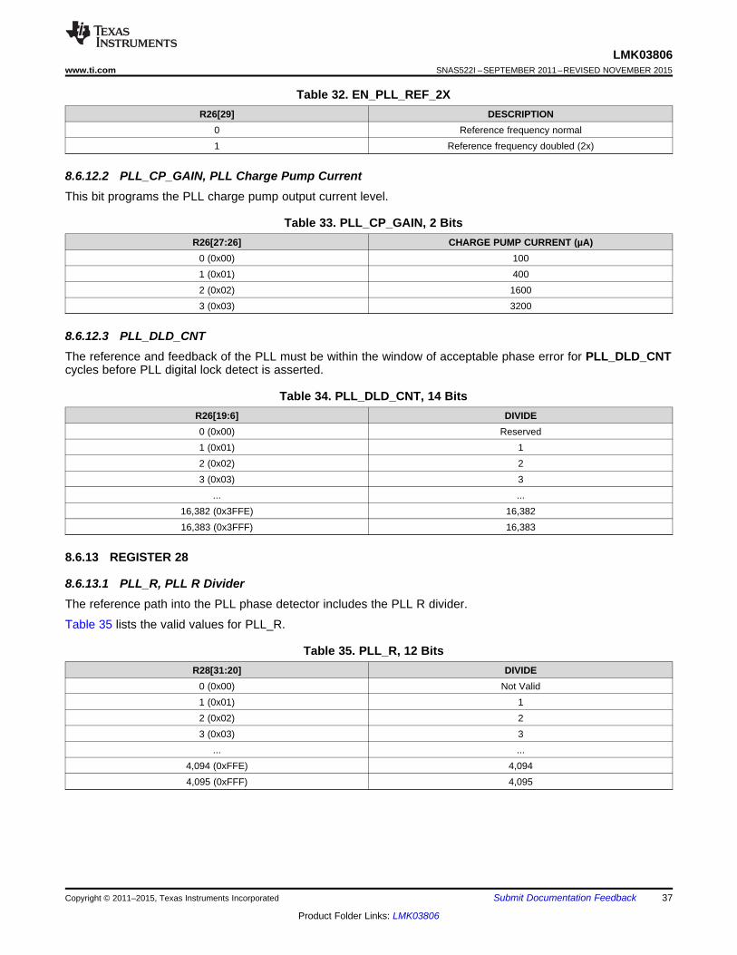
LMK03806www.ti.com SNAS522I –SEPTEMBER 2011–REVISED NOVEMBER 2015
Table 32. EN_PLL_REF_2XR26[29] DESCRIPTION
0 Reference frequency normal1 Reference frequency doubled (2x)
8.6.12.2 PLL_CP_GAIN, PLL Charge Pump CurrentThis bit programs the PLL charge pump output current level.
Table 33. PLL_CP_GAIN, 2 BitsR26[27:26] CHARGE PUMP CURRENT (µA)
0 (0x00) 1001 (0x01) 4002 (0x02) 16003 (0x03) 3200
8.6.12.3 PLL_DLD_CNTThe reference and feedback of the PLL must be within the window of acceptable phase error for PLL_DLD_CNTcycles before PLL digital lock detect is asserted.
Table 34. PLL_DLD_CNT, 14 BitsR26[19:6] DIVIDE0 (0x00) Reserved1 (0x01) 12 (0x02) 23 (0x03) 3
... ...16,382 (0x3FFE) 16,38216,383 (0x3FFF) 16,383
8.6.13 REGISTER 28
8.6.13.1 PLL_R, PLL R DividerThe reference path into the PLL phase detector includes the PLL R divider.
Table 35 lists the valid values for PLL_R.
Table 35. PLL_R, 12 BitsR28[31:20] DIVIDE
0 (0x00) Not Valid1 (0x01) 12 (0x02) 23 (0x03) 3
... ...4,094 (0xFFE) 4,0944,095 (0xFFF) 4,095
Copyright © 2011–2015, Texas Instruments Incorporated Submit Documentation Feedback 37
Product Folder Links: LMK03806

LMK03806SNAS522I –SEPTEMBER 2011–REVISED NOVEMBER 2015 www.ti.com
8.6.14 REGISTER 29
8.6.14.1 OSCin_FREQ, PLL Oscillator Input Frequency RegisterThe frequency of the PLL reference input to the PLL Phase Detector (OSCin/OSCin* port) must be programmedin order to support proper operation of the frequency calibration routine which locks the internal VCO to thetarget frequency.
Table 36. OSCin_FREQ, 3 BitsR29[26:24] OSCin FREQUENCY
0 (0x00) 0 to 63 MHz1 (0x01) >63 MHz to 127 MHz2 (0x02) >127 MHz to 255 MHz3 (0x03) Reserved4 (0x04) >255 MHz to 500 MHz
8.6.14.2 PLL_N_CAL, PLL N Calibration DividerDuring the frequency calibration routine, the PLL uses the divide value of the PLL_N_CAL register instead of thedivide value of the PLL_N register to lock the VCO to the target frequency.
Table 37. PLL_N_CAL, 18 BitsR29[22:5] DIVIDE0 (0x00) Not Valid1 (0x01) 12 (0x02) 2
... ...262,143 (0x3FFFF) 262,143
8.6.15 REGISTER 30Programming Register 30 triggers the frequency calibration routine. This calibration routine will also generate aSYNC event.
8.6.15.1 PLL_P, PLL N Prescaler DividerThe PLL N Prescaler divides the output of the VCO and is connected to the PLL N divider.
Table 38. PLL_P, 3 BitsR30[26:24] DIVIDE VALUE
0 (0x00) 81 (0x01) 22 (0x02) 23 (0x03) 34 (0x04) 45 (0x05) 56 (0x06) 67 (0x07) 7
8.6.15.2 PLL_N, PLL N DividerThe feeback path into the PLL phase detector includes the PLL N divider.
Each time register 30 is updated through the MICROWIRE interface, a frequency calibration routine runs to lockthe VCO to the target frequency. During this calibration PLL_N is substituted with PLL_N_CAL.
38 Submit Documentation Feedback Copyright © 2011–2015, Texas Instruments Incorporated
Product Folder Links: LMK03806

LMK03806www.ti.com SNAS522I –SEPTEMBER 2011–REVISED NOVEMBER 2015
Table 39 lists the valid values for PLL_N.
Table 39. PLL_N, 18 BitsR30[22:5] DIVIDE0 (0x00) Not Valid1 (0x01) 12 (0x02) 2
...262,143 (0x3FFFF) 262,143
8.6.16 REGISTER 31
8.6.16.1 READBACK_ADDR
Table 40. READBACK_ADDRR31[20:16] STATE
0 R01 R12 R23 R34 R45 R56 R67 R78 R89 R910 R1011 R1112 R1213 R1314 R1415 Reserved16 R1617 Reserved... ...23 Reserved24 R2425 Reserved26 R2627 Reserved28 R2829 R2930 R30
Copyright © 2011–2015, Texas Instruments Incorporated Submit Documentation Feedback 39
Product Folder Links: LMK03806

LMK
0380
6OSCin
OSCout
C1
C2
XTALRLIM
LMK03806SNAS522I –SEPTEMBER 2011–REVISED NOVEMBER 2015 www.ti.com
8.6.16.2 uWire_LOCKSetting uWire_LOCK will prevent any changes to uWire registers R0 to R30. Only by clearing the uWire_LOCKbit in R31 can the uWire registers be unlocked and written to once more.
It is not necessary to lock the registers to perform a readback operation.
Table 41. uWire_LOCKR31[5] STATE
0 Registers unlocked1 Registers locked, Write-protect
9 Application and Implementation
NOTEInformation in the following applications sections is not part of the TI componentspecification, and TI does not warrant its accuracy or completeness. TI’s customers areresponsible for determining suitability of components for their purposes. Customers shouldvalidate and test their design implementation to confirm system functionality.
9.1 Application Information
9.1.1 Crystal InterfaceThe LMK03806 has an integrated crystal oscillator circuit on that supports a fundamental mode, AT-cut crystal.The crystal interface is shown in Figure 13.
Figure 13. Crystal Interface
The load capacitance (CL) is specific to the crystal, but usually on the order of 18 - 20 pF. While CL is specifiedfor the crystal, the OSCin input capacitance (CIN = 6 pF typical) of the device and PCB stray capacitance (CSTRAY~ 1~3 pF) can affect the discrete load capacitor values, C1 and C2.
For the parallel resonant circuit, the discrete capacitor values can be calculated as follows:CL = (C1 × C2) / (C1 + C2) + CIN + CSTRAY (1)
Typically, C1 = C2 for optimum symmetry, so Equation 1 can be rewritten in terms of C1 only:CL = C1
2 / (2 × C1) + CIN + CSTRAY (2)
Finally, solve for C1:C1 = (CL – CIN – CSTRAY) × 2 (3)
Electrical Characteristics provides crystal interface specifications with conditions that ensure start-up of thecrystal, but it does not specify crystal power dissipation. The designer will need to ensure the crystal powerdissipation does not exceed the maximum drive level specified by the crystal manufacturer. Overdriving thecrystal can cause premature aging, frequency shift, and eventual failure. Drive level should be held at a sufficientlevel necessary to start-up and maintain steady-state operation.
The power dissipated in the crystal, PXTAL, can be computed by:
40 Submit Documentation Feedback Copyright © 2011–2015, Texas Instruments Incorporated
Product Folder Links: LMK03806

LMK
0380
6
OSCin
OSCin*0.1 PF
51C1
OSC
C2
LMK
0380
6
OSCin
OSCin*
0.1 PF
51C1
OSC
C2
33
LMK03806www.ti.com SNAS522I –SEPTEMBER 2011–REVISED NOVEMBER 2015
Application Information (continued)PXTAL = IRMS
2 × RESR × (1 + C0/CL)2
where• IRMS is the RMS current through the crystal.• RESR is the maximum equivalent series resistance specified for the crystal• CL is the load capacitance specified for the crystal• C0 is the minimum shunt capacitance specified for the crystal (4)
IRMS can be measured using a current probe (for example, Tektronix CT-6 or equivalent) placed on the leg of thecrystal connected to OSCin* with the oscillation circuit active.
As shown in Figure 13, an external resistor, RLIM, can be used to limit the crystal drive level, if necessary. If thepower dissipated in the selected crystal is higher than the drive level specified for the crystal with RLIM shorted,then a larger resistor value is mandatory to avoid overdriving the crystal. However, if the power dissipated in thecrystal is less than the drive level with RLIM shorted, then a zero value for RLIM can be used. As a starting point, asuggested value for RLIM is 1.5 kΩ.
9.1.2 Driving OSCin Pins With a Single-Ended SourceThe LMK03806 has an the ability to be driven by an external reference. Typical external reference interfaces areshown in Figure 14 and Figure 15.
In applications where the external reference amplitude is less than the VOSCin specification of 2.4 Vpp Figure 14 isan appropriate method of interfacing the reference to the LMK03806.
In applications where the external reference amplitude is greater than the VOSCin specification of 2.4 VppFigure 15 is an appropriate method of interfacing the reference to the LMK03806.
In both cases C1 and C2 should be present a low impedance at the reference frequency. A typical value for C1and C2 is 0.1 µF.
Figure 14. LVCMOS External Reference Interface Figure 15. 3.3 Vpp External Reference Interface
Using an external reference, such as a crystal oscillator (XO), may provide better phase noise than a crystal atoffsets below the loop bandwidth. If the jitter integration bandwidth for the application of interest is above the loopfilter bandwidth, the added phase noise of a crystal will not be a significant jitter contributor and may be a morecost effective solution than an XO. Also, operating at higher reference frequencies allows higher phase detectorfrequencies, which also improves in band PLL phase noise performance.
9.1.3 Driving OSCin Pins With a Differential SourceThe OSCin port can be driven by differential signals. The LMK03806 internally biases the input pins so thedifferential interface should be AC coupled. The recommended circuits for driving the OSCin pins with eitherLVDS or LVPECL are shown below.
Copyright © 2011–2015, Texas Instruments Incorporated Submit Documentation Feedback 41
Product Folder Links: LMK03806

0.1 µF
0.1 µF100 100- Trace
(Differential)
OSCin
OSCin*
LVPECL
240
240
0.1 µF
0.1 µF
LMK
0380
6
0.1 µF
0.1 µF100 100- Trace
(Differential)
OSCin
OSCin*
LVDS
LMK
0380
6
LMK03806SNAS522I –SEPTEMBER 2011–REVISED NOVEMBER 2015 www.ti.com
Application Information (continued)
Figure 16. OSCin/OSCin* Termination for an LVDS Reference Clock Source
Figure 17. OSCin/OSCin* Termination for an LVPECL Reference Clock Source
9.1.4 Frequency Planning With the LMK03806Calculating the value of the output dividers is simple due to the architecture of the LMK03806. That is, the clockoutput dividers allow for even and odd output divide values from 2 to 1045. The procedure for determining thePLL and clock output divider values for a set of clock output frequencies is straightforward.1. Calculate the least common multiple (LCM) of the clock output frequencies.2. Determine which VCO frequency will support the target clock output frequencies given the LCM.3. Determine the clock output divide values based on VCO frequency.4. Determine the PLL divider values – VCO_DIV, PLL_P, PLL_N, and PLL_R – to allow the VCO frequency to
lock to the OSCin frequency. For best in-band PLL noise, try to maximize the PLL phase detector frequencyby using the smallest PLL divider values and enabling the PLL doubler.
For example, given the following target output frequencies: 156.25 MHz, 125 MHz, 100 MHz, and 25 MHz with aOSCin frequency of 20 MHz:1. Determine the LCM of the three frequencies. LCM(156.25, 125, 100, 25) = 2500 MHz. The LCM frequency is
the lowest frequency for which all of the target output frequencies are integer divisors of the LCM. Note: ifthere is one frequency which causes the LCM to be very large, greater than 2.6 GHz for example, determineif there is a single frequency requirement which causes this. It may be possible to select the crystalfrequency to satisfy this frequency requirement through OSCout or CLKout6/7/8/9 driven by OSCin. In thisway it is possible to get non-integer related frequencies at the outputs.
2. Multiply the LCM frequency by an integer value that causes the product (LCM * x) to fall into the valid VCOfrequency range from 2370 to 2600 MHz. In this case, the LCM frequency of 2500 MHz is already within theVCO frequency.
3. Continuing the example by using a VCO frequency of 2500 MHz, the CLKout dividers can be calculated bysimply dividing the VCO frequency by the output frequency. To output 156.25 MHz, 125 MHz, 100 MHz, and25 MHz, the output dividers will be 16, 20, 25, and 100, respectively.(a) 2500 MHz / 156.25 MHz = 16(b) 2500 MHz / 125 MHz = 20(c) 2500 MHz / 100 MHz = 25(d) 2500 MHz / 25 MHz = 100
4. The PLL must be locked to its input reference. Refer to Configuring the PLL for more information on thistopic. By programming the clock output dividers and the PLL dividers, the VCO can be locked to 2500 MHz
42 Submit Documentation Feedback Copyright © 2011–2015, Texas Instruments Incorporated
Product Folder Links: LMK03806

LMK03806www.ti.com SNAS522I –SEPTEMBER 2011–REVISED NOVEMBER 2015
Application Information (continued)and the clock outputs dividers can each divide-down the VCO frequency to the achieve the target outputfrequencies.
Refer to Application Note AN-1865, Frequency Synthesis and Planning for PLL Architectures (SNAA061) formore information on this topic and LCM calculations.
9.1.5 Configuring the PLLFor the PLL to operate in closed-loop mode, the following relationships in Equations 5 and 6 must be satisfied toensure the PLL phase detector input frequencies for the reference and feedback paths are equal.
Fpd = Fosc * PLL_D / PLL_R (PLL reference path) (5)Fpd = Fvco / (PLL_P * PLL_N) (PLL feedback path)
where• Fpd = PLL phase detector frequency (Fpd ≤ 155 MHz)• FOSCin = OSCin reference frequency (Fosc ≤ 500 MHz)• Fvco = VCO frequency (VCO tuning range = 2370 to 2600 MHz)• PLL_D = PLL reference doubler mode (Disabled = 1, Enabled = 2)• PLL_R = PLL reference divider (values = 1 to 4095)• PLL_P = PLL N prescaler divider (values = 2 to 8)• PLL_N = PLL N divider (values = 1 to 262143) (6)
NOTEWhen FOSCin and Fpd are equal, the best PLL in-band noise can be achieved with the PLLreference doubler enabled (EN_PLL_REF_2X=1) and the PLL reference divider is 2(PLL_R =2), rather than with the doubler disabled (EN_PLL_REF_2X=0) and PLLreference divider of 1 (PLL_R=1).
The output frequency is related to Fvco as follows.FCLKout = Fvco / OUT_DIV
where• OUT_DIV: Output channel divider (value = 1 to 1045) (7)
9.1.5.1 Example PLL ConfigurationContinuing the example above, we are given the target output frequencies of 156.25 MHz, 125 MHz, 100 MHz,and 25 MHz with an OSCin frequency of 20 MHz. As previously calculated, the LCM and Fvco is 2500 MHz.
First, we will consider the PLL reference path. For lowest possible in-band PLL flat noise, we will try to maximizephase detector frequency. In this case, the highest Fpd possible from the reference path is 40 MHz (with thereference doubler enabled, doubling the 20 MHz OSCin). However, since 40 MHz does not divide into 2500 MHzby an integer value (and thus is unable to be reproduced by the PLL feedback path), we are required to use anFpd of 20 MHz instead, which does divide into 2500 by an integer value of 125. As noted above, when FOSCin andFpd are equal, the best PLL in-band noise can be achieved with the PLL reference doubler enabled(EN_PLL_REF_2X=1) and the PLL reference divider is 2 (PLL_R =2).
Next, we will consider the PLL feedback path. As determined earlier, Fvco is 2500 MHz and Fpd is 20 MHz, whichis 2500 MHz divided by 125. The prescaler and N divider settings together must divide Fvco by 125. Given thatthe prescaler can be set between 2 to 8 and the N divider can be set between 1 to 262,143, the only setting thatwould work in this case is a prescaler value of 5 and an N divider value of 25. Note that in a case where multipleconfigurations are possible, increasing the N divider value will reduce loop filter component sizes.
Copyright © 2011–2015, Texas Instruments Incorporated Submit Documentation Feedback 43
Product Folder Links: LMK03806

2e6 × 3.7 ns × fPD
PLL_DLD_CNTppm =
NO
NO
YES
YES
YES
Phase Error < â
Lock Detected = FalseLock Count = 0
Lock Count =DLD_CNT
Phase Error > âNO YES
START
IncrementLock Count
Lock Detected = True
LMK03806SNAS522I –SEPTEMBER 2011–REVISED NOVEMBER 2015 www.ti.com
Application Information (continued)9.1.6 Digital Lock DetectThe digital lock detect circuit is used to determine the lock status of the PLL. The flowchart in Figure 18 showsthe general way this circuit works.
EVENT PLL WINDOW SIZE (ε) LOCK COUNTPLL Locked PLL 3.7 ns PLL_DLD_CNT
For a digital lock detect event to occur there must be a number of PLL phase detector cycles during which thetime/phase error of the PLL_R reference and PLL_N feedback signal edges are within the 3.7 ns window size ofthe LMK03806. Lock count is the term which is used to specify how many PLL phase detector cycles have beenwithin the window size of 3.7 ns at any given time. Since there must be a specified number phase detectorevents before a lock event occurs, a minimum digital lock event time can be calculated as lock count / Fpd.
Figure 18. Digital Lock Detect Flow Diagram
A user specified ppm accuracy for lock detect is programmable using a lock count register. By using Equation 8,values for a lock count and window size can be chosen to set the frequency accuracy required by the system inppm before the digital lock detect event occurs. Units of Fpd are Hertz:
(8)
The effect of the lock count value is that it shortens the effective lock window size by dividing the window size bylock count.
44 Submit Documentation Feedback Copyright © 2011–2015, Texas Instruments Incorporated
Product Folder Links: LMK03806

LMK03806www.ti.com SNAS522I –SEPTEMBER 2011–REVISED NOVEMBER 2015
If at any time the PLL_R reference and PLL_N feedback signals are outside the time window set by window size,then the lock count value is reset to 0.
For example, we will calculate the minimum PLL digital lock time given a PLL Fpd of 40 MHz and PLL_DLD_CNT= 10,000. The minimum lock time of PLL will be 10,000 / 40 MHz = 250 µs.
Copyright © 2011–2015, Texas Instruments Incorporated Submit Documentation Feedback 45
Product Folder Links: LMK03806

R
N
Phase Detector/ChargePump
InternalVCO
OSCin
OSCoutXOSCoutX*
LMK03806
CPout
Divider
CLKoutYCLKoutY*
CLKoutXCLKoutX*
Partially
Integrated Loop Filter
12 outputs
External Loop Filter
PLL 6 blocks
2 outputs
OSCin*
Div
LMK03806SNAS522I –SEPTEMBER 2011–REVISED NOVEMBER 2015 www.ti.com
9.2 Typical ApplicationNormal use case of the LMK03806 device is as a clock generator. This section will discuss a design example toshow the various functional aspects of the LMK03806 device.
Figure 19. Simplified Functional Block Diagram
9.2.1 Design RequirementsA networking line card type application needs a clocking solution for an ASIC, FPGA, CPU, PCIe 3.0 interface,and a 10G PHY. The input clock will be a crystal oscillator. A summary of clock input and output requirementsare as follows:
Clock Input:• 20 MHz oscillator
Clock Outputs:• 2x 156.25-MHz LVPECL clock for ASIC• 2x 156.25-MHz LVPECL clock for 10G PHY• 4x 100-MHz HCSL for PCIe 3.0• 2x 100-MHz LVDS for FPGA• 2x 50-MHz LVCMOS for CPU
The following information reviews the steps to produce this design.
9.2.2 Detailed Design ProcedureDesign of all aspects of the LMK03806 is quite involved and software has been written to assist in part selection,part programming, loop filter design, and simulation. This design procedure will give a quick outline of theprocess.
NOTEThis information is current as of the date of the release of this datasheet. Design toolsreceive continuous enhancements to add features and improve model accuracy. Refer tosoftware instructions or training for latest features.
1. Device Selection– The key to device selection is the required Fvco given the required output frequencies. The device must be
able to produce a Fvco that can be divided down to required output frequencies.– The software design tools will take into account the Fvco range for specific devices based on the
application's required output frequencies.2. Device Configuration
– There are many possible permutations of dividers and other registers to get same output frequenciesfrom a device. However there are some optimizations and trade-offs to be considered.– If more than one divider is in series, for instance PLL prescaler followed by PLL N divider, it is
possible although not assured that some crosstalk/mixing could be created when using some divides.– The design software normally attempts to maximize Fpd, use smallest dividers, and maximize PLL charge
46 Submit Documentation Feedback Copyright © 2011–2015, Texas Instruments Incorporated
Product Folder Links: LMK03806

LMK03806www.ti.com SNAS522I –SEPTEMBER 2011–REVISED NOVEMBER 2015
Typical Application (continued)pump current.
– Refer to Configuring the PLL for divider equations to ensure the PLL is locked. The design software isable to configure the device for most cases.
– These guidelines may be followed when configuring PLL related dividers or other related registers:– For lowest possible in-band PLL flat noise, maximize Fpd to minimize N divide value.– For lowest possible in-band PLL flat noise, maximize charge pump current. Higher value charge pump
currents often yield similar performance.– To reduce loop filter component sizes, increase the total feedback divide value (PLL_P * PLL_N)
and/or reduce charge pump current.– As rule of thumb, keep Fpd approximately between 10 * PLL loop bandwidth and 100 * PLL loop
bandwidth. An Fpd value less than 5 * PLL bandwidth may be unstable and a Fpd > 100 * loopbandwidth may experience increased lock time due to cycle slipping.
3. PLL Loop Filter Design– TI recommends to use Clock Design Tool or Clock Architect to design your loop filter.– The Clock Design Tool will return solutions with high reference/phase detector frequencies by default. In
the Clock Design Tool the user may choose to increase the reference divider to reduce the Fpd to achievea narrow loop bandwidth, so it is possible to reduce loop filter capacitor to a practical value.
– While designing the loop filter, adjusting the charge pump current and/or the total feedback divide value(PLL_P * PLL_N) can help with loop filter component selection. Lower charge pump currents and larger Nvalues result in smaller loop filter capacitor values but at the expense of increased in-band PLL phasenoise.
– More detailed understanding of PLL loop filter design can found in PLL Performance, Simulation, andDesign (www.ti.com/tool/pll_book).
4. Clock Output Assignment– At this point of time, the design software does not take into account frequency assignment to specific
outputs except to ensure that the output frequencies can be achieved. It is best to consider proximity ofeach clock output to each other and other PLL circuitry when choosing final clock output locations. Hereare some guidelines to help achieve best performance when assigning outputs to specificCLKout/OSCout pins.– Group common frequencies together.– PLL charge pump circuitry can cause crosstalk at charge pump frequency. Place outputs sharing
charge pump frequency or lower priority outputs that are not sensitive to charge pump frequencyspurs together.
5. Other device specific configuration. For LMK03806 consider the following:– PLL digital lock detect based on programming:
– There is a digital lock detect circuit which is used to determine the lock status of the PLL. It can alsobe used to ensure a specific frequency accuracy. A user specified frequency accuracy required totrigger a lock detect event is programmable using a lock count register. Refer to Digital Lock Detectfor more information.
6. Device Programming– The software tool CodeLoader for EVM programming can be used to set up the device in the desired
configuration, then export a hex register map suitable for use in application. Some additional informationon each part of the design procedure for the example is outlined below.
Copyright © 2011–2015, Texas Instruments Incorporated Submit Documentation Feedback 47
Product Folder Links: LMK03806

LMK03806SNAS522I –SEPTEMBER 2011–REVISED NOVEMBER 2015 www.ti.com
Typical Application (continued)9.2.2.1 Device SelectionWEBENCH Clock Architect Tool or Clock Design Tool can be used as aids in device selection. Enter therequired frequencies and formats into the tools. To find this device, select a solution based on LMK03806B(referring to the evaluation board).
9.2.2.1.1 Clock Architect
When generating solutions, it is possible to narrow the parts used in the solution by setting the appropriate partfilter.
9.2.2.1.2 Clock Design Tool
In wizard-mode, select Single PLL and fill in the input frequency and desired output frequencies to generate a listof solutions. If the example values are used, the LMK03806 should be listed as the first result.
9.2.2.1.3 Calculation Using LCM
In this example, the LCM of 156.25 MHz, 100 MHz, and 50 MHz = 2500 MHz. This value is a valid Fvco for theLMK03806. Therefore, it may be used to produce these output frequencies.
9.2.2.2 Device ConfigurationThe tools listed above automatically configure the clock solution to meet the input and output frequencyrequirements given and make assumptions about certain parameters to give default simulation results. Theassumptions made are to maximize input frequencies, Fpd, and charge pump currents while minimizing Fvco anddivider values. We will also outline the steps for manually configuring the device below for greater flexibility. Notethat this procedure is the same as the one outlined in the Frequency Planning With the LMK03806 andConfiguring the PLL sections, which can be referenced for a more detailed explanation.
We are given the target output frequencies of 156.25 MHz, 125 MHz, 100 MHz, and 25 MHz with an FOSCin of 20MHz. As previously calculated, the LCM and Fvco is 2500 MHz.
First, we will consider the PLL reference path. For lowest possible in-band PLL flat noise, we will try to maximizeFpd. 20 MHz is the highest frequency which divides into 2500 MHz by an integer value and which can also besynthesized from FOSCin. As noted earlier, when FOSCin and fpd are equal, the best PLL in-band noise can beachieved with the PLL reference doubler enabled (EN_PLL_REF_2X=1) and the PLL reference divider is 2(PLL_R =2).
Next, we will consider the PLL feedback path. As determined earlier, Fvco is 2500 MHz and the Fpd is 20 MHz,which is 2500 MHz divided by 125. The prescaler and N divider settings together must divide Fvco by 125. Theonly setting that works in this case is a prescaler value of 5 and an N divider value of 25.
At this point the design meets all input and output frequency requirements and it is possible to design a loop filterfor the application and simulate phase noise of the output clocks.
9.2.2.3 PLL Loop Filter DesignAt this time, the user may choose to use the simulation tools for more accurate simulations. For example:• Clock Design Tool allows loading a custom phase noise profile for various blocks. Typically, a custom phase
noise plot is entered for OSCin to match the reference phase noise to the device. For improved accuracy insimulation and optimum loop filter design, be sure to load these custom noise profiles for use in application.After loading a phase noise plot, user should recalculate the recommended loop filter design.
• The Clock Design Tool will return solutions with high reference/phase detector frequencies by default. In theClock Design Tool the user may increase the reference divider to reduce the frequency if desired. Forexample, if a narrow loop bandwidth is desired, it is possible to reduce Fpd by increasing the PLL R divider.
Note: Clock Design Tool provides some recommended loop filters upon first loading the simulation. These valuesare not re-calculated any time PLL related values are changed (for example, input phase noise, charge pumpcurrent, divider values, etc.), so it is recommended to re-design the PLL loop filter, either by manually enteringdesired values, or by using the ‘Design a Loop Filter’ button in the LOOPFILTER box.
48 Submit Documentation Feedback Copyright © 2011–2015, Texas Instruments Incorporated
Product Folder Links: LMK03806

LMK03806www.ti.com SNAS522I –SEPTEMBER 2011–REVISED NOVEMBER 2015
Typical Application (continued)9.2.2.3.1 Example Loop Filter Design
In the LOOPFILTER box, there are options for displaying a bode plot, simulating phase noise, and re-calculatingloop filter values. Selecting the ‘Design a Loop Filter’ button brings up a window where a target bandwidth andphase margin can be entered and the tool will re-design the loop filter component values to converge to thespecified targets. Component values can also be manually entered and the tool will calculate the resulting loopfilter parameters.
For this example, a custom phase noise plot was uploaded based on measured data for the reference oscillatorinput. Fpd was set to 20 MHz and loop filter was optimized to achieve a loop bandwidth of 62 kHz and phasemargin of 76°. The loop filter values used were C1 = 220 pF, C2 = 18 nF, R2 = 820 Ω, C3 = 10 pF, R3 = 200 Ω,C4 = 10 pF, and R4 = 200 Ω. The charge pump current was set to 3.2 mA.
9.2.2.4 Other Device Specific Configuration
9.2.2.4.1 Digital Lock Detect
Digital lock time for the PLL will ultimately depend upon the programming of the PLL_DLD_CNT register asdiscussed in Digital Lock Detect. Since the PLL Fpd in this example is 20 MHz, the lock time will =PLL_DLD_CNT / 20 MHz. If PLL_DLD_CNT is set to 10,000, the lock time will be 0.5 ms. The ppm accuracyrequired to indicate lock will be (2e6 * 3.7 ns * fpd) / PLL_DLD_CNT, or 14.8 ppm. Refer to Digital Lock Detect formore detail on calculating lock times.
9.2.2.5 Device ProgrammingThe CodeLoader software is used to program the LMK03806B evaluation board using the LMK03806B profile. Italso allows the exporting of a register map which can be used to program the device to the user’s desiredconfiguration. Once a configuration of dividers has been achieved using the Clock Design Tool to meet therequested input/output frequencies with the desired performance, the CodeLoader software needs to bemanually updated with this configuration to meet the required application. At this time no automatic importbetween the two tools exists.
Copyright © 2011–2015, Texas Instruments Incorporated Submit Documentation Feedback 49
Product Folder Links: LMK03806

LMK03806SNAS522I –SEPTEMBER 2011–REVISED NOVEMBER 2015 www.ti.com
Typical Application (continued)9.2.3 Application CurvesThe following jitter and phase noise data was captured from an LMK03806 evaluation board. Fvco was set to2500 MHz and Fpd was set to 20 MHz. In order to obtain a loop bandwidth of 62 kHz and a phase margin of 76°,the loop filter values used were C1 = 220 pF, C2 = 18 nF, R2 = 820 Ω, C3 = 10 pF, R3 = 200 Ω, C4 = 10 pF,and R4 = 200 Ω. The charge pump current was set to 3.2 mA.
Figure 21. LVDS Phase Noise, 100 MHzFigure 20. LVPECL Phase Noise, 156.25 MHz
Figure 22. LVCMOS Phase Noise, 50 MHz
50 Submit Documentation Feedback Copyright © 2011–2015, Texas Instruments Incorporated
Product Folder Links: LMK03806

LMK03806www.ti.com SNAS522I –SEPTEMBER 2011–REVISED NOVEMBER 2015
Typical Application (continued)The following PCIe 3.0 phase jitter results were obtained using the Intel Clock Jitter Tool using waveform datacaptured with an Agilent DSA90804A. The RMS jitter result of 0.107 ps easily meets the PCIe 3.0 jitterrequirement of 1ps with significant margin.
Figure 24. PCIe 3.0 RMS Jitter, 100-MHz HCSLFigure 23. PCIe 3.0 Phase Jitter, 100-MHz HCSL
Copyright © 2011–2015, Texas Instruments Incorporated Submit Documentation Feedback 51
Product Folder Links: LMK03806

LEuWire
CLKuWire
DATAuWire
To Hostprocessor
LDObyp1
LDObyp2
10 PF 0.1 PF
LMK03806
OSCin
OSCin*
CPout
LoopFilter
CLKout[2:3]*
CLKout[2:3]
0.1 PF
240 Ö
2x 156.25 MHz LVPECL to 10G PHY
0.1 PF
240 Ö
4x 100 MHz HCSL to PCIe 3.0
CLKout11*
CLKout112x 50 MHz LVCMOS 3.3 Vto CPU (complementary phases)
CLKout[0:1]*
CLKout[0:1]
0.1 PF
240 Ö
2x 156.25 MHz LVPECL to ASIC
0.1 PF
240 Ö
CLKout[8:9]*
CLKout[8:9]2x 100 MHz LVDS to FPGA (with 100 Ö on-chip termination)
CLKout[4:7]*
CLKout[4:7]
Clock outputs drive 50-Ö traces (single-ended Zo), and differential clocks are terminated at the receiver inputs.
Unused output pairs (not shown) are left floating and disabled via register control
Readback
Ftest / LD
SYNC
0.1 PF
240 Ö
0.1 PF
240 Ö
56 Ö
56 Ö
470 Ö
470 Ö
3.3V
3.3V
LVPECL-to-HCSL AC-coupled termination
(at receiver inputs)
220 pF(C1)
22 nF(C2)
820 Ö(R2)
1.5 kÖ(RLIM)
22 pF(CL1)
22 pF(CL2)
20-MHz XTALCL = 18 pF
CNR
33 Ö
PLL Supply Plane
10 µF, 1 µF, 0.1 µF
1 µF, 0.1 µF, 10 nF
FBOutput Supply Plane
10 µF, 1 µF, 0.1 µF
FB
Vcc8FB
0.1 µF 0.1 µF
LDOLP3878-ADJ
Vcc[1,4,5,6,7,9] Vcc[13,2]FB
0.1 µF
Vcc[3,10,11,12]FB
0.1 µF
3.3 V
VCO LDO, Digital, OSC, PLL Core
ChargePump
CLKout[0/1,2/3]
CLKout[4/5,6/7,
8/9,10/11]
Vcc Groups
CMOS I/2¶V
PLL Ref. In
LDO Bypass Caps
Clock Outputs
NOTE: DO NOT directly copy schematic for CLKout Vcc[2,3,10,11,12]. This is for an example frequency plan only.
It is recommended to group CLKout Vcc supplies by same frequency and share a ferrite bead for CLKout Vcc at the same
or related frequencies.
FB = Ferrite bead
156.25 MHz Vcc group
100 & 50 MHz Vcc group
LMK03806SNAS522I –SEPTEMBER 2011–REVISED NOVEMBER 2015 www.ti.com
9.3 System Examples
9.3.1 System Level DiagramFigure 25 shows a detailed system level diagram of the example above to serve as a guideline for good practiceswhen designing with the LMK03806.
Figure 25. Example Network Line Card Application
52 Submit Documentation Feedback Copyright © 2011–2015, Texas Instruments Incorporated
Product Folder Links: LMK03806

LMK03806www.ti.com SNAS522I –SEPTEMBER 2011–REVISED NOVEMBER 2015
9.4 Do's and Don'ts
9.4.1 LVCMOS Complementary vs. Non-Complementary Operation• TI recommends to use a complementary LVCMOS output format such as LVCMOS (Norm/Inv) to reduce
switching noise and crosstalk when using LVCMOS.• If only a single LVCMOS output is required, the complementary LVCMOS output format can still be used by
leaving the unused LVCMOS output floating.• A non-complimentary format such as LVCMOS (Norm/Norm) is not recommended as increased switching
noise is present.
9.4.2 LVPECL OutputsWhen using an LVPECL output it is not recommended to place a capacitor to ground on the output as might bedone when using a capacitor input LC lowpass filter. The capacitor will appear as a short to the LVPECL outputdrivers which are able to supply large amounts of switching current. The effect of the LVPECL sourcing largeswitching currents can result in the following:1. Large switching currents through the Vcc pin of the LVPECL power supply resulting in more Vcc noise and
possible Vcc spikes.2. Large switching currents injected into the ground plane through the capacitor which could couple onto other
Vcc pins with bypass capacitors to ground resulting in more Vcc noise and possible Vcc spikes.
9.4.3 Sharing MICROWIRE (SPI) LinesWhen CLKuWire and DATAuWire toggle and an internal VCO mode is used, there may some spurious contenton the phase noise plot related to the frequency of the CLKuWire and DATAuWire pins.
9.4.4 SYNC PinIf the SYNC pin is connected to a host device (for example, FPGA, CPLD, CPU) with noisy I/O power rails, usesmall series resistor and shunt capacitor (CNR) as shown in Figure 25. An external low-pass filter can preventnoise on the SYNC input from coupling unwanted spurious content to nearby internal analog circuitry.
10 Power Supply Recommendations
10.1 Current Consumption and Power Dissipation CalculationsFrom Table 42 the current consumption can be calculated for any configuration.
For example, the current for the entire device with 1 LVDS (CLKout0) and 1 LVPECL 1.6 Vpp with 240-Ω emitterresistors (CLKout1) output active with a clock output divide = 1, and no other features enabled can be calculatedby adding up the following blocks: core current, base clock distribution, clock output group, clock divider, oneLVDS output buffer current, and one LVPECL output buffer current. There will also be one LVPECL outputdrawing emitter current, which means some of the power from the current draw of the device is dissipated in theexternal emitter resistors which doesn't add to the thermal power dissipation budget for the device. In addition toemitter resistor power, power dissipated in the load for LVDS/LVPECL do not contribute to the thermal powerdissipation budget for the device.
For total current consumption of the device, add up the significant functional blocks. In this example, 212.9 mA =• 122 mA (core current)• 17.3 mA (base clock distribution)• 2.8 mA (CLKout group for 2 outputs)• 25.5 mA (CLKout0 & 1 divider)• 14.3 mA (LVDS buffer)• 31 mA (LVPECL 1.6 Vpp buffer /w 240-Ω emitter resistors)
Copyright © 2011–2015, Texas Instruments Incorporated Submit Documentation Feedback 53
Product Folder Links: LMK03806

LMK03806SNAS522I –SEPTEMBER 2011–REVISED NOVEMBER 2015 www.ti.com
Current Consumption and Power Dissipation Calculations (continued)Once total current consumption has been calculated, power dissipated by the device can be calculated. Thepower dissipation of the device is equation to the total current entering the device multiplied by the voltage at thedevice minus the power dissipated in any emitter resistors connected to any of the LVPECL outputs or any otherexternal load power dissipation. Continuing the above example which has 212.9 mA total Icc and one output with240-Ω emitter resistors and one LVDS output. Total IC power = 666 mW = 3.3 V * 212.9 mA - 35 mW - 1.5 mW.
Table 42. Typical Current Consumption for Selected Functional Blocks(TA = 25 °C, VCC = 3.3 V)
POWER POWERTYPICAL DISSIPATED DISSIPATEDBLOCK CONDITION ICC IN DEVICE EXTERNALL(mA) (mW) (1) Y (mW) (2)
CORE AND FUNCTIONAL BLOCKSCore Internal VCO Locked 122 403 -Base Clock At least 1 CLKoutX_Y_PD = 0 17.3 57.1 -Distribution
Each CLKout groupCLKout Group 2.8 9.2 -(CLKout0/1 & 10/11, CLKout2/3 & 4/5, CLKout 6/7 & 8/9)Divide < 25 25.5 84.1 -
Clock DividerDivide >= 25 29.6 97.7 -
SYNC Asserted While SYNC is asserted, this extra current is drawn 1.7 5.6 -Crystal Mode Crystal Oscillator Buffer 1.8 5.9 -OSCin Doubler EN_OSCin_2X = 1 2.8 9.2 -
CLOCK OUTPUT BUFFERSLVDS 100-Ω differential termination 14.3 45.7 1.5
LVPECL 2.0 Vpp, AC coupled using 240-Ω emitter resistors 32 70.6 35LVPECL 1.6 Vpp, AC coupled using 240-Ω emitter resistors 31 67.3 35
LVPECL LVPECL 1.6 Vpp, AC coupled using 120-Ω emitter resistors 46 91.8 60(3)
LVPECL 1.2 Vpp, AC coupled using 240-Ω emitter resistors 30 59 40LVPECL 0.7 Vpp, AC coupled using 240-Ω emitter resistors 29 55.7 40
3 MHz 24 79.2 -LVCMOS Pair (CLKoutX_Y_TYPE= 6 to 10) 30 MHz 26.5 87.5 -CL = 5 pF 150 MHz 36.5 120.5 -
LVCMOS3 MHz 15 49.5 -LVCMOS Single (CLKoutX_Y_TYPE
= 11 to 13) 30 MHz 16 52.8 -CL = 5 pF 150 MHz 21.5 71 -
(1) Assuming θJA = 15 °C/W, the total power dissipated on chip must be less than (125 °C – 85 °C) / 16 °C/W = 2.5 W to guarantee ajunction temperature is less than 125 °C.
(2) Worst case power dissipation can be estimated by multiplying typical power dissipation with a factor of 1.15.(3) Power is dissipated externally in LVPECL emitter resistors. The externally dissipated power is calculated as twice the DC voltage level
of one LVPECL clock output pin squared over the emitter resistance. That is to say power dissipated in emitter resistors = 2 * Vem2 /Rem.
11 Layout
11.1 Layout GuidelinesPower consumption of the LMK03806 can be high enough to require attention to thermal management. Forreliability and performance reasons the die temperature should be limited to a maximum of 125°C. That is, as anestimate, TA (ambient temperature) plus device power consumption times θJA should not exceed 125°C.
54 Submit Documentation Feedback Copyright © 2011–2015, Texas Instruments Incorporated
Product Folder Links: LMK03806

0.2 mm
1.46 mm
7.2 mm
1.15 mm
LMK03806www.ti.com SNAS522I –SEPTEMBER 2011–REVISED NOVEMBER 2015
Layout Guidelines (continued)The package of the device has an exposed pad that provides the primary heat removal path as well as excellentelectrical grounding to a printed-circuit-board. To maximize the removal of heat from the package a thermal landpattern including multiple vias to a ground plane must be incorporated on the PCB within the footprint of thepackage. The exposed pad must be soldered down to ensure adequate heat conduction out of the package.
A recommended land and via pattern is shown in Figure 26. More information on soldering WQFN packages andgerber footprints can be obtained: http://www.ti.com/packaging.
A recommended footprint including recommended solder mask and solder paste layers can be found at:http://www.ti.com/packaging for the NKD0064A package.
Figure 26. Recommended Land and Via Pattern
To minimize junction temperature, TI recommends that a simple heat sink be built into the PCB (if the groundplane layer is not exposed). This is done by including a copper area of about 2 square inches on the oppositeside of the PCB from the device. This copper area may be plated or solder coated to prevent corrosion butshould not have conformal coating (if possible), which could provide thermal insulation. The vias shown inFigure 26 should connect these top and bottom copper layers and to the ground layer. These vias act as heatpipes to carry the thermal energy away from the device side of the board to where it can be more effectivelydissipated.
Copyright © 2011–2015, Texas Instruments Incorporated Submit Documentation Feedback 55
Product Folder Links: LMK03806

LMK03806SNAS522I –SEPTEMBER 2011–REVISED NOVEMBER 2015 www.ti.com
11.2 Layout Example
Figure 27. LMK03806 Layout Example
Crystal input to OSCin pins (purple circle):• Place crystal with associated load capacitors (C6 and C9) as close as possible to the chip, and use
short/direct routing to the OSCin pins.• If possible, cut out both ground plane and power plane under the area where the crystal and the routing to the
device are placed. In this area, avoid using vias in the crystal signal path and routing other signals below thecrystal paths, as these could be potential areas for noise coupling.
Clock outputs (blue circles):• Differential signals should be routed tightly coupled to minimize PCB crosstalk. Trace impedance and
loading/terminations should be designed according to output type being used (that is, LVDS, LVPECL...).• Unused output pins should be left open without connection to a trace. Unused outputs should be powered
down through registers to reduce power and switching noise.
Power pins (green rectangles):• Place ferrite beads and bypass caps as close as possible to the Vcc pins as possible. Design a low
impedance power distribution network over a wide frequency range using multiple decoupling and bypasscaps with different values/sizes. Use ferrite beads to isolate the device supply pins from board noise sources.
Loop filter (orange oval):• Place loop filter resistor and capacitors nearby the chip, and route loop filter nodes from digital traces or noisy
power traces/planes to avoid noise coupling.
56 Submit Documentation Feedback Copyright © 2011–2015, Texas Instruments Incorporated
Product Folder Links: LMK03806

LMK03806www.ti.com SNAS522I –SEPTEMBER 2011–REVISED NOVEMBER 2015
12 Device and Documentation Support
12.1 Device Support
12.1.1 Development SupportFor additional support, see the following:• Clock Design Tool: http://www.ti.com/tool/clockdesigntool• Clock Architect: http://www.ti.com/lsds/ti/analog/webench/clock-architect.page• Loop Filter Design: PLL Performance, Simulation, and Design (www.ti.com/tool/pll_book)
12.2 Documentation Support
12.2.1 Related DocumentationFor additional information, see the following:• Common Data Transmission Parameters and their Definitions, Application Note AN-912 (SNLA036)• Crystal Based Oscillator Design with the LMK04000 Family, Application Note AN-1939 (SNAA065)• Frequency Synthesis and Planning for PLL Architectures, Application Note AN-1865 (SNAA061)
12.3 Related LinksThe table below lists quick access links. Categories include technical documents, support and communityresources, tools and software, and quick access to sample or buy.
Table 43. Related LinksTECHNICAL TOOLS & SUPPORT &PARTS PRODUCT FOLDER SAMPLE & BUY DOCUMENTS SOFTWARE COMMUNITY
LMK03806 Click here Click here Click here Click here Click here
12.4 Community ResourceThe following links connect to TI community resources. Linked contents are provided "AS IS" by the respectivecontributors. They do not constitute TI specifications and do not necessarily reflect TI's views; see TI's Terms ofUse.
TI E2E™ Online Community TI's Engineer-to-Engineer (E2E) Community. Created to foster collaborationamong engineers. At e2e.ti.com, you can ask questions, share knowledge, explore ideas and helpsolve problems with fellow engineers.
Design Support TI's Design Support Quickly find helpful E2E forums along with design support tools andcontact information for technical support.
12.5 TrademarksE2E is a trademark of Texas Instruments.All other trademarks are the property of their respective owners.
12.6 Electrostatic Discharge CautionThese devices have limited built-in ESD protection. The leads should be shorted together or the device placed in conductive foamduring storage or handling to prevent electrostatic damage to the MOS gates.
12.7 GlossarySLYZ022 — TI Glossary.
This glossary lists and explains terms, acronyms, and definitions.
Copyright © 2011–2015, Texas Instruments Incorporated Submit Documentation Feedback 57
Product Folder Links: LMK03806

LMK03806SNAS522I –SEPTEMBER 2011–REVISED NOVEMBER 2015 www.ti.com
13 Mechanical, Packaging, and Orderable InformationThe following pages include mechanical, packaging, and orderable information. This information is the mostcurrent data available for the designated devices. This data is subject to change without notice and revision ofthis document. For browser-based versions of this data sheet, refer to the left-hand navigation.
58 Submit Documentation Feedback Copyright © 2011–2015, Texas Instruments Incorporated
Product Folder Links: LMK03806

PACKAGE OPTION ADDENDUM
www.ti.com 12-Jun-2014
Addendum-Page 1
PACKAGING INFORMATION
Orderable Device Status(1)
Package Type PackageDrawing
Pins PackageQty
Eco Plan(2)
Lead/Ball Finish(6)
MSL Peak Temp(3)
Op Temp (°C) Device Marking(4/5)
Samples
LMK03806BISQ/NOPB ACTIVE WQFN NKD 64 1000 Green (RoHS& no Sb/Br)
CU SN Level-3-260C-168 HR -40 to 85 K03806BISQ
LMK03806BISQE/NOPB ACTIVE WQFN NKD 64 250 Green (RoHS& no Sb/Br)
CU SN Level-3-260C-168 HR -40 to 85 K03806BISQ
LMK03806BISQX/NOPB ACTIVE WQFN NKD 64 2000 Green (RoHS& no Sb/Br)
CU SN Level-3-260C-168 HR -40 to 85 K03806BISQ
(1) The marketing status values are defined as follows:ACTIVE: Product device recommended for new designs.LIFEBUY: TI has announced that the device will be discontinued, and a lifetime-buy period is in effect.NRND: Not recommended for new designs. Device is in production to support existing customers, but TI does not recommend using this part in a new design.PREVIEW: Device has been announced but is not in production. Samples may or may not be available.OBSOLETE: TI has discontinued the production of the device.
(2) Eco Plan - The planned eco-friendly classification: Pb-Free (RoHS), Pb-Free (RoHS Exempt), or Green (RoHS & no Sb/Br) - please check http://www.ti.com/productcontent for the latest availabilityinformation and additional product content details.TBD: The Pb-Free/Green conversion plan has not been defined.Pb-Free (RoHS): TI's terms "Lead-Free" or "Pb-Free" mean semiconductor products that are compatible with the current RoHS requirements for all 6 substances, including the requirement thatlead not exceed 0.1% by weight in homogeneous materials. Where designed to be soldered at high temperatures, TI Pb-Free products are suitable for use in specified lead-free processes.Pb-Free (RoHS Exempt): This component has a RoHS exemption for either 1) lead-based flip-chip solder bumps used between the die and package, or 2) lead-based die adhesive used betweenthe die and leadframe. The component is otherwise considered Pb-Free (RoHS compatible) as defined above.Green (RoHS & no Sb/Br): TI defines "Green" to mean Pb-Free (RoHS compatible), and free of Bromine (Br) and Antimony (Sb) based flame retardants (Br or Sb do not exceed 0.1% by weightin homogeneous material)
(3) MSL, Peak Temp. - The Moisture Sensitivity Level rating according to the JEDEC industry standard classifications, and peak solder temperature.
(4) There may be additional marking, which relates to the logo, the lot trace code information, or the environmental category on the device.
(5) Multiple Device Markings will be inside parentheses. Only one Device Marking contained in parentheses and separated by a "~" will appear on a device. If a line is indented then it is a continuationof the previous line and the two combined represent the entire Device Marking for that device.
(6) Lead/Ball Finish - Orderable Devices may have multiple material finish options. Finish options are separated by a vertical ruled line. Lead/Ball Finish values may wrap to two lines if the finishvalue exceeds the maximum column width.
Important Information and Disclaimer:The information provided on this page represents TI's knowledge and belief as of the date that it is provided. TI bases its knowledge and belief on informationprovided by third parties, and makes no representation or warranty as to the accuracy of such information. Efforts are underway to better integrate information from third parties. TI has taken and

PACKAGE OPTION ADDENDUM
www.ti.com 12-Jun-2014
Addendum-Page 2
continues to take reasonable steps to provide representative and accurate information but may not have conducted destructive testing or chemical analysis on incoming materials and chemicals.TI and TI suppliers consider certain information to be proprietary, and thus CAS numbers and other limited information may not be available for release.
In no event shall TI's liability arising out of such information exceed the total purchase price of the TI part(s) at issue in this document sold by TI to Customer on an annual basis.

TAPE AND REEL INFORMATION
*All dimensions are nominal
Device PackageType
PackageDrawing
Pins SPQ ReelDiameter
(mm)
ReelWidth
W1 (mm)
A0(mm)
B0(mm)
K0(mm)
P1(mm)
W(mm)
Pin1Quadrant
LMK03806BISQ/NOPB WQFN NKD 64 1000 330.0 16.4 9.3 9.3 1.3 12.0 16.0 Q1
LMK03806BISQE/NOPB WQFN NKD 64 250 178.0 16.4 9.3 9.3 1.3 12.0 16.0 Q1
LMK03806BISQX/NOPB WQFN NKD 64 2000 330.0 16.4 9.3 9.3 1.3 12.0 16.0 Q1
PACKAGE MATERIALS INFORMATION
www.ti.com 13-May-2013
Pack Materials-Page 1

*All dimensions are nominal
Device Package Type Package Drawing Pins SPQ Length (mm) Width (mm) Height (mm)
LMK03806BISQ/NOPB WQFN NKD 64 1000 367.0 367.0 38.0
LMK03806BISQE/NOPB WQFN NKD 64 250 213.0 191.0 55.0
LMK03806BISQX/NOPB WQFN NKD 64 2000 367.0 367.0 38.0
PACKAGE MATERIALS INFORMATION
www.ti.com 13-May-2013
Pack Materials-Page 2

www.ti.com
PACKAGE OUTLINE
C
64X 0.30.2
7.2 0.1
60X 0.5
64X 0.50.3
0.8 MAX
4X7.5
A
9.18.9
B 9.18.9
0.30.2
0.50.3
(0.1)TYP
4214996/A 08/2013
WQFN - 0.8 mm max heightNKD0064AWQFN
PIN 1 INDEX AREA
SEATING PLANE
1
16 33
48
17 32
64 49(OPTIONAL)
PIN 1 ID
SEE TERMINALDETAIL
NOTES: 1. All linear dimensions are in millimeters. Dimensions in parenthesis are for reference only. Dimensioning and tolerancing per ASME Y14.5M.2. This drawing is subject to change without notice. 3. The package thermal pad must be soldered to the printed circuit board for thermal and mechanical performance.
0.1 C A B0.05 C
SCALE 1.600
DETAILOPTIONAL TERMINAL
TYPICAL

www.ti.com
EXAMPLE BOARD LAYOUT
( 7.2)
0.07 MINALL AROUND
0.07 MAXALL AROUND
64X (0.6)
64X (0.25)
(8.8)
(8.8)
60X (0.5)
( ) VIATYP
0.2
(1.36)TYP
8X (1.31)
(1.36) TYP 8X (1.31)
4214996/A 08/2013
WQFN - 0.8 mm max heightNKD0064AWQFN
SYMM
SEE DETAILS
1
16
17 32
33
48
4964
SYMM
LAND PATTERN EXAMPLESCALE:8X
NOTES: (continued) 4. This package is designed to be soldered to a thermal pad on the board. For more information, refer to QFN/SON PCB application note in literature No. SLUA271 (www.ti.com/lit/slua271).
SOLDER MASKOPENING
METAL
SOLDER MASKDEFINED
METAL
SOLDER MASKOPENING
SOLDER MASK DETAILS
NON SOLDER MASKDEFINED
(PREFERRED)

www.ti.com
EXAMPLE STENCIL DESIGN
(8.8)
64X (0.6)
64X (0.25)
25X (1.16)
(8.8)
60X (0.5)
(1.36) TYP
(1.36)TYP
4214996/A 08/2013
WQFN - 0.8 mm max heightNKD0064AWQFN
NOTES: (continued) 5. Laser cutting apertures with trapezoidal walls and rounded corners may offer better paste release. IPC-7525 may have alternate design recommendations.
SYMM
METALTYP
SOLDERPASTE EXAMPLEBASED ON 0.125mm THICK STENCIL
EXPOSED PAD
65% PRINTED SOLDER COVERAGE BY AREASCALE:10X
1
16
17 32
33
48
4964
SYMM

IMPORTANT NOTICE
Texas Instruments Incorporated and its subsidiaries (TI) reserve the right to make corrections, enhancements, improvements and otherchanges to its semiconductor products and services per JESD46, latest issue, and to discontinue any product or service per JESD48, latestissue. Buyers should obtain the latest relevant information before placing orders and should verify that such information is current andcomplete. All semiconductor products (also referred to herein as “components”) are sold subject to TI’s terms and conditions of salesupplied at the time of order acknowledgment.TI warrants performance of its components to the specifications applicable at the time of sale, in accordance with the warranty in TI’s termsand conditions of sale of semiconductor products. Testing and other quality control techniques are used to the extent TI deems necessaryto support this warranty. Except where mandated by applicable law, testing of all parameters of each component is not necessarilyperformed.TI assumes no liability for applications assistance or the design of Buyers’ products. Buyers are responsible for their products andapplications using TI components. To minimize the risks associated with Buyers’ products and applications, Buyers should provideadequate design and operating safeguards.TI does not warrant or represent that any license, either express or implied, is granted under any patent right, copyright, mask work right, orother intellectual property right relating to any combination, machine, or process in which TI components or services are used. Informationpublished by TI regarding third-party products or services does not constitute a license to use such products or services or a warranty orendorsement thereof. Use of such information may require a license from a third party under the patents or other intellectual property of thethird party, or a license from TI under the patents or other intellectual property of TI.Reproduction of significant portions of TI information in TI data books or data sheets is permissible only if reproduction is without alterationand is accompanied by all associated warranties, conditions, limitations, and notices. TI is not responsible or liable for such altereddocumentation. Information of third parties may be subject to additional restrictions.Resale of TI components or services with statements different from or beyond the parameters stated by TI for that component or servicevoids all express and any implied warranties for the associated TI component or service and is an unfair and deceptive business practice.TI is not responsible or liable for any such statements.Buyer acknowledges and agrees that it is solely responsible for compliance with all legal, regulatory and safety-related requirementsconcerning its products, and any use of TI components in its applications, notwithstanding any applications-related information or supportthat may be provided by TI. Buyer represents and agrees that it has all the necessary expertise to create and implement safeguards whichanticipate dangerous consequences of failures, monitor failures and their consequences, lessen the likelihood of failures that might causeharm and take appropriate remedial actions. Buyer will fully indemnify TI and its representatives against any damages arising out of the useof any TI components in safety-critical applications.In some cases, TI components may be promoted specifically to facilitate safety-related applications. With such components, TI’s goal is tohelp enable customers to design and create their own end-product solutions that meet applicable functional safety standards andrequirements. Nonetheless, such components are subject to these terms.No TI components are authorized for use in FDA Class III (or similar life-critical medical equipment) unless authorized officers of the partieshave executed a special agreement specifically governing such use.Only those TI components which TI has specifically designated as military grade or “enhanced plastic” are designed and intended for use inmilitary/aerospace applications or environments. Buyer acknowledges and agrees that any military or aerospace use of TI componentswhich have not been so designated is solely at the Buyer's risk, and that Buyer is solely responsible for compliance with all legal andregulatory requirements in connection with such use.TI has specifically designated certain components as meeting ISO/TS16949 requirements, mainly for automotive use. In any case of use ofnon-designated products, TI will not be responsible for any failure to meet ISO/TS16949.
Products ApplicationsAudio www.ti.com/audio Automotive and Transportation www.ti.com/automotiveAmplifiers amplifier.ti.com Communications and Telecom www.ti.com/communicationsData Converters dataconverter.ti.com Computers and Peripherals www.ti.com/computersDLP® Products www.dlp.com Consumer Electronics www.ti.com/consumer-appsDSP dsp.ti.com Energy and Lighting www.ti.com/energyClocks and Timers www.ti.com/clocks Industrial www.ti.com/industrialInterface interface.ti.com Medical www.ti.com/medicalLogic logic.ti.com Security www.ti.com/securityPower Mgmt power.ti.com Space, Avionics and Defense www.ti.com/space-avionics-defenseMicrocontrollers microcontroller.ti.com Video and Imaging www.ti.com/videoRFID www.ti-rfid.comOMAP Applications Processors www.ti.com/omap TI E2E Community e2e.ti.comWireless Connectivity www.ti.com/wirelessconnectivity
Mailing Address: Texas Instruments, Post Office Box 655303, Dallas, Texas 75265Copyright © 2015, Texas Instruments Incorporated