lms1585a/lms1587 5a and 3a low dropout fast response
TRANSCRIPT
Tab is VOUT
INPUT
OUTPUT
ADJ/GND
VOUT INPUT
OUTPUT
ADJ/GND
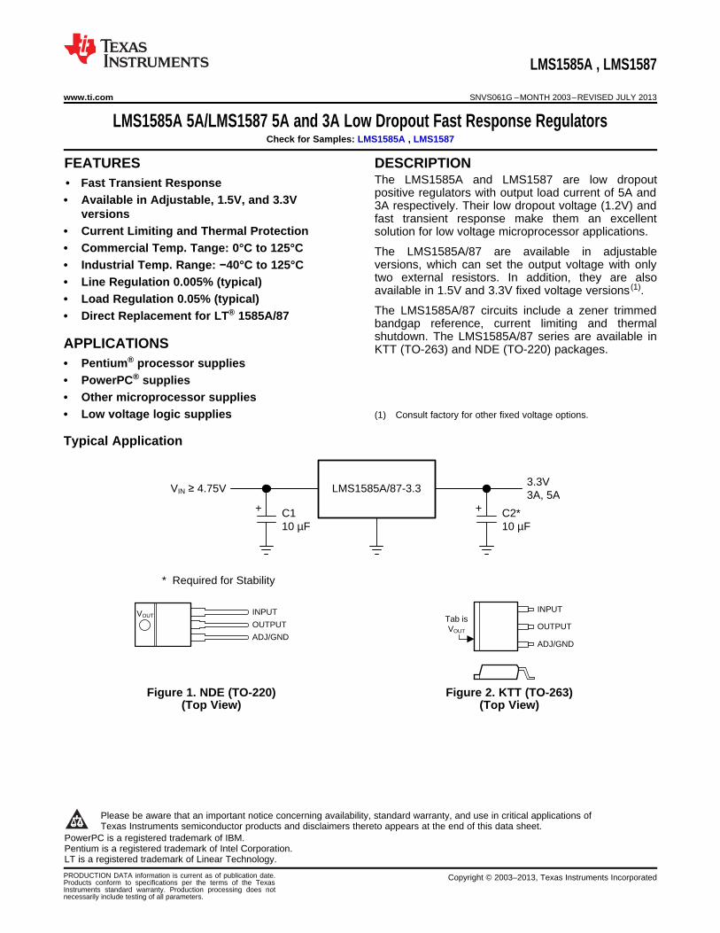
LMS1585A/87-3.3VIN 4.75V3.3V3A, 5A
+ + C2*10 µF
C110 µF
* Required for Stability
LMS1585A , LMS1587
www.ti.com SNVS061G –MONTH 2003–REVISED JULY 2013
LMS1585A 5A/LMS1587 5A and 3A Low Dropout Fast Response RegulatorsCheck for Samples: LMS1585A , LMS1587
1FEATURES DESCRIPTIONThe LMS1585A and LMS1587 are low dropout
234• Fast Transient Responsepositive regulators with output load current of 5A and• Available in Adjustable, 1.5V, and 3.3V 3A respectively. Their low dropout voltage (1.2V) and
versions fast transient response make them an excellent• Current Limiting and Thermal Protection solution for low voltage microprocessor applications.• Commercial Temp. Tange: 0°C to 125°C The LMS1585A/87 are available in adjustable
versions, which can set the output voltage with only• Industrial Temp. Range: −40°C to 125°Ctwo external resistors. In addition, they are also• Line Regulation 0.005% (typical)available in 1.5V and 3.3V fixed voltage versions (1).
• Load Regulation 0.05% (typical)The LMS1585A/87 circuits include a zener trimmed• Direct Replacement for LT® 1585A/87 bandgap reference, current limiting and thermalshutdown. The LMS1585A/87 series are available inAPPLICATIONS KTT (TO-263) and NDE (TO-220) packages.
• Pentium® processor supplies• PowerPC® supplies• Other microprocessor supplies• Low voltage logic supplies (1) Consult factory for other fixed voltage options.
Typical Application
Figure 1. NDE (TO-220) Figure 2. KTT (TO-263)(Top View) (Top View)
1
Please be aware that an important notice concerning availability, standard warranty, and use in critical applications ofTexas Instruments semiconductor products and disclaimers thereto appears at the end of this data sheet.
2PowerPC is a registered trademark of IBM.3Pentium is a registered trademark of Intel Corporation.4LT is a registered trademark of Linear Technology.PRODUCTION DATA information is current as of publication date. Copyright © 2003–2013, Texas Instruments IncorporatedProducts conform to specifications per the terms of the TexasInstruments standard warranty. Production processing does notnecessarily include testing of all parameters.
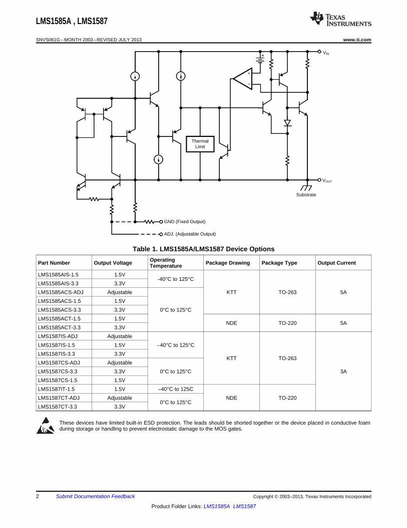
ThermalLimit
VIN
VOUT
Substrate
GND (Fixed Output)
tADJ. (Adjustable Output)ttt
LMS1585A , LMS1587
SNVS061G –MONTH 2003–REVISED JULY 2013 www.ti.com
Table 1. LMS1585A/LMS1587 Device OptionsOperatingPart Number Output Voltage Package Drawing Package Type Output CurrentTemperature
LMS1585AIS-1.5 1.5V-40°C to 125°C
LMS1585AIS-3.3 3.3VLMS1585ACS-ADJ Adjustable KTT TO-263 5ALMS1585ACS-1.5 1.5VLMS1585ACS-3.3 3.3V 0°C to 125°CLMS1585ACT-1.5 1.5V
NDE TO-220 5ALMS1585ACT-3.3 3.3VLMS1587IS-ADJ AdjustableLMS1587IS-1.5 1.5V –40°C to 125°CLMS1587IS-3.3 3.3V
KTT TO-263LMS1587CS-ADJ AdjustableLMS1587CS-3.3 3.3V 0°C to 125°C 3ALMS1587CS-1.5 1.5VLMS1587IT-1.5 1.5V –40°C to 125CLMS1587CT-ADJ Adjustable NDE TO-220
0°C to 125°CLMS1587CT-3.3 3.3V
These devices have limited built-in ESD protection. The leads should be shorted together or the device placed in conductive foamduring storage or handling to prevent electrostatic damage to the MOS gates.
2 Submit Documentation Feedback Copyright © 2003–2013, Texas Instruments Incorporated
Product Folder Links: LMS1585A LMS1587
LMS1585A , LMS1587
www.ti.com SNVS061G –MONTH 2003–REVISED JULY 2013
ABSOLUTE MAXIMUM RATINGS (1) (2)
Maximum Input to Output Voltage (VIN to GND) 13VPower Dissipation (3) Internally LimitedJunction Temperature (TJ) (3) 150˚CStorage Temperature Range -65˚C to 150˚CLead Temperature 260˚C, 10 secESD Tolerance (4) 2000V
(1) Absolute Maximum Ratings indicate limits beyond which damage to the device may occur. Operating Ratings indicate conditions forwhich the device is intended to be functional, but specific performance is not ensured. For ensured specifications and the testconditions, see the Electrical Characteristics.
(2) If Military/Aerospace specified devices are required, please contact the TI Sales Office/ Distributors for availability and specifications.(3) The maximum power dissipation is a function of TJ(max) , θJA, and TA. The maximum allowable power dissipation at any ambient
temperature is PD = (TJ(max)–T A)/θJA. All numbers apply for packages soldered directly into a PC board.(4) For testing purposes, ESD was applied using human body model, 1.5 kΩ in series with 100 pF.
Copyright © 2003–2013, Texas Instruments Incorporated Submit Documentation Feedback 3
Product Folder Links: LMS1585A LMS1587
LMS1585A , LMS1587
SNVS061G –MONTH 2003–REVISED JULY 2013 www.ti.com
ELECTRICAL CHARACTERISTICSTypicals and limits appearing in normal type apply for TJ = 25˚C. Limits appearing in Boldface type apply over the entirejunction temperature range for operation, 0˚C to 125˚C for commercial grade and −40˚C to 125˚C for industrial grade.
Symbol Parameter Conditions Min (1) Typ (2) Max (1) UnitsVREF Reference Voltage LMS1585A-ADJ
VIN−VOUT = 3V, IOUT = 10mA 1.238 1.250 1.262 V10mA ≤ IOUT ≤ 5A, 1.5V ≤ VIN− VOUT ≤ 5.75V 1.225 1.250 1.275 VLMS1587-ADJ10mA ≤ IOUT ≤ 3A, 1.5V ≤ VIN−VOUT ≤ 5.75V 1.225 1.250 1.275 V
VOUT Output Voltage LMS1585A-1.5IOUT = 0mA, VIN = 5V 1.485 1.500 1.515 V0 ≤ IOUT ≤ 5A, 3V ≤ VIN ≤ 7V 1.470 1.530 VLMS1585A-3.3I OUT = 0mA, V IN = 5V 3.267 3.300 3.333 V0 ≤ I OUT ≤ 5A, 4.75V ≤ V IN ≤ 7V 3.235 3.300 3.365 VLMS1587-1.5V IN = 5V, I OUT = 0mA, TJ = 25˚C 1.485 1.500 1.515 V0≤ I OUT ≤ 3A, 3V ≤ VIN ≤ 7V 1.470 1.500 1.530 VLMS1587-3.30 ≤ I OUT ≤ 3A, 4.75V ≤ VIN ≤ 7V 3.235 3.300 3.365 V
∆VOUT Line Regulation (3) LMS1585A/87-ADJIOUT = 10mA, 2.75V ≤ V IN ≤ 7V 0.005 0.2 %LMS1585A/87-3.3I OUT = 0mA, 4.75V ≤ VIN ≤ 7V 0.005 0.2 %LMS1585A/87-1.5I OUT = 0mA, 3V ≤ VIN ≤ 7V 0.005 0.2 %
∆VOUT Load Regulation (3) LMS1585A-ADJ 0.3 %VIN−VOUT = 3V, 10mA ≤ IOUT ≤ 5A 0.05 0.5LMS1585A-1.5/LMS1585A-3.3 0.05 0.3 %VIN = 5V, 0 ≤ IOUT ≤ 5A 0.05 0.5LMS1587-ADJ 0.05 0.3VIN−VOUT = 3V, 10mA ≤ IOUT ≤ 3A 0.05 0.5 %LMS1587-1.5/LMS1587-3.3 0.05 0.3 %VIN = 5V, 0 ≤ IOUT ≤ 3A 0.05 0.5 %
VIN−VOUT Dropout Voltage LMS1585A-ADJ/LMS1587-ADJ∆VREF = 1%, IOUT = 3A 1.15 1.3 VLMS1585A-3.3/LMS1587-3.3/LMS1585A-1.5/LMS1587-1.5∆VOUT = 1%, IOUT = 3A 1.15 1.3 VLMS1585A-ADJ∆VREF = 1%, IOUT = 5A 1.2 1.4 VLMS1585A-1.5/LMS1585A-3.3∆VOUT = 1%, IOUT = 5A 1.2 1.4 V
(1) All limits are specified by testing or statistical analysis.(2) Typical Values represent the most likely parametric norm.(3) Load and line regulation are measured at constant junction temperature, and are ensured up to the maximum power dissipation of 30W.
Power dissipation is determined by the input/output differential and the output current. Ensured maximum power dissipation will not beavailable over the full input/output range.
4 Submit Documentation Feedback Copyright © 2003–2013, Texas Instruments Incorporated
Product Folder Links: LMS1585A LMS1587

LMS1585A , LMS1587
www.ti.com SNVS061G –MONTH 2003–REVISED JULY 2013
ELECTRICAL CHARACTERISTICS (continued)Typicals and limits appearing in normal type apply for TJ = 25˚C. Limits appearing in Boldface type apply over the entirejunction temperature range for operation, 0˚C to 125˚C for commercial grade and −40˚C to 125˚C for industrial grade.ILIMIT Current Limit LMS1585A-ADJ/LMS1585A-3.3/LMS1585A-1.5
VIN−VOUT = 5.5V 5.0 6.6 ALMS1587-ADJ/LMS1587-3.3/LMS1587-1.5VIN−VOUT = 5.5V 3.1 4.3 A
Minimum Load LMS1585A/87-ADJCurrent (4) 1.5V ≤ VIN−VOUT ≤ 5.75V 2.0 10.0 mAQuiescent Current LMS1585A-3.3/LMS1587-3.3/
LMS1585A-1.5/LMS1587-1.5VIN = 5V 7.0 13.0 mA
Thermal Regulation TA = 25˚C, 30ms Pulse 0.003 %/WRipple Rejection LMS1585A-ADJ
fRIPPLE = 120Hz, VIN−VOUT = 3V,IOUT = 5A, COUT = 25µF Tantalum 72 dBLMS1585A-1.5fRIPPLE = 120Hz, COUT = 25µFTantalum, IOUT = 5A, VIN = 4.5V 60 72 dBLMS1585A-3.3fRIPPLE = 120Hz, COUT = 25µFTantalum, IOUT = 5A, VIN = 6.3V 72 dBLMS1587-ADJfRIPPLE = 120 Hz, VIN−VOUT = 3V, IOUT = 3ACOUT = 25 µF Tantalum 72 dBLMS1587-1.5fRIPPLE = 120 Hz, COUT = 25µF Tantalum,IOUT = 3A, VIN = 4.5V 60 72 dBLMS1587-3.3fRIPPLE = 120 Hz, COUT = 25µF Tantalum,IOUT = 3A, VIN = 6.3V 72 dB
Adjust Pin Current 55 120 µAAdjust Pin Current 10mA ≤ IOUT ≤ IFULLLOAD,
1.5V ≤ VIN−VOUT ≤ 5.75V (5) 0.2 µATemperature Stability 0.5 %Long Term Stability TA = 125˚C, 1000Hrs 0.03 %RMS Output Noise 10Hz ≤ f ≤ 10kHz 0.003 %(% of VOUT)Thermal Resistance 3-Lead KTT (TO-263): Control/Output Section 0.65/2.7 *C/WJunction-to-Case 3-Lead NDE (TO-220): Control/Output Section 0.65/2.7 *C/W
(4) The minimum output current required to maintain regulation.(5) IFULLLOAD is 5A for LMS1585A and 3A for LMS1587.
Copyright © 2003–2013, Texas Instruments Incorporated Submit Documentation Feedback 5
Product Folder Links: LMS1585A LMS1587

VOUTVIN
I1
10 µF
VREF
10 µF
R1
R2IADJ
VIN VOUT
ADJ
VOUT = VREF (1 + R2) + IADJR2R2
R1
LMS1585A , LMS1587
SNVS061G –MONTH 2003–REVISED JULY 2013 www.ti.com
APPLICATION NOTE
OUTPUT VOLTAGE
The adjustable version develops at 1.25V reference voltage, (VREF), between the output and the adjust terminal.As shown in Figure 3, this voltage is applied across resistor R1 to generate a constant current I1. This constantcurrent then flows through R2. The resulting voltage drop across R2 adds to the reference voltage to sets thedesired output voltage.
The current IADJ from the adjustment terminal introduces an output error. But since it is small (120μA max), itbecomes negligible when R1 is in the 100Ω range.
For fixed voltage devices, R1 and R2 are integrated inside the devices.
Figure 3. Basic Adjustable Regulator
6 Submit Documentation Feedback Copyright © 2003–2013, Texas Instruments Incorporated
Product Folder Links: LMS1585A LMS1587
PACKAGE OPTION ADDENDUM
www.ti.com 6-Feb-2020
Addendum-Page 1
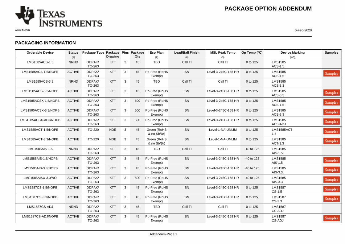
PACKAGING INFORMATION
Orderable Device Status(1)
Package Type PackageDrawing
Pins PackageQty
Eco Plan(2)
Lead/Ball Finish(6)
MSL Peak Temp(3)
Op Temp (°C) Device Marking(4/5)
Samples
LMS1585ACS-1.5 NRND DDPAK/TO-263
KTT 3 45 TBD Call TI Call TI 0 to 125 LMS1585ACS-1.5
LMS1585ACS-1.5/NOPB ACTIVE DDPAK/TO-263
KTT 3 45 Pb-Free (RoHSExempt)
SN Level-3-245C-168 HR 0 to 125 LMS1585ACS-1.5
LMS1585ACS-3.3 NRND DDPAK/TO-263
KTT 3 45 TBD Call TI Call TI 0 to 125 LMS1585ACS-3.3
LMS1585ACS-3.3/NOPB ACTIVE DDPAK/TO-263
KTT 3 45 Pb-Free (RoHSExempt)
SN Level-3-245C-168 HR 0 to 125 LMS1585ACS-3.3
LMS1585ACSX-1.5/NOPB ACTIVE DDPAK/TO-263
KTT 3 500 Pb-Free (RoHSExempt)
SN Level-3-245C-168 HR 0 to 125 LMS1585ACS-1.5
LMS1585ACSX-3.3/NOPB ACTIVE DDPAK/TO-263
KTT 3 500 Pb-Free (RoHSExempt)
SN Level-3-245C-168 HR 0 to 125 LMS1585ACS-3.3
LMS1585ACSX-ADJ/NOPB ACTIVE DDPAK/TO-263
KTT 3 500 Pb-Free (RoHSExempt)
SN Level-3-245C-168 HR 0 to 125 LMS1585ACS-ADJ
LMS1585ACT-1.5/NOPB ACTIVE TO-220 NDE 3 45 Green (RoHS& no Sb/Br)
SN Level-1-NA-UNLIM 0 to 125 LMS1585ACT1.5
LMS1585ACT-3.3/NOPB ACTIVE TO-220 NDE 3 45 Green (RoHS& no Sb/Br)
SN Level-1-NA-UNLIM 0 to 125 LMS1585ACT-3.3
LMS1585AIS-1.5 NRND DDPAK/TO-263
KTT 3 45 TBD Call TI Call TI -40 to 125 LMS1585AIS-1.5
LMS1585AIS-1.5/NOPB ACTIVE DDPAK/TO-263
KTT 3 45 Pb-Free (RoHSExempt)
SN Level-3-245C-168 HR -40 to 125 LMS1585AIS-1.5
LMS1585AIS-3.3/NOPB ACTIVE DDPAK/TO-263
KTT 3 45 Pb-Free (RoHSExempt)
SN Level-3-245C-168 HR -40 to 125 LMS1585AIS-3.3
LMS1585AISX-3.3/NO ACTIVE DDPAK/TO-263
KTT 3 500 Pb-Free (RoHSExempt)
SN Level-3-245C-168 HR -40 to 125 LMS1585AIS-3.3
LMS1587CS-1.5/NOPB ACTIVE DDPAK/TO-263
KTT 3 45 Pb-Free (RoHSExempt)
SN Level-3-245C-168 HR 0 to 125 LMS1587CS-1.5
LMS1587CS-3.3/NOPB ACTIVE DDPAK/TO-263
KTT 3 45 Pb-Free (RoHSExempt)
SN Level-3-245C-168 HR 0 to 125 LMS1587CS-3.3
LMS1587CS-ADJ NRND DDPAK/TO-263
KTT 3 45 TBD Call TI Call TI 0 to 125 LMS1587CS-ADJ
LMS1587CS-ADJ/NOPB ACTIVE DDPAK/TO-263
KTT 3 45 Pb-Free (RoHSExempt)
SN Level-3-245C-168 HR 0 to 125 LMS1587CS-ADJ

PACKAGE OPTION ADDENDUM
www.ti.com 6-Feb-2020
Addendum-Page 2
Orderable Device Status(1)
Package Type PackageDrawing
Pins PackageQty
Eco Plan(2)
Lead/Ball Finish(6)
MSL Peak Temp(3)
Op Temp (°C) Device Marking(4/5)
Samples
LMS1587CSX-1.5/NOPB ACTIVE DDPAK/TO-263
KTT 3 500 Pb-Free (RoHSExempt)
SN Level-3-245C-168 HR 0 to 125 LMS1587CS-1.5
LMS1587CSX-3.3/NOPB ACTIVE DDPAK/TO-263
KTT 3 500 Pb-Free (RoHSExempt)
SN Level-3-245C-168 HR 0 to 125 LMS1587CS-3.3
LMS1587CSX-ADJ/NOPB ACTIVE DDPAK/TO-263
KTT 3 500 Pb-Free (RoHSExempt)
SN Level-3-245C-168 HR 0 to 125 LMS1587CS-ADJ
LMS1587CT-3.3 NRND TO-220 NDE 3 45 TBD Call TI Call TI 0 to 125 LMS1587CT-3.3
LMS1587CT-3.3/NOPB ACTIVE TO-220 NDE 3 45 Green (RoHS& no Sb/Br)
SN Level-1-NA-UNLIM 0 to 125 LMS1587CT-3.3
LMS1587CT-ADJ/NOPB ACTIVE TO-220 NDE 3 45 Green (RoHS& no Sb/Br)
SN Level-1-NA-UNLIM 0 to 125 LMS1587CT-ADJ
LMS1587IS-1.5 NRND DDPAK/TO-263
KTT 3 45 TBD Call TI Call TI -40 to 125 LMS1587IS-1.5
LMS1587IS-1.5/NOPB ACTIVE DDPAK/TO-263
KTT 3 45 Pb-Free (RoHSExempt)
SN Level-3-245C-168 HR -40 to 125 LMS1587IS-1.5
LMS1587IS-3.3 NRND DDPAK/TO-263
KTT 3 45 TBD Call TI Call TI -40 to 125 LMS1587IS-3.3
LMS1587IS-3.3/NOPB ACTIVE DDPAK/TO-263
KTT 3 45 Pb-Free (RoHSExempt)
SN Level-3-245C-168 HR -40 to 125 LMS1587IS-3.3
LMS1587IS-ADJ NRND DDPAK/TO-263
KTT 3 45 TBD Call TI Call TI -40 to 125 LMS1587IS-ADJ
LMS1587IS-ADJ/NOPB ACTIVE DDPAK/TO-263
KTT 3 45 Pb-Free (RoHSExempt)
SN Level-3-245C-168 HR -40 to 125 LMS1587IS-ADJ
LMS1587ISX-3.3/NOPB ACTIVE DDPAK/TO-263
KTT 3 500 Pb-Free (RoHSExempt)
SN Level-3-245C-168 HR -40 to 125 LMS1587IS-3.3
LMS1587ISX-ADJ/NOPB ACTIVE DDPAK/TO-263
KTT 3 500 Pb-Free (RoHSExempt)
SN Level-3-245C-168 HR -40 to 125 LMS1587IS-ADJ
LMS1587IT-1.5/NOPB ACTIVE TO-220 NDE 3 45 Green (RoHS& no Sb/Br)
SN Level-1-NA-UNLIM -40 to 125 LMS1587IT-1.5
(1) The marketing status values are defined as follows:ACTIVE: Product device recommended for new designs.LIFEBUY: TI has announced that the device will be discontinued, and a lifetime-buy period is in effect.NRND: Not recommended for new designs. Device is in production to support existing customers, but TI does not recommend using this part in a new design.PREVIEW: Device has been announced but is not in production. Samples may or may not be available.OBSOLETE: TI has discontinued the production of the device.

PACKAGE OPTION ADDENDUM
www.ti.com 6-Feb-2020
Addendum-Page 3
(2) RoHS: TI defines "RoHS" to mean semiconductor products that are compliant with the current EU RoHS requirements for all 10 RoHS substances, including the requirement that RoHS substancedo not exceed 0.1% by weight in homogeneous materials. Where designed to be soldered at high temperatures, "RoHS" products are suitable for use in specified lead-free processes. TI mayreference these types of products as "Pb-Free".RoHS Exempt: TI defines "RoHS Exempt" to mean products that contain lead but are compliant with EU RoHS pursuant to a specific EU RoHS exemption.Green: TI defines "Green" to mean the content of Chlorine (Cl) and Bromine (Br) based flame retardants meet JS709B low halogen requirements of <=1000ppm threshold. Antimony trioxide basedflame retardants must also meet the <=1000ppm threshold requirement.
(3) MSL, Peak Temp. - The Moisture Sensitivity Level rating according to the JEDEC industry standard classifications, and peak solder temperature.
(4) There may be additional marking, which relates to the logo, the lot trace code information, or the environmental category on the device.
(5) Multiple Device Markings will be inside parentheses. Only one Device Marking contained in parentheses and separated by a "~" will appear on a device. If a line is indented then it is a continuationof the previous line and the two combined represent the entire Device Marking for that device.
(6) Lead/Ball Finish - Orderable Devices may have multiple material finish options. Finish options are separated by a vertical ruled line. Lead/Ball Finish values may wrap to two lines if the finishvalue exceeds the maximum column width.
Important Information and Disclaimer:The information provided on this page represents TI's knowledge and belief as of the date that it is provided. TI bases its knowledge and belief on informationprovided by third parties, and makes no representation or warranty as to the accuracy of such information. Efforts are underway to better integrate information from third parties. TI has taken andcontinues to take reasonable steps to provide representative and accurate information but may not have conducted destructive testing or chemical analysis on incoming materials and chemicals.TI and TI suppliers consider certain information to be proprietary, and thus CAS numbers and other limited information may not be available for release.
In no event shall TI's liability arising out of such information exceed the total purchase price of the TI part(s) at issue in this document sold by TI to Customer on an annual basis.
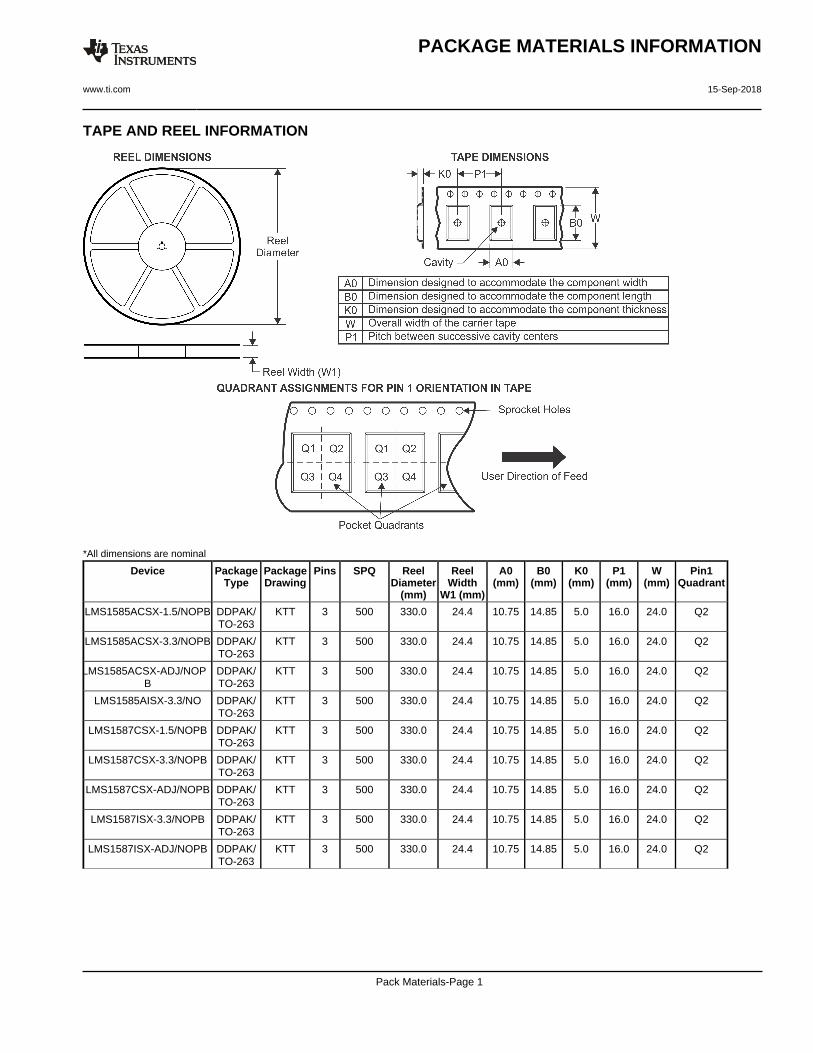
TAPE AND REEL INFORMATION
*All dimensions are nominal
Device PackageType
PackageDrawing
Pins SPQ ReelDiameter
(mm)
ReelWidth
W1 (mm)
A0(mm)
B0(mm)
K0(mm)
P1(mm)
W(mm)
Pin1Quadrant
LMS1585ACSX-1.5/NOPB DDPAK/TO-263
KTT 3 500 330.0 24.4 10.75 14.85 5.0 16.0 24.0 Q2
LMS1585ACSX-3.3/NOPB DDPAK/TO-263
KTT 3 500 330.0 24.4 10.75 14.85 5.0 16.0 24.0 Q2
LMS1585ACSX-ADJ/NOPB
DDPAK/TO-263
KTT 3 500 330.0 24.4 10.75 14.85 5.0 16.0 24.0 Q2
LMS1585AISX-3.3/NO DDPAK/TO-263
KTT 3 500 330.0 24.4 10.75 14.85 5.0 16.0 24.0 Q2
LMS1587CSX-1.5/NOPB DDPAK/TO-263
KTT 3 500 330.0 24.4 10.75 14.85 5.0 16.0 24.0 Q2
LMS1587CSX-3.3/NOPB DDPAK/TO-263
KTT 3 500 330.0 24.4 10.75 14.85 5.0 16.0 24.0 Q2
LMS1587CSX-ADJ/NOPB DDPAK/TO-263
KTT 3 500 330.0 24.4 10.75 14.85 5.0 16.0 24.0 Q2
LMS1587ISX-3.3/NOPB DDPAK/TO-263
KTT 3 500 330.0 24.4 10.75 14.85 5.0 16.0 24.0 Q2
LMS1587ISX-ADJ/NOPB DDPAK/TO-263
KTT 3 500 330.0 24.4 10.75 14.85 5.0 16.0 24.0 Q2
PACKAGE MATERIALS INFORMATION
www.ti.com 15-Sep-2018
Pack Materials-Page 1

*All dimensions are nominal
Device Package Type Package Drawing Pins SPQ Length (mm) Width (mm) Height (mm)
LMS1585ACSX-1.5/NOPB DDPAK/TO-263 KTT 3 500 367.0 367.0 45.0
LMS1585ACSX-3.3/NOPB DDPAK/TO-263 KTT 3 500 367.0 367.0 45.0
LMS1585ACSX-ADJ/NOPB
DDPAK/TO-263 KTT 3 500 367.0 367.0 45.0
LMS1585AISX-3.3/NO DDPAK/TO-263 KTT 3 500 367.0 367.0 45.0
LMS1587CSX-1.5/NOPB DDPAK/TO-263 KTT 3 500 367.0 367.0 45.0
LMS1587CSX-3.3/NOPB DDPAK/TO-263 KTT 3 500 367.0 367.0 45.0
LMS1587CSX-ADJ/NOPB DDPAK/TO-263 KTT 3 500 367.0 367.0 45.0
LMS1587ISX-3.3/NOPB DDPAK/TO-263 KTT 3 500 367.0 367.0 45.0
LMS1587ISX-ADJ/NOPB DDPAK/TO-263 KTT 3 500 367.0 367.0 45.0
PACKAGE MATERIALS INFORMATION
www.ti.com 15-Sep-2018
Pack Materials-Page 2

MECHANICAL DATA
NDE0003B
www.ti.com

MECHANICAL DATA
KTT0003B
www.ti.com
BOTTOM SIDE OF PACKAGETS3B (Rev F)
IMPORTANT NOTICE AND DISCLAIMER
TI PROVIDES TECHNICAL AND RELIABILITY DATA (INCLUDING DATASHEETS), DESIGN RESOURCES (INCLUDING REFERENCE DESIGNS), APPLICATION OR OTHER DESIGN ADVICE, WEB TOOLS, SAFETY INFORMATION, AND OTHER RESOURCES “AS IS” AND WITH ALL FAULTS, AND DISCLAIMS ALL WARRANTIES, EXPRESS AND IMPLIED, INCLUDING WITHOUT LIMITATION ANY IMPLIED WARRANTIES OF MERCHANTABILITY, FITNESS FOR A PARTICULAR PURPOSE OR NON-INFRINGEMENT OF THIRD PARTY INTELLECTUAL PROPERTY RIGHTS.These resources are intended for skilled developers designing with TI products. You are solely responsible for (1) selecting the appropriate TI products for your application, (2) designing, validating and testing your application, and (3) ensuring your application meets applicable standards, and any other safety, security, or other requirements. These resources are subject to change without notice. TI grants you permission to use these resources only for development of an application that uses the TI products described in the resource. Other reproduction and display of these resources is prohibited. No license is granted to any other TI intellectual property right or to any third party intellectual property right. TI disclaims responsibility for, and you will fully indemnify TI and its representatives against, any claims, damages, costs, losses, and liabilities arising out of your use of these resources.TI’s products are provided subject to TI’s Terms of Sale (www.ti.com/legal/termsofsale.html) or other applicable terms available either on ti.com or provided in conjunction with such TI products. TI’s provision of these resources does not expand or otherwise alter TI’s applicable warranties or warranty disclaimers for TI products.
Mailing Address: Texas Instruments, Post Office Box 655303, Dallas, Texas 75265Copyright © 2020, Texas Instruments Incorporated