lo4 - defense technical information center · lo4 implementation of ... et les syst~mes...
TRANSCRIPT
I National DefenseDetence nationale
DT"CS : JAN 301091 4
Lo4
IMPLEMENTATION OF FFT AND PULSECOMPRESSION ROUTINES ON THE SPT
FREQUENCY DOMAIN ARRAY PROCESSORby
V. Behroozi and A. Damini
uzx UDnkaI'ad
'-'
DEFENCE RESEARCH ESTABLISHMENT OTTAWAREPORT NO.1041
September 1990Ottawa91 1 29 044
National DefenseU Defence nalonale
IMPLEMENTATION OF FFT AND PULSECOMPRESSION ROUTINES ON THE SPT
FREQUENCY DOMAIN ARRAY PROCESSORby
V. Behroozi and A. DamiAirborne Rada~r Section
RadarDivisiOn
DEFENCE RESEARCH ESTABLISHMENT OTTAWAREPORT NO.1 041
PCN September 1990021 LA Ottawa
ABSTRACT
The Frequency Domain Array Processor (FDAP) is a VME compatible circuit boardbuilt by Signal Processing Technologies (SPT). The FDAP can process integer data arrayscontaining up to 8192 (32 bit) complex words or 16384 (16 bit) real words. It is capable of400 Million Operations Per Second (MOPS) with a maximum Input/Output (I/O) rate offour billion bits per second. It also has a double buffered memory architecture permittingI/O transfers to occur in parallel with data processing. The FDAP can be hosted by anIBM PC/AT-compatible computer using a bus adaptor interface available from BIT3Computer Corp.
The FDAP board is based upon SPT's DASP/PAC chip set. This chip set and thevarious system architectures which can be built around it are reviewed. The FDAP boardand its associated development system are also reviewed. The ease of implementation oftypical radar signal processing functions on the FDAP board are then examined. FastFourier Transform and pulse compression rouzines are implemented via a supplied userinterface as weil as a high level language (C). The results are examined and comments onthe FDAP and its associated system development tools are made.
RtSUME
Le Processeur Parallle dans le Domaine des Fr~quences, (PPDF) est une carte6lectronique compatible avec VME fabriqu6e par Signal Processing Technologies (SPT).Le PPDF peut traiter des vecteurs de donn6es entires contenant jusqu'A 8192 (32 bits)codes complexes ou 16384 (16 bits) codes r6els. I] est capable de r6aliser 400 MillionsOperations Par Seconde (MOPS) avec un taux maximum d'Entr6e/Sortie (E/S) de quatremilliards de bits par seconde. I1 poss~de aussi deux m~moires tampons permettant letraitement et la transmission de donn6es simultan6ment. Le PPDF fonctionne sur unordinateur compatible avec un IBM PC/AT A I'aide d'une interface adaptive bus disponiblechcz la corporation BIT3 Computer.
La carte PPDF est bas6e sur la famille de puces DASP/PAC de SPT. Cette familleet les syst~mes d'architecture vari6s qui peuvent y tre associ6s sont revis6s. La facilit6d'implantation de fonctions typiques d'analyse de signaux radars sur la carte PPDF estensuite exainin6e. Les transformfes de Fourier Rapides et routines de compressiond'impulsions sont implant6s par l'usager via une interface et un haut niveau de langage (C).Les r~suliats sont examin6s et la carte PPDF, ainsi que les outils de d~veloppement desyst~me qui lui sont associ6s, sont comment6s.
iii/iv
EXECUTIVE SUMMARY
State of the art Synthetic Aperture Radars (SAR) transmit high bandwidth pulses andsubsequently require extremely high sampling rates. The processing rates required toaccommodate the resulting data rates are also very high. The advances in board levelproducts for high-speed standard busses has reached the point where it may be possible toreplace current processors with ones occupying much smaller volumes, which are moresuitable for an airborne environment. This report examines the use of one such card forapplication to a subset of operations required in such processors.
The board-level processor examined in this study is the Frequency i)V'Ti, Arra',P",'essor (FDAP), a V ME compatible circuit board built by Signal Processing Technologies(SPT). The FDAP can process integer data arrays containing up to 8192 (32 bit) complexwords or 16384 (16 bit) real words. It is capable of 400 Million Operations Per Second(MOPS) with a maximum I/O rate of four billion bits per second. The FDAP board isbased upon SPT's DASP/PAC chip set. This chip set and the various system architectureswhich can be built around it are reviewed. The FDAP board and its associateddevelopment system are also reviewed. The ease of implementation of typical radar signalprocessing functions on the FDAP board are then examined. Fast Fourier Transform andpulse compression routines are implemented via a supplied user interface as well as a highlevel language (C). The results are examined and comments on the FDAP and itsassociated system development tools are made.
v/vi
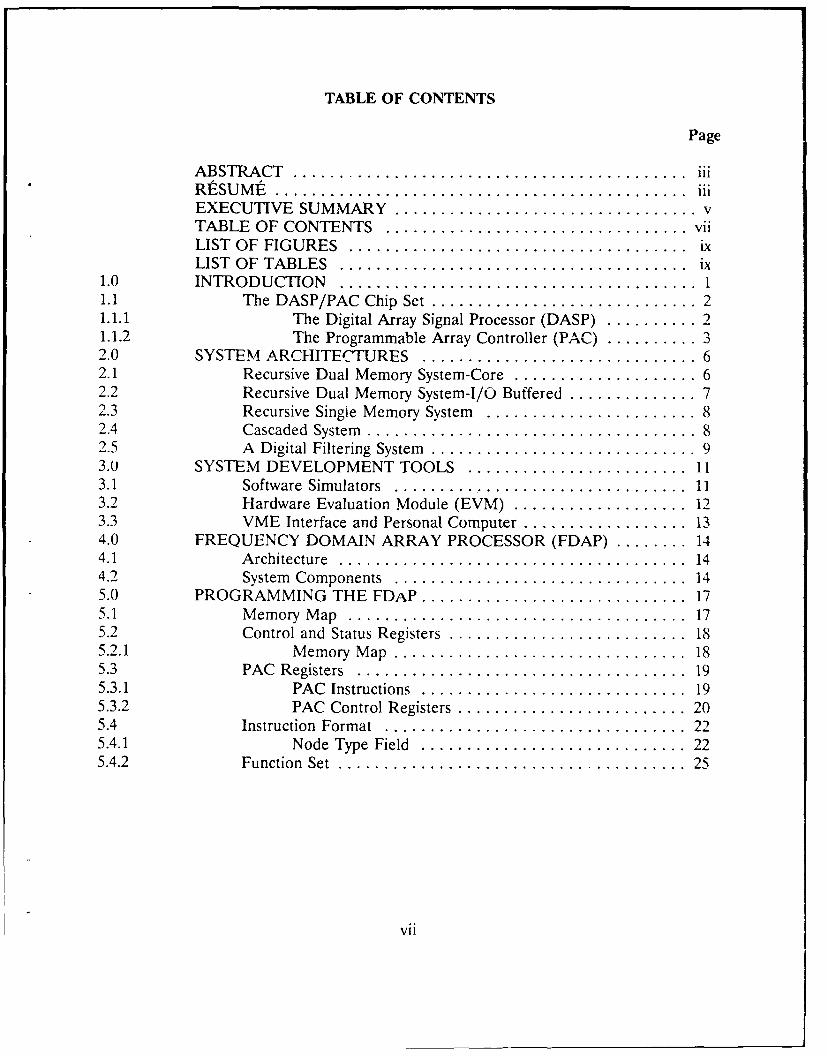
TABLE OF CONTENTS
Page
A BSTRA CT ........................................... iiiR tSU M t. ............................................. iiiEXECUTIVE SUMMARY ................................. vTABLE OF CONTENTS ................................. viiLIST OF FIGURES ..................................... ixLIST OF TABLES ...................................... ix
1.0 INTRODUCTION ....................................... 11.1 The DASP/PAC Chip Set ............................. 21.1.1 The Digital Array Signal Processor (DASP) .......... 21.1.2 The Programmable Array Controller (PAC) .......... 32.0 SYSTEM ARCHITECTURES .............................. 62.1 Recursive Dual Memory System-Core .................... 62.2 Recursive Dual Memory System-I/O Buffered .............. 72.3 Recursive Single Memory System ....................... 82.4 Cascaded System .................................... 82.5 A Digital Filtering System ............................. 93.0 SYSTEM DEVELOPMENT TOOLS ........................ 113.1 Software Simulators ................................. 113.2 Hardware Evaluation Module (EVM) ................... 123.3 VME Interface and Personal Computer .................. 134.0 FREQUENCY DOMAIN ARRAY PROCESSOR (FDAP) ........ 144.1 A rchitecture ...................................... 144.2 System Components ................................ 145.0 PROGRAMMING THE FDAP ............................. 175.1 M em ory M ap ..................................... 175.2 Control and Status Registers .......................... 185.2.1 M em ory M ap ................................ 185.3 PAC Registers .................................... 195.3.1 PAC Instructions ............................. 195.3.2 PAC Control Registers ......................... 205.4 Instruction Form at ................................. 225.4.1 Node Type Field ............................. 225.4.2 Function Set ...................................... 25
vii
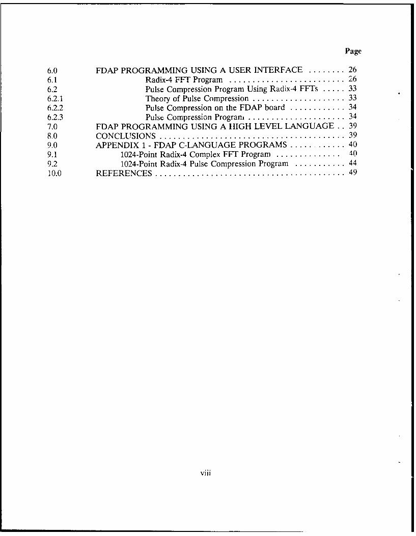
Page
6.0 FDAP PROGRAMMING USING A USER INTERFACE ........ 266.1 Radix-4 FFT Program .......................... 266.2 Pulse Compression Program Using Radix-4 FFTs ..... 336.2.1 Theory of Pulse Compression .................... 336.2.2 Pulse Compression on the FDAP board ............ 346.2.3 Pulse Compression Program ..................... 347.0 FDAP PROGRAMMING USING A HIGH LEVEL LANGUAGE .. 398.0 CONCLUSIONS ........................................ 399.0 APPENDIX 1 - FDAP C-LANGUAGE PROGRAMS ............ 409.1 1024-Point Radix-4 Complex FFT Program .............. V)9.2 1024-Point Radix-4 Pulse Compression Program ........... 4410.0 REFERENCES ......................................... 49
viii
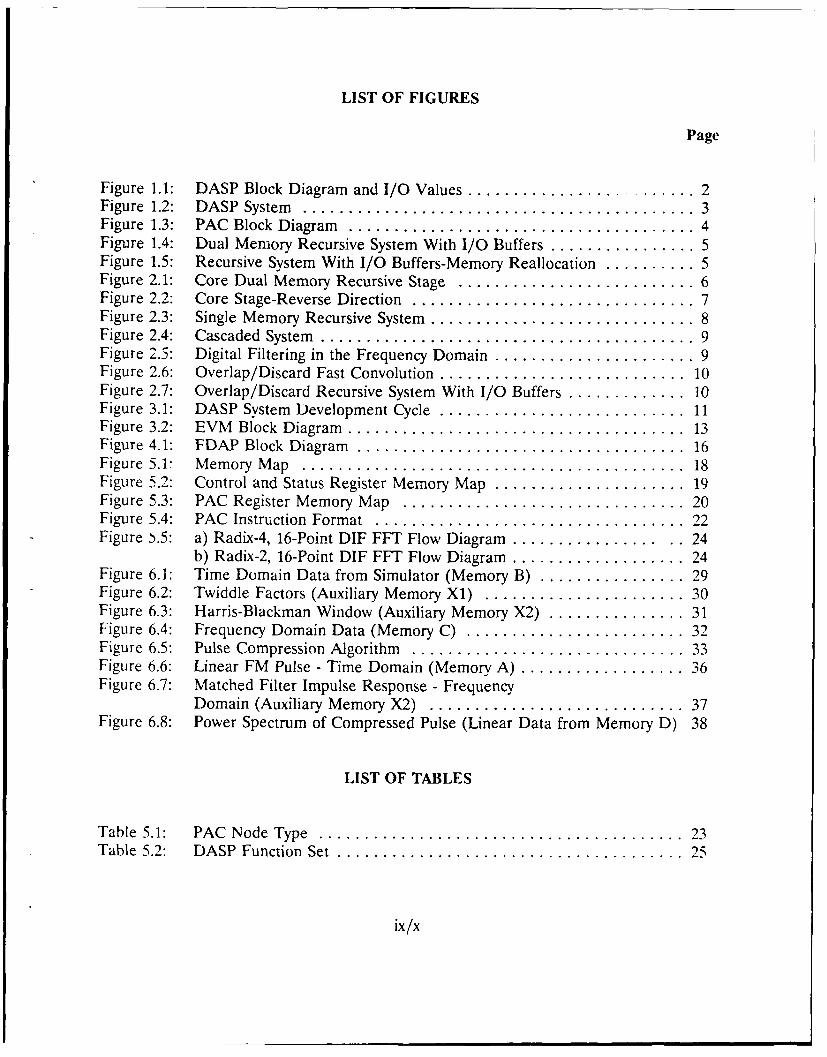
LIST OF FIGURES
Page
Figure 1.1: DASP Block Diagram and I/O Values ......................... 2Figure 1.2: DASP System ........................................... 3Figure 1.3: PAC Block Diagram ...................................... 4Figure 1.4: Dual Memory Recursive System With I/O Buffers ................ 5Figure 1.5: Recursive System With I/O Buffers-Memory Reallocation .......... 5Figure 2.1: Core Dual Memory Recursive Stage .......................... 6Figure 2.2: Core Stage-Reverse Direction ............................... 7Figure 2.3: Single Memory Recursive System ............................. 8Figure 2.4: Cascaded System ......................................... 9Figure 2.5: Digital Filtering in the Frequency Domain ...................... 9Figure 2.6: Overlap/Discard Fast Convolution ........................... 10Figure 2.7: Overlap/Discard Recursive System With I/O Buffers ............. 10Figure 3.1: DASP System Development Cycle ........................... 11Figure 3.2: EVM Block Diagram ..................................... 13Figure 4.1: FDAP Block Diagram .................................... 16Figure 5.1: M em ory M ap .......................................... 18Figure 5.2: Control and Status Register Memory Map ..................... 19Figure 5.3: PAC Register Memory Map ............................... 20Figure 5.4: PAC Instruction Format .................................. 22Figure 5.5: a) Radix-4, 16-Point DIF FFT Flow Diagram .................. 24
b) Radix-2, 16-Point DIF FFT Flow Diagram ................... 24Figure 6.1: Time Domain Data from Simulator (Memory B) ................ 29Figure 6.2: Twiddle Factors (Auxiliary Memory XI) ...................... 30Figure 6.3: Harris-Blackman Window (Auxiliary Memory X2) ............... 31Figure 6.4: Frequency Domain Data (Memory C) ........................ 32Figure 6.5: Pulse Compression Algorithm .............................. 33Figure 6.6: Linear FM Pulse - Time Domain (Memory A) .................. 36Figure 6.7: Matched Filter Impulse Response - Frequency
Domain (Auxiliary Memory X2) ............................ 37Figure 6.8: Power Spectrum of Compressed Pulse (Linear Data from Memory D) 38
LIST OF TABLES
Table 5.1: PAC Node Type ......................................... 23Table 5.2: DASP Function Set ...................................... 25
ix/x
1.0 INTRODUCTION
Signal Processing Technologies (SPT) has recently introduced a new generation ofDigital Signal Processing (DSP) VLSI high performance integrated circuits. These devices,part of the HDSP66 device family, incorporate innovative architectures and a high-performance, 2 micron CMOS process. They are superior to currently available devices interms of speed, flexibility, power dissipation, levei of integration, and cost [1]. Thecapability of the devices to carry out 400 Million Operation Per Second (MOPS) makes highperformance solutions for Fast Fourier Transform (FFT) intensive applications such as thosefound in radar possible.
The product categories in the HDSP66 family include [5]:
i) Processor chip-,ii) Memory chips and modules,iii) Simulation and software development tools, andiv) Processor boards.
These categories are designed to complement each other in any development environment.
This report summarizes work performed on the development of a digital FourierTransform processor for FFT and pulse compression applications. The report first reviewsthe DASP/PAC chip set and the various system architectures which can be configuredaround it. The system development tools supplied by SPT and the FDAP, a high-speedsignal processing board built by SPT and based on the DASP/PAC chip set, are thenexamined. Finally, some practical implementations of FFT and pulse compression routinesare presented.
1.1 The DASP/PAC Chip Set
The HDSP66 device family is based upon the Digital Array Signal Processor (DASP)and Programmable Array Controller (PAC) chip set. The DASP and the PAC allow FFT-based DSP systems to be implemented which process at data rates up to 80 MHz in realtime. Discrete Fourier Transform, spectrum analysis, digital filters, correlations,convolutions, and adapive filters based upon FFT techniques are possible [1]. DASP/PAC-based systems can compute a complex FFT of up to 64K points. Furthermore, multipleDASP/PAC chip sets can be combined to enhance performance to the desired level. Forexample, one DASP/PAC chip set can compute a 1024 point complex FFT in 131microseconds while five chip sets can execute the same FFT in 26.2 microseconds [5].
The DASP/PAC chip set allows several FFT-based system architectures to beconfigured. These systems typically require only several PAC instructions to execute a DSPfunction such as an FFT.
1.1.1 The Digital Array Signal Processor (DASP)
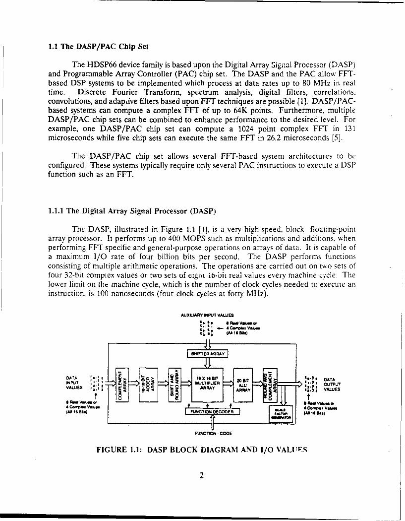
The DASP, illustrated in Figure 1.1 [1], is a very high-speed, block floating-pointarray processor. It performs up to 400 MOPS such as multiplications and additions, whenperforming FFT specific and general-purpose operations on arrays of data. It is capable ofa maximum I/O rate of four billion bits per second. The DASP performs functionsconsisting of multiple arithmetic operations. The operations are carried out on two sets offour 32-bit compiex values or two sets of eight !6-bit real vaiueb every machine cycle. Thelower limit on die machine cycle, which is the number of clock cycles needed to execute aninstruction, is 100 nanoseconds (four clock cycles at forty MHz).
AUXILIARY INPUT VALUES
SHIFTER ARRAY
DATA 00" a 20IOI O V DAsAINU MLTIPLIER DATAoj~u
ARRAY IF VALUES
tls t ~s~
4CorYlas Vas # # 4 coiipz use or(All 16 B26) C s) is Vaue
FUNCTION - CODE
FIGURE 1.1: DASP BLOCK DIAGRAM AND I/0 VALVUS
2
The values input to the DASP and output from it are 16-bit fixed point numbers,represented in fractional two's complement arithmetic. To preserve an adequate signal-to-noise ratio as intermediate operations are carried out, intermediate values can grow to 20bits. These same values are rounded to 16 bits upon transfer to the output busses. In fixed-point machines scaling is applied to prevent overflow. This must be taken into considerationas there is often an accompanying loss in signal-to-noise ratio.
1.1.2 The Programmable Array Controller (PAC)
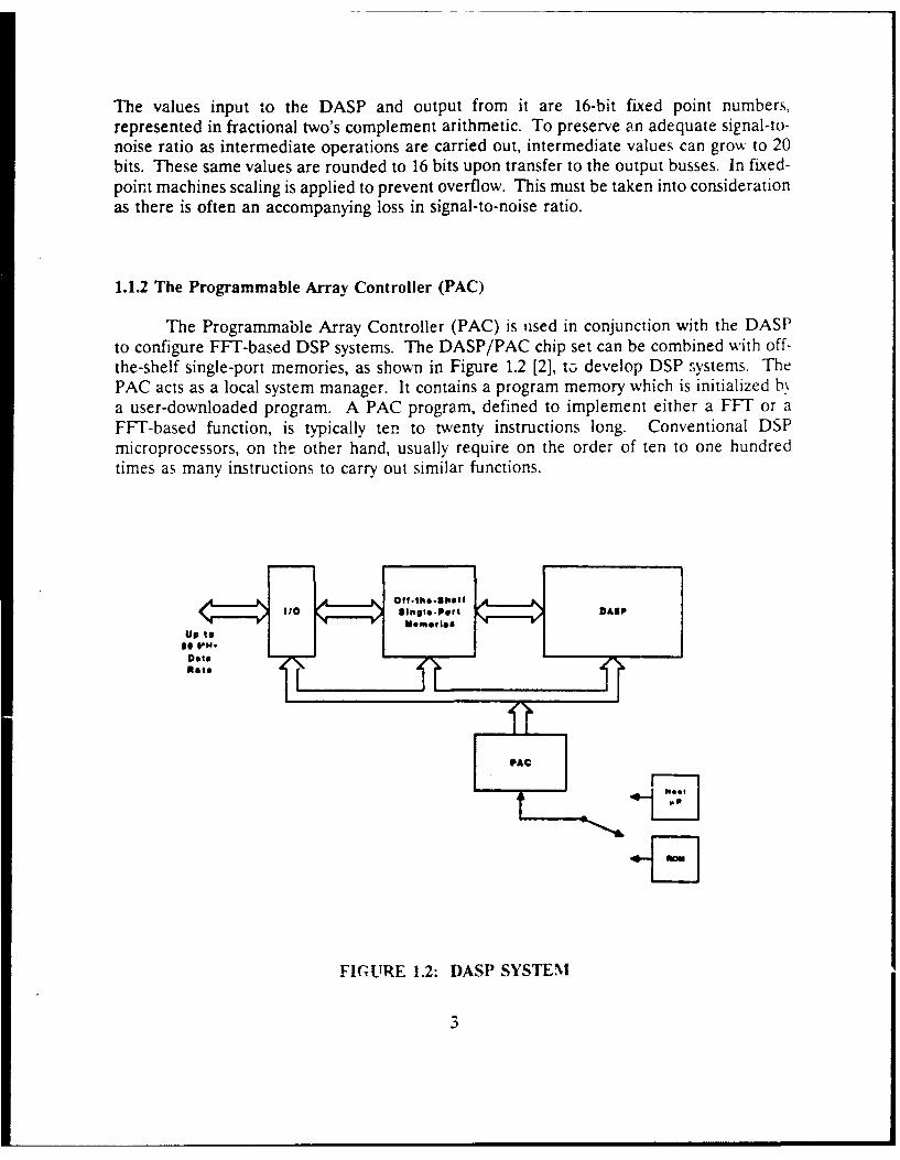
The Programmable Array Controller (PAC) is used in conjunction with the DASPto configure FFT-based DSP systems. The DASP/PAC chip set can be combined with off-the-shelf single-port memories, as shown in Figure 1.2 [2], t3 develop DSP systems. ThePAC acts as a local system manager. It contains a program memory which is initialized b%a user-downloaded program. A PAC program, defined to implement either a FFT or aFFT-based function, is typically ten to twenty instructions long. Conventional DSPmicroprocessors, on the other hand, usually require on the order of ten to one hundredtimes as many instructions to carry out similar functions.
FIGURE 1.2: DASP SYSTEM
=3
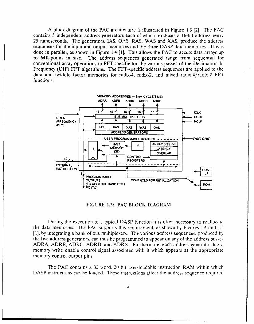
A block diagram of the PAC architecture is illustrated in Figure 1.3 [2]. The PACcontains 5 independent address generators each of which produces a 16-bit address everx25 nanoseconds. The generators, IAS, OAS, RAS, WAS and XAS, produce the addresssequences for the input and output memories and the three DASP data memories. This isdone in parallel, as shown in Figure 1.4 [1]. This allows the PAC to access data arrays upto 64K-points in size. The address sequences generated range from sequential forconventional array operations to FFT-specific for the various passes of the Decimation InFrequency (DIF) FFT algorithms. The FFT-specific address sequences are applied to thedata and twiddle factor memories for radix-4, radix-2, and mixed radix-4/radix-2 FFTfunctions.
(MEMORY ADDRESSES - Tmi4 CYCLE TIME)ADRA ADRB ADRX ADRC ADAD
16 1 16 16 1 4 - ICU(
CLKIN BUS MULTIPLEXERS 4-OICLK(FREQUENCY + + +--HOLK4 m )
ADDRESS GENERATORS
- USER-PROGRAMMABLE CONTROL --.-- - , 4-PAC CHIP
INST ARRAY SIZE N
+ MEMORY *-- LATENCY1 (32) C & OVERLAP
12 = , , CONTROL .___
A1REGISTERS-- --- TEXTERNAL . -- --.--- -- ---INSTRUCTION HOST
/PROGRAMMABLE IOUTPUTS CONTROLS FOR INITIALIZATION t,
(TO CONTROL DASP ETC.)PO (7 )
FIGURE 1.3: PAC BLOCK DIAGRAM
During the execution of a typical DASP function it is often necessary to reallocatethe data memories. The PAC supports this requirement, as shown by Figures 1.4 and 1.5[1], by integrating a bank of bus multiplexers. The various address sequences, produced bthe five address generators, can thus be programmed to appear on any of the address bussesADRA, ADRB, ADRC, ADRD, and ADRX. Furthermore, each address generator has amemory write enable control signal associated with it which appears at the appropriatememory control output pins.
The PAC contains a 32 word, 20 bit user-loadable instruction RAM within whichDASP instructions can be loaded. These instructions affect the address sequcnce required
4

of the address generators, and the programming of the address generators to the desiredaddress buses. The PAC contains several user-loadable control registers which allow severalsystem configurations to be defined. These control registers contain system configurationparameters which are discussed in Section 5.3.2. The PAC is typically initialized and hostedby an additional microprocessor. Alternatively, the PAC can autobootlozd itself from anexternal ROM.
DATA DATAINPUT OUTPUT
A1 0
ADAC
jCOEFFM-DENTS
ADAADSADFLX ADRC AR
7A ORA ,ORPAC
FIGURE 1.4: DUAL MEMORY RECURSIVE SYSTEM WITH I/O BUFFERS
DATA DATAINPUT OUTPUT
DAA
AP C
BUFFERS-MEMORY REALLOCATION
I I I

2.0 SYSTEM ARCHITECTURES
The DASP/PAC chip set allows many FFT-based DSP problems to be solved usinga variety of DSP algorithms and system configurations. The three basic system architecturessupported by the chip set are recursive dual memory, recursive single memory, and cascaded[1]. The possible architectures are not restricted to the configurations herein presented butmay be tailored to the application.
2.1 Recursive Dual Memory System-Core
The recursive architecture executes DSP algorithms on a single DASP/PAC stage bycarrying out multiple passes of the data array through the DASP. The architecture of acore, recursive dual memory system is given in Figure 2.1 [1]. The PAC controls the systemand thus the addressing of the three memories, B, C and X. Each of these memories cancontain N words of complex data. N is the size of the array which is passed through theDASP.
DATA IN DATA OUT
!.!,~ 0 D° °1.3R RRI
COEF'W-
CIENTS
ADRB ADRX ADRC
PAC
FIGURE 2.1: CORE DUAL MEMORY RECURSIVE STAGE
The initiation of any system function involves the input address being programmed toappear on the ADRB bus so that N data samples can be loaded in memory B. The DASPprocessing then commences with the PAC sending an instruction code to the DASP toimplement the desired function. The first PAC instruction passes the data from memory Bto memory C by providing the read address sequence on the ADRB bus and the writeaddress sequence on the ADRC bus. An auxiliary address sequence is programmed on theADRX bus to allow the DASP to read from memory X. The current function programmed
6
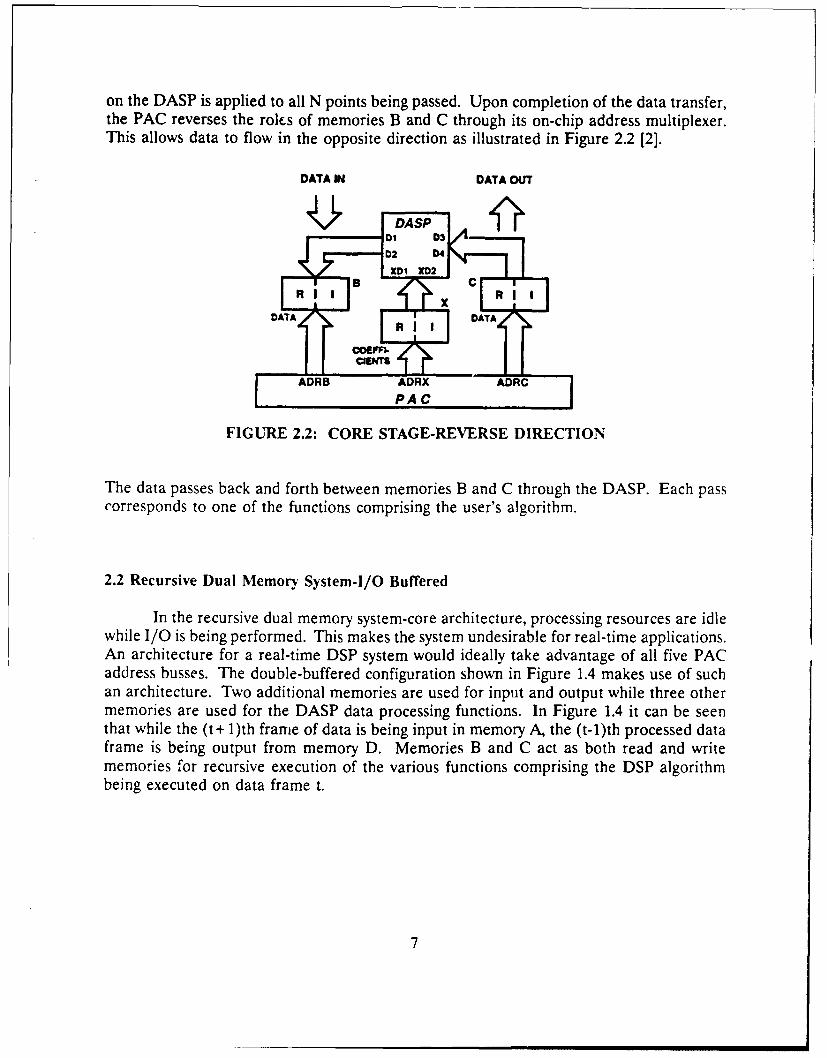
on the DASP is applied to all N points being passed. Upon completion of the data transfer,the PAC reverses the roles of memories B and C through its on-chip address multiplexer.This allows data to flow in the opposite direction as illustrated in Figure 2.2 [2].
DATA IN DATA OUT
Il I
IOi, i
ADRB ADRX ADROPAC
R I I
FIGURE 2.2: CORE STAGE-REVERSE DIRECTION
The data passes back and forth between memories B and C through the DASP. Each passcorresponds to one of the functions comprising the user's algorithm.
2.2 Recursive Dual Memory System-I/O Buffered
In the recursive dual memory system-core architecture, processing resources are idlewhile I/O is being performed. This makes the system undesirable for real-time applications.An architecture for a real-time DSP system would ideally take advantage of all five PACaddress busses. The double-buffered configuration shown in Figure 1.4 makes use of suchan architecture. Two additional memories are used for input and output while three othermemories are used for the DASP data processing functions. In Figure 1.4 it can be seenthat while the (t+ 1)th frame of data is being input in memory A, the (t-1)th processed dataframe is being output from memory D. Memories B and C act as both read and writememories for recursive execution of the various functions comprising the DSP algorithmbeing executed on data frame t.
7
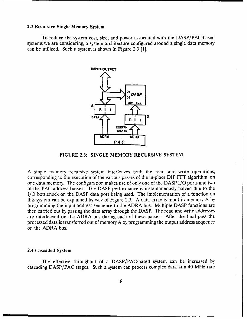
2.3 Recursive Single Memory System
To reduce the system cost, size, and power associated with the DASP/PAC-basedsystems we are considering, a system architecture configured around a single data memorycan be utilized. Such a system is shown in Figure 2.3 [1].
INPUT/OUTPUT
A
ADRA PCADRX
FIGURE 2.3: SINGLE MEMORY RECURSIVE SYSTEM
A single memory recursive system interleaves both the read and write operations,corresponding to the execution of the various passes of the in-place DIF FFT algorithm, onone data memory. The configuration makes use of only one of the DASP I/O ports and twoof the PAC address busses. The DASP performance is instantaneously halved due to theI/O bottleneck on the DASP data port being used. The implementation of a function onthis system can be explained by way of Figure 2.3. A data array is input in memory A byprogramming the input address sequence to the ADRA bus. Multiple DASP functions arethen carried out by passing the data array through the DASP. The read and write addressesare interleaved on the ADRA bus during each of these passes. After the final pass theprocessed data is transferred out of memory A by programming the output address sequenceon the ADRA bus.
2.4 Cascaded System
The effective throughput of a DASP/PAC-based system can be increased bycascading DASP/PAC stages. Such a 3ystem can process complex data at a 40 MHz rate
8
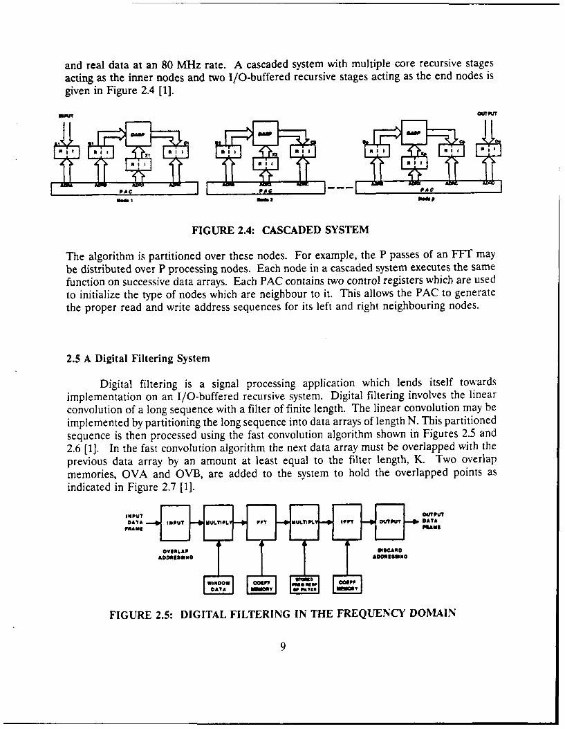
and real data at an 80 MHz rate. A cascaded system with multiple core recursive stagesacting as the inner nodes and two I/O-buffered recursive stages acting as the end nodes isgiven in Figure 2.4 [1].
INO OUTPUT
la014 all
I, Ileal ld 0111O&p
FIGURE 2.4: CASCADED SYSTEM
The algorithm is partitioned over these nodes. For example, the P passes of an FFT maybe distributed over P processing nodes. Each node in a cascaded system executes the samefunction on successive data arrays. Each PAC contains two control registers which are usedto initialize the type of nodes which are neighbour to it. This allows the PAC to generatethe proper read and write address sequences for its left and right neighbouring nodes.
2.5 A Digital Filtering System
Digital filtering is a signal processing application which lends itself towardsimplementation on an I/O-buffered recursive system. Digital filtering involves the linearconvolution of a long sequence with a filter of finite length. The linear convolution may beimplemented by partitioning the long sequence into data arrays of length N. This partitionedsequence is then processed using the fast convolution algorithm shown in Figures 2.5 and2.6 [1]. In the fast convolution algorithm the next data array must be overlapped with theprevious data array by an amount at least equal to the filter length, K. Two overlapmemories, OVA and OVB, are added to the system to hold the overlapped points asindicated in Figure 2.7 [1].
INPUT OWTPUT
DATA INPUT NULTIPL P" MULTIPt of" OWPVT DATAFRIAME I11AW1l
OVIWLIAP NIDSPAO
FIGURE 2.5: DIGITAL FILTERING IN THE FREQUENCY DOMAIN
9
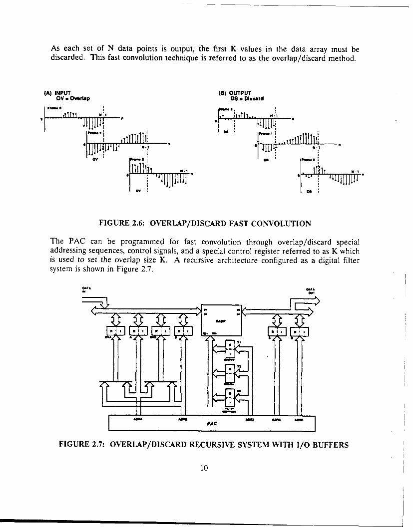
As each set of N data points is output, the first K values in the data array must bediscarded. This fast convolution technique is referred to as the overlap/discard method.
(A) INPUT (B) OUTPUTOV a Overlap DS a Discard
'[ ~~~~ ~ 111 -. .1111! " J liP1 Tl ' . _.,, !111 1
S I'
SN-1
FIGURE 2.6: OVERLAP/DISCARD FAST CONVOLUTION
The PAC can be programmed for fast convolution through overlap/discard specialaddressing sequences, control signals, and a special control register referred to as K whichis used to set the overlap size K. A recursive architecture configured as a digital filtersystem is shown in Figure 2.7.
DATA DATA
PAC
FIGURE 2.7: OVERLAP/DISCARD RECURSIVE SYSTEMI WITH I/O BUFFERS
10
II II II-N
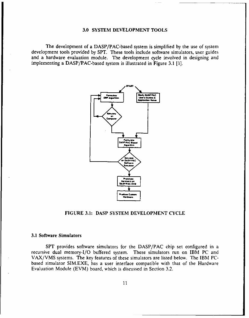
3.0 SYSTEM DEVELOPMENT TOOLS
The development of a DASP/PAC-based system is simplified by the use of systemdevelopment tools provided by SPT. These tools include software simulators, user guidesand a hardware evaluation module. The development cycle involved in designing andimplementing a DASP/PAC-based system is illustrated in Figure 3.1 [1].
an~ DASFIPA
SPIPAC EVM
FIGURE 3.1: DASP SYSTEM DEVELOPMENT CYCLE
3.1 Software Simulators
SPT provides software simulators for the DASP/PAC chip set Configured in a
recursive dual memory-I/O buffered system. These simulators run on IBM PC andVAX/VMS systems. The key features of these simulators are listed below. The IBM PC-based simulator SIM.EXE, has a user interface compatible with that of the HardwareEvaluation Module (EVM) board, which is discussed in Section 3.2.
11
The VAX/VMS-based simulator is a stand-alone simulation tool. It can also beintegrated into a larger simulation by being called as a subroutine. The VAX/VMS-basedsimulator was not used in this study.
The key features of the IBM PC based simulator include [2]:
i) A menu-driven user interface,ii) A capability to generate data arrays consisting of two sinusoids,iii) The DSP algorithm being defined through graphical models of the PAC
instruction memory and control registers,iv) Algorithm execution being carried out on a model of the DASP,v) Graphical displays for data arrays, andvi) I/O file capability for data arrays and programs.
The key features of the VAX/VMS based simulator include [2]:
i) Coding in "C" language to allow linking with user defined system simulations,ii) Algorithm execution being carried out on an integrated model of the
DASP/PAC chip set, andiii) Corresponding floating point computations being available for examination of
errors due to scaling and round-off.
3.2 Hardware Evaluation Module (EVM)
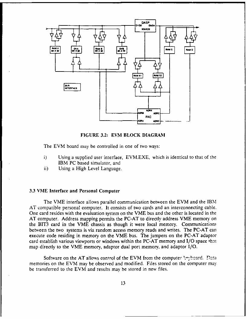
The EVM board is a DASP/1PAC-based digital signal processing system implementedon a Eurocard SU-9 standard size board for VME bus systems. FFT-based signal processingalgorithms can be implemented on the EVM to process data at rates currently available inVME bus products. The EVM allows the designer to prototype and evaluate a proposedDSP system. A block diagram of the EVM is given in Figure 3.2 [1]. A more detaileddescription of the EVM is found in Section 4.0.
12
PAM ~~~ ~ A A V=nPMC PM
FIGURE 3.2: E,, BLOCK DIAGRAM
The EVM board may be controlled in one of two ways:
i) Using a supplied user interface, EVM.EXE, which is identical to that of theIBM PC based simulator, and
ii) Using a High Level Language.
3.3 VME Interface and Personal Computer
The VME interface allows parallel communication between the EVM and the IBMAT compatible personal computer. It consists of two cards and an interconnecting cable.One card resides with the evaluation system on the VME bus and the other is located in theAT computer. Address mapping permits the PC-AT to directly address VME memory onthe BIT3 card in the VME chassis as though it were local memory. Communicationsbetween the two systems is via random access memory reads and writes. The PC-AT canexecute code residing in memory on the VME bus. The jumpers on the PC-AT adaptorcard establish various viewports or windows within the PC-AT memory and I/O space thatmap directly to the VME memory, adaptor dual port memory, and adaptor I/O.
Software on the AT allows control of the EVM from the computer %!-,tcard. D.!amemories on the EVM may be observed and modified. Files stored on the computer maybe transferred to the EVM and results may be stored in new files.
13
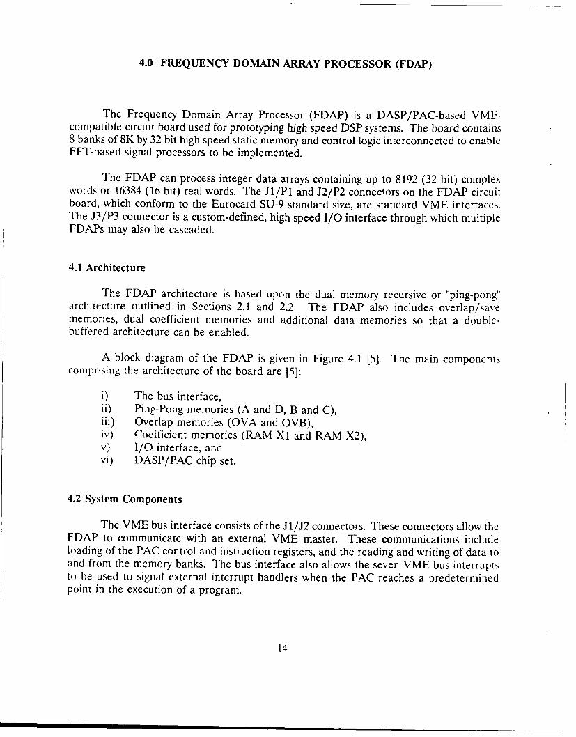
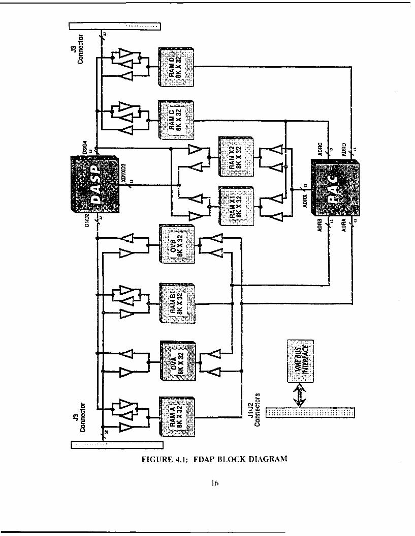
4.0 FREQUENCY DOMAIN ARRAY PROCESSOR (FDAP)
The Frequency Domain Array Processor (FDAP) is a DASP/PAC-based VME-compatible circuit board used for prototyping high speed DSP systems. The board contains8 banks of 8K by 32 bit high speed static memory and control logic interconnected to enableFFT-based signal processors to be implemented.
The FDAP can process integer data arrays containing up to 8192 (32 bit) complexwords or 16384 (16 bit) real words. The J1/P1 and J2/P2 connectors on the FDAP circuitboard, which conform to the Eurocard SU-9 standard size, are standard VME interfaces.The J3/P3 connector is a custom-defined, high speed I/O interface through which multipleFDAPs may also be cascaded.
4.1 Architecture
The FDAP architecture is based upon the dual memory recursive or "ping-pong"architecture outlined in Sections 2.1 and 2.2. The FDAP also includes overlap/savememories, dual coefficient memories and additional data memories so that a double-buffered architecture can be enabled.
A block diagram of the FDAP is given in Figure 4.1 [5]. The main componentscomprising the architecture of the board are [5]:
i) The bus interface,ii) Ping-Pong memories (A and D, B and C),iii) Overlap memories (OVA and OVB),iv) Coefficient memories (RAM X1 and RAM X2),v) I/O interface, andvi) DASP/PAC chip set.
4.2 System Components
The VME bus interface consists of the J1/J2 connectors. These connectors allow theFDAP to communicate with an external VME master. These communications includeloading of the PAC control and instruction registers, and the reading and writing of data toand from the memory banks. The bus interface also allows the seven VME bus interruptsto be used to signal external interrupt handlers when the PAC reaches a predeterminedpoint in the execution of a program.
14
The FDAP's ping-pong memory consists of four banks of 8Kx32 bit memory, A, B,C and D. It is referred to as ping-pong memory because data is passed recursively back andforth between pairs of memory banks. The PAC's ADRA, ADRB, ADRC, and ADRDaddress busses are used to address the four banks as shown in Figure 4.1. Banks A and Bmay be programmed to be either input memories or DASP read/write memories. If theyare read/write memories their data busses are subsequently gated onto the DASP DI andD2 data busses. Similarly, banks C and D may be programmed to be either outputmemories or DASP read/write memories.
When a fast convolution filtering algorithm using the overlap/discard technique isto be implemented, two banks of 8Kx32_ bit memory are used to hold the overlappedportions of the input data. These two memory banks, OVA and OVB, support overlaps ofup to 2K-points.
Coefficient memories X1 and X2, also referred to as auxiliary memories, are each8Kx32 bit high-speed static memory banks. The DASP's auxiliary data bus may be routedto either auxiliary memory and the remaining memory may be concurrently written to fromthe DASP's D3/D4 bus. The two most significant bits of the PAC programmable output,which are discussed in Section 5.4, control the routing to the coefficient memories. Bit 6determines the routing of the DASP auxiliary data bus while bit 7 enables the memoryrouted to the DASP D3/D4 bus to be written to.
The high-speed I/O interface is implemented through a 96 pin J3 connector on theFDAP. The interface consists of a 32 bit input bus, 32 bit output bus and control and statussignals. Both busses are 32 bit complex. The input bus may be -ated directly into eithermemory A or B or one of the overlap memories. The output bus may originate from eithermemory C or D.
15
cq
C4cl)
'Mao
clC404Xcl)
...........cr. c*
C-4x C.)
cc
co
co
co .,k :
uj
P. C-4
co
10C'i r
Cc
FIGURE 4.1: FDAP BLOCK DIAGRAM
16
5.0 PROGRAMMING THE FDAP
The FDAP memory banks and control and status registers are memory mapped tooccupy 64K of VME memory space. The processing memories occupy the upper 32K bytesof FDAP address space. At any given moment, one of the eight 32K byte processingmemories can be bank selected to occupy this space.
5.1 Memory Map
The VME memory map for the FDAP is illustrated in Figure 5.1 [5]. The controland status registers may be jumpered on the BIT3 card (which is located in the VMEchassis) to occupy any one of the 16 different locations indicated. In our exampleControl/Status Location# I is made use of and is expanded on in Figure 5.2 [5]. The FDAPbase address must be set to a 64K byte boundary corresponding to an unused block in thePC-AT. The remote bus RAM jumper setting permits the PC-AT to read and write to theBIT3 memory card in the PC and thus the BIT3 VME adaptor card and processor cardresiding in the VME chassis. The HI and LO RAM jumpers (on the BIT3 card in the VMEchassis) select the address range that the PC-AT will reference in its address space whenit wants to read or write to memory in the VME bus. The remote RAM LO jumper setsthe starting PC-AT address and the remote RAM HI selects the ending address. For thisboard the start address is DOOOO hex and the end address is DEEEF hex. Data istransferred in 16 bit blocks to the FDAP as each FDAP memory location contains 16 bits.
17
base + FFFE II Pnes eea II II B Swmha i
base + 8000 I I
base + 7FFE I II IReserv I
base + 4000 I
base + 3FFE I CorfVStas Loction #16 Ibase+3C00 I I
base + 3BFE I CoatoYStatus Location#15 Ibase + 3800 I I
base + 37FE I II II I
base + oCo I
base + OBFE I CaLocdon#3 Ibase +o8o I I
base + 07FE CortsuLoction2 Ibase + 0400
base + 03FE I CoY StjsLocai #1 Ibase +0000 I
FIGURE 5.1: MEMORY MAP
5.2 Control and Status Registers
5.2.1 Memory Map
The memory map for the FDAP's control and 'tatus registers. Location# I isillustrated in Figure 5.2. Most of the registers can be both read from and written to. TheChase address for the Control/Status location is sct via jumpers on the BIT3 card in theVME chassis. The PAC control registers are expanded on in Section 5.3 and Figure 5.3 [5].The control and status registers occupy five words starting at memory location Cbase + 200Hex. These registers allow the user to set up interrupts, PAC execution modes, map in orout of various processing memory banks, and set up methods for handling scale factors forblock floating point. For our board Chase is set to DOOGO hex.
18
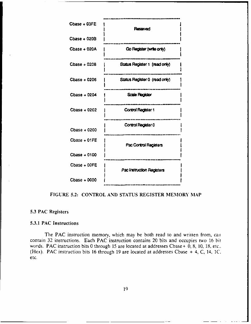
Cbase+ 03FE I II Reserved II I
Cbase + 020B I I
Cbase+ 020A I GRegister vt orM II I
Cbase +0208 I Status Register 1 (read oly) II I
Cbase + 0206 I Status Regier 0 (read only) I1 I
Cbase + 0204 I Scaie Rsaer II I
Cbase +0202 I Cortrol Register1 II I
I Cont:o Register0 ICbase + 0200 I I
Cbase + 01FE I II Pac Cortml Regisers I
Cbase+0100 I I
Cbase + OOFE I II Pac InsMcion Rgiters II I
Cbase + 0000 I I
FIGURE 5.2: CONTROL AND STATUS REGISTER MEMORY MAP
5.3 PAC Registers
5.3.1 PAC Instructions
The PAC instruction memory, which may be both read to and written from, cancontain 32 instructions. Each PAC instruction contains 20 bits and occupies two 16 bitwords. PAC instruction bits 0 through 15 are located at addresses Cbase+ 0, 8, 10, 18, etc..(Hex). PAC instruction bits 16 through 19 are located at addresses Cbase + 4, C, 14, IC,etc.
19
5.3.2 PAC Control Registers
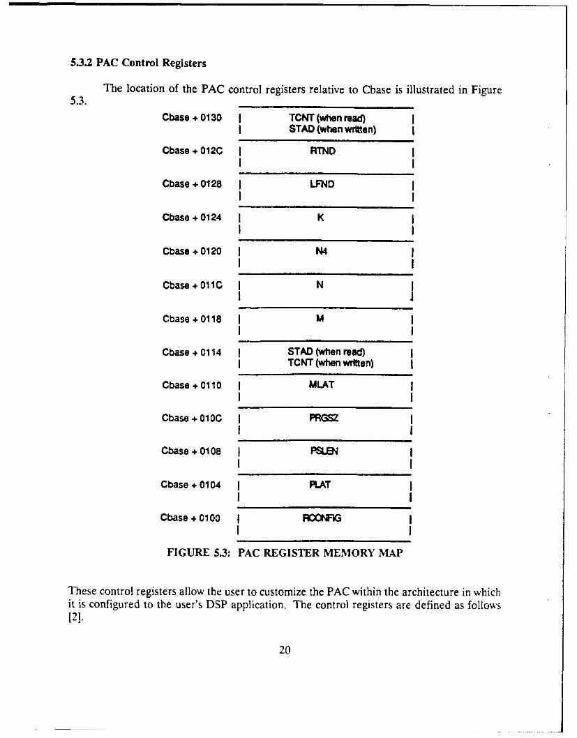
The location of the PAC control registers relative to Cbase is illustrated in Figure5.3.
Cbase + 0130 I TCNT (whenread) II STAD (when wrtten) I
Cbase + 012C I RTND II I
Cbase + 0128 I LFND II I
Cbase +0124 j KI I
Cbase + 0120 I N4 II I
Cbase + 011C I NI I
Cbase + 0118 I M II I
Cbase + 0114 I STAD (when read) II TCNT (when written) I
Cbase + 0110 I MLAT II I
Cbase + 010C I PRGSZ II I
Cbase + 0108 I PSLEN II I
Cbase + 0104 I LAT II I
Cbase + 0100 I MFIG II I
FIGURE 5.3: PAC REGISTER MEMORY MAP
These control registers allow the user to customize the PAC within the architecture in whichit is configured to the user's DSP application. The control registers are defined as follows[2].
20
RCONFIG:This iegister informs the PAC about the system configuration and the type of algorithm tobe executed. This in turn defines the mode of operation for the PAC. The modes ofoperation include radix-2, radix-4, and mixed-mode radix FFTs, recursive, auto-start, digit-reversed write address and filter.
PLAT:This register defines the processor latency in machine clock cycles introduced by the pipelinebetween the DASP input and output. PLAT must be set to four for proper operation of theDASP as configured in the FDAP architecture.
PSLEN:This register contains the user-specified pause length, in machine clock cycles, required atthe completion of a pass. This register is used when the PAC is operating in the auto-restart mode. The Auto-Restart bit is in the RCONFIG register. This bit configures thePAC to enter the pause mode at the completion of a pass before executing the nextinstruction.
PRGSZ:This register defines the size of the program which has been loaded into PAC internalinstruction memory. The upper limit on PRGSZ is 32.
MLAT:This register defines the memory latency which is present in the data and address paths ofthe read, write, and auxiliary data memories.
STAD:This register defines the starting address, or page offset required when addressing N pointswithin a frame of data.
TCNT:This register is for test purposes.
M:This register contains the exponent of the radix used in the FFT which satisfies thedefinition for data array size N=(radix)**M.
N:This register defines the size of the data array and is defined as N=(radix)**M.
M4:This register is used to generate the appropriate address sequencing for the mixed-radix FFTmode. It determines the half array size and is defined as (M-1)/2.
21
K:This register defines the overlap size required for the fast convolution overlap/discarddigital filtering algorithm.
LFND and RTND:These registers are used for defining the left and right neighbouring nodes if multipleFDAPs are used in a cascaded system.
5.4 Instruction Format
Each PAC instruction consists of 20 bits partitioned into five fields as shown inFigure 5.4 [2]. The fields are node type, mixed-radix mode, auxiliary address shift factor,bus switch code, and programmable output. The node type field is discussed in Section5.4.1. The mixed-radix mode bit is used when a mixed-mode (combination radix-2, radix-4)FFT is to be implemented. The array size for a mixed-mode FFT is an odd power of 2.The mixed-radix mode bit allows the same sine/cosine memories to be used for the variouspasses in the mixed-mode FFT. The auxiliary shift factor defines the number of bitpositions the auxiliary address is to be shifted to the left for one mode with respect to theother. The bus switch code defines how the input, output, read and write address generatorsare routed to address ports ADRA, ADRB, ADRC and ADRD. The programmable outputis discussed in Section 5.4.2.
XSH1F ,IMOD
PO BSC ND
!111111 lIII IIIIsom don sf 1114 Sm
FIGURE 5.4: PAC INSTRUCTION FORMAT
5.4.1 Node Type Field
The 5-bit node type field in the PAC instruction specifies the type of addresssequence, sequential or FFT specific, required of the read, write and auxiliary addressgenerators. Table 5.1 [2] lists all of the node types supported, their mnemonics and theircorresponding Hex codes for the 5 bit field.
22
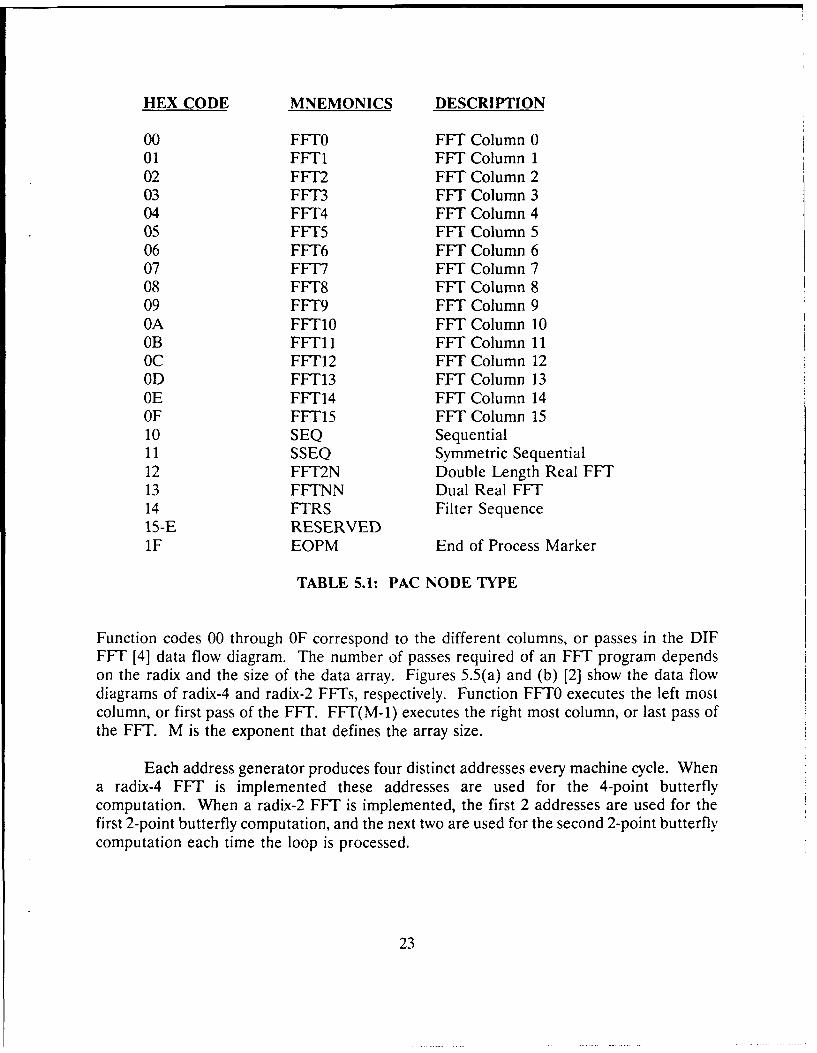
HEX CODE MNEMONICS DESCRIPTION
00 FFTO FFT Column 001 FFT1 FFT Column 102 FFT2 FFT Column 203 FFT3 FFT Column 304 FFTF4 FFT Column 405 FFT5 FFT Column 506 FFT6 FFT Column 607 FF17 FFT Column 708 FFT8 FFT Column 809 FFT9 FFT Column 9OA FFT1O FFT Column 10OB FFT11 FFT Column 11OC FFT12 FFT Column 12OD FFT13 FFT Column 13OE FFT14 FFT Column 14OF FFT15 FFT Column 1510 SEQ Sequential11 SSEQ Symmetric Sequential12 FFT2N Double Length Real FFT13 FFTNN Dual Real FFT14 FTRS Filter Sequence15-E RESERVED1F EOPM End of Process Marker
TABLE 5.1: PAC NODE TYPE
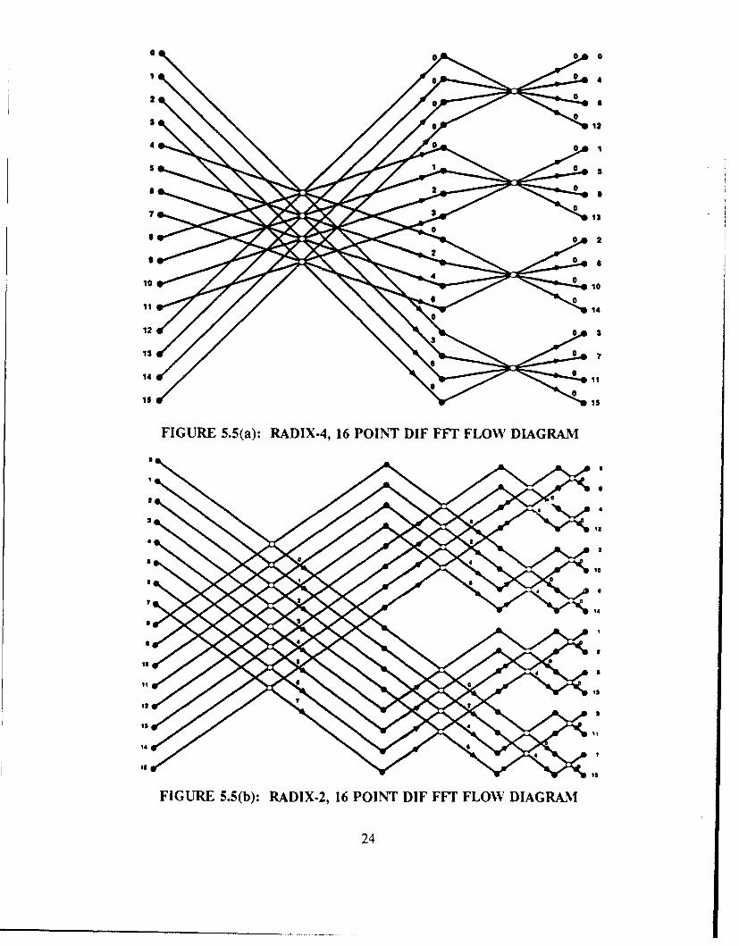
Function codes 00 through OF correspond to the different columns, or passes in the DIFFFT [4] data flow diagram. The number of passes required of an FFT program dependson the radix and the size of the data array. Figures 5.5(a) and (b) [2] show the data flowdiagrams of radix-4 and radix-2 FFTs, respectively. Function FFTO executes the left mostcolumn, or first pass of the FFT. FFT(M-1) executes the right most column, or last pass ofthe FFT. M is the exponent that defines the array size.
Each address generator produces four distinct addresses every machine cycle. Whena radix-4 FFT is implemented these addresses are used for the 4-point butterflycomputation. When a radix-2 FFT is implemented, the first 2 addresses are used for thefirst 2-point butterfly computation, and the next two are used for the second 2-point butterflycomputation each time the loop is processed.
23
0 0
2 12
a0
1 12
122
14 14
1s Is
FIGURE 5.5(a): RADIX-4, 16 POINT DIF FF1' FLOW DIAGRAM
4I
14
13
FIGURE 5.5(b): RADIX-2, 16 POINT DIF FF1' FLOW DIAGRAM
24
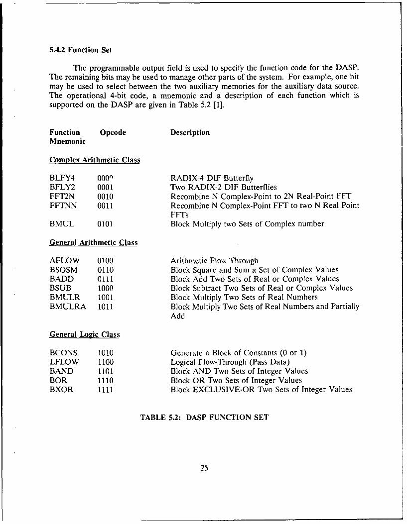
5.4.2 Function Set
The programmable output field is used to specify the function code for the DASP.The remaining bits may be used to manage other parts of the system. For example, one bitmay be used to select between the two auxiliary memories for the auxiliary data source.The operational 4-bit code, a mnemonic and a description of each function which issupported on the DASP are given in Table 5.2 [1].
Function Opcode Description
Mnemonic
Complex Arithmetic Class
BLFY4 0000 RADIX-4 DIF ButterflyBFLY2 0001 Two RADIX-2 DIF ButterfliesFFT2N 0010 Recombine N Complex-Point to 2N Real-Point FFTFFTNN 0011 Recombine N Complex-Point FFT to two N Real Point
FFTsBMUL 0101 Block Multiply two Sets of Complex number
General Arithmetic Class
AFLOW 0100 Arithmetic Flow ThroughBSQSM 0110 Block Square and Sum a Set of Complex ValuesBADD 0111 Block Add Two Sets of Real or Complex ValuesBSUB 1000 Block Subtract Two Sets of Real or Complex ValuesBMULR 1001 Block Multiply Two Sets of Real NumbersBMULRA 1011 Block Multiply Two Sets of Real Numbers and Partially
Add
General Logic Class
BCONS 1010 Generate a Block of Constants (0 or 1)LFLOW 1100 Logical Flow-Through (Pass Data)BAND 1101 Block AND Two Sets of Integer ValuesBOR 1110 Block OR Two Sets of Integer ValuesBXOR 1111 Block EXCLUSIVE-OR Two Sets of Integer Values
TABLE 5.2: DASP FUNCTION SET
25

6.0 FDAP PROGRAMMING USING A USER INTERFACE
The following sections outline the implementations of two DSP routines on the I/Obuffered recursive system of the FDAP. PAC programs implementing FFTs and pulsecompression routines follow. The examples can be implemented through either the IBMPC-AT simulator or the user interface for the EVM.
The DASP function codes are as defined in the previous sections. These programsare coded to allow the PAC to loop through the algorithm continuously until it reaches theend of the program.
6.1 Radix-4 FFT Program
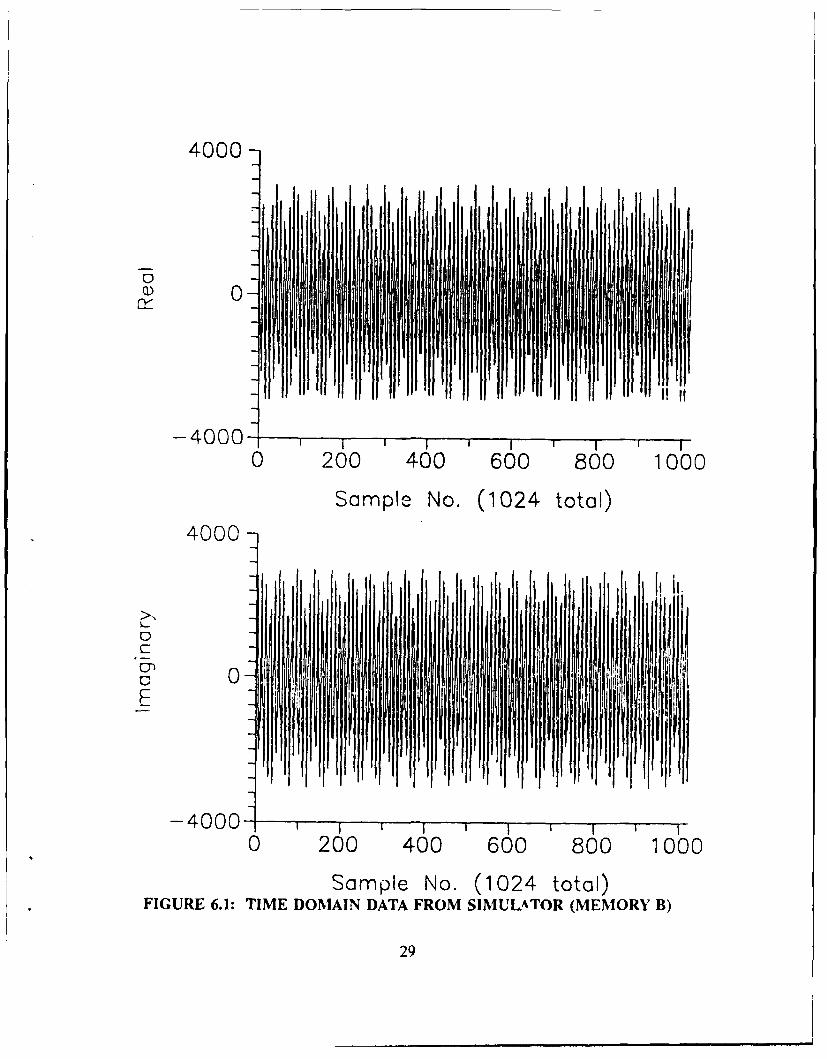
In this example, memories A and/or B can be loaded with 1024 complex words ofdata generated by the simulator program. We have chosen to load memory B. The PACcontrol registers and PAC program memory are set up to do a 5 pass (1024 point), radix-4,complex point FFT on each data set. The program control registers are initialized to handlethe scale factors appropriately. The PAC program is executed, and the results in memoriesD and/or C, C in our case, are plotted.
The simulator generates data according to the simple time domain functionformulated below [51:
0A F' AliF1i A2 2F2i 1X-22 0 e +10 Me ' N J(6.1)
where:
N = the number of samples,i = 0..N- 1,
Al = the amplitude of the first tone (dB),F1 = the frequency bin of the first tone,A2 = the amplitude of the second tone (dB),F2 = the frequency bin of the second tone, andQ = the number of bits (of a tone of amplitude of 0 dB).
26
The following parameters are used in our example for memory B:
N = 1024Al = 0dBFl = 100A2 = -6 dBF2 = 800Q = 12.
A Harris-Blackman window is loaded into Auxiliary Memory X2 via the user interface.Likewise, the twiddle factors for the FFT are loaded into Auxiliary Memory X1. The PACcontrol registers need to be initialized as follows to perform a 1024 complex point,windowed radix-4 FFT:
RCONFIG = 5800HPLAT = 4HPSLEN = 0PRGSZ = 10HMLAT = OOOAHSTAD = 0M =5N =400HM4 = 0 (don't care)K = 0 (don't care) .
The following instruction codes are loaded into the PAC internal instruction memory.
INSTRUCTION # INSTRUCTION DESCRIPTION0 45010 BMUL; Coefficient Mem.; BSC=0; SEQ1 00100 BFLY4; Twiddle Mem.; BSC= 1; FFTO2 00001 BFLY4; Twiddle Mem.; BSC=0; FFT13 00102 BFLV4; Twiddle Mem.; BSC= 1; FFT24 00003 BFLY4; Twiddle Mem.; BSC=0; FFT35 00104 BFLY4; Twiddle Mem.; BSC= 1; FFI46 04010 AFLOW; BSC=0; SEQ7 0401F BSC=0; EOPM8 45310 BMUL; Coefficient Mem.; BSC=3; SEQ9 00400 BFLY4; Twiddle Mem.; BSC=4; FFTOA 00301 BFLY4; Twiddle Mem.; BSC=3; FFT1B 00402 BFLY4; Twiddle Mem.; BSC=4; FFT2C 00403 BFLY4; Twiddle Mem.; BSC=3; FFT3D 00404 BFLY4; Twiddle Mem.; BSC=4; FFT4E 04310 AFLOW; BSC=4; SEQF 0431F BSC=4; EOPM
27
A window operation is first performed on the data array contained in memory B by way ofinstruction 0 (programmable output bit 6 is set to select the coefficient memory).Instructions 1 through 5 subsequently execute the 5 passes of the DIF FFT. Upon thecompletion of instruction 5 the processed data array is stored in memory B. This isspecified by the BSC field of the instruction. The FDAP system is designed to output datathrough either memory C or memory D. Instruction 6 thus executes a flow through pass totransfer the data array in memory B to memory C. Instruction 7 then executes an End ofProcess Marker. This instruction executes what is referred to as a pseudo-pass andsynchronizes the input and output operations on memories A and D with the end of theFFT algorithm. The EOPM instruction causes the processor to initialize an interrupt signalfor one machine cycle. The DASP then performs its housecleaning before a new processis started. Instructions 8 through F execute another FFT. This time data memories A andD are made use of for the FFT.
The time domain data from the simulator which is loaded into Memory B isillustrated in Figure 6.1. The twiddle factors for the FFT, which are loaded into AuxiliaryMemory X1, are given in Figure 6.2. The Harris-Blackman window, which is loaded intoAuxiliary Memory X2, is shown in Figure 6.3. Finally, the FFT of the input data, which isobtained from Memory C, is given in Figure 6.4.
28
4000-
Q) 0
-40000 200 400 600 800 1000
Sample No. (1024 total)
4000
0f. I
0 200 400 600 800 1000
Sample Na. (1024 total)FIGURE 6.1: TIME DOMAIN DATA FROM SIMULATOR (MEMORY B)
29
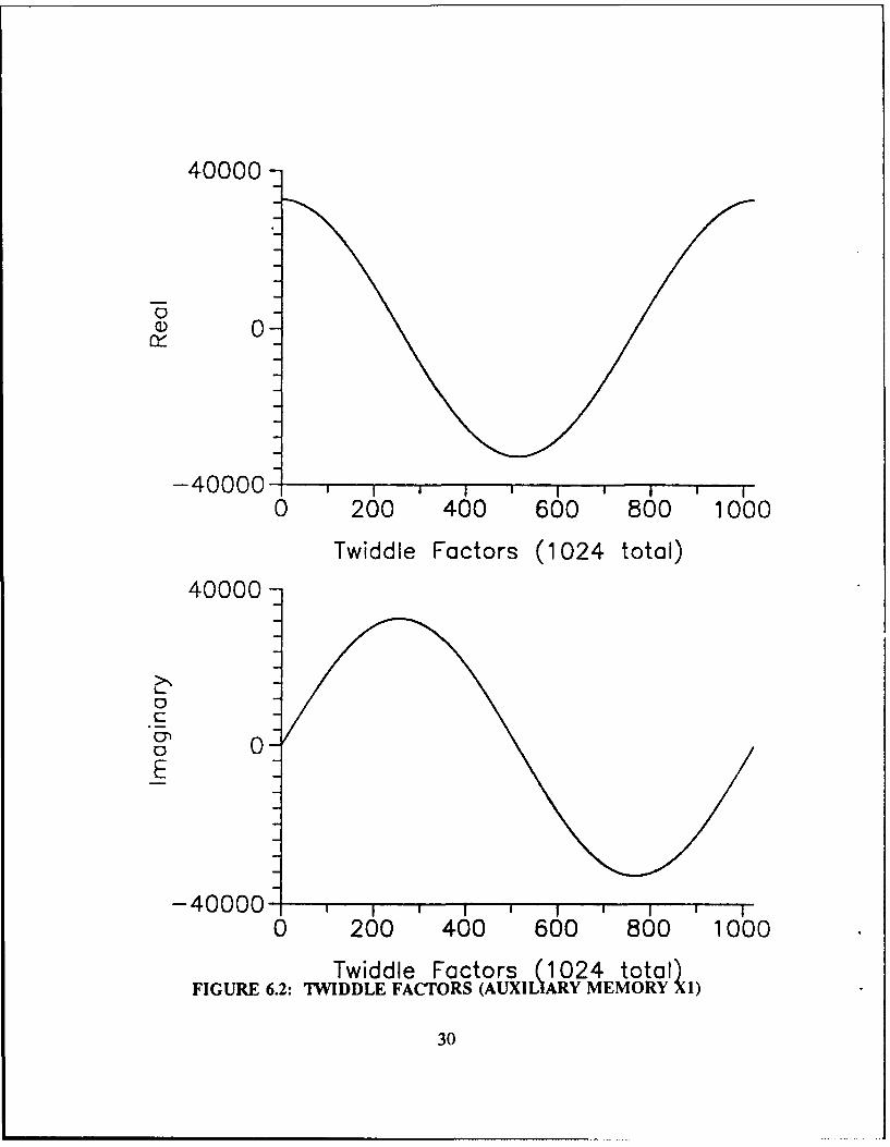
40000-
0-
-40000-
0 200 400 600 800 1000
Twiddle Factors (1024 total)
40000-
0
0 0E
-40000-0 200 400 600 800 1000
Twiddle Factors (1024 total)FIGURE 6.2: TWIDDLE FACTORS (AUXILIARY MEMORY X1)
30
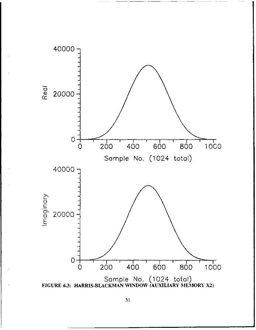
40000-
0m
20000n,"
01-
0 200 400 600 800 1000
Sample No. (1024 total)
40000-
L_0-
o 20000E
0 200 400 600 800 1000
Sample No. (1024 total)FIGURE 6.3: HARRIS-BLACKIAN WINDOW (AUXILIARY MEMORY X2)
31
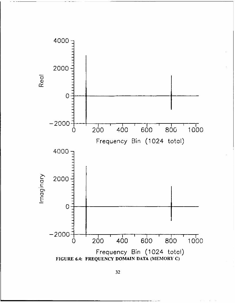
4000-
2000-
00
0 200 400 600 800 1000
Frequency Bin (1024 total)
4000
2000-
0--
-2000--0 200 400 600 800 1000
Frequency Bin (1024 total)FIGURE 6.4: FREQUENCY DOMAIN DATA (MEMORY C)
32
6.2 Pulse Compression Program Using Radix-4 FFTs
6.2.1 Theory of Pulse Compression
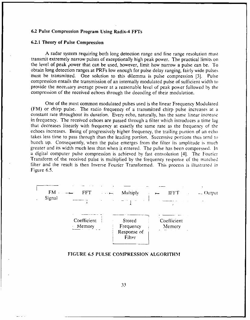
A radar system requiring both long detection range and fine range resolution musttransmit extremely narrow pulses of exceptionally high peak power. The practical limits onthe level of peak power that can be used, however, limit how narrow a pulse can be. Toobtain long detection ranges at PRFs low enough for pulse delay ranging, fairly wide pulsesmust be transmitted. One solution to this dilemma is pulse compression [3]. Pulsecompression entails the transmission of an internally modulated pulse of sufficient width toprovide the necessary average power at a reasonable level of peak power followed by thecompression of the received echoes through the decoding of their modulation.
One of the most common modulated pulses used is the linear Frequency Modulated(FM) or chirp pulse. The radio frequency of a transmitted chirp pulse increases at aconstant rate throughout its duration. Every echo, naturally, has the same linear increasein frequency. The received echoes are passed through a filter which introduces a time lagthat decreases linearly with frequency at exactly the same rate as the frequency of theechoes increases. Being of progressively higher frequency, the trailing portion of an echotakes less time to pass through than the leading portion. Successive portions thus tend tobunch up. Consequently, when the pulse emerges from the filter its amplitude is muchgreater and its width much less than when it entered. The pulse has been compressed. Ina digital computer pulse compression is achieved by fast convolution [4]. The FourierTransform of the received pulse is multiplied by the frequency response of the matchedfilter and the result is then Inverse Fourier Transformed. This process is illustrated inFigure 6.5.
FM - --- FFT -- s Multiply IFFT ) OutputSignal j . .
Coefficient Stored 'CoefficientMemory Frequency Memory
Response of -
Filter
FIGURE 6.5 PULSE COMPRESSION ALGORITHM
33
6.2.2 Pulse Compression On The FDAP Board
All methods of pulse compression are essentially matched filtering schemes in whichthe transmitted pulse is coded and the received pulse is passed through a filter whoseimpulse response is proportional to the conjugate of the time reversed signal.
Since the FDAP software is limited in terms of signal generation, a linear frequencymodulated signal has been generated externally and imported into the FDAP software. Theformulation for the linear FM signal and the matched filter impulse response are as follows:
Linear FM Signal
j2n (fot + kt2/2)s(t) = e (6.2)
Matched Filter Impulse Response
j2t(fo(-t) + k(-t)2/2)s(-t) = e
-j2n (fot - kt 2/2)=e (6.3)
where f. is the initial frequency of the pulse and k is rate of change of the carrier frequency.fo = 0 Hz, k = 400 Hz/second, and t = 0, 1,/N, 2/N, ..., (N-l)/N where N = 1024 for ourexample.
6.2.3 Pailse Compression Program
The PAC cortrol registers need to be initialized as follows to compress a 1024-complex point linear FM pulse. The FFTs used are implemented with a radix-4 algorithm.
RCONFIG = 5800HPRGSZ = BHSTAD = 0M =5N = 400HM4 =0K =0
34
The following program is loaded into the PAC internal instruction memory.
INSTRUCTION # INSTRUCTION DESCRIPTION0 00300 BFLY4; Twiddle Mem.; BSC=3; FFTO1 00401 BFLY4; Twiddle Mem.; BSC=4; FFT12 00302 BFLY4; Twiddle Mem.; BSC=3; FFT23 00403 BFLY4; Twiddle Mem.; BSC=4; FFT34 00304 BFLY4; Twiddle Mem.; BSC=3; FFT45 45410 BMUL; Coefficient Mem.; BSC=4; SEQ6 10300 Complement; BFLY4; BSC=3; FFTO7 00401 BFLY4; Twiddle Mem.; BSC=4; FFT18 00302 BFLY4; Twiddle Mem.; BSC=3; FFT29 00403 BFLY4; Twiddle Mem.; BSC=4; FFT3A 00304 BFLY4; Twiddle Mem.; BSC=3; FFT4
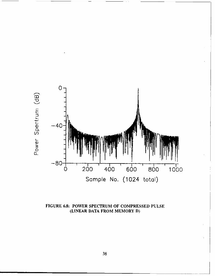
Instructions 0 through 4 execute the 5 columns of the DIF FFT on the FM signal.Instruction 5 multiplies the last FFT with the coefficient memory X2 which contains the FFTof the matched filter. Instruction 6 complements the result of the multiplication so that theinverse Fourier transform may be found using a forward FFT, and at the same timecalculates FFT0. Instruction A performs the last FF1 column and stores the result, thecompressed pulse, in data memory D.
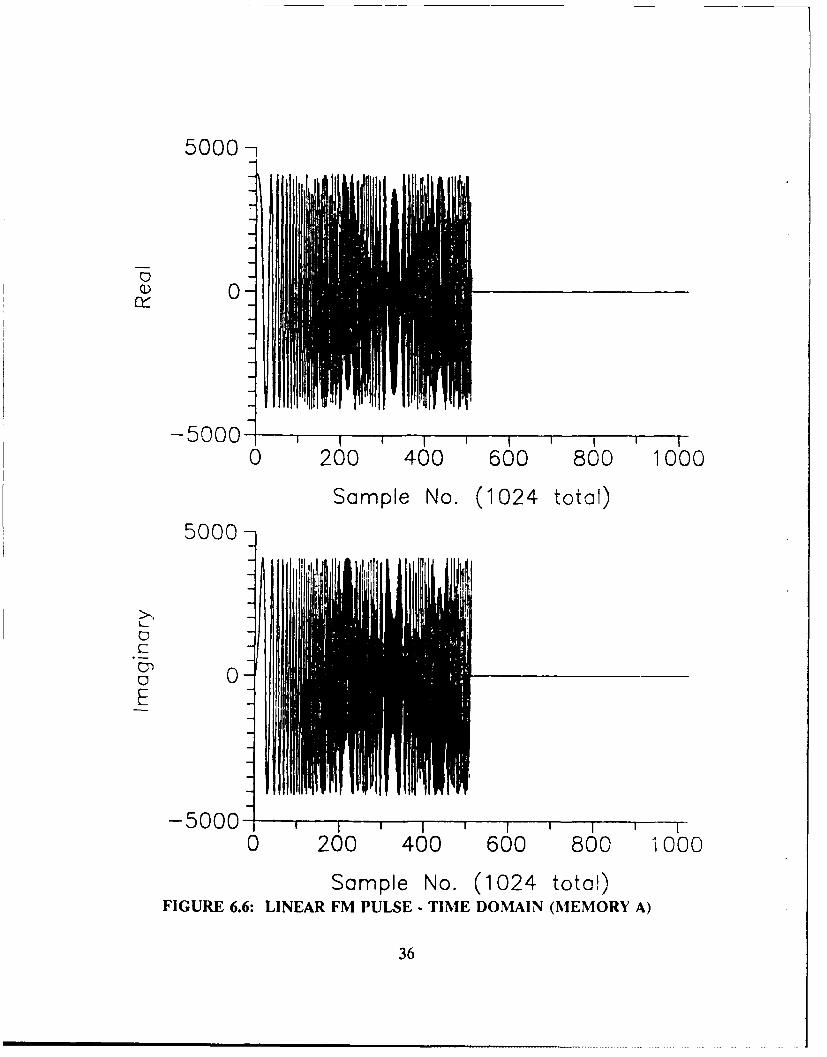
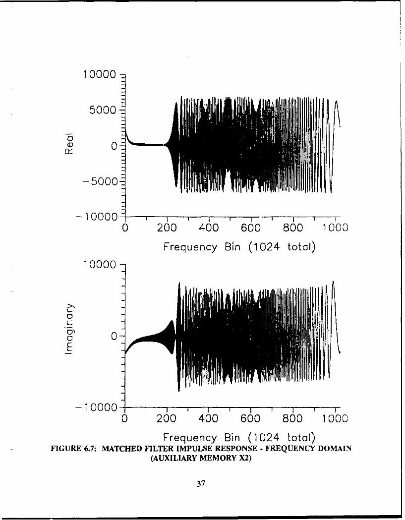
The following plots show the linear FM signal and the subsequent compressed pulse.The linear FM pulse, which is loaded into Memory A, is illustrated in Figure 6.6. Theoriginal pulse consists of 512 points and is zero-padded to 1024 points as required for thefast convolution. The frequency response of the matched filter, which is loaded intoAuxiliary Memory X2, is given in Figure 6.7. This frequency response is computed from a512 point impulse r-sponse which also has been zero-padded to 1024 points. Finally, thepower spectrum of the compressed pulse, which is derived from the complex linear dataoutput from Memory D, is shown in Figure 6.8. The twiddle factors are identical to thosein Figure 6.2 and are stored in Auxiliary Memory X1.
35
5000
0
0 200 400 600 800 1000
Sample No. (1024 total)
5000_
0-E
-5000-0 200 400 600 800 1000
Sample No. (1024 total)FIGURE 6.6: LINEAR FM PULSE - TIME DOMAIN (MEMORY A)
36
10000-
5000-
0
-5000
-10000
0 200 400 600 800 1000
Frequency Bin (1024 total)
10000-
0 00-
E
- 10000
0 200 400 600 800 1000
Frequency Bin (1024 total)FIGURE 6.7: MATCHED FILTER IMPULSE RESPONSE - FREQUENCY DOMAIN
(AUXILIARY MEMORY X2)
37
' 'I I INI W
0
a, -40
0-
0
l-l
-80- .i
0 200 400 600 800 1000
Sample No. (1024 total)
FIGURE 6.8: POWER SPECTRUM OF COMPRESSED PULSE(LINEAR DATA FROM MEMORY D)
38
7.0 FDAP PROGRAMMING USING A HIGH LEVEL LANGUAGE
The FDAP board has the capability to allow a user to program it externally. Toallow direct access/control of the FDAP board, the control and status registers as well asmemory banks have to be initialized. For a detailed explanation of the control and statusbits, refer to the FDAP manual [1]. Appendix 1 contains two programs written in a highlevel language (C) to address the FDAP board. The first program implements a 1024-pointradix-4 complex FFT on the FDAP board. The second program implements a 1024-pointpulse compression routine using radix-4 FFTs. The data used in both of these programs wasthe same data used in Section 6.0 where the FDAP was programmed using the user-interface. Results identical to those presented in Section 6.0 were obtained.
8.0 CONCLUSIONS
The HDSP66 product family from SPT is a new generation of digital signalprocessing products optimized for frequency domain array processing applications. Thefamily offers very high performance, system-based solutions for FFT applications.
The FDAP simulation package and user interface software were used to evaluate theDASP/PAC chip set. The C language was then used to implement FFT and pulsecompression routines to further examine the ease of implementation of typical radar signalprocessing routines which could be integrated into a more sophisticated system.
It was found that the DASP/PAC chip set is a powerful signal processing tool but isnot yet a totally mature product. There are no readily available signal processing routinesfor the FDAP (such as a subroutine library) so that the board must be accessed using thelow-level calls presented in the documentation. The documentation itself is difficult to useand thus the development time is extensive. The C-language programs implemented carriedout their functions to the satisfaction of the users. Follow-up work would entail developinga PC-based SAR processor using the FDAP board as the main computational engine.
39
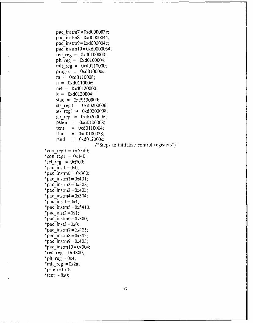
9.0 APPENDIX 1 - FDAP C-LANGUAGE PROGRAM
9.1 1024-Point Radix-4 Complex FF1' Program
#include <stdio.h> /*The following program performs 1024 complex-point FFT5*/main()
unsigned mnt a, b;int i, values, size, ch;int huge *mempointer, *auxpointer, *con_regO, *conregl;mnt huge *scl_reg, *pac -inst], *pac-instm, *pac-instml;int huge *pac -instm-2;mnt huge *rec reg, *mlt reg, *plt_reg, *progsz, *m, *n, *m4;mnt huge *k, 5stad, *fft -node_0, * pac -insi m3, *pacinstm4;int huge *sts regO, *sts regi, *go_reg;mnt huge *pslen, *tcnt, 5 lIfnd, *rtnd;
char *infilename ='c:twd.dat";/ *Step to load the twiddle factor data file to auxiliarymemory*/
char *intype =";FILE *fpl;fp I = fopen(infilename,intype);
con_reg0=OxdO200000; /*Pointer to control register*/*conreg0=Ox53dd; /*Pointer to select auxiliary memory X1 5 /auxpointer =Oxd8000000;
fscanf (fpl, "%X", &values);fscanf (fpl, "%X7', &a);
for (i =1; (i = 1024)&&(!feof(fpl));i + =1){fscanf (fpl, "%X %x", &a, &b);*auxypointer = a;auxypointer + +;* auxpoi nter = bauxpointer+ +;
fclose(fpl);{ /*Steps to download data file to data memory*/char *infilename ="c:fmhex.dat';
char *outfilename = "c:fftfm.dat";
40
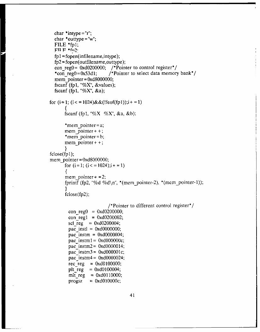
char *intype =r;char *outtype="-"FILE *fpl;F11 F *fn2.fp 1 = fopen(infilename,intype);fp2 = fopen(outfilename,outtype);con regO= OxdO200000; /*Pointer to control register*/*con regO=453dl; /*Pointer to select data memory bank*/mempointer = Oxd8000000;fscanf (fpl, "%X", &values);fscanf (fpl, "%X", &a);
for (i =1; (i < = 1024)&&(!feof(fpl1));i + = 1)
fscanf (fpl, "%X %X", &a, &b);
* mempointer =a;
memypointer+ +;* mempointer = b;
mem_pointer+ +;
fclose(fpl);memjpointer = Oxd8000000;
for (i =1; (i < = 1024);i + = 1)
memypointer+ =2;fprintf (fp2, "%d %d\n", *(mempointer-2), *(memJpointer-1));
fclose(fp2);
/*Pointer to different control register*/con-regO = OxdO200000;con -regi = 0xd0200002;sci-reg = 0xd0200004;pac-instl =OxdOOOOOOO;
pac-instm =OxdOOOOOO4;
pac-instml =OxdOOOOO0c;
pac-instm2= OxdOOOO0l4;pac-instm3= OxdOOOOOlc;pac-instm4 = Oxd0000024;rec-reg =OxdOlOOOOO;
pit_reg =Oxd0lOOOO4;
mlt-reg =Oxd0llOOOO;
progsz =Oxd0lOOO0c;
41
m =OxdOllOOO8;
n = OxdllOOc;m4 =OxdO120000;
k =OxdiOlO0004;
stad =Oxd0l30000;
sts-regO = 0xd0200006;sts-regl = 0xd0200008;goreg = OxdO20000a;pslen =OxdOlOOOO8;
tcnt =Oxd0llOOO4;
lfnd O xd0100028;rtnd =OxdOl2000c;
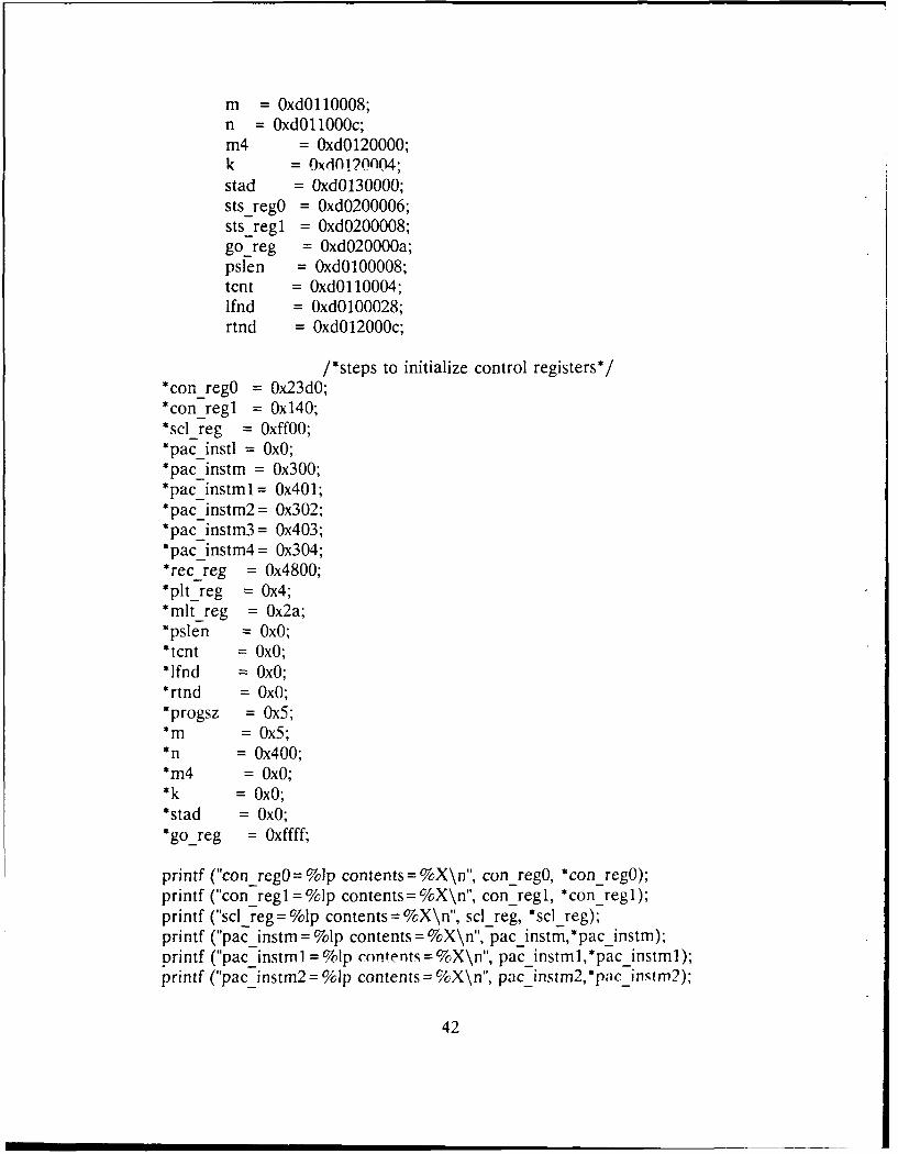
/*steps to initialize control registers*/*c_regO = 0x23d0;* con_regi = 0x140;*scl_reg =OxffOO;*pac instl =OxO;
*pac instm =00300;
*pac instml = 0x401;*pac instm2 = 00302;*pac instm3 = 0x403;*pac instm4 = 00304;*rec_reg = x4800;*pltreg 0xA;*mlt-reg =Ox2a;
*pslen OXO;*tcnt = X0;*lfnd 0x0;*rtnd OxO;* progsz = x5;*M =x5;
* n = x400;*m4 =OxO;
*stad =OxO;
* goreg =Oxffff;
printf ("con rego= %Jp contents = %X\n', con_regO, *con_regO);printf ('con regi = %Ip contents= %X\n", con_regi, *conregl);printf ("sd reg=%Ip contents= %X\n", sci_reg, *scl_reg);printf ("pac -instm =%lp contents = %X\n", pac -instm, *pac_instm);
printf ("pac instm 1 = %lp content,,= %X\n", pac instml ,*pac-instm I);printf ("pac instm2 = %Ip contents = %X\n", pac instm2, *pac-instm?);
42
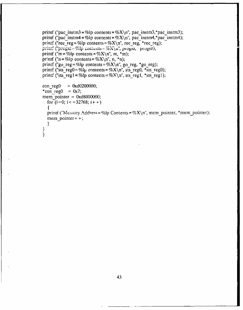
printf ("pac instm3 =%Ip contents =%X\n", pac instrn3, *pac -instm3);printf ("pac -instm4 = %lp contents = %X\n", pac-instm4,*pac-instm4);printf ("rec reg = %p contents =%X\n", rec-reg, * rec-reg);VApi / %I~ ("p;c6gSz -%iP -oii = % ai" pi Ogsz, ,Px Ogsz),printf ("in = %lp contents = %X\n", in, *Sm);pr~ntf ("n = %Ip contents = %X\n", n, *n);printf ("go_reg = %Ip contents = %X\n", go reg, *go_reg);printf ("sts regO = %lp contents = %X\n", sts_regO, *sts_regO);printf ("sts_regi = %Ip contents =%X\n", sts_regi, *sts_regi);
con_regO =OxdO200000;*con regO = x7;mein_pointer = Oxd8000000;
for (i=O; i< =32768; i+ +)Iprintf ('lMvemioAy Address = %Ilp Contents c/%X\n", mempointer, *mempointer):mempointer+ +;
43
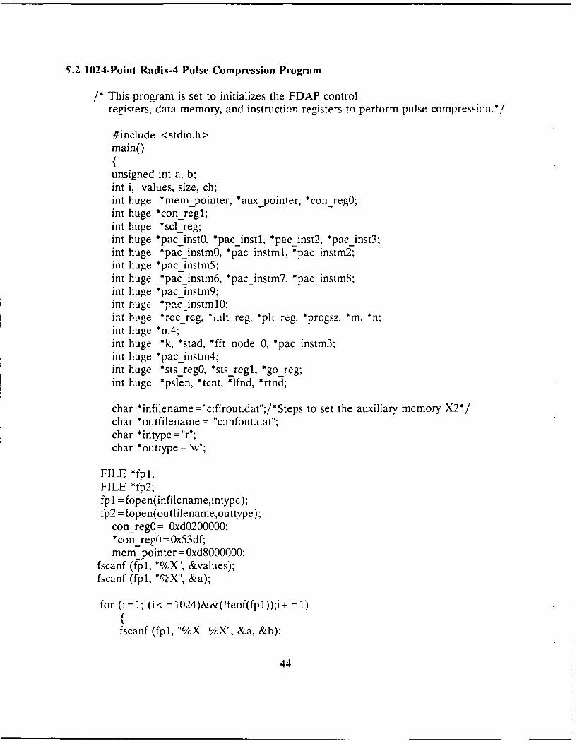
9.2 1024-Point Radix-4 Pulse Compression Program
/* This program is set to initializes the FDAP control
reeiqters, data memory, and instruction registers to perform pulse compression.*/
#include <stdio.h>main()
unsigned mnt a, b;mnt i, values, size, ch;mnt huge *mempointer, *auxpointer, *con-regO;mnt huge scon_regi;mnt huge * sclreg;mnt huge spac -instO, *pac_insti, *pac inst2, *pac_inst3;int huge *pac-instmO, *pacinstml, *pacinstm2;int huge *pac -instm5;mnt huge *pac-instm6, *pacinstm7, *pac_instm8;mnt huge *pac -instm9;int huge *pac _ instmlO;m .t hug.e *rec-reg, *,alt_reg, *plt rcg, *progsz, *m, *n;mnt huge * m4;mnt huge *k, *stad, *fft -nodeO, *pac-instm3:mnt huge *pac -instm4;int huge *sts-regO, *sts_regi, *goreg;mnt huge *pslen, *tcnt, *lfnd, *rtnd;
char *infilename = c:firoutdat";/ *Steps to set the auxiliary memory X2*/char * outfilename = "c:mfout.dat';char * intype =r"
char Souttype =";
FILE *fpl;FILE *fp2;fplI =fopen(infilename,intype);fp2 = fopen(outfilename,outtype);
con_regO = OxdO200000;* con regO =Ox53df;mem pointer = Oxd8000000;
fscanf (fpl, "%X", &values);fscanf (fpl, "%XV, &a);
for (i=I1; (i = 1024)&&(!feof(fpl));i + 1)ffscanf (fpl, "%X %X", &a, &b);
44

*memjpointer a;memypointer+ +;* nem-pointer =b;Tnem-roifte-+ +;
fclose(fp 1);memypointer = 0xd8000000;for (i =1; (i < =1024);i + =1)
memypointer + = 2;fprintf (fp2, "%x %x\n", *(mempointer-2),*(mem~yointer- ));
fclose(fp2);
char *infilename...c:tvddat"; /*Steps to set XI*/char *intype ='r';
FILE *fpl;fplI = fopen(infilename,intype);
con_regO =Oxd 0200000;* con_reg0 =Ox53dd;auxpointer = Oxd8000000;
fscanf (fpl, "%X", &values);fscanf (fpl, "%X", &a);
for (i=1; (i< = 1024)&&(!feof(fpl));i± =1)
fsc,-nf (fpl, "%X %x", &a, &b);* auxjpoiniter =a
auxpointer+ +;* auxJpointer =b;
aux~pointer+ +;
fclose(fpl);
char *infilename="c:fmhexdat"!; /*step to load data memory*/char *outfilename = "c:fftfm.dat";char *intype ="r";char *outtype =";FILE *fpl;FILE *fp2;fpl =fopen(infilename,intype);
45

fp2 = fopen(outfilename,outtype):,
con_regO = OxdO200000;sconrego = x53d 1;mempointer = Oxd8000000;
fscanf (fpl, "%X", &values);fscanf (fpl, "%X", &a);
for (i=1; (i< =1024)&&(!feof(fpI));i+ =1)
f
fscanf (fpl, "'%X %7,X", &a, &b);
*memjpointer =a
memypointer+ ±;* mempointer =b;
mempointer+ +;
fclose(fp 1);
mempointer = Oxd 8000000:for (i =1; (i < =1024);i + = 1)
memypointer+ =2;
fprintf (fp2, "%ld %d\n", *(mernjpointer.2). *(mem_pointer-i)),
fclose(fp2); /*Pointer to control registers*/
con-regO = 0xd0200000;con regi = 0xd0200002:sclireg =0xd0200004;pac_inst0= OxdOOOOOOO;pac_instm =OxdOOOOO4;pac-instm I = OxdOOOOOOc;pac_instm2 = OxdOOOOOl14;pac_instm3 = OxdOOOOO 1 c;pac_instm4 = 0xd0000024;pac_instlI= 0xd0000028;pac_instm5 = OxdOOOOO2c;pac_inst2 = 0xd0000032;pac_instm6 = 0xd0000034;pac inst3 = 0xd0000038;
46
pac instm7 = OxdOOOOO3c;pac_instm8 = 0xd0000044;pac_instm9 = OxdOOOOO4c;pac_instmlO0 = 0xd0000054;recreg =OxdOlOOOOO;
pit reg =OxdOlOOOO4;
mit_reg =OxdOllOOOO;
progsz =OxdOlOOOOc;
m =OxdOllOOO8;
n =OxdOllOO0c;
m4 =OxdOl20000;
k = 0xd0120004;stad = (-1'130000;stsregO =0xd0200006;stsregi =0xd0200008;goreg = xd20000,a;psien =OxdOlOOOOS;
tcn-t =Oxd0llOOO4;
Ifnd = xd0100028;rind =OxdO12OO0c;
/*Steps to initialize control registers*/* con_regO = 0x53d0;* con_regi = 0x140;*scl_reg = OxffOO;*pac instO = OxO;*pac instmO =00300;*pac instmlI =0x401I;*pac instm2 = 00302;*pac instm3 = 0x403;* pac instm4 = 00304;*pac instl1 =0xA;*pac instm5 =0Ox54 10;*pac-inst2- = Ox 1;*pac instm6 = 00300;*pac inst3 = OxO;*pac ins tm7 =1. 41ON.
*pac instr-l 8 = 00302;*pac instm9 = Qx4O3;*pac-instmlO = x304;*rec reg = 0x4800;*pltreg =0x4;*mlt_reg =Ox2a;*pslen = OxO;*tcnt =OXO;
47
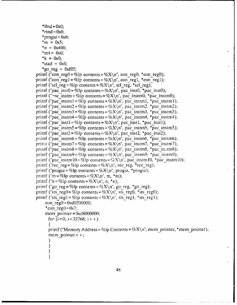
* Ifnd = OxO;* rtnd =OxO;*progsz =Oxb;
" rn 0x5;" n = x400;Sm4 OxO;
*k= OxO;*stad = OxO;* go reg = Oxffff;
printf ('con regO =%lp contents = %X\n", con regO, *con_regO);printf ("con regi = %lp contents= %X\n", con regi, *cocn_regi);printf ("sci reg =%Ip contents = %X\n", sci_reg, *scl_reg);printf ("pac instO= %lp contents = %X\n", pac instO, *pac_instO);printf ("-'ac instm= %lp contents = %X\n", pac instmO, *pac -instmO);printf ("pac_instml = %lp contents= %X\n", pac instml, *pac -instml);printf ("pac_instm2=%lp contents= %X\n", pac_instm2, *pac -instm2);printf ("pac_instm3=%lp contents= %X\n", pac instm3, *pac -instm3);printf ("pac_instm4 =%lp contents = %X\n', pac instm4, *pac -instm4);printf ("pac insti =%lp contents= %X\n", pac insti, *pac_insti);printf ("pac_instm5 =%lp contents = %X\n", pac_instm5, *pacilnstm5);printf ("pac inst2= %lp contents= %X\n", pac inst2, *pac_inst2);p.-intf ("pac-instm6=%Ip contents= %X\n", pac instm6, *pacinstm6);prinir. ("pac_instm7=%lp contents= %X\n". pac_instm7, *pac -instm7);printf ("pac_instm8=%Ip contents= %X\n", pac_instm8, *pac -in-tmg);printf ("pac_instm9=%Icp contents= %X\n", pac_instm9, *pac -instm9);printf ("pac_instmlO=%Ip con tents= %X\n", pac instmlO, *paic-instmlO);printf ("rec_reg=%lp contents= %X\n", rec_reg, *rec_reg);printf ("progsz=%lp contents= %X\n", progsz, *progsz);printf ("m=%Ip contents= %X\n", m, *m);printf ("n=%!p contents=%r/X\n", n, *n);printf ("go reg=%!p contents= %X\n", go reg, *go reg);printf ("sts regO=%lp contents= %X\n", sts_regO, *sts_regO);printf ("sts regi =c/%p contents= r%X\n", sts regi, *sts_regi);
con_regO = OxdO200000;*conreg) = 0x7;mempointer = Oxd18000000;
for (i=O; [<32768; i+ +)fpri ntf ("Memory A ddress = %lip Contents =%X\n", mnem_pointer, *mempointer);memypointer+ +;
48
10.0 REFERENCES
[1) SPT, "Digital Array Signal Processor" User's Guide, Revision 3.0, November 1,1989.
[2] SPT, "Programmable Array Controller" User's Guide, Revision 3.0, November 1,1989.
[3] George W. Stimson, "Introduction to Airborne Radar", Hughes Aircraft Company,El Segundo, California 1983.
[4] Alan V. Oppenheim, "Digital Signal Processing", Prentice-Hall, Inc., EnglewoodCliffs, New Jersey, 1975.
[5] SPT, "Frequency Domain Array Processor", User's Guide, Revision 01/90.
49
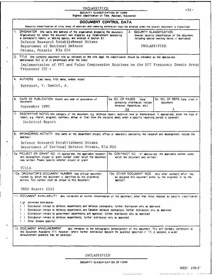
UNCLASSIFIED -51-SECUHITY CLASSIFICATION OF FORM
lhighest classification of Title, Abstract, Keywords)
DOCUMENT CONTROL DATA(Security classification of title, body of abstract and indexing annotation must be entered when the overall document is classfied,
1. ORIGINATOR (the name and address of the organization preparing the document. 2. SECURITY CLASSIFICATIONOrganizations for whom the document was prepared, e.g. Establishment sponsoring (overall security classification of the document.a contractor's report, or tasking agency, are entered in section 8.) including special warning terms if applicable)Defence Research Establishment OttawaDepartment of National Defence UNCLASSIFIED
Ottawa, Ontario KIA 0Z4
3. TITLE (the complete document title as indicated on the title page. Its classification should be indicated by the appropriate
abbreviation (S.C or U) in parentheses after the title.)
Implementation of FFT and Pulse Compression Routines on the SPT Frequency Domain Array
Processor (U) -
4. AUTHORS (Last name, first name, middle initial)
Behroozi, V. Damini, A.
5. DATE OF PUBLICATION (month and year of publication of 6a NO. OF PAGES (total 6b NO. OF REFS (tota' cited indocument) containing information. Include document)
September 1990 Annexes. Appendices, etc.)
58 57. DESCRIPTIVE NOTES ithe ctegory of the document. e.g. technical report, technical note or memorandum. If appropriate, enter the tvpe of
report, e.g. interim, progress, summary, annual or final. Give the inclusive dates when a specific reporting period is covered.)
Technical Report
8. SPONSORING ACTIVITY (the name of the department prolect office or laboratory sponsoring the research and development. Include theaddress.)
Defence Research Establishment Ottawa
Department of National Defence Ottawa, KIA 0Z4
9a PROJECT OR GRANT NO. (if appropriate, the applicable research 9b. CONTRACT NO. iif appropriate, the applicable number underand development orolect or grant number under which the document which the document was wrinenwas written Please specify whether project or grant)
021LA
10a ORIGINATOR'S DOCUMENT NUMBER ithe official document 10b. OTHER DOCUMENT NOS IAny othe, numbers whict maynumber by which the document is identified by the originating be assigned this document either by the originator or by theactivity. This number must be unique to this document. sponsor)
DREO Report 1041
1 1 DOCUMENT AVAILABILITY (any limitations on further dissemination of the document, other than those imposed by securit classiflcation
(x) Unlimited distribution
I I Distribution limited to defence departments and defence contractors; further distribution only as approved
I Distribution limited to defence departments and Canadian defence contractors; further distribution only as approvedI Distribution limited to government departments and agencies; further distribution only as approved
I I Distribution limited to defence departments; further distribution only as approved
Other (please specify)
12 DOCUMENT ANNOUNCEMENT (any limitation to the bibliographic announcement of this document This will normally correspond tothe Document Avallabilty (11) however. where further distribution (beyond the audience specified in 11) is possible, a wide,announcement audience may be selected.)
UNCLASSIFIED
SECURITY CLASSIFICATION OF FORM
DCDO 2/06/8"
-52- UNCLASSIFIED
SECURITY CLASSIFICATION OF FORM
13. ABSTRACT ( a brief and factual summary of the document It may also appear elsewhere in the body of the document itself. It is highlydesirable that the abstract of classified documents be unclassified. Each paragraph of the abstract shall begin with an indication of thesecurity classification of the information in the paragraph (unless the document itself is unclassified) represented as (S), (C), or (U).It is not necessary to include here abstracts in both offical languages unless the text is bilingual).
The Frequency Domain Array Processor (FDAP) is a VME compatible circuit boardbuilt by Signal Processing Technologies (SPT). The FDAP can process integer data arrayscontaining up to 8192 (32 bit) complex words or 16384 (16 bit) real words. It is capable of400 Million Operations Per Second (MOPS) with a maximum Input/Output (I/O) rate offour billion bits per second. It also has a double buffered memory architecture permittingI/O transfers to occur in parallel with data processing. The FDAP can be hosted by anIBM PC/AT-compatible computer using a bus adaptor interface available from BIT3Computer Corp.
The FDAP board is based upon SPT's DASP/PAC chip set. This chip set and thevarious system architectures which can be built around it are reviewed. The FDAP boardand its associated development system are also reviewed. The ease of implementation oftypical radar signal processing functions on the FDAP board are then examined. FastFourier Transform and pulse compression routines are implemented via a supplied userinterface as well as a high level language (C). The results are examined and comments onthe FDAP and its associated system development tools are made.
14. KEYWORDS. DESCRIPTORS or IDENTIFIERS (technically meaningful terms or short phrases that characterize a document and Could behelpful in cataloguing the document. They should be selected so that no security classification is required. Identifiers, such as equipmentmodel designation, trade name, military project code name, geographic location may also be included. if possible keywords Should be selectedfrom a published the:aurus. e.g. Thesaurus of Engineering and Scientific Terms (TEST) and tha' !hesaurus-identified. If it is not Possible toselect indexing terms which are Unclassified, the classification of each should be indicated as with the title.)
Synthetic Aperture Radar
V',i BusFFTPulse Compression
UNCLASSIFIED
SECURITY CLASSIFICATION Or FORM