load-pull analysis for optimizing pa performance
TRANSCRIPT

Load-Pull Analysis for Optimizing PA PerformanceFeaturing Cadence AWR Software
This white paper presents application examples that showcase the load-pull analysis
capabilities in the Cadence® AWR Design Environment® platform, specifically AWR® Microwave
Office® circuit design software, for optimizing power amplifier (PA) performance, including
analysis of simple circuits, matching circuits, and circuit optimization, as well as simulation of
wideband high-efficiency PAs, load-pull measurements for base station PAs, and
synchronized source/load-pull analysis.
Contents
Overview ..............................................................................................................2
Load-Pull Analysis Examples .........................................................................3
Load-Pull Simulation of Wideband High-Efficiency PAs .......................7
Enhanced Load-Pull Measurements for Base station PAs .................14
Synchronized Source/Load-Pull Analysis .............................................. 22
Conclusion ........................................................................................................ 28
WHITE PAPER

OverviewPA performance under small- and large-signal operating conditions is contingent upon the output impedance match (load). As a result, PA designers must determine the ideal output load for system-driven amplifier requirements such as output power at a given saturated power (compression point), efficiency, and/or linearity.
Load-pull simulation is a very simple, yet powerful, concept in which the load or source impedance presented to an active device is swept and its performance is measured. Performance contours are then plotted on a Smith chart, which shows the designer how changing impedances impact the device’s performance (Figure 1).
Figure 1: The load-pull methodology in which the load (or source) impedance presented to the device is swept and measured, then performance contours are plotted on a Smith chart
Load pull has been used for decades in RF circuit design flows, especially for high-power applications such as base station PAs. Advances in data file formats by load-pull measurement system vendors such as Maury Microwave and Focus Microwaves have significantly expanded the usefulness of load-pull characterization. These file formats support a sweep of an independent variable such as input power, DC bias, temperature, or tone spacing (in the case of two-tone load pull), in addition to the swept source or load impedances.
The ability to import and manipulate these load-pull data sets in a circuit simulator greatly simplifies and speeds the design process giving designers a broader design space to explore. This white paper highlights how AWR Microwave Office software enables designers to take full advantage of these load-pull file capabilities in an intuitive manner by offering important load-pull measurement and graphing control features. Today in the industry, many designers are predominantly sweeping input power and, consequently, load-pull features focus on input power sweeps, but it’s important to note that essentially any parameter can be swept and the data manipulated in the design environment.
Load-Pull Analysis for Optimizing PA Performance
2www.cadence.com/go/awr

Load-Pull Analysis ExamplesLoad-pull analysis is one of the key design techniques in amplifier design and is often used for determining an appropriate load. Amplifiers can be designed more efficiently when using load-pull techniques. The following three examples, extracted from a technical seminar presented at the Microwave Workshops & Exhibition in Yokohama, Japan, focus on the load-pull analysis capability within AWR Microwave Office software for analyzing the impact of terminating impedance on device performance, as well as introducing the utilization and optimization of electromagnetic (EM) field analysis using Cadence AWR AXIEM® 3D planar EM analysis to model the impedance matching structure.
Load-Pull Analysis
The AWR software load-pull analysis function sweeps the terminating source and load impedances on the respective input and output sides of the transistors. This enables constant performance contours to be drawn on a Smith chart, thereby showing what load should be connected so as to optimize the transistor performance (Figure 2).
The load-pull analysis not only specifies a particular set of load-pull contours (or overlapping contours), but the software can also calculate and plot a contour for multiple (combined) design criteria, providing the performance characteristics in cases where a matching circuit is connected and enabling designers to execute a more realistic analysis.
Simple Load-Pull Analysis Example
In the example shown in Figure 2, the Smith chart on the top left shows the impedances that were executed by the load-pull analysis and a marker near the center of the red circle corresponds to a mismatch circle with specific voltage standing wave ratio (VSWR) that can be changed by adjusting the VSWR value.
Figure 2: Data sets of simulation results in AWR software enable designers to compare gain compression responses due to varied load impedances
Load-Pull Analysis for Optimizing PA Performance
3www.cadence.com/go/awr

The other graphs in Figure 2 show saved data sets of measured output power versus gain compression (top right), output power versus power-added efficiency (PAE) (bottom left), and input power versus output power (bottom right). The gray plots indicate measured values at all the impedance points and the blue traces indicate the measured values at the impedance points of the user-specified marker. Note that in AWR Microwave Office software, when the marker is moved, other corre-sponding plots move concurrently. Therefore, the location where the transistor characteristics satisfy the required specifica-tions can be quickly determined. This enables the designer to quickly and easily study the impact of load/source termination on amplifier performance over swept input power in order to better understand the tradeoffs between load impedance and gain compression behavior. Data such as higher harmonic impedances and bias values can also be examined, as well as the impedances at fundamental frequencies.
Matching Circuit Example
In the example shown in Figure 3, the device was terminated in a matching network based on a microstrip transmission-line transformer representing the physical layout of the matching circuit. Since the improved load-pull analysis function can execute load-pull analysis with multiple frequencies, the optimum matching can be examined over any frequency band using a matching circuit with frequency-dependent characteristics. The Smith chart in the top left of Figure 3 shows the imped-ances that were executed by load-pull analysis, indicating a contour line (orange) where 45dBm output power can be obtained, a contour line (green) where 70% PAE can be obtained, the contours that satisfy both 45dBm output power and 70% PAE performance (red), and impedances (blue) of the current matching circuit at three frequency points.
Figure 3: Matching circuit load-pull example showing matching network schematic, and layout, as well as simulated results
The layout of the matching circuit and the circuit diagram are shown in the lower half and the performance characteristics of the device with the matching network are shown on the top right. The parameters of the matching circuit can be changed using the tuner, which adjusts the transmission-line width/length, thereby impacting the electrical characteristics of the transmission-line transformer. The analysis results and the circuit diagram layout can then be examined while analyzing multiple frequency points on the Smith chart.
Load-Pull Analysis for Optimizing PA Performance
4www.cadence.com/go/awr

Circuit Optimization Example
In the example shown in Figure 4, circuit optimization that relies upon EM field analysis using the AWR AXIEM analysis is explored. In a layered structure, such as a monolithic microwave integrated circuit (MMIC) multi-layered PCB or module, the effect of the structure can be calculated efficiently with AWR AXIEM analysis. By using optimization that leverages EM analysis, a more accurate representation of the matching network impedance can be achieved. While EM analysis is often used in design verification after the final design has been completed, this example illustrates the time-saving efficiency of applying accurate EM analysis earlier in the design process during final optimization of the matching circuit.
Figure 4: Distributed output matching network shown in the AWR Design Environment platform depicting schematic, layout, 3D layout, and resultant power out and PAE across frequencies
Looking again at Figure 4, the schematic, layout, and swept (input power) results of the actual project are shown. The left bottom image shows the EM structure that was created through EM extraction technology. In this case, the EM structure was automatically updated and analyzed as a single unit, depending on the parameter changes during optimization that occurred in the individual distributed circuit models in the schematic. Additionally, the output matching circuit for the transistor model was created based on the measured load-pull file in order to investigate current distribution through the matching structure and to understand the behavior of the design and investigate the reliability.
Load-Pull Analysis for Optimizing PA Performance
5www.cadence.com/go/awr

AWR Microwave Office software is capable of showing the current distribution with circuit elements. The matching circuit was connected to the transistor model, the EM analysis was performed, and the current distribution observed (Figure 5).
Figure 5: Current distribution of the matching circuit example shown in Figure 4
Specifically within Figure 5, the graph on the right shows the analysis results. Blue is output power, pink is PAE, the solid line is the load-pull analysis result, and the broken line is the analysis result using the model. The diagram on the left shows current distribution. Although there is a slight difference between PAE by the load-pull analysis and PAE by the analysis conducted using the model, the accuracy can be improved by including the impact of the impedance at harmonic frequencies during the load-pull analysis. The current distribution not only shows the distribution of the current when power is input to the EM field structure, but also shows the current distribution obtained by taking into account the effect of the capacitor and other parts that are connected on the circuit diagram.
The AWR Design Environment platform is a complete high-frequency design platform. The underlying simulation technologies for circuits, layouts, and EM field analysis are integrated and linked effectively within the platform. Many features are added with each version and functions such as load-pull analysis improve the efficiency of amplifier design and support the design of highly complex amplifiers. With AWR software, designers are able to not only examine the characteristics of transistors by load-pull analysis, but also examine the matching circuit and its effects in the EM field and, moreover, move quickly to subse-quent design processes.
Load-Pull Analysis for Optimizing PA Performance
6www.cadence.com/go/awr

Load-Pull Simulation of Wideband High-Efficiency PAs The design of PAs for present and future wireless systems requires accurate device models and simulation tools. Manufacturers of high-performance power transistors have invested many hours of research, measurement, and testing in order to have accurate, scalable models. In most cases, this work has been done in collaboration with the major developers of design and simulation software, who must provide their users with advanced analysis and synthesis functions to support modern design methodologies. The result is a robust set of tools that enables PA designers to optimize input and output matching circuits and obtain the correct device voltage and current waveforms for the desired class of operation.
Load-pull simulation is one of the most valuable tools for high-efficiency switch-mode PA design. For these modes of operation (Classes E, F, inverse F, and others), the class of operation is determined by the behavior of input and output matching networks at harmonic frequencies. The PA designer must simultaneously find the most efficient impedance match at the fundamental, while properly terminating each harmonic with the necessary short or open circuit. The ability to use load-pull simulation to determine device characteristic impedances at harmonic frequencies greatly speeds and simplifies the design process.
This example explores the design of PAs using the load-pull scripts available in AWR Microwave Office software. Using a nonlinear model of the Cree CGH40010F gallium nitride (GaN) high-electron mobility transistor (HEMT) in a Class F PA at 2000MHz, this example demonstrates how PAE is maximized by optimizing source and load pull at the fundamental frequency, plus second and third harmonics (2f0 and 3f0).
Fundamental and Harmonic Load Pull Using AWR Microwave Office Load-Pull Wizard
An ideal Class F PA will have a square voltage waveform between the drain and source terminals, along with a corresponding half-sine current waveform as shown in Figure 6. It is well known that a perfect square wave contains an infinite number of odd harmonics. In practice, however, only a small number of harmonics can be accommodated within the operating bandwidth of the PA device and its surrounding circuitry. Designers rarely consider more than five harmonics and typically limit rigorous design to three harmonics. With a square-wave approximation using five harmonics, a Class F PA would have a maximum PAE in the 90% range. This example is designed using the second and third harmonics.
Figure 6: An ideal Class F amplifier will have a square voltage waveform at the drain-source terminal pair and a corresponding half-sine current waveform
Load-Pull Analysis for Optimizing PA Performance
7www.cadence.com/go/awr
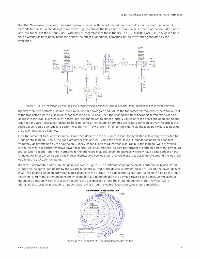
The AWR Microwave Office load-pull wizard provides users with an automated process that is much easier than manual methods for the setup and design of networks. Figure 7 shows the basic setup: a source-pull tuner is at the input (left) and a load-pull tuner is at the output (right), with bias Ts integrated into those tuners. The CGH40010F GaN HEMT device is a bare die, so wirebonds have been included to show the effect of additional parasitics on the waveforms generated by the simulation.
Figure 7: The AWR Microwave Office load-pull wizard enables simulation instead of costly, time-consuming bench measurements
The first step is to perform a source-pull simulation for power gain and PAE at the fundamental frequency, where the output of the transistor, a bare die, is directly connected to a 50Ω load. Next, the second and third harmonic terminations can be loaded into the load-pull wizard, with their load-pull tuners set to either arbitrary values or to the short and open conditions required for Class F. Because transistors have parasitics, the resulting networks will require some adjustment to obtain the desired drain-source voltage and current waveforms. This waveform engineering is done via the load-pull wizard to peak up the power, gain, and efficiency.
After fundamental-frequency source pull has been done with the 50Ω output load, the next step is to change the setup for fundamental load pull. Again, the goals are power gain and PAE using the optimum input impedance point for each test frequency, as determined by the source pull. Finally, second- and third-harmonic source pull and load pull will be invoked within the wizard to further improve power gain and PAE, ensuring that the best performance is obtained from the device. Of course, when second- and third-harmonic terminations are included, their impedances will likely have a small effect on the fundamental impedance. Capabilities in AWR Microwave Office load-pull analysis make it easier to iterate around the load-pull loop to get to that optimum point.
The first-fundamental source-pull for gain is shown in Figure 8. The optimum impedance point is automatically calculated through all the converged points by the wizard. Since the output of the device is terminated in a 50Ω load, the power gain of 15.3dB will change when an optimized load is placed on the output. The blue contours capture the falloff in gain as the input match shifts from the optimum point shown in magenta. Depending upon the device’s reverse isolation (S12), these input impedance contours will shift, possibly requiring the designer to re-tune the input impedance match. AWR software addresses the iterative approach to input/output tuning through synchronized source/load-pull capabilities.
Figure 8: The fundamental-frequency source pull for gain
Load-Pull Analysis for Optimizing PA Performance
8www.cadence.com/go/awr

Figure 9 shows the results for output power, which are actually quite close to those obtained for power gain, even though the output of the device is loaded into 50Ωs. To some extent, this is due to the fact that the intrinsic load line of the device is not that far from 50Ω, as will be seen when fundamental load pull is performed.
Figure 9: Maximum power source impedance very close to maximum gain impedance
Figure 10 shows the fundamental source pull for PAE. Again, the optimum point for PAE has an impedance that is very close to the maximum for both gain and power, which simplifies the matching task considerably. Note that even though the load is directly into 50Ω, the PAE is already over 60% at this point.
Figure 10: Maximum PAE impedance is very close to maximum for both gain and power, which simplifies the matching task
The next step is to perform load-pull analysis for maximum gain (Figure 11), with the source pull set at the impedance that was giving the best PAE. It can be seen that the optimum impedance for gain on the load side of the device in this case is not that far removed from 50Ω—about a two-to-one VSWR.
Figure 11: The optimum impedance for gain on the load side of the device is relatively close to 50Ω
Load-Pull Analysis for Optimizing PA Performance
9www.cadence.com/go/awr

Figure 12 shows the fundamental load-pull results for power and PAE. The result for power is similar to the impedance point for gain, with a small difference seen for the optimal PAE result. The PAE has improved from 60.5% with source pull alone to 72% at this point, with both ports matched for PAE at the fundamental only.
Figure 12: Fundamental load pull for power, similar to the impedance point for gain in Figure 11 and load pull with the source tuner set for optimal PAE from the source-pull data
Using the load-pull wizard, there are several options for source and load-pull optimization at the second and third harmonics. Figure 13 shows the result with the fundamental source and load impedances set to previous values and then allowing the wizard to find the optimum second-harmonic load pull for maximum PAE. In this case, the PAE has improved to over 80%. Adding the third-harmonic load pull (Figure 13 [right]) has a lesser effect, improving PAE by one or two percentage points. The ability to perform source pull and load pull for the device at the second and third harmonics can be used to meet other performance goals. For example, the same kind of optimization can be done to maximize power gain and output power for a particular PA design.
Figure 13: Both ports are loaded for optimal PAE, which improves to >80% when the second harmonic is properly terminated and the third harmonic load-pull result has a smaller effect, providing one or two percentage points improvement in efficiency
Load-Pull Analysis for Optimizing PA Performance
10www.cadence.com/go/awr
Using the Load-Pull Data
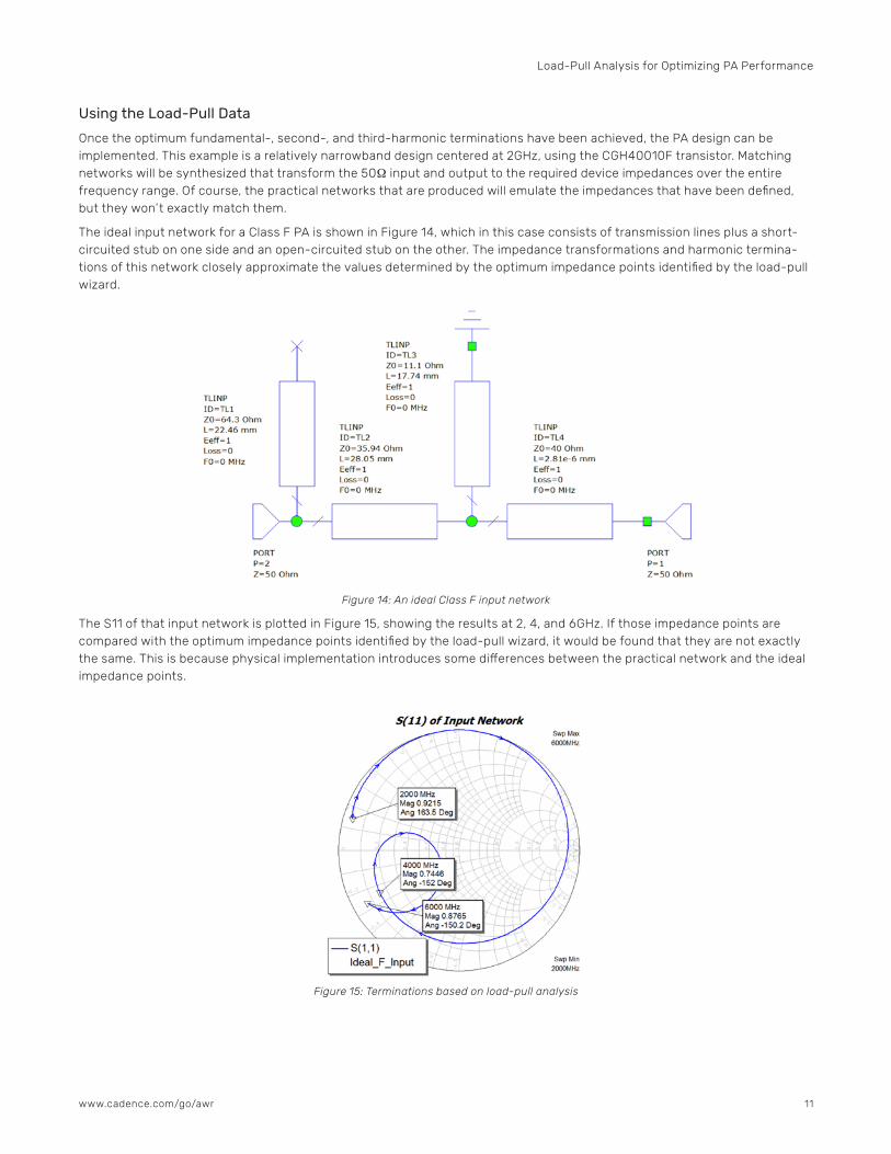
Once the optimum fundamental-, second-, and third-harmonic terminations have been achieved, the PA design can be implemented. This example is a relatively narrowband design centered at 2GHz, using the CGH40010F transistor. Matching networks will be synthesized that transform the 50Ω input and output to the required device impedances over the entire frequency range. Of course, the practical networks that are produced will emulate the impedances that have been defined, but they won’t exactly match them.
The ideal input network for a Class F PA is shown in Figure 14, which in this case consists of transmission lines plus a short-circuited stub on one side and an open-circuited stub on the other. The impedance transformations and harmonic termina-tions of this network closely approximate the values determined by the optimum impedance points identified by the load-pull wizard.
Figure 14: An ideal Class F input network
The S11 of that input network is plotted in Figure 15, showing the results at 2, 4, and 6GHz. If those impedance points are compared with the optimum impedance points identified by the load-pull wizard, it would be found that they are not exactly the same. This is because physical implementation introduces some differences between the practical network and the ideal impedance points.
Figure 15: Terminations based on load-pull analysis
Load-Pull Analysis for Optimizing PA Performance
11www.cadence.com/go/awr

Figure 16 shows an ideal Class F output. The quarter-wave line is also used to provide drain bias for the transistor. In addition, there is an open circuit stub with some transmission-line transformation, so that it is an open at the second harmonic and a short at the third-harmonic.
Figure 16: Harmonic loading: open at second and short at the third
Looking into the input of the network from the reference plane of the device drain, Figure 17 shows the fundamental-, second-, and third-harmonic impedances presented by the network. Again, going back to the wizard, it can be seen that there are some differences between the practical transmission-line-based network and the ideal impedances. In Figure 18, the networks are placed at the input and output of the GaN HEMT device and a simulation of the complete amplifier is run.
Figure 17: Terminations based on load-pull analysis
Figure 18: The complete PA, with input and output networks, gate and drain bias, and the CGH40010F GaN HEMT device
Load-Pull Analysis for Optimizing PA Performance
12www.cadence.com/go/awr

Figure 19 shows the simulated prediction for power gain, output power, and PAE. The results show that PAE reaches a maximum of 84%, which is slightly better than the result predicted by the load-pull wizard.
Figure 19 (right) shows the drain voltage, and current waveforms. As noted earlier, when source and load pull are performed with the load-pull wizard, there will be some degree of waveform engineering. If maximum PAE is requested, the wizard’s optimization algorithms will try to produce the voltage and current waveforms at the transistor that are not only the right shape, but also ideal and anti-phase.
Figure 19: The simulated prediction for power gain, output power, and PAE and voltage and current waveforms
The waveform plot shows an approximate square voltage waveform, or as close as can be obtained by engineering only a few harmonics. The half-sine current waveform is a much better approximation. These waveforms are measured at the device junction, so the effects of parasitics between the device and the model pins are not of concern. The Cree GaN HEMT models shown in Figure 18 have additional pins the allow direct measurement at the junction in order to see the transistor waveforms.
Another feature of this design is in the harmonic content as seen at the output of the amplifier (Figure 20). This is not at the drain of the amplifier, but at the output. From this data, it can be seen that the harmonic terminations are doing their job well as there is very little harmonic content coming through the output of the amplifier. Output power varies by 1 or 2dBm across 200MHz, so it is an inherently narrowband design, as are most Class F PAs. Figure 20 (right) shows the PAE versus frequency and it can be seen that it is in the range of 80+%over about 150 MHz but drops off quickly on either side at 1.9 and 2.05GHz.
Figure 20: At the output, there is >23dB worst-case harmonic rejection, confirming that terminations are working properly and PAE versus frequency; PAE remains relatively constant over 150MHz, but drops off quickly below 1.9 and above 2.05GHz
In conclusion, switching modes of operation for PAs such as Class F and Inverse Class F are becoming more and more popular as designers focus on improving PAE. This is true for a range of applications from radar to wireless telecom. The AWR Microwave Office load-pull wizard and its ability to inspect transistor voltage and current waveforms helps designers gain confidence in their high performance designs and the process of waveform-engineered PA design.
Load-Pull Analysis for Optimizing PA Performance
13www.cadence.com/go/awr

Enhanced Load-Pull Measurements for Base Station PAsThis section examines the power of load-pull simulation for identifying the optimum load and source impedance for an active power device used in a base station PA. With AWR Microwave Office load-pull analysis, performance contours are plotted on a Smith chart, which shows the designer how changing impedances impact the device’s performance (Figure 21).
Figure 21: The load-pull methodology in which the load (or source) impedance of a device is swept and measured, then performance contours are plotted on a Smith chart
The traditional circuit design flow typically involves running a load-pull simulation on a nonlinear model of the device in the circuit design software, as shown in Figure 22.
Figure 22: A traditional design flow, including nonlinear model of the device and load pulling of that model in circuit design software
Load-Pull Analysis for Optimizing PA Performance
14www.cadence.com/go/awr

In this traditional approach, the input and output matching networks are then designed based on load-pull contours from the device model, and performance criteria that are important for the design are plotted. From that point, the designer tweaks the matching networks until all design goals are met or at least optimized to the fullest extent possible.
There are several issues with this traditional design flow. The first problem is overall accuracy of nonlinear models. It is difficult to create a nonlinear model that is accurate over all operating conditions such as bias, frequency, and power level. The second issue is the simple availability of nonlinear models within short design cycle times.
Using Measured Load-Pull Data as a Behavioral Model
To circumvent this, PA designers have begun designing their matching networks and associated circuitry directly from measured load-pull data. This has several advantages, one of which is that the entire process is within the control of the design group itself and data can be regenerated or redefined in-house if necessary, rather than relying on a third party for model generation.
The challenge for electronic design automation (EDA) companies is to provide intuitive methods for dealing with complex swept load-pull data sets. These data sets can include nested harmonic load pull, nested load and source pull, and two-tone excitation, in which intermodulation distortion levels can be analyzed as a function of load impedance. The data can also include multiple fundamental frequencies. As such, an entire array of possibilities exists for manipulating the data, including plotting as a function of frequency, power, bias, load, or source impedance at the fundamental frequency, and load or source impedance at harmonic frequencies. Figure 23 shows a data plotting and manipulation example of contours for fundamental and second harmonic impedances.
Figure 23: Contours for fundamental PAE versus impedance (fundamental and second harmonic)
Measurements to be plotted can include power capability, gain, efficiency, intermodulation distortion levels, AM-PM perfor-mance, or essentially any other performance metric that can be measured on a modern load-pull system. If the device’s internal matching elements and package parasitics are known, measurements can also be de-embedded to the current generator plane of the device, supporting the waveform engineering previously discussed in the Class F amplifier example.
Above and beyond viewing and plotting swept load-pull data, the ability to directly optimize matching networks is of paramount importance. Matching networks that are designed from measured load-pull data enable fast and accurate prototype builds, as the uncertainty of a nonlinear model is removed and replaced with empirical, verifiable data. The challenge for EDA companies in this case is establishing a means of interpolating device performance from load-pull data using the impedances computed from an output matching network. In this way, after the load-pull data has been imported into the circuit design tool, the matching networks can be designed directly.
A final consideration is the ability to produce equivalent data sets from nonlinear models. The circuit design software must be capable of producing data that can be fit to empirical data in order to enable modeling groups to produce accurate device models. In other words, the ability to produce equivalent measurements entirely within the software is necessary in order to provide simulated data sets that can be compared to empirical data. In this way, the circuit simulator can be used not only for data manipulation and circuit design, but also for improving the accuracy of nonlinear device models.
Load-Pull Analysis for Optimizing PA Performance
15www.cadence.com/go/awr

Types of Supported Data in AWR Microwave Office Software
Historically, single-sweep point files such as Maury Microwave LP/SP files and Focus Microwaves LPD files have been supported. AWR Microwave Office software supports multidimensional files such as Maury SPL, Maury CST, and Focus LPD, which have swept data. With AWR software, the denser the data sets (gamma points, frequencies, power steps), the better the focus is on seamless, intuitive post-processing of data (Figure 24).
Figure 24: In AWR software, the more dense the data sets, the better the focus is on post-processing of data
The load-pull formats in AWR Microwave Office software give designers access to an extensive array of data manipulation possibilities. Figure 25 shows on the left a rectangular graph of the input power versus the index. There is a marker that points to a specific input power and the contours for that power level are being plotted on the right. If the marker is moved, another set of contours is obtained that correspond to that power level. If the marker is moved again, a third set of contours is obtained. This is something that can’t be done with older single-point local files and enables designers to quickly visualize how load contours change with any parameter, in this case input power.
Figure 25: The rectangular graph on the left shows the input power versus index; a marker points to a specific input power and plots the contours in the Smith chart —when the marker is moved, a new set of contours is plotted
Load-Pull Analysis for Optimizing PA Performance
16www.cadence.com/go/awr
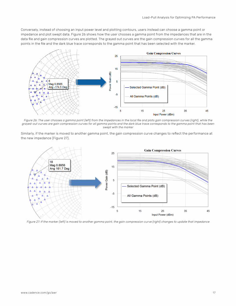
Conversely, instead of choosing an input power level and plotting contours, users instead can choose a gamma point or impedance and plot swept data. Figure 26 shows how the user chooses a gamma point from the impedances that are in the data file and gain compression curves are plotted. The grayed out curves are the gain compression curves for all the gamma points in the file and the dark blue trace corresponds to the gamma point that has been selected with the marker.
Figure 26: The user chooses a gamma point (left) from the impedances in the local file and plots gain compression curves (right), while the grayed-out curves are gain compression curves for all gamma points and the dark blue trace corresponds to the gamma point that has been
swept with the marker
Similarly, if the marker is moved to another gamma point, the gain compression curve changes to reflect the performance at the new impedance (Figure 27).
Figure 27: If the marker (left) is moved to another gamma point, the gain compression curve (right) changes to update that impedance
Load-Pull Analysis for Optimizing PA Performance
17www.cadence.com/go/awr

Design Flows Using AWR Software Load-Pull Capabilities
What would a typical design flow look like using the load-pull capabilities in AWR software? Figure 28 shows the impedance points being plotted for a 2.1GHz, 80W (P1dB power level) laterally diffused metal-oxide semiconductor (LDMOS) device. A gamma point has been chosen and the AM-PM and gain compression curve is plotted for three frequencies that are in the file (2.11GHz, 2.14GHz, and 2.17GHz). The 2dB gain compression power capability is also plotted in tabular format.
Figure 28: Impedance points and selected gamma point plotted for a 2.1GHz, 80W LDMOS device
Figure 29 shows how users can move the marker around, select different gamma points, and parse through the performance space of the device, assessing tradeoffs as they go. If another impedance point is chosen, a new set of curves is automati-cally generated that corresponds to that load impedance, as well as another set of AM-PM and gain compression curves, and another 2dB power figure.
Figure 29: Users can move the marker around, use different gamma points, and parse through the performance space of the device, assessing tradeoffs as they go
Load-Pull Analysis for Optimizing PA Performance
18www.cadence.com/go/awr

Designers can do this until they reach what they consider their optimum desired impedance for their design goals. In Figure 30, another gamma point has been chosen that has a very flat gain compression, very flat AM-PM, and the 2dB power that is now close to 100W.
Figure 30: Another gamma point has been chosen that has a very flat gain compression, very flat AM-AM/AM-PM, and the 2dB power is close to 100W
Another capability in AWR software enables something called an “overlap contour.” Figure 31 shows general contours for output power and PAE, along with the overlap contour for specific output power and PAE levels. 50dBm power capability and 70% PAE have been chosen, and the overlap contour shows the tiny locus of impedances where both of these design criteria are being met.
Figure 31: Overlap contour for design criteria of 50dBm power and 70% PAE
Base station designers are never designing for just one target. When there are multiple performance criteria that must be met simultaneously, this measurement helps the designer narrow in very quickly using specific performance criteria to the locus of impedances where both criteria are reached simultaneously.
An additional point to make here is that just because users are sweeping input power doesn’t mean they are constrained to making all their measurements based on input power. If designers are interested in plotting contours or designing in terms of output power or gain compression level as most people do, they can simply take input power sweeps and use the capability in AWR software to easily plot output power-based or gain compression-based contours.
Load-Pull Analysis for Optimizing PA Performance
19www.cadence.com/go/awr

Figure 32 shows three curves of the actual gain compression value going up to about 6dB gain compression at three frequencies. The center band at 2.14GHz and a 3dB compression point is chosen, then the contours can be plotted for whatever measurements the designer chooses. In this figure, the user has stuck with the PAE and output power capability contours.
Figure 32: The left graph shows three curves of actual gain compression values going up to about 6dB gain compression at three frequencies, and the right chart shows the PAE at 3dB gain compression
Additionally, matching networks can be optimized directly from the load-pull data itself. In Figure 33, output power capability, gain, and PAE have been plotted, this time as a function of frequency. The matching networks can be tuned or optimized based directly on these performance criteria. Note that the software enables users to tune directly, or optimize using a wide variety of included optimization algorithms. The bars in the figure are the goals for the optimizer. Once goals have been set, the optimization runs on the matching network to meet the desired performance, and the physical parameters for the matching network are updated.
Figure 33: Several performance criteria have been plotted, and matching networks can be optimized based directly on them
Load-Pull Analysis for Optimizing PA Performance
20www.cadence.com/go/awr

Figure 34 shows the result of the optimization and the updated matching network. The goals can easily be modified to further optimize the design, and the matching network parameters will be updated based on the optimization result. This ability to optimize directly from the local performance data file itself is a very powerful concept.
Figure 34: Performing the optimization based on empirical load-pull data updates the matching network’s physical parameters
Load pull will continue to be an integral part of the design flow for microwave and RF power devices for the foreseeable future. The swept format files combined with EDA vendors updating their capabilities has served to encourage the use of load pull. For an empirical-based design, load-pull measurement/modeling has lowered the dependency on outside factors and increased the design group’s control. Designers can go back and tell their load-pull group to take more data points, different gamma points, or different power levels, making the design cycle more closed loop and enabling quicker feedback rather than waiting for nonlinear device models to be created. The collection of a rich load-pull data set can shorten design cycles, particularly with swept input power. The AWR Design Environment platform provides enough flexibility in interacting with load-pull data that users have the ability to choose whatever is best for each design project and/or design with their own use models.
Load-Pull Analysis for Optimizing PA Performance
21www.cadence.com/go/awr

Synchronized Source/Load-Pull AnalysisA rich set of load-pull data provides PA designers with the means to investigate the optimum capability of a communication device in relation to design goals and performance targets. To fully benefit from this information, designers need an intuitive method for working with complex swept load-pull data sets. These data sets can include multiple fundamental frequencies, nested harmonic load pull, and/or nested source and load pull. As such, PA performance can easily be understood across multiple operating conditions.
Measurements can include available output power, gain, efficiency, intermodulation distortion levels, or, essentially, any other performance metric that can be measured on a modern load-pull system. The measurements can be readily de-embedded to the current generator reference plane of the device, which is a critical consideration for any designer moving beyond the traditional reduced conduction angle classes of operation.
This section describes how load-pull data files with an independent swept parameter such as power can be used directly in AWR Microwave Office software. The design of a Class J PA is used as an example to show how the load-pull data can be used to complement traditional, theoretical Class J analyses and streamline the design flow.
As advanced load-pull measurement systems gain in popularity, increasingly sophisticated capabilities have been added to AWR Microwave Office in order to help designers deal with more and more complex sets of load-pull data. Strategic use of these tools streamlines the overall PA design flow, enabling designers to eliminate guesswork and post-fabrication “tweaking” from their first-cut prototypes. The same load-pull capabilities can be applied to simulated compact device models.
Device Model and Design Goals
This example is based on a Qorvo T2G6000528-Q3 GaN on silicon carbide (SiC) HEMT device with approximately 10W at P3dB power compression and 28V of drain voltage operation. The bias point is Class B or very heavy Class AB (Figure 35).
Figure 35: 10W at P3dB and 28V drain voltage operation, Class B behavior with dynamic load line shown
Load-Pull Analysis for Optimizing PA Performance
22www.cadence.com/go/awr
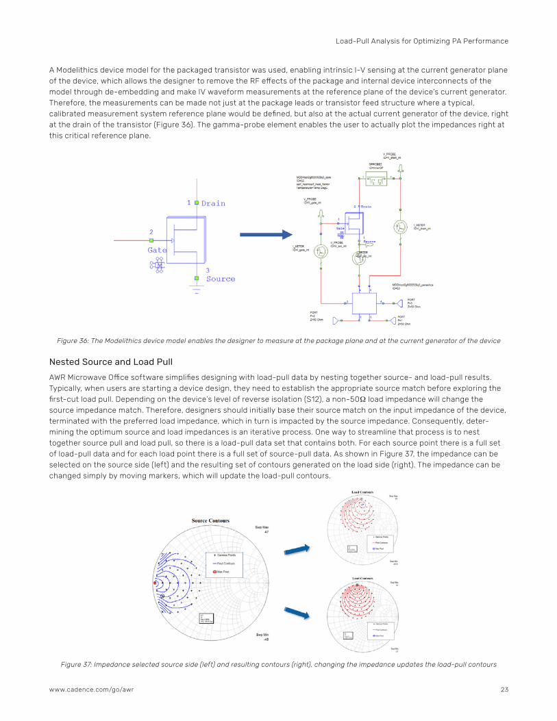
A Modelithics device model for the packaged transistor was used, enabling intrinsic I-V sensing at the current generator plane of the device, which allows the designer to remove the RF effects of the package and internal device interconnects of the model through de-embedding and make IV waveform measurements at the reference plane of the device’s current generator. Therefore, the measurements can be made not just at the package leads or transistor feed structure where a typical, calibrated measurement system reference plane would be defined, but also at the actual current generator of the device, right at the drain of the transistor (Figure 36). The gamma-probe element enables the user to actually plot the impedances right at this critical reference plane.
Figure 36: The Modelithics device model enables the designer to measure at the package plane and at the current generator of the device
Nested Source and Load Pull
AWR Microwave Office software simplifies designing with load-pull data by nesting together source- and load-pull results. Typically, when users are starting a device design, they need to establish the appropriate source match before exploring the first-cut load pull. Depending on the device’s level of reverse isolation (S12), a non-50Ω load impedance will change the source impedance match. Therefore, designers should initially base their source match on the input impedance of the device, terminated with the preferred load impedance, which in turn is impacted by the source impedance. Consequently, deter-mining the optimum source and load impedances is an iterative process. One way to streamline that process is to nest together source pull and load pull, so there is a load-pull data set that contains both. For each source point there is a full set of load-pull data and for each load point there is a full set of source-pull data. As shown in Figure 37, the impedance can be selected on the source side (left) and the resulting set of contours generated on the load side (right). The impedance can be changed simply by moving markers, which will update the load-pull contours.
Figure 37: Impedance selected source side (left) and resulting contours (right), changing the impedance updates the load-pull contours
Load-Pull Analysis for Optimizing PA Performance
23www.cadence.com/go/awr
Conversely, on the device output, the load impedance point can be selected and the resulting source-pull contours will be shown on the right. Again, the source-pull contours are updated by moving the data marker amongst data points on the device’s load reference plane.
This powerful feature eliminates the need to perform iterative simulations with different source/load terminations in order to define the input and output target impedances. It is all there in one data set.
Load Pull with Frequency
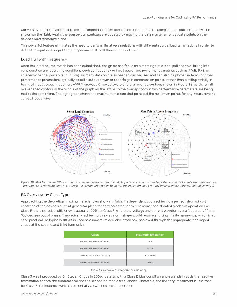
Once the initial source match has been established, designers can focus on a more rigorous load-pull analysis, taking into consideration any operating conditions such as frequency or input power and performance metrics such as P1dB, PAE, or adjacent-channel power-ratio (ACPR). As many data points as needed can be used and can also be plotted in terms of other performance parameters, typically specific output power or specific gain compression points, rather than plotting strictly in terms of input power. In addition, AWR Microwave Office software offers an overlap contour, shown in Figure 38, as the small oval-shaped contour in the middle of the graph on the left. With the overlap contour two performance parameters are being met at the same time. The right graph shows the maximum markers that point out the maximum points for any measurement across frequencies.
Figure 38: AWR Microwave Office software offers an overlap contour (oval shaped contour in the middle of the graph) that meets two performance parameters at the same time (left), while the maximum markers point out the maximum point for any measurement across frequencies (right)
PA Overview by Class Type
Approaching the theoretical maximum efficiencies shown in Table 1 is dependent upon achieving a perfect short-circuit condition at the device’s current generator plane for harmonic frequencies. In more sophisticated modes of operation like Class F, the theoretical efficiency is actually 100% for Class F, where the voltage and current waveforms are “squared off” and 180 degrees out of phase. Theoretically, achieving this waveform shape would require shorting infinite harmonics, which isn’t at all practical, so typically 88.4% is used as a maximum available efficiency, achieved through the appropriate load imped-ances at the second and third harmonics.
Table 1: Overview of theoretical efficiency
Class J was introduced by Dr. Steven Cripps in 2006. It starts with a Class B bias condition and essentially adds the reactive termination at both the fundamental and the second harmonic frequencies. Therefore, the linearity impairment is less than for Class E, for instance, which is essentially a switched-mode operation.
Class Maximum Efficiency
Class A Theoretical Efficiency 50%
Class B Theoretical Efficiency 78.5%
Class AB Theoretical Efficiency 50 – 78.5%
Class F Theoretical Efficiency 88.4%
Load-Pull Analysis for Optimizing PA Performance
24www.cadence.com/go/awr

What does this mean in terms of the waveform shape? Figure 39 shows the Class B waveforms on the left and the Class J waveforms on the right.
Figure 39: Class B waveforms (left) and Class J waveforms (right).
Class B, as noted previously, is at 180-degree conduction cycle. For the Class J waveforms, some harmonic content has been added, the current waveform is essentially squared off, and the time when the device has a positive voltage and is also conducting is minimized. The Class Btheoretical efficiency can be reached without having to have short-circuit conditions at harmonic frequencies, which provides a much more practical approach.
Harmonic Load Pull
How does this fit in with load pull? Apart from fundamental load pull, AWR Microwave Office software enables designers to perform load-pull analysis that includes load-pull contours based on termination impedances at harmonic frequencies. This allows them to quickly assess the impact of controlling second- and third-harmonic terminations on PA performance. Figure 40 shows a fixed fundamental termination on the load side with the second-harmonic termination essentially being pulled around the entire Smith chart. PAE contours can be plotted, which show the efficiency of the device based on its harmonic terminations and identify an area of the Smith chart where efficiency is maximized.
Figure 40: Harmonic load pull can be used to assess the impact of controlling the second- and third-harmonic terminations and easily establish an area of the Smith chart (blue arrow) for harmonic impedances to maximize device performance
Load-Pull Analysis for Optimizing PA Performance
25www.cadence.com/go/awr
De-Embedding and Waveforms
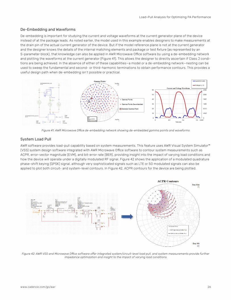
De-embedding is important for studying the current and voltage waveforms at the current generator plane of the device instead of at the package leads. As noted earlier, the model used in this example enables designers to make measurements at the drain pin of the actual current generator of the device. But if the model reference plane is not at the current generator and the designer knows the details of the internal matching elements and package or test fixture (as represented by an S-parameter block), that knowledge can also be applied in AWR Microwave Office software by using a de-embedding network and plotting the waveforms at the current generator (Figure 41). This allows the designer to directly ascertain if Class J condi-tions are being achieved. In the absence of either of these capabilities—a model or a de-embedding network—nesting can be used to sweep the fundamental and second- or third-harmonic terminations to obtain performance contours. This provides a useful design path when de-embedding isn’t possible or practical.
Figure 41: AWR Microwave Office de-embedding network showing de-embedded gamma points and waveforms
System Load Pull
AWR software provides load-pull capability based on system measurements. This feature uses AWR Visual System Simulator™ (VSS) system design software integrated with AWR Microwave Office software to contour system measurements such as ACPR, error-vector magnitude (EVM), and bit-error rate (BER), providing insight into the impact of varying load conditions and how the device will operate under a digitally modulated RF signal. Figure 42 shows the application of a modulated quadrature phase-shift keying (QPSK) signal, although very sophisticated signals such as LTE or 5G modulated signals can also be applied to plot both circuit- and system-level contours. In Figure 42, ACPR contours for the device are being plotted.
Figure 42: AWR VSS and Microwave Office software offer integrated system/circuit-level load pull, and system measurements provide further impedance optimization and insight to the impact of varying load conditions
Load-Pull Analysis for Optimizing PA Performance
26www.cadence.com/go/awr

System load pull offers the same functionality as using circuit-level load pull with an expansion of measurements commonly used in communication systems. As with circuit measurements, system measurements can be referenced to a specific output power level or any other operating condition or measurement, (Figure 43), and are not limited to simply a function of the input power.
Figure 43: As with circuit measurements, system-level measurements can be referenced to a specific output power level
Load pull is and will continue to be an integral part of most design flows for high-power amplifiers, whether it be load-pulling device models or measured load-pull files. The unique functionality of nesting source- and load-pull contours in the AWR Design Environment platform can significantly shorten the time required to design an amplifier by streamlining the iterative process of determining the appropriate impedances to present to the device’s input and output terminals. De-embedding and waveform plotting is useful for understanding if the matching circuit is performing the necessary waveform shaping (squaring off) to improve amplifier efficiency. Nested fundamental/harmonic load-pull contours can be used in the cases where studying the waveform at the device model’s current generator isn’t practical. In addition, system-level load pull provides an additional powerful design option for engineers studying performance tradeoffs based on system measurements such as ACPR, EVM, and BER for amplifiers operating under digitally modulated RF signals.
Load-Pull Analysis for Optimizing PA Performance
27www.cadence.com/go/awr

ConclusionFor successful designs, PA designers must determine the ideal output load for system-driven amplifier requirements such as output power, efficiency, and linearity. The AWR Design Environment platform provides integrated technologies for circuits, layouts, and EM field analysis that enable designers to investigate the optimum capability of their communication device in relation to design goals and performance targets. This white paper has presented application examples that showcase the load-pull analysis capabilities in AWR Microwave Office software, including analysis of simple circuits, matching circuits, and circuit optimization, as well as simulation of wideband high-efficiency PAs, load-pull measurements for base station PAs, and synchronized source/load-pull analysis.
Load-Pull Analysis for Optimizing PA Performance
Cadence is a pivotal leader in electronic design and computational expertise, using its Intelligent System Design strategy to turn design concepts into reality. Cadence customers are the world’s most creative and innovative companies, delivering extraordinary electronic products from chips to boards to systems for the most dynamic market applications. www.cadence.com
© 2021 Cadence Design Systems, Inc. All rights reserved worldwide. Cadence, the Cadence logo, and the other Cadence marks found at www.cadence.com/go/trademarks are trademarks or registered trademarks of Cadence Design Systems, Inc. All other trademarks are the property of their respective owners. 15681 01/21 DB/SA/WP-LDPL-PA/PDF