localized effect of pbi2 excess in perovskite solar cells
TRANSCRIPT
This is a repository copy of Localized effect of PbI2 excess in perovskite solar cells probedby high- resolution chemical- optoelectronic mapping.
White Rose Research Online URL for this paper:http://eprints.whiterose.ac.uk/142115/
Version: Accepted Version
Article:
Barbe, J., Newman, M., Lilliu, S. orcid.org/0000-0002-8449-2211 et al. (6 more authors) (2018) Localized effect of PbI2 excess in perovskite solar cells probed by high- resolution chemical- optoelectronic mapping. Journal of Materials Chemistry A, 6 (45). pp. 23010-23018. ISSN 2050-7488
https://doi.org/10.1039/c8ta09536a
© The Royal Society of Chemistry 2018. This is an author produced version of a paper subsequently published in Journal of Materials Chemistry A. Uploaded in accordance with the publisher's self-archiving policy.
[email protected]://eprints.whiterose.ac.uk/
Reuse
Items deposited in White Rose Research Online are protected by copyright, with all rights reserved unless indicated otherwise. They may be downloaded and/or printed for private study, or other acts as permitted by national copyright laws. The publisher or other rights holders may allow further reproduction and re-use of the full text version. This is indicated by the licence information on the White Rose Research Online record for the item.
Takedown
If you consider content in White Rose Research Online to be in breach of UK law, please notify us by emailing [email protected] including the URL of the record and the reason for the withdrawal request.
Journal Name
ARTICLE
This journal is © The Royal Society of Chemistry 20xx J. Name., 2013, 00, 1-3 | 1
Please do not adjust margins
Please do not adjust margins
Received 00th January 20xx,
Accepted 00th January 20xx
DOI: 10.1039/x0xx00000x
www.rsc.org/
Localized effect of PbI2 excess in perovskite solar cells probed by
high-resolution chemical-optoelectronic mapping
Jérémy Barbéa, Michael Newmana, Samuele Lilliub, Vikas Kumarc, Harrison Ka Hin Leea, Cécile Charbonneaua, Cornelia
Rodenburgc, David Lidzeyb and W.C. Tsoia
We report the laser irradiation of CH3NH3PbI3 solar cells to generate and control localized PbI2 degradation product. We
show that by tuning the laser power and illumination time, we can controllably form a local excess of PbI2. High-resolution
advanced multi-mapping techniques are used to highlight the effect of PbI2 on the photophysical and photoelectrical
properties in a complete perovskite device. Whereas a thick PbI2 film at the perovskite/hole transport layer interface has a
detrimental effect on the photocurrent and photoluminescence, a thin PbI2 film (<20 nm) leads to a significant photocurrent
increase, which is ascribed to the passivation of non-radiative defects and reduced charge recombination at the interface.
Our findings reveal that laser irradiation is a new approach to understand the effect of PbI2 surface layers and potentially
offers a means to passivate trap states and improve PV properties of perovskite devices.
a. SPECIFIC - Swansea University, Bay Campus, Fabian Way, Swansea, SA1 8EN, U.K. b. Department of Physics and Astronomy, The University of Sheffield, Hicks Building,
Hounsfield Road, Sheffield S3 7RH, U.K. c. Department of Materials Science and Engineering, University of Sheffield, Mappin
Street, Sheffield S1 3JD, U.K
ARTICLE Journal Name
2 | J. Name., 2012, 00, 1-3 This journal is © The Royal Society of Chemistry 20xx
Please do not adjust margins
Please do not adjust margins
INTRODUCTION
Perovskites have generated tremendous interest because of their
excellent optoelectronic properties such as high absorption
coefficient1, long carrier lifetime, high carrier mobility2 and tolerance
to defects3. Intense research effort has led to a dramatic rise in power
conversion efficiency (PCE) of perovskite solar cells (PSCs)4. However,
despite rapid progress, record PCEs are still far from the Shockley-
Queisser limit5 which suggests that non-radiative recombination plays
a key role in the overall efficiency loss. Furthermore, stability issues
remain a major challenge for PSCs that needs to be fully addressed
before perovskite devices can reach the market6.
The stoichiometry of perovskites has been shown to have a significant
impact on device performance. Several studies have investigated the
effect of non-stoichiometric perovskite films containing a deficiency
or excess of PbI27,8,9,10,11,12. The general trend is that a slight excess of
PbI2 is usually beneficial to device performance. This has been
observed not only for standard methylammonium lead iodide
(CH3NH3PbI3) devices13 but also for mixed perovskites such as
(FAPbI3)0.85(MAPbBr3)0.1514. High performance PSCs with more than
21% PCE have been obtained using a triple cation perovskite
containing some excess lead iodide15. Two main routes have been
used to obtain excess PbI2 phase in the perovskite layer. The first route
induces the crystallization of CH3NH3PbI3 from a non-stoichiometric
PbI2:CH3NH3I ratio. This can be achieved using a one-step synthesis
method in which the PbI2:CH3NH3I ratio is tuned directly in the
precursor solution9. However, changing the composition of the
precursor solution from under-stoichiometric (PbI2 deficient) to over-
stoichiometric (PbI2 excess) can affect the size of the perovskite
crystallites formed10, a feature that complicates the interpretation of
the role of embedded PbI2 phase. A two-step synthesis method has
also been used where PbI2 is first deposited and subsequently exposed
to the methylammonium iodide16,11,17,18. Here, the overall
stoichiometry depends on the length of the second step, as shorter
exposure times result in incomplete conversion of PbI2 to CH3NH3PbI3.
However, this method usually leads to a less precise control of the
film.
The second route uses post-deposition thermal annealing to generate
PbI2 in the already formed CH3NH3PbI3 film19,13. Thermal annealing
induces the decomposition of the perovskite phase to PbI2, which
amount can be controlled by adjusting the annealing time or
temperature. Using this method, Du et al. showed that the PbI2 that
forms at grain boundary regions can have a positive effect on device
performance, by reducing current-voltage hysteresis and increasing
the PCE19. However, at higher annealing temperatures, excessive
formation of PbI2 causes resistive losses and poor device performance.
Chen et al. reported similar PbI2 passivation effect after annealing the
perovskite film at 150°C for 60 min, but found that longer annealing
times deteriorated device performance by introducing excessive
PbI213. One of the drawbacks of such post-deposition thermal
annealing processes is the limited control over the amount of PbI2 that
is formed. Furthermore, thermal annealing can also induce secondary
effects via modification of the perovskite film crystalline structure.
The reasons for the apparently beneficial effect of a PbI2 excess are
still unclear. Several groups have suggested more favourable energy
alignments of the perovskite layer with electron and hole transport
layers. Here, it was proposed that PbI2 can form a type I band
alignment with the perovskite, resulting in more efficient charge
extraction by energy band matching and decreased interfacial
recombination9,13. Since PbI2 was observed to preferentially form at
grain boundaries, it was also proposed that a small amount of PbI2 can
passivate grain boundaries, resulting in reduced ion migration10,8,
increased shunt resistance and decreased non-radiative losses19,14.
However, a consensus on the beneficial role of PbI2 has not been
reached with recent studies suggesting that residual PbI2 is not
required to obtain high performance PSCs, but instead reduces device
stability20,12. These conflicting results may well arise due to the high
sensitivity of PSCs to the precise amount and location of PbI2 phase in
the active layer. In general, the techniques used to control PbI2
concentration do not provide sufficiently precise control, with small
variations in PbI2 levels having potentially dramatic effects on device
operation. Furthermore, such techniques also do not afford any
control over the location of excess PbI2, with PbI2 believed to form
homogeneously throughout the depth of the film. It would clearly be
preferential to have control over the location of excess PbI2, as this
could for example allow band alignment/engineering or passivation
mechanisms to be exploited at the interfaces of the perovskite layer
with the different charge-transporting layers.
To address such issues, we report a laser-induced mechanism that
permits precise control over the generation of PbI2 in a perovskite
device stack. We show that when a perovskite device in air is exposed
to a laser beam, it is possible to induce a localized structural
conversion from CH3NH3PbI3 to PbI2, with this process being finely
controlled by adjusting laser power and illumination time. This
Journal Name ARTICLE
This journal is © The Royal Society of Chemistry 20xx J. Name., 2013, 00, 1-3 | 3
Please do not adjust margins
Please do not adjust margins
technique is used to pattern regions having different PbI2 content on
the same sample with micrometer scale resolution, without modifying
crystal structure or grain size. Furthermore, this technique also
preferentially generates PbI2 at the surface of the perovskite (at the
interface with the HTL in the inverted device configuration); a feature
that may allow a better understanding of the role of PbI2 at this
specific interface to be gained.
A number of groups have used mapping techniques to correlate
spatial heterogeneity in lead halide perovskite materials to device
performance14,21. For example, Eperon et al. found that photocurrent
and photoluminescence measurements could be used to understand
how the nature of charge-extracting contacts affect recombination
losses in a full device structure22. However, such techniques do not
provide direct information on the chemical or structural properties of
the perovskite and need to be interpreted with caution. In our
previous work, it was shown that the distribution of PbI2 degradation
products can be measured with micrometer spatial resolution using
Raman spectroscopy (RS)23. In this paper, we use RS in combination
with photocurrent and photoluminescence mapping to
unambiguously correlate the local presence of PbI2 with variations in
photophysical and photoelectrical properties in a PSC. Results show
that a thin PbI2 film (< 20 nm) is formed at the perovskite/HTL interface
which enhances the photocurrent by passivating defect-states and
reducing carrier recombination. The advanced mapping techniques
combined with electron microscopy measurements highlight the role
played by a localized excess of PbI2 in a PSC; a result that would be
difficult to obtain using other characterization methods.
RESULTS
Excess PbI2 generated by laser irradiation of perovskite solar cells.
All experiments were performed on inverted perovskite solar cells
based on the structure glass/ITO/NiOx/CH3NH3PbI3/PCBM/BCP/Ag,
where NiOx is used as a hole transport layer (HTL) and PCBM/BCP as
an electron transport layers (ETL). A laser used to generate Raman
scattering was also used to deliberately accelerate and control the
degradation of the perovskite film within the device stack by varying
the laser power and illumination time. The irradiation of samples was
performed from the glass side, with the laser light penetrating the
device through the transparent ITO and NiOx layers and being
absorbed within the perovskite layer. All irradiation experiments were
carried out in air, however photocurrent-PL-Raman maps were
acquired under a N2 atmosphere to avoid any further degradation by
the laser.
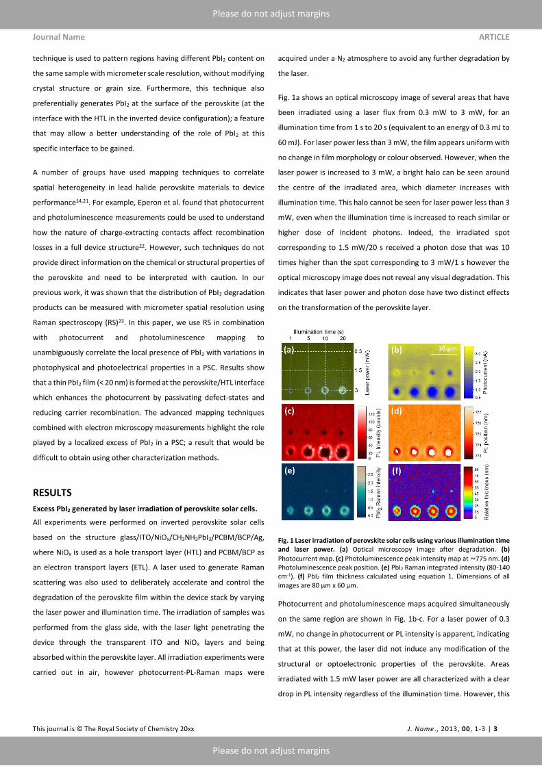
Fig. 1a shows an optical microscopy image of several areas that have
been irradiated using a laser flux from 0.3 mW to 3 mW, for an
illumination time from 1 s to 20 s (equivalent to an energy of 0.3 mJ to
60 mJ). For laser power less than 3 mW, the film appears uniform with
no change in film morphology or colour observed. However, when the
laser power is increased to 3 mW, a bright halo can be seen around
the centre of the irradiated area, which diameter increases with
illumination time. This halo cannot be seen for laser power less than 3
mW, even when the illumination time is increased to reach similar or
higher dose of incident photons. Indeed, the irradiated spot
corresponding to 1.5 mW/20 s received a photon dose that was 10
times higher than the spot corresponding to 3 mW/1 s however the
optical microscopy image does not reveal any visual degradation. This
indicates that laser power and photon dose have two distinct effects
on the transformation of the perovskite layer.
Fig. 1 Laser irradiation of perovskite solar cells using various illumination time
and laser power. (a) Optical microscopy image after degradation. (b)
Photocurrent map. (c) Photoluminescence peak intensity map at ခ775 nm. (d) Photoluminescence peak position. (e) PbI2 Raman integrated intensity (80-140 cm-1). (f) PbI2 film thickness calculated using equation 1. Dimensions of all キマ;ェWゲ ;ヴW Βヰ ´マ ┝ ヶヰ ´マく
Photocurrent and photoluminescence maps acquired simultaneously
on the same region are shown in Fig. 1b-c. For a laser power of 0.3
mW, no change in photocurrent or PL intensity is apparent, indicating
that at this power, the laser did not induce any modification of the
structural or optoelectronic properties of the perovskite. Areas
irradiated with 1.5 mW laser power are all characterized with a clear
drop in PL intensity regardless of the illumination time. However, this
ARTICLE Journal Name
4 | J. Name., 2012, 00, 1-3 This journal is © The Royal Society of Chemistry 20xx
Please do not adjust margins
Please do not adjust margins
either results in an increase in photocurrent (for 1 s irradiation) or a
decrease in photocurrent (10 に 20 s irradiation). For a laser power of
3 mW, we find that all degraded spots are associated with a clear
decrease in photocurrent (Fig. 1b), however a halo of slightly higher
photocurrent (as compared to the surrounding non-irradiated
perovskite) appear at the periphery of irradiated areas. Interestingly,
the PL map also indicates a strong decrease in PL emission intensity
from the centre of the irradiated spots, which is also surrounded by a
halo region from which there is increased emission intensity. This
demonstrates that the photo-degradation of the perovskite device by
the laser beam is highly dependent on the laser power and
illumination time; a process that leads to non-uniform modifications
of the optoelectronic properties of the perovskite. Under strong
irradiation conditions, a highly degraded region is formed that is
characterized by very low PL emission and low photocurrent. This is
surrounded by a halo of high photocurrent and high
photoluminescence intensity.
Then, Raman mapping were performed on the irradiated regions and
plot in Fig. 1e the integrated Raman intensity between 80 cm-1 and
140 cm-1, a range which includes the two main peaks of PbI2 at 96 cm-
1 and 110 cm-1,23 so that the bright regions of the map reveal areas
with high PbI2 content. It is apparent that the spots treated with 3 mW
laser power show PbI2-rich halo shapes of external diameter
comparable to regions characterised with low PL (Fig. 1c) and low
photocurrent (Fig. 1b). However when irradiated by the 1.5 mW
power laser, the presence of PbI2 in the perovskite film can only just
be detected for illumination times of at least 10 s. Interestingly,
changes can be observed by PL and photocurrent mapping from spots
that have been exposed using shorter illumination times (< 10 s at 1.5
mW). This indicates that the PL and photocurrent techniques are more
sensitive to the photodegradation of the buried perovskite film than
is Raman spectroscopy (RS). We note that RS provides direct
information regarding the main degradation product of the perovskite
(PbI2), however photoluminescence emission can be challenging to
interpret when measuring a device as a number of competing
mechanisms may occur simultaneously. For example, free charges in
a device at short-circuit will quench the PL13, however passivation of
non-radiative recombination centers can have the opposite effect and
induce an increase in PL intensity24,9. For this reason, the simultaneous
use of photocurrent mapping and Raman mapping is key to
understand the physical and chemical changes that happen in a
perovskite device as a result of optical irradiation.
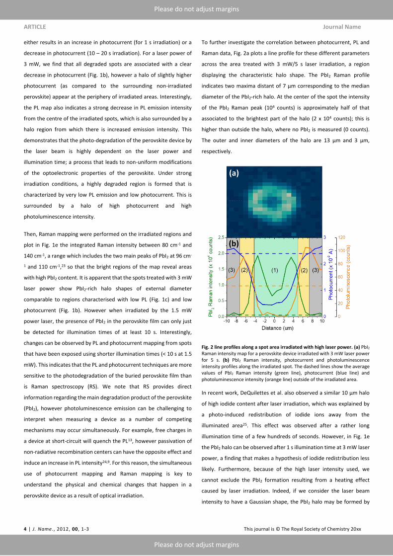
To further investigate the correlation between photocurrent, PL and
Raman data, Fig. 2a plots a line profile for these different parameters
across the area treated with 3 mW/5 s laser irradiation, a region
displaying the characteristic halo shape. The PbI2 Raman profile
キミSキI;デWゲ デ┘ラ マ;┝キマ; Sキゲデ;ミデ ラa Α ´マ IラヴヴWゲヮラミSキミェ デラ デエW マWSキ;ミ
diameter of the PbI2-rich halo. At the center of the spot the intensity
of the PbI2 Raman peak (104 counts) is approximately half of that
associated to the brightest part of the halo (2 x 10⁴ counts); this is
higher than outside the halo, where no PbI2 is measured (0 counts).
TエW ラ┌デWヴ ;ミS キミミWヴ Sキ;マWデWヴゲ ラa デエW エ;ノラ ;ヴW ヱン ´マ ;ミS ン ´マが
respectively.
Fig. 2 line profiles along a spot area irradiated with high laser power. (a) PbI2 Raman intensity map for a perovskite device irradiated with 3 mW laser power for 5 s. (b) PbI2 Raman intensity, photocurrent and photoluminescence intensity profiles along the irradiated spot. The dashed lines show the average values of PbI2 Raman intensity (green line), photocurrent (blue line) and photoluminescence intensity (orange line) outside of the irradiated area.
In recent work, DeQuilettes et ;ノく ;ノゲラ ラHゲWヴ┗WS ; ゲキマキノ;ヴ ヱヰ ´マ エ;ノラ
of high iodide content after laser irradiation, which was explained by
a photo-induced redistribution of iodide ions away from the
illuminated area25. This effect was observed after a rather long
illumination time of a few hundreds of seconds. However, in Fig. 1e
the PbI2 halo can be observed after 1 s illumination time at 3 mW laser
power, a finding that makes a hypothesis of iodide redistribution less
likely. Furthermore, because of the high laser intensity used, we
cannot exclude the PbI2 formation resulting from a heating effect
caused by laser irradiation. Indeed, if we consider the laser beam
intensity to have a Gaussian shape, the PbI2 halo may be formed by
Journal Name ARTICLE
This journal is © The Royal Society of Chemistry 20xx J. Name., 2013, 00, 1-3 | 5
Please do not adjust margins
Please do not adjust margins
the beam tails provided they have sufficient intensity to degrade the
perovskite to PbI2. At the center of the spot, the PbI2 could further
decompose into a third phase, possibly polyiodide compounds26,
which would explain the non-gaussian shape of the PbI2 Raman
profile.
The formation of PbI2 after laser irradiation can be correlated with
variations in photocurrent and PL intensity. In Fig. 2b, we observe that
the PL intensity and photocurrent drop in all areas of high PbI2
intensity (region 1), which is ascribed to reduced perovskite content
and high series resistance of PbI2 in this region. Interestingly, the
ノラ┘Wゲデ ┗;ノ┌W ラa ヮエラデラI┌ヴヴWミデ キゲミげデ ミ┌ノノが キミaWヴヴキミェ デエat the cell stack
remains functional over the entire laser-treated spot area. In region of
moderate PbI2 content (region 2), the PL raises significantly to reach
up to twice the average value of the PL in non-degraded regions,
whereas the photocurrent is still reduced as compared to the average
value, thus showing a high PL-low photocurrent anticorrelation. Then,
in region of low PbI2 content, immediately adjacent to the PbI2 halo
(region 3), both the PL and photocurrent are increased as compared
to their average values, thus showing a high PL-high photocurrent
correlation. From the map shown in Fig. 1b, the photocurrent was
measured to increase of up to 16% around spots degraded with 3 mW
laser power. The combination of all three sets of data emphasizes the
complex relation between the local formation of PbI2 and device
performance; it also suggests the occurrence of other transformations
than the conversion of CH3NH3PbI3 to PbI2 inside the perovskite layer
by result of the laser radiation which may be associated to the PL and
photocurrent profiles collected, as discussed further on.
Quantification of excess PbI2 by Raman spectroscopy
Raman spectroscopy is a powerful qualitative technique but also a
quantitative technique that allows thin film thickness to be
determined with high accuracy. Recently, Raman spectroscopy has
been utilized to determine the thickness of organic thin films down to
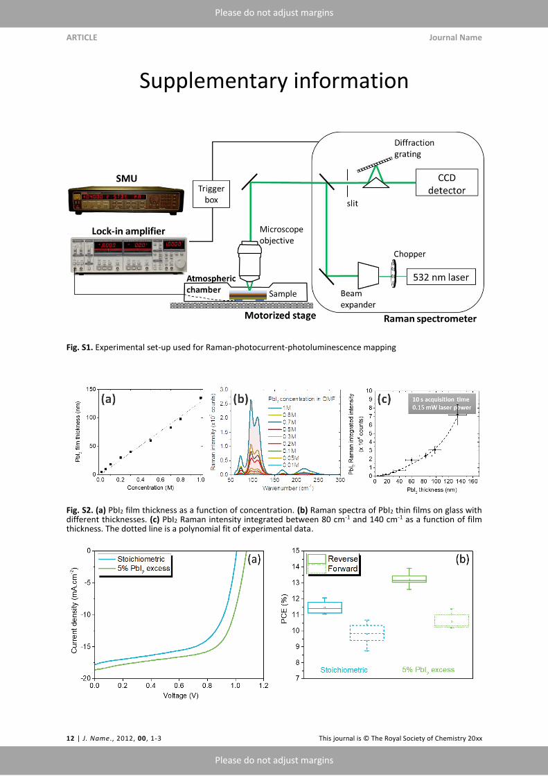
3 nm with an error margin of 20%27. To quantify the amount of
crystalline PbI2 present in the complete perovskite device stack, we
calibrated our Raman system by preparing PbI2 thin films having
various thicknesse. Raman spectra of PbI2 films measured with 0.15
mW laser power and 10 s acquisition time are shown in Fig. S2b. After
baseline subtraction, we observe a systematic decrease in intensity of
PbI2 peaks as the PbI2 concentration/thickness is decreased; a
property that allows us to determine the limit of detectability of PbI2
by Raman. The minimum detectable thickness by Raman is 18 ± 5 nm
(corresponding to 0.1 M PbI2 concentration). We then plot the PbI2
Raman intensity (integrated intensity between 80 cm-1 and 140 cm-1)
as a function of film thickness (Fig. S2c). This indicates a non-linear
dependence of the Raman intensity versus thickness which can be
used to estimate the PbI2 effective thickness within the layer stack and
obtain a PbI2 relative thickness map after laser irradiation, as shown in
Fig. 1f.
From this map, we measured a minimum PbI2 thickness of 25 ± 5 nm
after laser irradiation having a power of 1.5 mW and 10 s illumination
time (values below 25 ± 5 nm correspond to background noise). We
note that a 25 nm-thick PbI2 film would act as an insulating layer at the
interface with the HTL and would thus block charge transfer10. This
suggests that as soon as PbI2 is detected by Raman in the device
configuration, it is already too thick to be beneficial for device
performance, a result confirmed by the photocurrent map that shows
a decrease in photocurrent in all areas in which PbI2 was detected by
Raman spectroscopy. In contrast, in areas of high photocurrent (e.g.
for an irradiated spot created using a 1.5 mW laser for 1 s), the PbI2
Raman signal cannot be detected at these measurement settings,
indicating that the PbI2 effective thickness is less than 18 ± 5 nm. The
sensitivity of Raman to PbI2 could most likely be enhanced by using
higher laser power or longer acquisition times, however this
measurement condition would likely damage the perovskite film and
induce further formation of PbI2, as shown in our previous work23. The
maximum PbI2 effective thickness measured within the bright PbI2
halo is estimated to be around 80 nm. This demonstrates that Raman
spectroscopy is a non-destructive technique that can be used to
quantitatively determine the quantity and distribution of PbI2 formed
during photodegradation of perovskite devices, with this technique
having micrometer lateral resolution and relatively high sensitivity
down to an effective PbI2 thickness of approximately 20 nm. Raman
spectra of fresh PSCs with various excess of PbI2 incorporated directly
in the precursors solution were also measured (Fig. S4). The spectra
show typical weak and broad bands of CH3NH3PbI3 at 250 cm-1 and 110
cm-1, however no PbI2 signal is detected; a result that confirms that
PbI2 phase is present at concentrations that cannot be detected by
Raman using our experimental settings.
Improved optoelectronic properties of perovskite solar cells after
laser irradiation with reduced power
We have previously observed that laser irradiation at relatively high
power density can accelerate the photodegradation of perovskite
devices and generate PbI2 at a perovskite/NiOx interface. We now
investigate the effect of reduced laser irradiation on the local
ARTICLE Journal Name
6 | J. Name., 2012, 00, 1-3 This journal is © The Royal Society of Chemistry 20xx
Please do not adjust margins
Please do not adjust margins
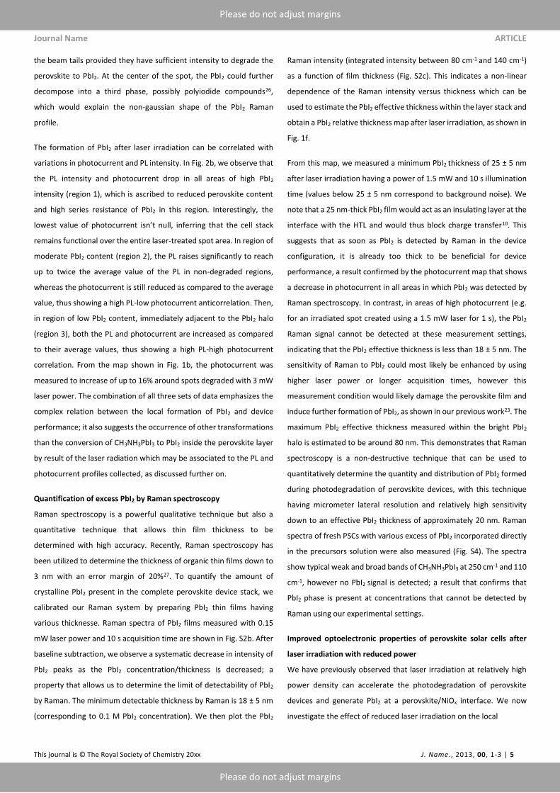
Fig. 3 Photo-electrical measurements of perovskite solar cell irradiated with laser power 0.3 mW for 120 s. (a) Photocurrent map on a 120 ´m x 120 ´m region.
(b) Photoluminescence intensity at ခ775 nm. (c) Stabilized photocurrent at short-circuit measured on irradiated (yellow) and non-irradiated (purple) regions.
photocurrent and photoluminescence behaviours in a PSC. To do this,
;ミ ;ヴヴ;┞ ラa ヶ┝ヶ ゲヮラデゲ ゲWヮ;ヴ;デWS H┞ ヲヰ ´マ ┘;ゲ キヴヴ;Sキ;デWS ┌ゲキミェ ; ノ;ゲWヴ
power of 0.3 mW for 120 s. As perovskites are known to be largely
inhomogeneous at the micrometer scale28, the same irradiation
conditions were applied to confirm that the observed laser-induced
effects are not due to specific localized microstructure or defects. In
Fig. 3a, a clear increase in photocurrent can be observed at regions in
which the perovskite device was irradiated, with an average
enhancement in photocurrent of 7% compared to non-irradiated
regions. The stabilized photocurrent at short-circuit shown in Fig. 3c
indicates the same enhancement in photocurrent from irradiated
regions, even after 180 s of illumination. This indicates that
optoelectronic/chemical changes in the perovskite device after
キヴヴ;Sキ;デキラミ ;ヴW ヮWヴマ;ミWミデ ;ミS Sラミげデ ヴWゲ┌ノデ aヴラマ デヴ;ミゲキWミデ マWIエ;ミキゲマゲ
such as ion migration. The PL intensity map at 775 nm (Fig. 3b)
indicates a slight increase in PL intensity from the irradiated regions.
Besides, in contrast to results shown in Fig. 1 (higher laser powers), no
halo surrounding irradiated regions is detected. Raman mapping did
not detect a PbI2 signal, from either the irradiated or non-irradiated
regions, a result that suggests that significant quantities of PbI2 (> 20
nm effective thickness) were not created under these specific
irradiation conditions.
Impact of laser irradiation on the microstructure of the perovskite
layer
As small quantities of PbI2 in a device structure are challenging to
probe by RS, scanning electron microscopy (SEM) and energy
dispersive spectroscopy (EDS) were used to gain further insights into
the perovskite microstructure and distribution of PbI2. Here,
CH3NH3PbI3 thin films were fabricated onto a glass/ITO/NiOx substrate
and exposed to laser irradiation in air. As the perovskite films were
directly exposed to air during the irradiation and were not covered by
PCBM/BCP/Ag top layers, reduced laser powers of 0.3 mW and 0.03
mW were used to obtain similar degradation levels as used in devices
degraded with 3 mW (strong irradiation) and 0.3 mW (mild
irradiation), respectively.
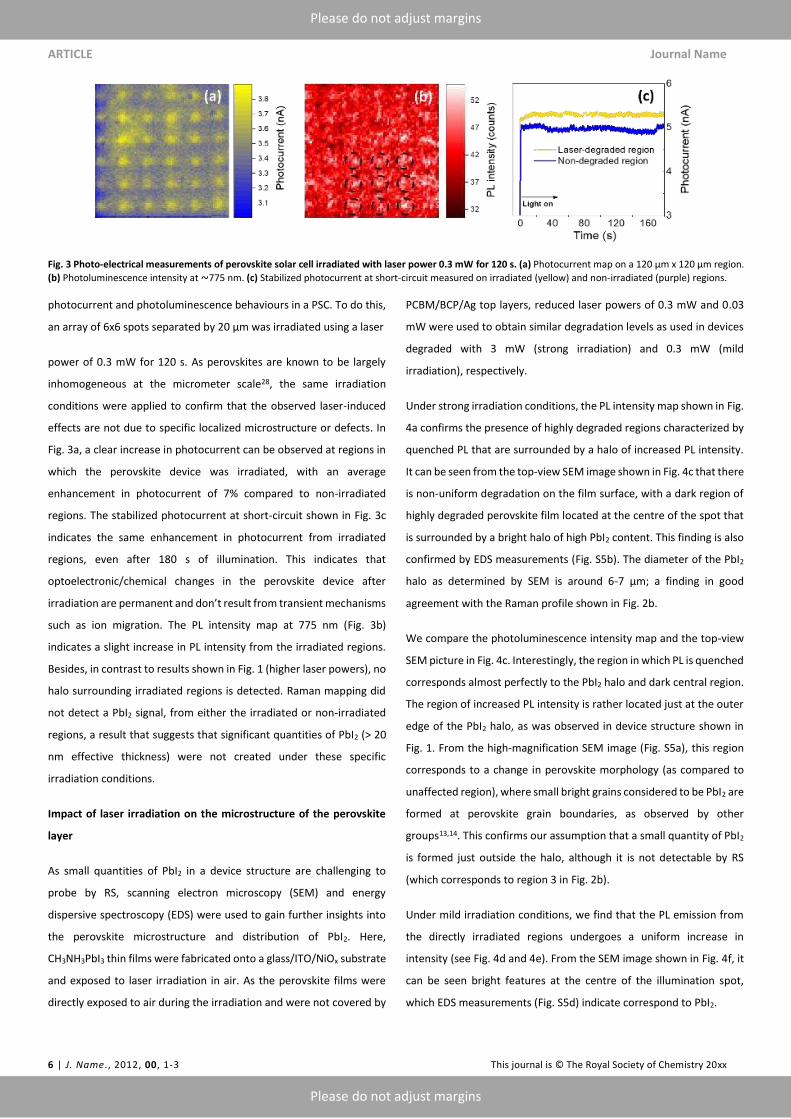
Under strong irradiation conditions, the PL intensity map shown in Fig.
4a confirms the presence of highly degraded regions characterized by
quenched PL that are surrounded by a halo of increased PL intensity.
It can be seen from the top-view SEM image shown in Fig. 4c that there
is non-uniform degradation on the film surface, with a dark region of
highly degraded perovskite film located at the centre of the spot that
is surrounded by a bright halo of high PbI2 content. This finding is also
confirmed by EDS measurements (Fig. S5b). The diameter of the PbI2
halo as determined by SEM is around 6-Α ´マき ; finding in good
agreement with the Raman profile shown in Fig. 2b.
We compare the photoluminescence intensity map and the top-view
SEM picture in Fig. 4c. Interestingly, the region in which PL is quenched
corresponds almost perfectly to the PbI2 halo and dark central region.
The region of increased PL intensity is rather located just at the outer
edge of the PbI2 halo, as was observed in device structure shown in
Fig. 1. From the high-magnification SEM image (Fig. S5a), this region
corresponds to a change in perovskite morphology (as compared to
unaffected region), where small bright grains considered to be PbI2 are
formed at perovskite grain boundaries, as observed by other
groups13,14. This confirms our assumption that a small quantity of PbI2
is formed just outside the halo, although it is not detectable by RS
(which corresponds to region 3 in Fig. 2b).
Under mild irradiation conditions, we find that the PL emission from
the directly irradiated regions undergoes a uniform increase in
intensity (see Fig. 4d and 4e). From the SEM image shown in Fig. 4f, it
can be seen bright features at the centre of the illumination spot,
which EDS measurements (Fig. S5d) indicate correspond to PbI2.
Journal Name ARTICLE
This journal is © The Royal Society of Chemistry 20xx J. Name., 2013, 00, 1-3 | 7
Please do not adjust margins
Please do not adjust margins
Fig. 4 Perovskite film microstructure after laser irradiation. (a) and (b) Photoluminescence intensity maps at 775 nm and (c) top-view SEM images of perovskite films on NiOx/ITO/glass substrates after laser degradation with 0.30 mW laser power for 120 s (equivalent of 3 mW for devices). (d) and (e) Photoluminescence intensity maps at 775 nm and (f) top-view SEM images of perovskite films on NiOx/ITO/glass substrates after laser degradation with 0.03 mW laser power for 120 s.
However, we also find that there is a significant carbon content (17.4
wt%) at the irradiated region, which is just slightly lower than that
found at non-irradiated regions (21 wt% in Fig. S5b and d). This
indicates that non-degraded perovskite material is still present
underneath the overlying PbI2 layer (at 10 kV, the e- penetration depth
of the primary electron beam is around 600 nm with 90% of the beam
energy dissipated in the top 200 nm thickness). This indicates that
under mild laser irradiation conditions, a thin PbI2 film forms at the
surface of the perovskite layer as a result of photodegradation. EDS
measurements indicate that this PbI2 film is very thin as unaffected
perovskite is still measured underneath, on the contrary to regions
having thick PbI2 film (Fig. S5b). This is also in good correlation with
our quantification of the PbI2 amount by RS showing that the PbI2
effective thickness is less than 20 nm when PbI2 peaks are not
distinguishable from background noise in the Raman spectra. Such
thin PbI2 film acts as a passivation layer for non-radiative defects on
top of the perovskite surface, as revealed by the PL enhancement
observed at irradiated spots in Fig. 4d. In the device structure, we also
believe that a thin PbI2 passivation layer can be formed at the interface
between the perovskite and NiOx HTL, which is sufficiently thin that it
cannot be detected by RS.
DISCUSSION
From these results, it is apparent that the formation of PbI2 that occurs
as a product of perovskite photodegradation has a significant effect
on PSCs performance, and the concentration of PbI2 generated within
the device stack determines its effect on the local photocurrent. In
scheme 1, we propose a mechanism of PbI2 passivation at the
perovskite/NiOx interface consistent with our observations in this
work. For strong laser illumination (3 mW), both hypothesis of iodide
redistribution or thermal degradation result in the formation of a thick
PbI2 halo, having a detrimental effect on the local photocurrent. Here,
a small amount of PbI2 is most likely located just outside the
degradation halo, although this cannot be detected by Raman. Indeed,
in Fig. S5a PbI2 clusters (identifiable as bright features) can be
observed that correlate with areas of high PL intensity and enhanced
photocurrent. Under mild irradiation conditions, a very thin layer of
PbI2 appears to form at the centre of the laser spot and also causes
similar effects (increased local PL intensity and photocurrent). Our
calibration using Raman spectroscopy indicates the effective thickness
of the PbI2 film to be less than 20 nm. It appears therefore that excess
PbI2 results in enhanced photocurrent when its effective thickness is
less than 20 nm, whether it is created using strong or mild laser
irradiation conditions.
The correlation between higher photoluminescence and higher
photocurrent in regions where a thin PbI2 layer is formed supports the
hypothesis that PbI2 acts as a passivation layer at the perovskite/NiOx
interface10. As discussed earlier, PbI2 is able to create a better
electronic coupling between the active layer and the extraction layer,
leading to reduced PL emission intensity as carriers will be extracted
ARTICLE Journal Name
8 | J. Name., 2012, 00, 1-3 This journal is © The Royal Society of Chemistry 20xx
Please do not adjust margins
Please do not adjust margins
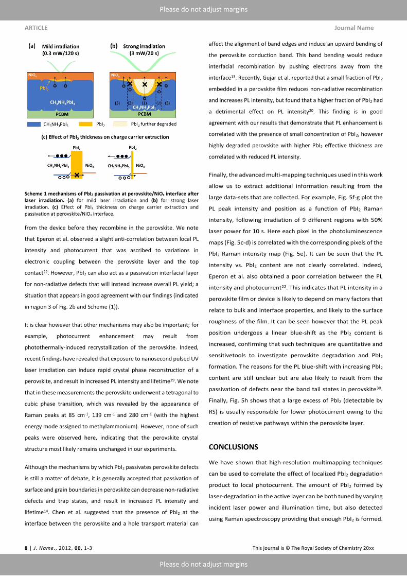
Scheme 1 mechanisms of PbI2 passivation at perovskite/NiOx interface after
laser irradiation. (a) for mild laser irradiation and (b) for strong laser irradiation. (c) Effect of PbI2 thickness on charge carrier extraction and passivation at perovskite/NiOx interface.
from the device before they recombine in the perovskite. We note
that Eperon et al. observed a slight anti-correlation between local PL
intensity and photocurrent that was ascribed to variations in
electronic coupling between the perovskite layer and the top
contact22. However, PbI2 can also act as a passivation interfacial layer
for non-radiative defects that will instead increase overall PL yield; a
situation that appears in good agreement with our findings (indicated
in region 3 of Fig. 2b and Scheme (1)).
It is clear however that other mechanisms may also be important; for
example, photocurrent enhancement may result from
photothermally-induced recrystallization of the perovskite. Indeed,
recent findings have revealed that exposure to nanosecond pulsed UV
laser irradiation can induce rapid crystal phase reconstruction of a
perovskite, and result in increased PL intensity and lifetime29. We note
that in these measurements the perovskite underwent a tetragonal to
cubic phase transition, which was revealed by the appearance of
Raman peaks at 85 cm-1, 139 cm-1 and 280 cm-1 (with the highest
energy mode assigned to methylammonium). However, none of such
peaks were observed here, indicating that the perovskite crystal
structure most likely remains unchanged in our experiments.
Although the mechanisms by which PbI2 passivates perovskite defects
is still a matter of debate, it is generally accepted that passivation of
surface and grain boundaries in perovskite can decrease non-radiative
defects and trap states, and result in increased PL intensity and
lifetime14. Chen et al. suggested that the presence of PbI2 at the
interface between the perovskite and a hole transport material can
affect the alignment of band edges and induce an upward bending of
the perovskite conduction band. This band bending would reduce
interfacial recombination by pushing electrons away from the
interface13. Recently, Gujar et al. reported that a small fraction of PbI2
embedded in a perovskite film reduces non-radiative recombination
and increases PL intensity, but found that a higher fraction of PbI2 had
a detrimental effect on PL intensity20. This finding is in good
agreement with our results that demonstrate that PL enhancement is
correlated with the presence of small concentration of PbI2, however
highly degraded perovskite with higher PbI2 effective thickness are
correlated with reduced PL intensity.
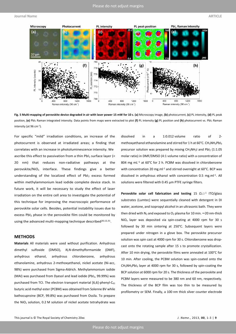
Finally, the advanced multi-mapping techniques used in this work
allow us to extract additional information resulting from the
large data-sets that are collected. For example, Fig. 5f-g plot the
PL peak intensity and position as a function of PbI2 Raman
intensity, following irradiation of 9 different regions with 50%
laser power for 10 s. Here each pixel in the photoluminescence
maps (Fig. 5c-d) is correlated with the corresponding pixels of the
PbI2 Raman intensity map (Fig. 5e). It can be seen that the PL
intensity vs. PbI2 content are not clearly correlated. Indeed,
Eperon et al. also obtained a poor correlation between the PL
intensity and photocurrent22. This indicates that PL intensity in a
perovskite film or device is likely to depend on many factors that
relate to bulk and interface properties, and likely to the surface
roughness of the film. It can be seen however that the PL peak
position undergoes a linear blue-shift as the PbI2 content is
increased, confirming that such techniques are quantitative and
sensitivetools to investigate perovskite degradation and PbI2
formation. The reasons for the PL blue-shift with increasing PbI2
content are still unclear but are also likely to result from the
passivation of defects near the band tail states in perovskite30.
Finally, Fig. 5h shows that a large excess of PbI2 (detectable by
RS) is usually responsible for lower photocurrent owing to the
creation of resistive pathways within the perovskite layer.
CONCLUSIONS
We have shown that high-resolution multimapping techniques
can be used to correlate the effect of localized PbI2 degradation
product to local photocurrent. The amount of PbI2 formed by
laser-degradation in the active layer can be both tuned by varying
incident laser power and illumination time, but also detected
using Raman spectroscopy providing that enough PbI2 is formed.
Journal Name ARTICLE
This journal is © The Royal Society of Chemistry 20xx J. Name., 2013, 00, 1-3 | 9
Please do not adjust margins
Please do not adjust margins
Fig. 5 Multi-mapping of perovskite device degraded in air with laser power 15 mW for 10 s. (a) Microscopy image, (b) photocurrent, (c) PL intensity, (d) PL peak
position, (e) PbI2 Raman integrated intensity. Data points from maps were extracted to plot (f) PL intensity (g) PL position and (h) photocurrent vs. PbI2 Raman
intensity (at 96 cm-1).
Fラヴ ゲヮWIキaキI さマキノSざ キヴヴ;Sキ;デキラミ IラミSキデキラミゲが ;ミ キミIヴW;ゲW ラa デエW
photocurrent is observed at irradiated areas; a finding that
correlates with an increase in photoluminescence intensity. We
ascribe this effect to passivation from a thin PbI2 surface layer (<
20 nm) that reduces non-radiative pathways at the
perovskite/NiOx interface. These findings give a better
understanding of the localized effect of PbI2 excess formed
within methylammonium lead iodide complete device stack. In
future work, it will be necessary to study the effect of laser
irradiation on the entire cell area to investigate the potential of
this technique for improving the macroscopic performance of
perovskite solar cells. Besides, potential instability issues due to
excess PbI2 phase in the perovskite film could be monitored by
using the advanced multi-mapping technique described20,12,31.
METHODS
Materials All materials were used without purification. Anhydrous
dimethyl sulfoxide (DMSO), N,N-dimethylformamide (DMF),
anhydrous ethanol, anhydrous chlorobenzene, anhydrous
ethanolamine, anhydrous 2-methoxyethanol, nickel acetate (Ni-acc,
98%) were purchased from Sigma-Aldrich. Methylammonium iodide
(MAI) was purchased from Dyesol and lead iodide (PbI2, 99.99%) was
purchased from TCI. The electron transport material [6,6]-phenyl-C61
butyric acid methyl ester (PCBM) was obtained from Solenne BV while
bathocuproine (BCP, 99.8%) was purchased from Ossila. To prepare
the NiOx solution, 0.2 M solution of nickel acetate tetrahydrate was
dissolved in a 1:0.012 volume ratio of 2-
methoxyethanol:ethanolamine and stirred for 1 h at 60°C. CH3NH3PbI3
precursor solution was prepared by mixing CH3NH3I and PbI2 (1:1.05
molar ratio) in DMF/DMSO (4:1 volume ratio) with a concentration of
804 mg mLЪヱ at 60°C for 2 h. PCBM was dissolved in chlorobenzene
with concentration 20 mg.ml-1 and stirred overnight at 60°C. BCP was
dissolved in anhydrous ethanol with concentration 0.5 mg.ml-1. All
ゲラノ┌デキラミゲ ┘WヴW aキノデWヴWS ┘キデエ ヰくヴヵ ´マ PTFE ゲ┞ヴキミェW aキノデWヴゲく
Perovskite solar cell fabrication and testing ヱヵ びく病-1 ITO/glass
substrates (Lumtec) were sequentially cleaned with detergent in DI
water, acetone, and isopropyl alcohol in an ultrasonic bath. They were
then dried with N2 and exposed to O2 plasma for 10 min. ခ20 nm-thick
NiOx layer was deposited via spin-coating at 4000 rpm for 30 s
followed by 30 min sintering at 250°C. Subsequent layers were
prepared under nitrogen in a glove box. The perovskite precursor
solution was spin cast at 4000 rpm for 30 s. Chlorobenzene was drop-
cast onto the rotating sample after 15 s to promote crystallization.
After 10 min drying, the perovskite films were annealed at 100°C for
10 min. After cooling, the PCBM solution was spin-coated onto the
CH3NH3PbI3 layer at 4000 rpm for 30 s, followed by spin-coating the
BCP solution at 6000 rpm for 20 s. The thickness of the perovskite and
PCBM layers were measured to be 380 nm and 60 nm, respectively.
The thickness of the BCP film was too thin to be measured by
profilometry or SEM. Finally, a 100 nm thick silver counter electrode
ARTICLE Journal Name
10 | J. Name., 2012, 00, 1-3 This journal is © The Royal Society of Chemistry 20xx
Please do not adjust margins
Please do not adjust margins
was evaporated at 10Ъヴ Torr using an Edwards 306 thermal
evaporator, forming devices with an active area of 0.15 cm2.
Crystalline PbI2 films were prepared on glass substrates by spin-
coating solutions of PbI2 in DMF with concentrations from 0.01 M to 1
M to adjust the film thickness, followed by annealing at 70°C for 10
min. Films thickness was measured by profilometry and tapping mode
atomic force microscopy (AFM).
Current densityにvoltage (JにV) characterization was performed using a
Keithley 2400 source-meter unit under 0.8 sun illumination using a
Newport 92193A-1000 solar simulator. Current-voltage sweeps were
performed from both VOC-to-JSC and vice versa at a rate of 0.1 V sЪヱ.
Photocurrent-photoluminescence-Raman mapping Multi-mapping
experiments were performed using a Renishaw Invia Raman system in
backscattering configuration, as shown in Fig. S1. The sample was
mounted in an electrical/environmental chamber (LTS420E, Linkam
Scientific Instrument) attached to a motorized stage (100 nm step
resolution). A laser excitation at 532 nm and a 50x long objective were
used (NA = 0.50, spot size ခヱ ´マぶく PエラデラI┌ヴヴWミデ ;ミS
photoluminescence maps were acquired simultaneously at laser
power of 30 nW (3000 mW.cm-2, 30 suns) and acquisition time of 0.2
s for each measurement spot to perform measurements without
affecting the perovskite layer. This was found to be the minimum
intensity required to measure the photocurrent with a good signal-to-
noise ratio.
The stage was translated in x and y directions to map the photocurrent
(short-circuit current) and PL spectra from each spot. To acquire the
photocurrent (also called LBIC for laser beam-induced current32), the
device electrodes were connected to a lock-in amplifier (Stanford
Research SR830) with the laser beam chopped at a frequency of 134
kHz. A source-meter unit (Keithley 236) was used to measure the
stabilized short-circuit current at specific regions of the perovskite
cells. Raman measurements were also performed using a laser power
of 0.15 mW and acquisition time of 10 s. All laser
degradations/irradiations were performed in air, whereas
photocurrent-PL-Raman mapping were performed under N2.
Electron microscopy
To avoid any damage due to electron beam, a FEI Helios NanoLab
G3 UC low voltage SEM was used to image CH3NH3PbI3 perovskite
thin films. All samples were imaged using a through-lens (TLD)
detector at a working distance of ခ4.1 mm with a beam current
of 13 pA and an accelerating voltage of 1 kV. Compositional
analysis was performed using energy dispersive X-ray
spectroscopy (EDX) using the FEI Helios NanoLab equipped with
an Oxford EDX detector and the data were collected with an
accelerating voltage of 10 keV and a beam current of 25 pA.
ASSOCIATED CONTENT
Experimental set-up used for Raman-photocurrent-
photoluminescence mapping, Raman spectra of PbI2 thin films on
glass with different thicknesses, Raman spectra of MAPbI3 films
on ITO/glass substrates prepared with different amounts of PbI2
excess, high and low magnification SEM top-view images of
irradiated perovskite films.
ACKNOWLEDGMENTS
The authors acknowledge funding from the EPSRC (grant no
EP/M025020/1), Welsh Assembly Government funded SZr Cymru
Solar Project. V.K and C.R. would like to thank EPSRC for financial
support under projects EP/N008065/1, EP/M025020/1 and
EP/L017563/1 and for the use of the University of Sheffield
electron microscopy facilities.
REFERENCES
1 S. De Wolf, J. Holovsky, S. J. Moon, P. Loper, B. Niesen, M.
Ledinsky, F. J. Haug, J. H. Yum and C. Ballif, J. Phys. Chem.
Lett., 2014, 5, 1035に1039.
2 S. D. Stranks, S. D. Stranks, G. E. Eperon, G. Grancini, C.
Menelaou, M. J. P. Alcocer, T. Leijtens, L. M. Herz, A.
Petrozza and H. J. Snaith, Science, 2014, 341, 341に345.
3 K. X. Steirer, P. Schulz, G. Teeter, V. Stevanovic, M. Yang, K.
Zhu and J. J. Berry, ACS Energy Lett., 2016, 1, 360に366.
4 J.-P. Correa-Baena, A. Abate, M. Saliba, W. Tress, T. Jesper
Jacobsson, M. Grätzel and A. Hagfeldt, Energy Environ. Sci.,
2017, 10, 710に727.
5 W. E. I. Sha, X. Ren, L. Chen and W. C. H. Choy, Appl. Phys.
Lett., 2015, 106, 221104.
6 T. A. Berhe, W.-N. Su, C.-H. Chen, C.-J. Pan, J.-H. Cheng, H.-
M. Chen, M.-C. Tsai, L.-Y. Chen, A. A. Dubale and B.-J.
Hwang, Energy Environ. Sci., 2016, 9, Advance Article.
7 S. Wang, W. Dong, X. Fang, Q. Zhang, S. Zhou, Z. Deng, R.
Tao, J. Shao, R. Xia, C. Song, L. Hu and J. Zhu, Nanoscale,
2016, 8, 6600に6608.
8 Y. C. Kim, N. J. Jeon, J. H. Noh, W. S. Yang, J. Seo, J. S. Yun, A.
Ho-baillie, S. Huang, M. A. Green and J. Seidel, Adv. Energy
Mater., 2016, 6, 1502104.
9 C. Roldán-Carmona, P. Gratia, I. Zimmermann, G. Grancini,
P. Gao, M. Graetzel and M. K. Nazeeruddin, Energy Environ.
Journal Name ARTICLE
This journal is © The Royal Society of Chemistry 20xx J. Name., 2013, 00, 1-3 | 11
Please do not adjust margins
Please do not adjust margins
Sci., 2015, 8, 3550に3556.
10 T. J. Jacobsson, J. P. Correa-Baena, E. Halvani Anaraki, B.
Philippe, S. D. Stranks, M. E. F. Bouduban, W. Tress, K.
Schenk, J. Teuscher, J. E. Moser, H. Rensmo and A. Hagfeldt,
J. Am. Chem. Soc., 2016, 138, 10331に10343.
11 D. H. Cao, C. C. Stoumpos, C. D. Malliakas, M. J. Katz, O. K.
Farha, J. T. Hupp and M. G. Kanatzidis, APL Mater., 2014, 2,
1に8.
12 F. Liu, Q. Dラミェが Mく Kく Wラミェが Aく Bく Dテ┌ヴキジキJが Aく Nェが Zく RWミが Qく Shen, C. Surya, W. K. Chan, J. Wang, A. M. C. Ng, C. Liao, H.
Li, K. Shih, C. Wei, H. Su and J. Dai, Adv. Energy Mater., 2016,
6, 1に9.
13 Q. Chen, H. Zhou, T. Bin Song, S. Luo, Z. Hong, H. S. Duan, L.
Dou, Y. Liu and Y. Yang, Nano Lett., 2014, 14, 4158に4163.
14 S. Chen, X. Wen, J. S. Yun, S. Huang, M. Green, N. J. Jeon, W.
S. Yang, J. H. Noh, J. Seo, S. Il Seok and A. Ho-Baillie, ACS
Appl. Mater. Interfaces, 2017, 9, 6072に6078.
15 M. Saliba, T. Matsui, J.-Y. Seo, K. Domanski, J.-P. Correa-
Baena, M. K. Nazeeruddin, S. M. Zakeeruddin, W. Tress, A.
Abate, A. Hagfeldt and M. Grätzel, Energy Environ. Sci.,
2016, 9, 1989に1997.
16 Q. Chen, H. Zhou, Z. Hong, S. Luo, H. Duan, H. Wang, Y. Liu,
G. Li and Y. Yang, J. Am. Chem. Soc., 2014, 136, 622に625.
17 Z. Xiao, C. Bi, Y. Shao, Q. Dong, Q. Wang, Y. Yuan, C. Wang, Y.
Gao and J. Huang, Energy Environ. Sci., 2014, 7, 2619に2623.
18 D. Zhao, M. Sexton, H. Y. Park, G. Baure, J. C. Nino and F. So,
Adv. Energy Mater., 2015, 5, 1に5.
19 T. Du, C. Burgess, J. Kim, J. Durrant, J. Zhang and M.
McLachlan, Sustain. Energy Fuels, 2017, 119に126.
20 T. P. Gujar, T. Unger, A. Schönleber, M. Fried, F. Panzer, S.
van Smaalen, A. Köhler and M. Thelakkat, Phys. Chem.
Chem. Phys., 2017, 85, 605に614.
21 S. Y. Leblebici, L. Leppert, Y. Li, S. E. Reyes-Lillo, S.
Wickenburg, E. Wong, J. Lee, M. Melli, D. Ziegler, D. K.
Angell, D. F. Ogletree, P. D. Ashby, F. M. Toma, J. B. Neaton,
I. D. Sharp and A. Weber-Bargioni, Nat. Energy, 2016, 1, 1に7.
22 G. E. Eperon, D. Moerman and D. S. Ginger, ACS Nano, 2016,
10, 10258に10266.
23 K. E. A. Hooper, H. K. H. Lee, M. J. Newman, S. Meroni, J.
Baker, T. M. Watson and W. C. Tsoi, Phys. Chem. Chem.
Phys., 2017, 19, 5246に5253.
24 F. Jiang, Y. Rong, H. Liu, T. Liu, L. Mao and W. Meng, Adv.
Funct. Mater., 2016, 26, 8119に8127.
25 D. W. DeQuilettes, W. Zhang, V. M. Burlakov, D. J. Graham,
Tく LWキテデWミゲが Aく OゲエWヴラ┗が Vく B┌ノラ┗キJが Hく Jく “ミ;キデエが Dく “く GキミェWヴ and S. D. Stranks, Nat. Commun., ,
DOI:10.1038/ncomms11683.
26 P. Pistor, A. Ruiz, A. Cabot and V. Izquierdo-Roca, Sci. Rep.,
2016, 6, 35973.
27 B. M. Liszka, A. T. M. Lenferink, G. J. Witkamp and C. Otto, J.
Raman Spectrosc., 2015, 46, 1230に1234.
28 G. El-Hajje, C. Momblona, L. Gil-Escrig, J. Ávila, T. Guillemot,
J.-F. Guillemoles, M. Sessolo, H. J. Bolink and L. Lombez,
Energy Environ. Sci., 2016, 9, 2286に2294.
29 T. Abraha, J. Cheng, W.-N. Su, C.-J. Pan, M. Tsai, H.-M. Chen,
Z. Yang, H. Tan, C.-H. Chen, M.-H. Yeh, A. G. Tamirat, H.-F.
Huang, L.-Y. Chen, J.-F. Lee, Y.-F. Liao, E. H. Sargent, H. Dai
and B. J. Hwang, J. Mater. Chem. A, 2017, 5, 21002に21015.
30 Y. Shao, Z. Xiao, C. Bi, Y. Yuan and J. Huang, Nat. Commun.,
2014, 5, 1に7.
31 M. L. Petrus, Y. Hu, D. Moia, P. Calado, A. M. A. Leguy, P. R.
F. Barnes and P. Docampo, ChemSusChem, 2016, 9, 2699に2707.
32 Z. Song, A. Abate, S. C. Watthage, G. K. Liyanage, A. B.
Phillips, U. Steiner, M. Graetzel and M. J. Heben, Adv. Energy
Mater., 2016, 6, 1に7.
ARTICLE Journal Name
12 | J. Name., 2012, 00, 1-3 This journal is © The Royal Society of Chemistry 20xx
Please do not adjust margins
Please do not adjust margins
Supplementary information
Fig. S1. Experimental set-up used for Raman-photocurrent-photoluminescence mapping
Fig. S2. (a) PbI2 film thickness as a function of concentration. (b) Raman spectra of PbI2 thin films on glass with different thicknesses. (c) PbI2 Raman intensity integrated between 80 cm-1 and 140 cm-1 as a function of film thickness. The dotted line is a polynomial fit of experimental data.
Journal Name ARTICLE
This journal is © The Royal Society of Chemistry 20xx J. Name., 2013, 00, 1-3 | 13
Please do not adjust margins
Please do not adjust margins
Fig. S3. (a) Typical J-V curves of perovskite solar cells with structure glass/ITO/NiOx/CH3NH3PbI3/PCBM/BCP/Ag
using stoichiometric or 5% PbI2 excess perovskite solution. (b) statistical power conversion efficiency data for
10 different devices having stoichiometric or 5% PbI2 excess perovskite.
Fig. S4. Raman spectra of MAPbI3 films on ITO/glass substrates prepared with different amounts of PbI2 excess. Each spectrum is an average of 200 data points measured using laser power of 0.15 mW for 10 s.
Fig. S5. high and low magnification SEM top-view images of perovskite films degraded with (a-b) 0.03 mW laser power for 120 s and (c-d) 0.3 mW laser power for 120 s in air, with corresponding Energy Dispersive Spectroscopy (EDS) measurements taken at various locations along the degraded spot (b and d).
50 100 150 200 250 300 350 400200
250
300
350
400
Ram
an in
tens
ity (
coun
ts)
Wavenumber (cm-1)
Stoichiometric 5% PbI
2 excess
10% PbI2 excess