logic circuits ii ece 2411 thursday 4:45pm-7:20pm 2016/ece2411/lecture2.pdf · external or gate...
TRANSCRIPT

Logic Circuits II ECE 2411
Thursday 4:45pm-7:20pm
Lecture 2

Chapter 4 Review

4.2 Combinational Circuits
• Combinational circuits consist of an interconnect of logic gates, configured to perform a given function
– For n inputs, there are 2n possible combinations
• Each output function is expressed in terms of the n inputs

4.3 Analysis Procedure
• The diagram of a combinational circuit has logic gates with no feedback paths or memory elements
– A feedback path is a connection from the output of gate to the input of a second gate whose output forms part of the input to the first gate

4.3 Analysis Procedure T2 = ABC
T1 = A + B +C
F2 = AB + AC + BC
T3 = F’2T1
F1 = T3 + T2
F1 = T3 + T2 = F’2T1 + ABC F1 = (AB + AC + BC)’(A + B + C) + ABC F1 = (A’ + B’)(A’ + C’)(B’ + C’)(A + B + C) + ABC F1 = (A’ B’C’)(AB’ + AC’ BC’ B’C) + ABC F1 = A’BC’ + A’B’C + AB’C’ ABC

4.3 Analysis Procedure
1

Code Conversion Example
• BCD to Excess-3 Code Conversion
• Excess-3 code
– Add three to value

BCD to Excess-3
BCD is valid for 0 – 9 so values above that are don’t cares

BCD to Excess-3
Recall distributive postulate: BC + BD = B(C+ D) x = B’C + B’D + BC’D’ = B’(C + D) + BC’D’ = B’(C + D) + B(C + D)’ y = CD + C’D’ = CD + (C + D)’ z = D’

• Half Adder
– Adds two single binary digits (A, B) and has two outputs, sum and carry (S, C)

• Full Adder – Adds three single binary digits (A, B, Cin) and has two outputs, sum and
carry (S, Cout) • Binary Adder (cont.):
– The K-Map for S looks like the familiar even pattern for an XOR:
S = xy’z’ + x’yz’ + xyz + x’y’z
= z’(xy’ + x’y) + z(xy + x’y’)
= z’(xy’ + x’y) + z(xy’ + x’y)’
Recall (x’)’ = x
= z’(xy’ + x’y) + z((xy + x’y’)’)’
= z’(xy’ + x’y) + z((xy)’(x’y’)’) DeMorgan’s
= z’(xy’ + x’y) + z((x’ + y’)(x + y))’ DeMorgan’s
= z’(xy’ + x’y) + z(xx’ + xy’ + x’y + yy’)’
= z’(xy’ + x’y) + z(xy’ + x’y)’ Postulate 5b
= z ⊕ (x ⊕ y)
– Similarly for C:
C = xy + xz + yz
= z(x + y) + xy
= z(x’y + y’x) + xy

Carry Look Ahead • Daisy Chaining full adders results in long path for
carry – Ripple carry value dependent on all previous carries. – Charles Babbage ( 1791 – 1871) recognized carry delay
issue and devised anticipating carriage mechanisms for his devices.
– First patent filed in 1957 by IBM

Carry Look Ahead • Define two new binary variables:
Pi = Ai + Bi (Carry Propagate – Determines if a carry propagates)
Gi = AiBi (Carry Generate – produces carry when A = B = 1)
• The output sum and carry can be expressed as
Si = Pi + Ci
Ci+1 = Gi + PiCi
• Carry output Boolean functions: C0 = input carry
C1 = G0 + P0C0

Carry Look Ahead (cont.)
• Four bit Adder Carry Output Boolean functions: C0 = input carry
C1 = G0 + P0C0
C2 = G1 + P1C1 = G1 + P1 (G0 + P0G0) = G1 + P1G0 + P1P0C0
C3 = G2 + P2C2 = G2 + P2G1 + P2P1G0 = P2P1P0C0
C1
C0
C1
P1
P0
G0
G1
+ P0C0
P1C1
+

Carry Look Ahead (cont.) • Four bit Adder Carry Output Boolean functions:
C0 = input carry
C1 = G0 + P0C0
C2 = G1 + P1C1 = G1 + P1 (G0 + P0G0) = G1 + P1G0 + P1P0C0
C3 = G2 + P2C2 = G2 + P2G1 + P2P1G0 = P2P1P0C0

4.7 Binary Multiplier • The multiplicand is multiplied by each bit of
the multiplier, starting with the LSB
• Each such multiplication forms a partial product
• The final product is obtained from the sum of the partial products – The multiplication of
Ai and Bi produce a 1 if both are 1;
otherwise it produces a 0 (AND operation)

4.7 Binary Multiplier
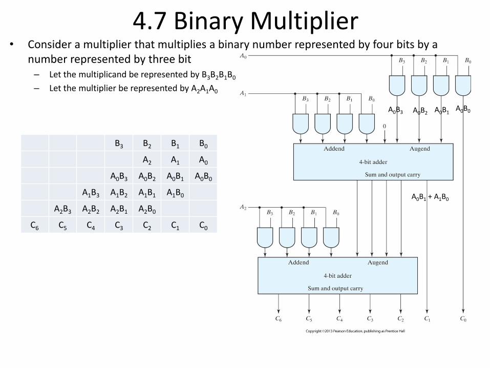
4.7 Binary Multiplier • Consider a multiplier that multiplies a binary number represented by four bits by a
number represented by three bit – Let the multiplicand be represented by B3B2B1B0
– Let the multiplier be represented by A2A1A0
B3 B2 B1 B0
A2 A1 A0
A0B3 A0B2 A0B1 A0B0
A1B3 A1B2 A1B1 A1B0
A2B3 A2B2 A2B1 A2B0
C6 C5 C4 C3 C2 C1 C0
A0B0 A0B1 A0B2 A0B3
A0B1 + A1B0

4.9 Decoders • Consider the truth table for a three-to-eight
line decoder:
– Each output represents one of the minterms of the three inputs

Decoders • Decode n input lines to 2n output lines
– May have fewer output if unused combinations
Minterms

Decoders
• Knowing that a 3 to 8 decoder provides all the Minterms, we can construct other functions such as a full adder:
S(x, y, z) = (1, 2, 4, 7)
C(x, y, z) = (3, 5, 6, 7)

Encoders • Encodes 2n input lines to n output lines
x = D4 + D5 + D6 + D7
y = D2 + D3 + D6 + D7
z = D1 + D3 + D5 + D7
• The 8 to 3 encoder can be implemented with three 4 input OR gates

4.11 Multiplexers • A multiplexer is a combinational circuit that
routes binary information from one of many inputs to a single output based on the select value – Acts an electronic switch
• (Single Pole, Double Throw) – Requires one select line
• Single Throw, Four Throw – Requires two select lines
– Block diagram shown as wedge shaped symbol, visually suggesting how multiple inputs are directed to a single output
– Often labeled “MUX”
Similar to the black three terminal switch in your kit

4.11 Multiplexers
Two-to-one line mux
Four-to-one line mux

4.11 Multiplexers
• Boolean Function Implementation
– Section 4.9 showed that a decoder can be used to implement Boolean functions by adding an external OR gate
– Examination of a multiplexer shows that it is essentially a decoder with an internal OR gate
– The minterms of a function are generated using the selection inputs of a mux with the individual minterms selected by the data inputs
– Thus a n variable Boolean function can be implemented with a n – 1 selection mux

4.11 Multiplexers • Consider:
F(x, y, z) = Σ(1, 2, 6, 7)
– This function can be implemented with a four-to-one line mux
• Apply:
x to S1
y to S0
• The data input values are determined from the function truth table

4.11 Multiplexers • Consider:
F(A, B, C, D) = Σ(1, 3, 4, 11, 12, 13, 14, 15)
– This function can be implemented with a four-to-one line mux
• Apply:
A to S2, B to S1, C to S0, D/D’ (and 1/0) to inputs

Three State Gates
• The gate has three states:
– Two states are signal equivalent to logic 1/0 as with conventional gate
– Third state
• No logic significance
• Electrically disconnected
• Output not affected by input

Three State Gates
• Three state gates can be used to construct multiplexers
Note: Y will always be driven by one of the tri-state gates in above examples. If application differs where Y could float, must use keeper cell

4.12 HDL Models Of Comb. Circuits
• The logic of a module can be described in any one or combination of the following modeling styles:
– Gate level: Uses instantiations of predefined and user defined primitive gates
– Dataflow: Uses continuous assignment statements with the keywords wire/assign
– Behavioral: Uses procedural assignment statements with the keyword always

4.12 HDL Models Of Comb. Circuits
• Gate Level Modeling – A circuit is specified by its logic gates and
interconnects • Four values assigned to output(s):
– Logic values: 0, 1
– Unknown: x
» Assigned when the logic value is ambiguous
• Flip-Flop prior to reset or data clocked in
• Bus contention: two or more drivers on net
– Hi-Impedance: z
» Assigned when nothing driving net
• Tri-state
• Wire inadvertently left unconnected

4.12 HDL Models Of Comb. Circuits • Dataflow Modeling:
– Bitwise operators perform a bit wise operation on two operands. • They take each bit in one operand and perform the operation with the
corresponding bit in the other operand. • If one operand is shorter than the other, it will be extended on the left side
with zeroes to match the length of the longer operand. – For a logical operation, a vector is tested for equality to 0. If it is, then its Boolean
value is defined as "false", otherwise "true" • Logical operator evaluation stops as soon as result is known • Expressions connected by && and || are evaluated from left to right • The result is a scalar value:
– False if relation is 0 – True if relation is 1 – Unknown (x) if any of the operands has x
– If the operands are scalar, the bitwise and logical will be identical – Be careful with bitwise versus logical operators:
~(1010) = 01010 but !(1010) = 0 – Reduction bitwise AND useful to check if value is all 1s:
&(1010) = 0, &(1111) = 1 – Reduction bitwise OR useful to check if value is all 0s:
|(1010) = 1, |(0000) = 0

Hardware Description Language • Boolean Expressions
– Verilog operators

Operator Precedence • Binary Operator Precedence
(A + B)/C is not the same as A + B/C
a & &b is not the same as a && b
correct syntax and required by LRM: a & (&b)
a | |b is not the same as a || b
correct syntax and required by LRM: a | (|b)

4.12 HDL Models Of Comb. Circuits module operands();
reg [3:0] A = 4'b1010; reg [3:0] B = 4'b1111; reg [3:0] C = 4'b0000; reg [3:0] D = 4'b0101;
initial begin
$display("~A = %4b", ~A); $display("!A = %4b", !A);
$display("&A = %4b", &A); $display("A & B = %4b", A&B); $display("A && B = %4b", A&&B); $display("A * B = %4b", A*B); $display("A | B = %4b", A|B); $display("A || B = %4b", A||B); $display("A + B = %4b", A+B);
$display("A & C = %4b", A&C); $display("A && C = %4b", A&&C); $display("A * C = %4b", A*C); $display("A | C = %4b", A|C); $display("A || C = %4b", A||C); $display("A + C = %4b", A+C);
end endmodule
For a logical operation, a vector is tested for equality to 0. If it is, then its Boolean value is defined as "false", otherwise "true"

Combinational Logic • Full Adder
module fullAdder ( output S, C, input wire x, y, z ); wire S0, C0, C1;
halfAdder ha0( .x(x), .y(y), .S(S0), .C(C0) ); halfAdder ha1( .x(S0), .y(z), .S(S), .C(C1) ); or (C, C0, C1); endmodule
// Half Adder module halfAdder ( output wire S, C, input x, y ); assign S = x ^ y; assign C = x && y; endmodule
// Dataflow coding module full_adder (Sum, Cout, A, B, Cin); input A, B, Cin; output Sum, Cout;
wire Sum, Cout;
assign Sum = Cin ^ (A ^ B); assign Cout = Cin * (A ^ B) + A*B; endmodule
& or

4.12 HDL Models Of Comb. Circuits
// Dataflow description of four-bit comparator module mag_compare ( output A_lt_B, A_eq_B, A_gt_B, input [3:0] A, B ); assign A_lt_B = (A<B); assign A_GT_B = (A > B); assign A_eq_B = (A == B); endmodule

4.12 HDL Models Of Comb. Circuits
• Conditional Operator:
– The conditional operator take three operands:
• condition ? true_expression : false_expression;
• The condition is evaluated – If the result is logic 1, the true_expression is evaluated and
used to assign a value to the left hand side of the equation
– If the result is logic 0, the false_expression is evaluated and used to assign a value to the left hand side of the equation
// Dataflow description of // two-to-one multiplexer module mux_2x1_df ( output m_out, input A, B, select ); assign m_out = select ? A : B; endmodule
Conditional operator can be used for tri-state buffer modeling. assign data_out = (enable) ? data_reg : 8'bz; Conditional operator can be nested assign out = sel[1] ? (sel[0] ? In3: in2) : (sel[0] ? In1 : in0);

4.12 HDL Models Of Comb. Circuits • Behavioral Modeling
– Behavioral descriptions use the keyword always, followed by optional event control expression and a list of procedural assignment statements
• The event control expression specifies when the statements will execute
• The target output of a procedural assignment statement must of the reg type
// Behavioral description of two-to-one multiplexer module mux_2x1_beh ( output reg m_out, input A, B, select ); always @(A or B or select) if(select) m_out = A; else m_out = B; endmodule
case statements
• default case: – An optional case to indicate what actions to perform if
none of the defined case items match the case expression – Good coding style to place the default last, though not
required by the Verilog LRM – If a case statement does not include a case default and if it
is not possible to find a binary case expression that matches any of the defined case items, the case statement is not "full." • Verilog does not require case statements to be “full” • If case statement not “full” and no default case, latch inferred
– Generates ELAB-311 Warning (DEFAULT branch of CASE statement cannot be reached.) during synthesis if case statement fully defined

case/casex/casez statement
// Example 1 reg a; case (a) 1'b0 : statement1; // Executes if variable ‘a’ is 1’b0 1'b1 : statement2; // Executes if variable ‘a’ is 1’b1 1'bx : statement3; // Executes if variable ‘a’ is 1’bx 1'bz : statement4; // Executes if variable ‘a’ is 1’bz or 1’b? endcase
// Example 3 // casex treats x, z, and ? as don’t care values // Per C. Cummings, don’t use casex for synthesizable code reg a; casex (a) 1'b0 : statement1; // Executes if variable ‘a’ is 1’b0 or 1’bz or 1’bx or 1’b? 1'b1 : statement2; // Executes if variable ‘a’ is 1’b1 1'bx : statement3; // Never executes 1'bz : statement4; // Never executes endcase
// Example 2 // casez treats z and ? as don’t care values reg a; casez (a) 1'b0 : statement1; // Executes if variable ‘a’ is 1’b0 or 1’bz or 1’b? 1'b1 : statement2; // Executes if variable ‘a’ is 1’b1 1'bx : statement3; // Executes if variable ‘a’ is 1’bx 1'bz : statement4; // Never executes endcase
• The case statement can appear only within structured procedures, i.e. always, initial, function or task
• Unlike other high level languages, the Verilog case statement includes implied break statements
• Verilog case item statements must be enclosed between the keywords "begin" and "end" if more than one statement is to be executed for a selected case item

4.12 HDL Models Of Comb. Circuits
// Behavioral description of four-to-one multiplexer module mux_4x1_beh ( output reg m_out, input in_0, in_1, in_2, in_3, input [1:0] select ); always @(in_0, in_1, in_2, in_3, select) case(select) 1’d0: m_out = in_0; 1’d1: m_out = in_1; 1’d2: m_out = in_2; 1’d3: m_out = in_3; endcase endmodule

Verilog Module Parameters • Allows instantiating module to pass and
redefine parameters into instantiated module `timescale 1ns/10ps module parameter_tb(); reg in = 0; wire u1_out, u2_out, u3_out; my_module u1 (in, u1_out); my_module #(8) u2 (in, u2_out); my_module #(.clk_dly(16)) u3 (in, u3_out); always begin #9 in <= !in; end endmodule module my_module (in, out); input in; output out; parameter clk_dly = 4; assign #clk_dly out = in; endmodule

4.12 HDL Models Of Comb. Circuits • Writing a Simple Test Bench:
– repeat(x) • Repeats x times the statements to “;”
– $display”<format>”, exp1, exp2, …); format indication:
%b %B binary %c %C character (low 8 bits) %d %D decimal %0d for minimum width field %e %E E format floating point %15.7E %f %F F format floating point %9.7F %g %G G general format floating point %h %H hexadecimal %l %L library binding information %m %M hierarchical name, no expression %o %O octal %s %S string, 8 bits per character, 2´h00 does not print %t %T simulation time, expression is $time %u %U unformatted two value data 0 and 1 %v %V net signal strength %z %Z unformatted four value data 0, 1, x, z
escape sequences, quoted characters in strings: n newline \t tab \\ backslash \" quote \ddd octal %% percent

Simple Testbench • Declare module without portlist
• initial statement executed only once when simulation starts – Statements within initial blocks execute in order
• always statement executes continuously – May or may not have sensitivity list
initial begin data = 0; reset = 0; #10 data = 8’hff; repeat(10) @(posedge clk); reset = 1; … end
always begin #5 clk = ~clk; end always @(poedge clk) begin … end
module simple_tb(); // or module simple_tb; … endmodule

Simple Testbench
• The $display statement is used to display the value of a variable in user specified formats – $display(“foo in hex: %h, dec: %d, bin: %b", foo, foo, foo);
• $monitor continuously monitors the values of the variables or signals in the parameter list and displays all values whenever any one changes
– Can switch on/off with $monitoron/$monitoroff

Simple Testbench
• $write – same as display but w/o new line return
• $time – displays the simulation time
• $finish – terminates the simulation

Verilog reg • “wire” is combinational and evaluates continuously • “reg” is sequential and evaluates on event
– Initial value of “x”* • Can specify initial value upon declaration
reg [7:0] foo = 8’hff; // Used with FPGAs
• Can be a value of “1”, “0”, or “x”;
– Note: for case statement, declare output as reg
* Simulators will initialize value to “x”, actual FPGAs initialize to “0” if not specified. When simulating for FPGAs, always specify upon declaration so simulations better match actual.
reg [7:0] foo_async; …. // Asynchronous Reset always @(posedge clk or posedge reset) if(reset) foo_async <= 8’hff; else foo_async <= foo_async + 1’b1;
reg [7:0] foo_sync; …. // Synchronous Reset (use with FPGAs) always @(posedge clk) if(reset) foo_sync <= 8’hff; else foo_sync <= foo_sync + 1’b1;

Verilog System Tasks $write // same as $display except no automatic insertion of newline $strobe // same as $display except waits until all events finished $monitor // same as $display except only displays if an expression changes $monitoron // only one $monitor may be active at ant time, $monitoroff // turn current $monitor off $displayb // same as $display using binary as default format $writeb // same as $write using binary as default format $strobeb // same as $strobe using binary as default format $monitorb // same as $monitor using binary as default format $displayo // same as $display using octal as default format $writeo // same as $write using octal as default format $strobeo // same as $strobe using octal as default format $monitoro // same as $monitor using octal as default format $displayh // same as $display using hexadecimal as default format $writeh // same as $write using hexadecimal as default format $strobeh // same as $strobe using hexadecimal as default format $monitorh // same as $monitor using hexadecimal as default format

Homework
• 4.7 a, b
• 4.14
• 4.35 a, b
• 4.39
• 4.43