lonworks twisted pair control module user's guide · lonworks twisted pair control module...
TRANSCRIPT
LONWORKS® Twisted PairControl Module User’s Guide
078-0015-01F

Echelon, LONWORKS, LONMARK, NodeBuilder, LonTalk, Neuron, 3120, 3150, ShortStack, LonMaker, and the Echelon logo are trademarks of Echelon Corporation registered in the United States and other countries.
Other brand and product names are trademarks or registered trademarks of their respective holders.
Smart Transceivers, Neuron Chips, and other OEM Products were not designed for use in equipment or systems, which involve danger to human health or safety, or a risk of property damage and Echelon assumes no responsibility or liability for use of the Smart Transceivers or Neuron Chips in such applications.
Parts manufactured by vendors other than Echelon and referenced in this document have been described for illustrative purposes only, and may not have been tested by Echelon. It is the responsibility of the customer to determine the suitability of these parts for each application.
ECHELON MAKES AND YOU RECEIVE NO WARRANTIES OR CONDITIONS, EXPRESS, IMPLIED, STATUTORY OR IN ANY COMMUNICATION WITH YOU, AND ECHELON SPECIFICALLY DISCLAIMS ANY IMPLIED WARRANTY OF MERCHANTABILITY OR FITNESS FOR A PARTICULAR PURPOSE.
No part of this publication may be reproduced, stored in a retrieval system, or transmitted, in any form or by any means, electronic, mechanical, photocopying, recording, or otherwise, without the prior written permission of Echelon Corporation.
Printed in the United States of America. Copyright © 1992, 2011 Echelon Corporation.
Echelon Corporation www.echelon.com
LonWorks Twisted Pair Control Module User's Guide iii
Welcome Echelon’s LONWORKS® Twisted Pair Control Modules contain the core elements for device designs using LONWORKS technology. The core elements of a control module are an FT 5000 Smart Transceiver or Neuron® 3150® Chip, crystal clock circuit, I2C EEPROM or JEDEC MO-052 AE PLCC memory socket (32-pin rectangular), Communications Transformer or twisted pair transceiver, and unbuffered access to the I/O, SERVICE~, and RESET~ signals.
All of the Neuron 3150 LONWORKS Twisted Pair Control Modules share a common footprint and I/O interface to allow systems with different media requirements to share common application electronics board designs. The FT 5000 Control Module has a similar I/O interface so that you can easily modify designs that use a Neuron 3150 Control Module to use the FT 5000 Control Module.
Table 1 lists the available modules.
Table 1. LONWORKS Twisted Pair Control Modules
Module Model Number Features
FT 5000 Control Module 55040R-10 Transformer-isolated, free topology, 78 kbps communications, up to 80 MHz system clock (the system clock rate is application configurable; see Configuration for FT 5000 Control Modules on page 41).
TP/FT-10 Free Topology Control Module
55020R-01 Transformer-isolated, free topology, 78 kbps communications, 5 MHz clock
TP/FT-10F Free Topology Flash Control Module
55020R-10 Transformer-isolated, free topology, 78 kbps communications, flash memory support, 10 MHz clock
TP/XF-78 Control Module 55010R-00 Transformer-isolated, bus operation, 78 kbps communications, 5 MHz clock
TP/XF-78F Flash Control Module 55010R-10 Transformer-isolated, bus operation, 78 kbps communications, flash memory support, 10 MHz clock
TP/XF-1250 Control Module 55030R-10 Transformer-isolated, bus operation, 1.25 Mbps communications, 10 MHz clock
This manual provides technical specifications for the electrical and mechanical interfaces and operating environment characteristics for the control modules.
iv
Audience This document provides specifications and user instruction for customers who have purchased any of Echelon’s Twisted Pair Control Modules.
Related Documentation The following manuals are available from the Echelon Web site (www.echelon.com) and provide additional information that can help you develop applications for Neuron Chip or Smart Transceiver devices:
• FT 3120 / FT 3150 Smart Transceiver Data Book (005-0139-01D). This manual provides detailed technical specifications on the electrical interfaces, mechanical interfaces, and operating environment characteristics for the FT 3120® and FT 3150 Smart Transceivers.
• I/O Model Reference for Smart Transceivers and Neuron Chips (078-0392-01B). This manual provides information about the I/O models used by Echelon’s Neuron Chips and Smart Transceivers. It includes hardware and software considerations for each of the I/O models.
• Introduction to the LONWORKS Platform (078-0183-01B). This manual provides an introduction to the ISO/IEC 14908-1 (ANSI/CEA-709.1 and EN14908) Control Network Protocol, and provides a high-level introduction to LONWORKS networks and the tools and components that are used for developing, installing, operating, and maintaining them.
• LONMARK® Application Layer Interoperability Guidelines. This manual describes design guidelines for developing applications for open interoperable LONWORKS devices, and is available from the LONMARK Web site, www.lonmark.org.
• LonMaker User's Guide (078-0333-01A). This manual describes how to use the Turbo edition of the LonMaker® Integration Tool to design, commission, monitor and control, maintain, and manage a network.
• Mini FX User’s Guide (078-0398-01A). This manual describes how to use the Mini FX Evaluation Kit. You can use the Mini FX Evaluation Kit to develop a prototype or production control system that requires networking, or to evaluate the development of applications for control networks using the LONWORKS platform.
• NodeBuilder® FX User’s Guide (078-0405-01A). This manual describes how to develop a LONWORKS device using the NodeBuilder tool.
• Neuron C Programmer’s Guide (078-0002-02H). This manual describes how to write programs using the Neuron C Version 2.2 programming language.
• Neuron C Reference Guide (078-0140-02F). This manual provides reference information for writing programs using the Neuron C Version 2.2 programming language.
• Series 5000 Chip Data Book (005-0199-01B). This manual provides detailed technical specifications on the electrical interfaces, mechanical
LonWorks Twisted Pair Control Module User's Guide v
interfaces, and operating environment characteristics for the Neuron 5000 Chips and FT 5000 Smart Transceivers.
• ShortStack FX User's Guide (078-0365-01B). This manual describes how to develop an application for a LONWORKS device using Echelon’s ShortStack® FX Micro Server. It describes the architecture of a ShortStack device and how to develop a ShortStack device.
All of the Echelon documentation is available in Adobe PDF format. To view the PDF files, you must have a current version of the Adobe Reader, which you can download from Adobe at: get.adobe.com/reader.
Reference Documentation The following documents and books provide additional information that can help you develop applications for Neuron Chip or Smart Transceiver devices:
• American Society for Testing and Materials (ASTM) B258 - 02(2008) Standard Specification for Standard Nominal Diameters and Cross-Sectional Areas of AWG Sizes of Solid Round Wires Used as Electrical Conductors. www.astm.org/Standards/B258.htm
• Comité européen de normalisation electrotechnique1 (CENELEC) EN 55022 – Information technology equipment – Radio disturbance characteristics – Limits and methods of measurement.
• Comité international spécial des perturbations radioélectriques2 (CISPR) 22 – Information Technology Equipment – Radio Disturbance Characteristics – Limits and Methods of Measurement.
• Digital Communications: Fundamentals and Applications, 2nd Edition, by Bernard Sklar, Prentice Hall, 2001.
• Electrostatic Discharge Association standard ESD STM5.1: Electrostatic Discharge Sensitivity Testing – Human Body Model. www.esda.org/freedowloads.html
• EMC for Product Designers, Fourth Edition, by Tim Williams, Newnes, 2007.
• EMI Troubleshooting Techniques, by Michel Mardiguian, McGraw-Hill Professional, 1999.
• European Union Restriction of Hazardous Substances (RoHS) Directive 2002/95/EC. europa.eu.int/eur-lex/pri/en/oj/dat/2003/l_037/ l_03720030213en00190023.pdf
• Comité européen de normalisation3 (CEN) Electromagnetic Compatibility (EMC) standards (such as the IEC 61000-4 series of standards).
• High Speed Digital Design: A Handbook of Black Magic, by Howard Johnson and Martin Graham, Prentice Hall, 1993.
1 European Committee for Electrotechnical Standardization 2 International Special Committee on Radio Interference 3 European Committee for Standardization
vi
• High-Speed Digital System Design: A Handbook of Interconnect Theory and Design Practices, by Stephen H. Hall, Wiley-IEEE Press, 2000.
• International Organization for Standardization (ISO) and International Electrotechnical Commission (IEC) standard ISO/IEC 14908 Control Network Protocol
• Introduction to Electromagnetic Compatibility (Wiley Series in Microwave and Optical Engineering), by Clayton R. Paul, Wiley-Interscience, 2006.
• Institute for Printed Circuits (IPC) / Joint Electron Device Engineering Council (JEDEC) Solid State Technology Association standard: IPC/JEDEC J-STD-020D.1 – Moisture/Reflow Sensitivity Classification for Nonhermetic Solid State Surface Mount Devices. www.jedec.org/download/search/JSTD020D-01.pdf
• Neuron Chip data book:
o Motorola® LONWORKS Technology Device Data
o Toshiba Neuron Chip TMPN3150/3120
o Cypress™ Neuron Chip Technical Reference Manual
See the Echelon Series 5000 Chip Data Book (005-0199-01B) or FT 3120 / FT 3150 Smart Transceiver Data Book (005-0139-01D) for information about Echelon Smart Transceivers.
• Noise Reduction Techniques in Electronic Systems, 2nd ed., by Henry W. Ott, John Wiley & Sons, 1988.
• Protection of Electronic Circuits from Overvoltages, by Ronald B. Standler, John Wiley & Sons, 1989, 2002.
• Title 47 of the Code of Federal Regulations (CFR) Part 15, Radio Frequency Devices. www.fcc.gov/oet/info/rules/
• US Military Standard MIL-STD-883 Test Method Standard, Microcircuits: Method 3015.7, Electrostatic Discharge Sensitivity Classification.
You can purchase copies of CENELEC documents, IEC EMC standards, ISO standards, US Military Standards, and CISPR documents from the Information Handling Services (IHS) Global page at: global.ihs.com. IEC EMC standards are also available from the IEC at: www.iec.ch.
LonWorks Twisted Pair Control Module User's Guide vii
Table of Contents Welcome ......................................................................................................... iii Audience ........................................................................................................ iv Related Documentation ................................................................................ iv Reference Documentation .............................................................................. v
Chapter 1. Electrical Interface ...................................................................... 1 FT 5000 Control Module ................................................................................ 2
JP1 Connector .......................................................................................... 2 Neuron 3150 Control Modules ...................................................................... 3
P1 and P2 Connector Terminals ............................................................. 4 Reset Pin ......................................................................................................... 5 Service Pin ...................................................................................................... 6
Chapter 2. Mechanical Considerations ....................................................... 7 FT 5000 Control Module ................................................................................ 8
Floorplan Layout ..................................................................................... 8 Mechanical Footprint .............................................................................. 8
Neuron 3150 Control Module ........................................................................ 8 Mechanical Footprint .............................................................................. 9
Chapter 3. Power Requirements ................................................................. 15 FT 5000 Control Module .............................................................................. 16
Control Module Power Requirements .................................................. 16 Neuron 3150 Control Modules .................................................................... 16
Control Module Power Requirements .................................................. 16
Chapter 4. Network Cabling and Connection .......................................... 19 Performance Characteristics and Cabling .................................................. 20 Free Topology TP/FT-10 and TP/FT-10F .................................................... 20
Wire Characteristics .............................................................................. 21 Cable Terminations – Free Topology ................................................... 21 Cable Terminations – Doubly Terminated Bus ................................... 21
TP/XF-78, TP/XF-78F, and TP/XF-1250 ..................................................... 22 Wire Characteristics .............................................................................. 22 Device Distribution Rule for TP/XF-1250 Segments ........................... 22 Cable Terminations – TP/XF-78, -1250 Segments .............................. 24
Chapter 5. Design Issues ............................................................................... 27 EMI Design Issues ....................................................................................... 28 Designing Systems for EMC ........................................................................ 28
EMC Design Tips ................................................................................... 28 FT 5000 Control Module PC Board Layout Guidelines ...................... 29 Neuron 3150 Control Module Keepout Areas ...................................... 31
ESD Design Issues ....................................................................................... 32 Designing Systems for ESD Immunity ................................................ 33
Designing for Interoperability ..................................................................... 34
Chapter 6. Programming Considerations ................................................. 35 External Memory Considerations ............................................................... 36
FT 5000 Control Module ....................................................................... 36 Using an Aardvark I2C/SPI Host Adapter .................................... 36 Clearing the Non-Volatile Memory ................................................ 37
Neuron 3150 Control Modules .............................................................. 38

viii
Application Program Development and Export ......................................... 40 NodeBuilder FX Development Tool ...................................................... 40
Configuration for FT 5000 Control Modules ................................. 41 Configuration for Neuron 3150 Control Modules ......................... 43 Programming ................................................................................... 45
Mini FX Evaluation Kit ......................................................................... 45 ShortStack FX Developer’s Kit ............................................................. 45
LonWorks Twisted Pair Control Module User's Guide 1
1
Electrical Interface
FT 5000 Control Modules interface to the device application electronics and to the network through the JP1 connector. Neuron 3150 Control Modules interface to the device application electronics and to the network through two connectors, P1 and P2, respectively.
2 Electrical Interface
FT 5000 Control Module The following sections describe the electrical interface for the FT 5000 Control Module.
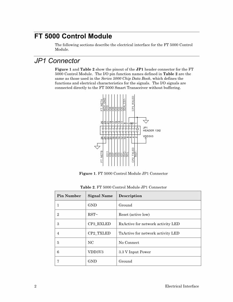
JP1 Connector Figure 1 and Table 2 show the pinout of the JP1 header connector for the FT 5000 Control Module. The I/O pin function names defined in Table 2 are the same as those used in the Series 5000 Chip Data Book, which defines the functions and electrical characteristics for the signals. The I/O signals are connected directly to the FT 5000 Smart Transceiver without buffering.
MO
V_G
ND
IO2
IO0
CP
2_T
XLE
D
SV
C-
RS
T-
FT
_NE
TA
IO10
IO8
IO6
IO4
SC
LS
DA
_CS
1-
IO11
FT
_NE
TB
IO3
IO1
IO5
IO9
IO7
VDD3V3C
P3_
RX
LED
JP1HEADER 13X2
2468101214161820222426
135791113151719212325
Figure 1. FT 5000 Control Module JP1 Connector
Table 2. FT 5000 Control Module JP1 Connector
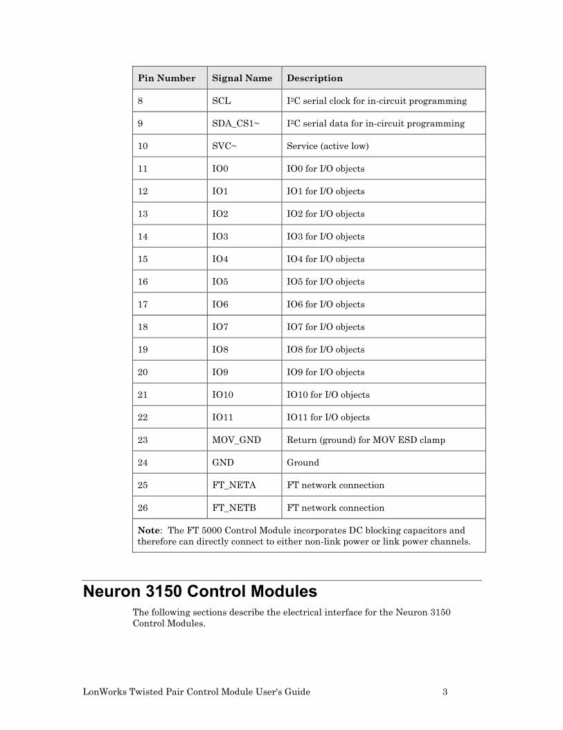
Pin Number Signal Name Description
1 GND Ground
2 RST~ Reset (active low)
3 CP3_RXLED RxActive for network activity LED
4 CP2_TXLED TxActive for network activity LED
5 NC No Connect
6 VDD3V3 3.3 V Input Power
7 GND Ground
LonWorks Twisted Pair Control Module User's Guide 3
Pin Number Signal Name Description
8 SCL I2C serial clock for in-circuit programming
9 SDA_CS1~ I2C serial data for in-circuit programming
10 SVC~ Service (active low)
11 IO0 IO0 for I/O objects
12 IO1 IO1 for I/O objects
13 IO2 IO2 for I/O objects
14 IO3 IO3 for I/O objects
15 IO4 IO4 for I/O objects
16 IO5 IO5 for I/O objects
17 IO6 IO6 for I/O objects
18 IO7 IO7 for I/O objects
19 IO8 IO8 for I/O objects
20 IO9 IO9 for I/O objects
21 IO10 IO10 for I/O objects
22 IO11 IO11 for I/O objects
23 MOV_GND Return (ground) for MOV ESD clamp
24 GND Ground
25 FT_NETA FT network connection
26 FT_NETB FT network connection
Note: The FT 5000 Control Module incorporates DC blocking capacitors and therefore can directly connect to either non-link power or link power channels.
Neuron 3150 Control Modules The following sections describe the electrical interface for the Neuron 3150 Control Modules.
4 Electrical Interface
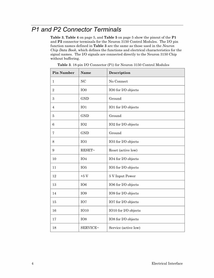
P1 and P2 Connector Terminals Table 3, Table 4 on page 5, and Table 5 on page 5 show the pinout of the P1 and P2 connector terminals for the Neuron 3150 Control Modules. The I/O pin function names defined in Table 3 are the same as those used in the Neuron Chip Data Book, which defines the functions and electrical characteristics for the signal names. The I/O signals are connected directly to the Neuron 3150 Chip without buffering.
Table 3. 18-pin I/O Connector (P1) for Neuron 3150 Control Modules
Pin Number Name Description
1 NC No Connect
2 IO0 IO0 for I/O objects
3 GND Ground
4 IO1 IO1 for I/O objects
5 GND Ground
6 IO2 IO2 for I/O objects
7 GND Ground
8 IO3 IO3 for I/O objects
9 RESET~ Reset (active low)
10 IO4 IO4 for I/O objects
11 IO5 IO5 for I/O objects
12 +5 V 5 V Input Power
13 IO6 IO6 for I/O objects
14 IO9 IO9 for I/O objects
15 IO7 IO7 for I/O objects
16 IO10 IO10 for I/O objects
17 IO8 IO8 for I/O objects
18 SERVICE~ Service (active low)
LonWorks Twisted Pair Control Module User's Guide 5
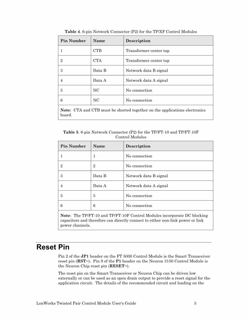
Table 4. 6-pin Network Connector (P2) for the TP/XF Control Modules
Pin Number Name Description
1 CTB Transformer center tap
2 CTA Transformer center tap
3 Data B Network data B signal
4 Data A Network data A signal
5 NC No connection
6 NC No connection
Note: CTA and CTB must be shorted together on the applications electronics board.
Table 5. 6-pin Network Connector (P2) for the TP/FT-10 and TP/FT-10F Control Modules
Pin Number Name Description
1 1 No connection
2 2 No connection
3 Data B Network data B signal
4 Data A Network data A signal
5 5 No connection
6 6 No connection
Note: The TP/FT-10 and TP/FT-10F Control Modules incorporate DC blocking capacitors and therefore can directly connect to either non-link power or link power channels.
Reset Pin Pin 2 of the JP1 header on the FT 5000 Control Module is the Smart Transceiver reset pin (RST~). Pin 9 of the P1 header on the Neuron 3150 Control Module is the Neuron Chip reset pin (RESET~).
The reset pin on the Smart Transceiver or Neuron Chip can be driven low externally or can be used as an open drain output to provide a reset signal for the application circuit. The details of the recommended circuit and loading on the
6 Electrical Interface
reset pin are described in the Series 5000 Chip Data Book or the Neuron Chip Data Book.
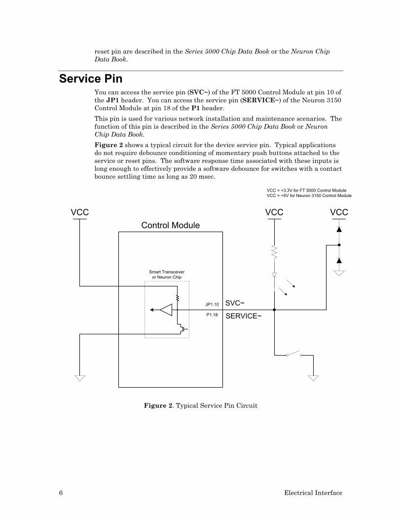
Service Pin You can access the service pin (SVC~) of the FT 5000 Control Module at pin 10 of the JP1 header. You can access the service pin (SERVICE~) of the Neuron 3150 Control Module at pin 18 of the P1 header. This pin is used for various network installation and maintenance scenarios. The function of this pin is described in the Series 5000 Chip Data Book or Neuron Chip Data Book. Figure 2 shows a typical circuit for the device service pin. Typical applications do not require debounce conditioning of momentary push buttons attached to the service or reset pins. The software response time associated with these inputs is long enough to effectively provide a software debounce for switches with a contact bounce settling time as long as 20 msec.
SVC~
VCC VCCControl Module
VCC
SERVICE~
Smart Transceiver or Neuron Chip
P1.18
JP1.10
VCC = +3.3V for FT 5000 Control ModuleVCC = +5V for Neuron 3150 Control Module
Figure 2. Typical Service Pin Circuit
LonWorks Twisted Pair Control Module User's Guide 7
2
Mechanical Considerations
This chapter discusses the mechanical footprint and connectors of the Twisted Pair Control Modules. Details of mounting to an application electronics board are provided.
8 Mechanical Considerations
FT 5000 Control Module The following sections describe the mechanical interface for the FT 5000 Control Module.
Floorplan Layout Figure 3 shows three views of the floorplan layout of the FT 5000 Control Module with some of its prominent features labeled.
FT-X3
11
2
3
4
8
7
6
5
FT 5000
AT24C512
Y1
1RV1
C7,17
43.18 mm(1.7 in)
29.85 mm(1.175 in)
Back View Front ViewSide View
16 mm(0.63 in)
Figure 3. FT 5000 Control Module Floorplan Layout
Mechanical Footprint Figure 4 shows the mechanical footprint for an FT 5000 Control Module. You can solder the module directly to your PCB as a through-hole part or mount it in a connector. The module includes a male Samtec, Inc. TSW-113-08-T-D-RA square post header, which fits into a 13x2 pin female connector, such as a Samtec, Inc. SSM-113-L-DV surface mount socket strip.
Figure 4. FT 5000 Control Module Mechanical Footprint
The figure also shows positioning for Richco® Inc. VMCGE-30M-01 vertical mount card guides for the Control Module. The card guides are optional, depending on your application.
Neuron 3150 Control Module The following sections describe the mechanical interface for the Neuron 3150 Control Modules.
LonWorks Twisted Pair Control Module User's Guide 9
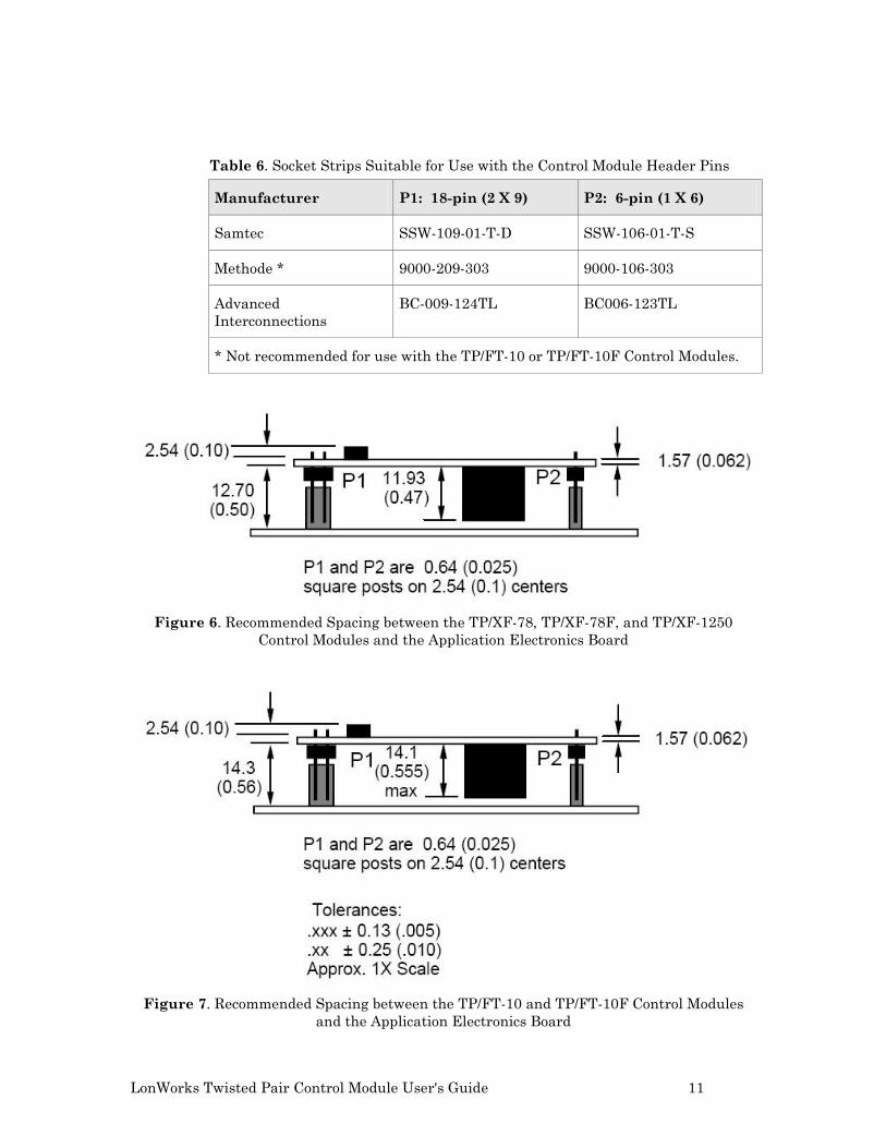
Mechanical Footprint The Neuron 3150 Twisted Pair Control Modules share a common footprint and connectors as shown in Figure 5 on page 10. The most common control module mounting scenario uses socket strips on the application electronics board which connect with P1 and P2 as shown in Figure 6 and Figure 7 on page 11. Example vendor information for socket strips that mate with the 0.025 inch (0.64 mm) square header posts of P1 and P2 are listed in Table 6 on page 11.
If necessary, taller socket strips can be used to gain more clearance between the control module and the application board. Decisions about component placement on the application electronics board must also consider the electromagnetic interference (EMI) and electrostatic discharge (ESD) issues discussed in Chapter 5, Design Issues, on page 27.
Figure 6 and Figure 7 show the maximum height of parts on both sides of the control modules. Application designs using the transformer-isolated twisted pair transceivers should maintain a minimum of 0.15 inch (3.81 mm) clearance from P2 pins and traces on the network side of the transformer to achieve the minimum isolation specified for these modules. Refer to EMI Design Issues on page 28 and Neuron 3150 Control Module Keepout Areas on page 31 for isolation requirements.
Three plated mounting holes that accept No. 6 (3.5 mm) mounting screws are electrically connected to the control module ground plane. When the 0.025 inch (0.64 mm) square posts of P1 and P2 are inserted into the sockets they provide enough holding strength (3 oz (85 g)/pin) to secure the control module against shock and vibration to the operating limits of the components on the control module. However, at least one metal standoff and fastening screw located at the mounting hole near the P2 connector is recommended to meet EMI limits and for ESD protection (see Chapter 5).
For the TP/FT-10 control modules, the recommended metal standoff height is 0.56 inch (14.3 mm) to provide adequate clearance. Note that the Methode Socket (referenced in Table 6) in this case is not recommended, because its minimum insertion depth requirement is not met. Use of metal 0.50 inch (12.7 mm) #6 standoffs together with metal spacers can achieve this. Alternately, metal 0.56 inch (14.3 mm) #6 standoffs alone will be adequate. For the TP/XF and TP/FT-10F control modules, 0.50 inch (12.7 mm) #6 metal standoffs alone are recommended.
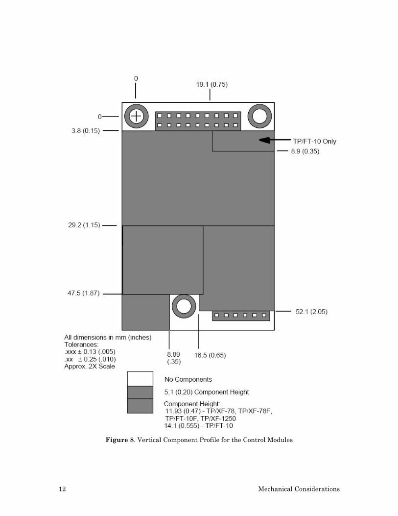
Figure 8 on page 12 presents the height restrictions of the component side of the control module. The board is divided into two height zones: the maximum height of components in the first zone is 0.20 inch (5.1 mm). The second zone's components are 0.47 inch (11.93 mm) for the TP/XF and TP/FT-10F control modules and 0.555 inch (14.1 mm) for the TP/FT-10 control module. Care should be taken to ensure that no components on the application electronics board interfere with the height restricted areas of the control modules.
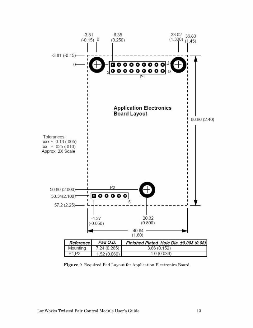
Figure 9 on page 13 shows the recommended PCB pad layout for the application electronics board to interconnect a control module with an application board that has socket strips mounted on the component side.
10 Mechanical Considerations
Figure 5. Neuron 3150 Control Module Mechanical Footprint
LonWorks Twisted Pair Control Module User's Guide 11
Table 6. Socket Strips Suitable for Use with the Control Module Header Pins
Manufacturer P1: 18-pin (2 X 9) P2: 6-pin (1 X 6)
Samtec SSW-109-01-T-D SSW-106-01-T-S
Methode * 9000-209-303 9000-106-303
Advanced Interconnections
BC-009-124TL BC006-123TL
* Not recommended for use with the TP/FT-10 or TP/FT-10F Control Modules.
Figure 6. Recommended Spacing between the TP/XF-78, TP/XF-78F, and TP/XF-1250
Control Modules and the Application Electronics Board
Figure 7. Recommended Spacing between the TP/FT-10 and TP/FT-10F Control Modules
and the Application Electronics Board
12 Mechanical Considerations
Figure 8. Vertical Component Profile for the Control Modules
LonWorks Twisted Pair Control Module User's Guide 13
Figure 9. Required Pad Layout for Application Electronics Board

LonWorks Twisted Pair Control Module User's Guide 15
3
Power Requirements
This section describes the power requirements for the control modules as well as considerations for noise filtering in order to comply with both conducted and radiated emissions requirements.
16 Power Requirements
FT 5000 Control Module The following sections describe the power requirements for the FT 5000 Control Module.
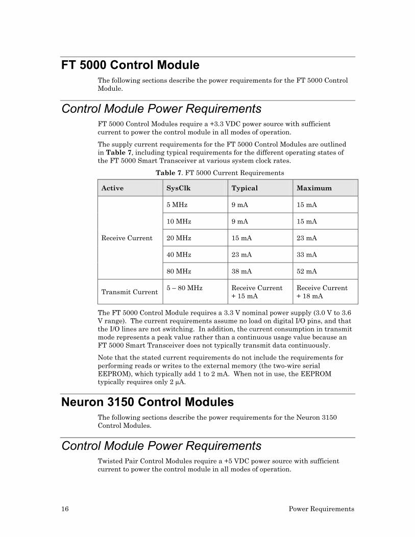
Control Module Power Requirements FT 5000 Control Modules require a +3.3 VDC power source with sufficient current to power the control module in all modes of operation.
The supply current requirements for the FT 5000 Control Modules are outlined in Table 7, including typical requirements for the different operating states of the FT 5000 Smart Transceiver at various system clock rates.
Table 7. FT 5000 Current Requirements
Active SysClk Typical Maximum
Receive Current
5 MHz 9 mA 15 mA
10 MHz 9 mA 15 mA
20 MHz 15 mA 23 mA
40 MHz 23 mA 33 mA
80 MHz 38 mA 52 mA
Transmit Current 5 – 80 MHz Receive Current + 15 mA
Receive Current + 18 mA
The FT 5000 Control Module requires a 3.3 V nominal power supply (3.0 V to 3.6 V range). The current requirements assume no load on digital I/O pins, and that the I/O lines are not switching. In addition, the current consumption in transmit mode represents a peak value rather than a continuous usage value because an FT 5000 Smart Transceiver does not typically transmit data continuously.
Note that the stated current requirements do not include the requirements for performing reads or writes to the external memory (the two-wire serial EEPROM), which typically add 1 to 2 mA. When not in use, the EEPROM typically requires only 2 μA.
Neuron 3150 Control Modules The following sections describe the power requirements for the Neuron 3150 Control Modules.
Control Module Power Requirements Twisted Pair Control Modules require a +5 VDC power source with sufficient current to power the control module in all modes of operation.
LonWorks Twisted Pair Control Module User's Guide 17
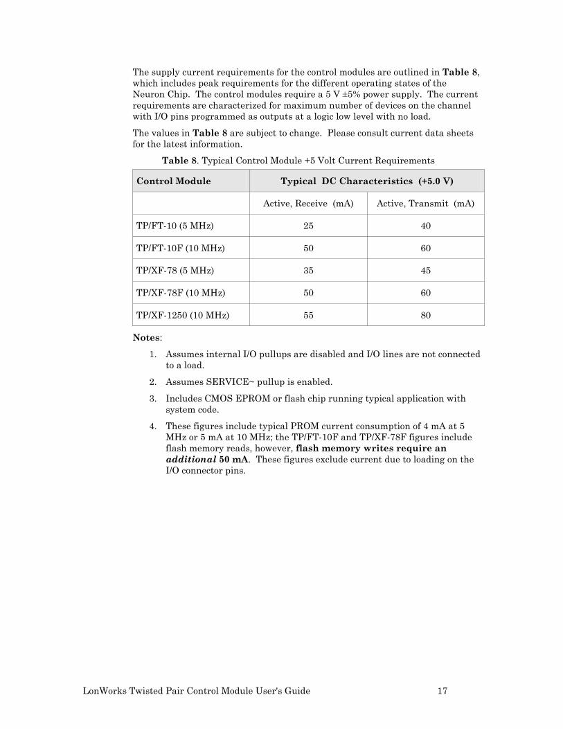
The supply current requirements for the control modules are outlined in Table 8, which includes peak requirements for the different operating states of the Neuron Chip. The control modules require a 5 V ±5% power supply. The current requirements are characterized for maximum number of devices on the channel with I/O pins programmed as outputs at a logic low level with no load.
The values in Table 8 are subject to change. Please consult current data sheets for the latest information.
Table 8. Typical Control Module +5 Volt Current Requirements
Control Module Typical DC Characteristics (+5.0 V)
Active, Receive (mA) Active, Transmit (mA)
TP/FT-10 (5 MHz) 25 40
TP/FT-10F (10 MHz) 50 60
TP/XF-78 (5 MHz) 35 45
TP/XF-78F (10 MHz) 50 60
TP/XF-1250 (10 MHz) 55 80
Notes:
1. Assumes internal I/O pullups are disabled and I/O lines are not connected to a load.
2. Assumes SERVICE~ pullup is enabled.
3. Includes CMOS EPROM or flash chip running typical application with system code.
4. These figures include typical PROM current consumption of 4 mA at 5 MHz or 5 mA at 10 MHz; the TP/FT-10F and TP/XF-78F figures include flash memory reads, however, flash memory writes require an additional 50 mA. These figures exclude current due to loading on the I/O connector pins.

LonWorks Twisted Pair Control Module User's Guide 19
4
Network Cabling and Connection
This chapter addresses cabling and termination for the FT 5000 Control Module and the Neuron 3150 Control Modules (TP/FT-10, TP/FT-10F, TP/XF-78, TP/XF-78F, and TP/XF-1250 Twisted Pair Control Modules).
20 Network Cabling and Connection
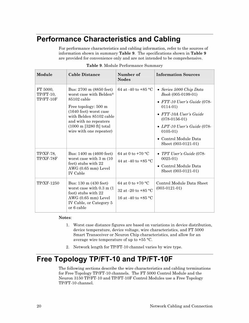
Performance Characteristics and Cabling For performance characteristics and cabling information, refer to the sources of information shown in summary Table 9. The specifications shown in Table 9 are provided for convenience only and are not intended to be comprehensive.
Table 9. Module Performance Summary
Module Cable Distance Number of Nodes
Information Sources
FT 5000, TP/FT-10, TP/FT-10F
Bus: 2700 m (8850 feet) worst case with Belden® 85102 cable
Free topology: 500 m (1640 feet) worst case with Belden 85102 cable and with no repeaters (1000 m [3280 ft] total wire with one repeater)
64 at -40 to +85 °C • Series 5000 Chip Data Book (005-0199-01)
• FTT-10 User's Guide (078-0114-01)
• FTT-10A User's Guide (078-0156-01)
• LPT-10 User's Guide (078-0105-01)
• Control Module Data Sheet (003-0121-01)
TP/XF-78, TP/XF-78F
Bus: 1400 m (4600 feet) worst case with 3 m (10 feet) stubs with 22 AWG (0.65 mm) Level IV Cable
64 at 0 to +70 °C
44 at -40 to +85 °C
• TPT User's Guide (078-0025-01)
• Control Module Data Sheet (003-0121-01)
TP/XF-1250 Bus: 130 m (430 feet) worst case with 0.3 m (1 foot) stubs with 22 AWG (0.65 mm) Level IV Cable, or Category 5 or 6 cable
64 at 0 to +70 °C
32 at -20 to +85 °C
16 at -40 to +85 °C
Control Module Data Sheet (003-0121-01)
Notes:
1. Worst case distance figures are based on variations in device distribution, device temperature, device voltage, wire characteristics, and FT 5000 Smart Transceiver or Neuron Chip characteristics, and allow for an average wire temperature of up to +55 °C.
2. Network length for TP/FT-10 channel varies by wire type.
Free Topology TP/FT-10 and TP/FT-10F The following sections describe the wire characteristics and cabling terminations for Free Topology TP/FT-10 channels. The FT 5000 Control Module and the Neuron 3150 TP/FT-10 and TP/FT-10F Control Modules use a Free Topology TP/FT-10 channel.
LonWorks Twisted Pair Control Module User's Guide 21
Wire Characteristics Due to the many cabling and termination options available for the TP/FT-10 channel, please refer to the Series 5000 Chip Data Book, FTT-10 Free Topology Transceiver User's Guide, or FTT-10A Free Topology Transceiver User's Guide, as applicable, for information on wire characteristics and terminations.
The Junction Box and Wiring Guidelines for Twisted Pair LonWorks Networks engineering bulletin (005-0023-01) provides a list of cable vendors for each type of supported cable. This bulletin is available from the Echelon Web site (www.echelon.com).
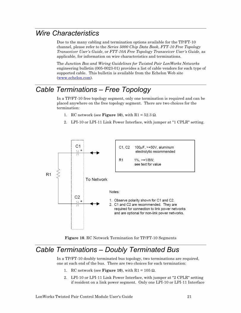
Cable Terminations – Free Topology In a TP/FT-10 free topology segment, only one termination is required and can be placed anywhere on the free topology segment. There are two choices for the termination:
1. RC network (see Figure 10), with R1 = 52.3 Ω.
2. LPI-10 or LPI-11 Link Power Interface, with jumper at "1 CPLR" setting.
Figure 10. RC Network Termination for TP/FT-10 Segments
Cable Terminations – Doubly Terminated Bus In a TP/FT-10 doubly terminated bus topology, two terminations are required, one at each end of the bus. There are two choices for each termination:
1. RC network (see Figure 10), with R1 = 105 Ω.
2. LPI-10 or LPI-11 Link Power Interface, with jumper at "2 CPLR" setting if resident on a link power segment. Only one LPI-10 or LPI-11 Interface
22 Network Cabling and Connection
is supported per segment, so at least one of the terminations must be the RC-type.
TP/XF-78, TP/XF-78F, and TP/XF-1250 The following sections describe the wire characteristics and cabling terminations for TP/XF-78, and TP/XF-1250 channels. In addition, the device distribution rule for TP/XF-1250 network segments is described.
Wire Characteristics The Neuron 3150 TP/XF-78, TP/XF-78F, and TP/XF-1250 control modules are designed for distributed control applications using low-cost, Level IV twisted pair wire. The TP/XF-1250 Control Module can also use AWG 24 (0.511 mm) ANSI/TIA/EIA-568-B.2-2001 Category 5 or Category 6 twisted-pair wire. The characteristics of the wire used to implement a network affects the overall system performance with respect to total distance, stub length, and total number of nodes supported on a single channel.
The TP/XF-78 and TP/XF-78F control modules have been qualified using the following cable types:
• Primary bus: Level IV, AWG 22 (0.65 mm)
• Stubs (where permitted): Level IV, AWG 24 (0.511 mm) cable or Level IV, AWG 22 cable
The TP/XF-1250 Control Module has been qualified using the following cable types:
• Primary bus: Level IV, AWG 22 (0.65 mm); or AWG 24 (0.511 mm) ANSI/TIA/EIA-568-B.2-2001 Category 5 or Category 6 twisted-pair cable
• Stubs (where permitted): Level IV, AWG 24 (0.511 mm) cable; Level IV, AWG 22 cable; or AWG 24 (0.511 mm) ANSI/TIA/EIA-568-B.2-2001 Category 5 or Category 6 twisted-pair cable
For all of the control modules, under no circumstances should smaller gauge Level IV cable be substituted for Level IV, AWG 22 (0.65 mm) twisted pair cable for the bus, or should Category IV cable be used in place of Level IV cable.
Echelon periodically qualifies new cables for twisted pair transceivers, and it is advisable to check with Echelon from time to time to determine if new cables are available for use with the control modules.
The characteristics and suppliers of Level IV cable are described in the Junction Box and Wiring Guidelines for Twisted Pair LonWorks Networks engineering bulletin (005-0023-01).
Device Distribution Rule for TP/XF-1250 Segments Because of the transmission characteristics of the TP/XF-1250 channel, communication failures can result from reflections of the TP/XF-1250 module’s 1.25 Mbps transmitted signal under conditions of concentrated device loading. These communication failures are eliminated when devices are used in a distributed configuration. For this reason, it is essential to follow a simple topology rule when using TP/XF-1250 control modules, TPT/XF-1250
LonWorks Twisted Pair Control Module User's Guide 23
transceivers, or TPM-1250 SMX transceivers to eliminate the possibility of reflection-related transmission failures. No such topology rule applies to the use of TP/XF-78 control modules, TPT/XF-78 transceivers, or TPM-78 SMX transceivers.
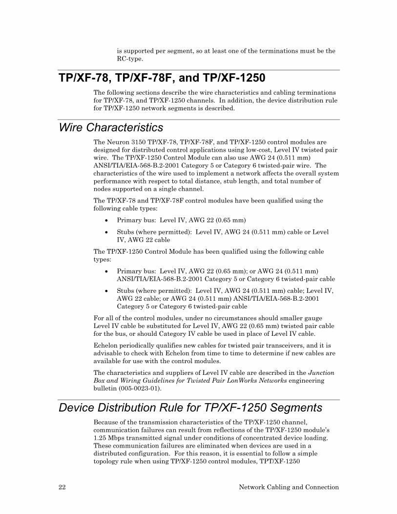
Referred to as the “8-in-16” topology rule, this rule requires that no more than 8 TP/XF-1250 Control Modules, TP/XF-1250 Transceivers, or TPM-1250 SMX Transceivers be located within any 16 meter length of cable. This means that no matter where along the bus the 16 meter measurement is taken, there should be no more than 8 devices. Figure 11 provides a diagram of such a measurement technique. In the figure, the numbers in the boxes represent the number of devices connected to the bus and the “T” represents the bus termination.
Figure 11. 8-in-16 Topology Rule Example
In the example, we see an installation with six groups of devices, varying in number from 2 to 8 devices, in a doubly terminated bus. By using a 16 meter measurement stick that we can move from side-to-side over the length of the bus, we can determine whether the 8-in-16 rule has been met (designated by the word “OK”) or violated (shown by the designation “PROBLEM”). In the case of the PROBLEM area, a total of 13 devices are located within a 16 meter length of the bus, which amounts to five more devices than are permitted under the 8-in-16 rule.
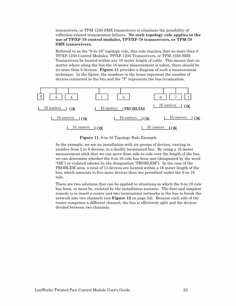
There are two solutions that can be applied to situations in which the 8-in-16 rule has been, or must be, violated by the installation scenario. The first and simplest remedy is to insert a router and two termination networks in the bus to break the network into two channels (see Figure 12 on page 24). Because each side of the router comprises a different channel, the bus is effectively split and the devices divided between two channels.
24 Network Cabling and Connection
Figure 12. Using a Router to Meet the 8-in-16 Topology Rule
The second remedy to a violation of the 8-in-16 rule is to add additional cable to the bus such that the rule is no longer violated (see Figure 13). It is important to ensure that the maximum bus length (130 meters of 22 AWG [0.65 mm] Level IV or AWG 24 [0.511 mm] ANSI/TIA/EIA-568-B.2-2001 Category 5 or Category 6 twisted-pair cable) is not exceeded by the additional cable. Because of the complex interactions between the bus and the transceivers with regard to reflections and transmission line delays, it is not possible to substitute an LC network in place of the additional cable to resolve this rule violation.
Figure 13. Using Additional Bus Cable to Meet the 8-in-16 Topology Rule
Cable Terminations – TP/XF-78, -1250 Segments Twisted pair network segments require termination for proper data transmission performance. For doubly terminated bus topologies, a termination must reside at both endpoints of the bus. The terminations required for TP/XF-78, TP/XF-78F, and TP/XF-1250 segments are shown in Figure 14 on page 25.
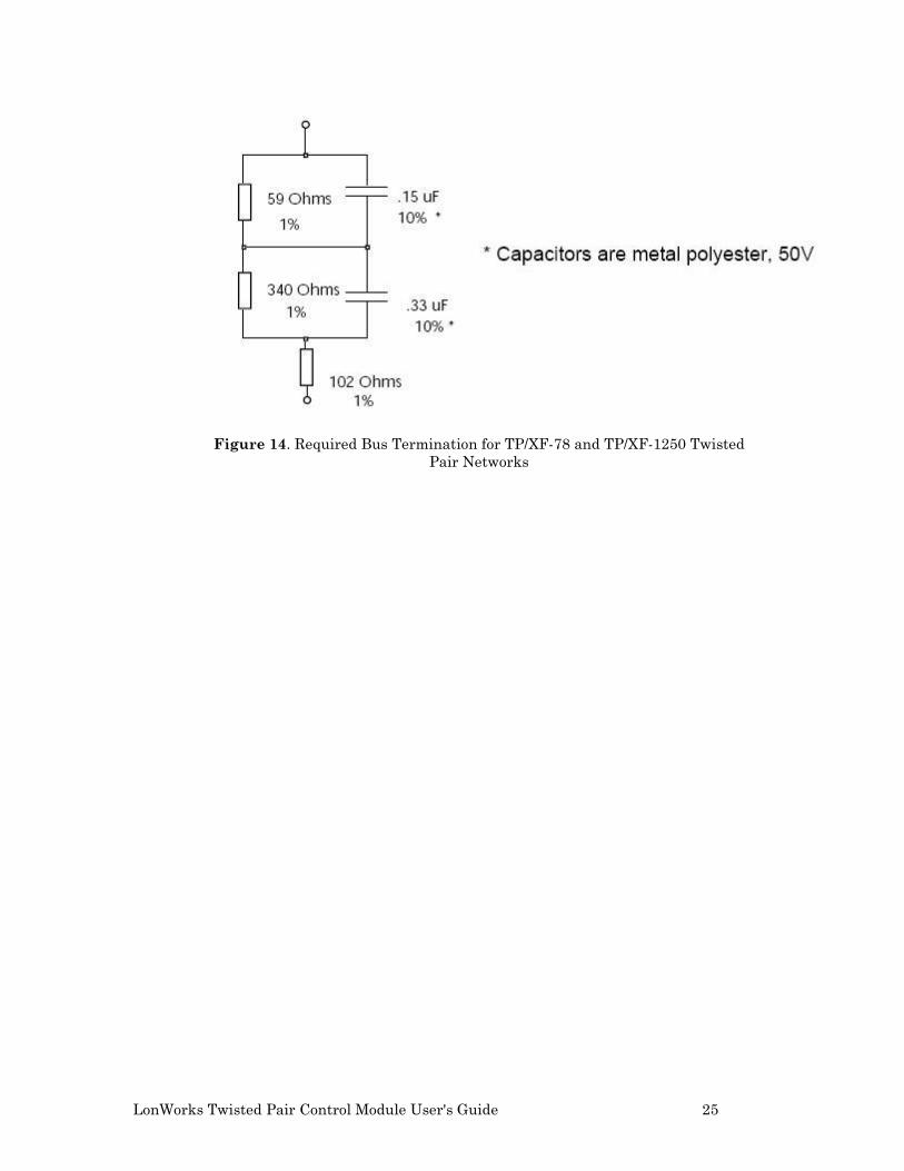
LonWorks Twisted Pair Control Module User's Guide 25
Figure 14. Required Bus Termination for TP/XF-78 and TP/XF-1250 Twisted
Pair Networks

LonWorks Twisted Pair Control Module User's Guide 27
5
Design Issues
This chapter describes design issues, including a discussion of Electromagnetic Interference (EMI), and Electrostatic Discharge (ESD), and Designing for Interoperability. This chapter applies to both FT 5000 Control Modules and Neuron 3150 Control Modules.
28 Design Issues
EMI Design Issues The high-speed digital signals associated with microcontroller designs can generate unintentional Electromagnetic Interference (EMI). High-speed voltage changes generate RF currents that can cause radiation from a product if a length of wire or piece of metal can serve as an antenna.
Products that use the Twisted Pair Control Modules generally need to demonstrate compliance with EMI limits enforced by various regulatory agencies. In the USA, the Federal Communications Commission (FCC) requires that unintentional radiators comply with Part 15 level “A” for industrial products, and level “B” for products that can be used in residential environments. In Europe, the CENELEC committee requires that unintentional radiators comply with the EN 55022 standard. Similar regulations are imposed in most countries throughout the world.
Echelon has designed the Twisted Pair Control Modules with low enough RF noise levels for design into level “B” products. Echelon encourages level “B” compliance for all LONWORKS compatible products. This section describes design considerations for control module-based products to meet EMI regulations.
Designing Systems for EMC Echelon has demonstrated that designs using the control modules can meet both FCC and EN55022 level “B” limits. Careful design of application electronics is important to guarantee that a control module-based node will achieve the desired electromagnet compatibility (EMC). This section provides useful design tips for EMC. The FT 5000, TP/FT-10, and TP/FT-10F Control Modules have been designed to comply with IEC 61000-4-2, IEC 61000-4-3, IEC 61000-4-4, IEC 61000-4-5, and IEC 61000-4-6 standards. For more information, see the Series 5000 Chip Data Book, FTT-10 Free Topology Transceiver User's Guide, or FTT-10A Free Topology Transceiver User's Guide, as applicable.
EMC Design Tips The following design tips can greatly aid in EMC design:
• Most of the RF noise originates in the CPU portion of the control module, and in any high-frequency or high-speed application circuitry in the device.
• Most of the EMI will be radiated by the network cable and the power cable.
• Filtering is generally necessary to keep RF noise from getting out on the power cable.
• EMI “Keepout” area restrictions should be observed to prevent internal RF noise from coupling onto the network cable.
• The control module must be well grounded within the device to ensure that its built-in EMI filtering works properly.
• Early EMI testing of prototypes at a certified test facility is an extremely important step in the design of level “B” products. This testing ensures
LonWorks Twisted Pair Control Module User's Guide 29
that grounding and enclosure design questions are addressed early enough to avoid most last-minute changes (and their associated schedule delays).
It is possible for a plastic enclosure to be used with Twisted Pair Control Modules in level “B” applications in some specialized configurations. Because external cables must be kept away from the “RF hot” keepout area on the modules (see Figure 16 on page 32), the product configuration must constrain the routing of cables so that they cannot pass across the surface of the plastic enclosure near the module. During FCC EMI testing, cable position is typically varied to generate maximum emission levels (within constraints of normal product usage).
For Neuron 3150 Control Modules, the three standoff holes are generally not needed for mechanical support, but the hole nearest connector P2 is important for EMI grounding of the control module. Best results are achieved by a solid ground connection from the control module to the application mother board and to a metalized enclosure using the P2 standoff.
The Twisted Pair Control Modules include adequate filtering on the network data communication lines for most device designs to meet level “B” emission limits. In rare cases, such as designs including circuits with extremely fast edges, additional noise attenuation is required. In such cases it may be necessary to use a common-mode choke connected in series with the data communication lines adjacent to the device’s external network connector. Common-mode chokes can provide an additional 10 to 15 dB of EMI attenuation over the 30 to 500 MHz range. A choke adds a few pF of differential capacitance to the data communication lines, and therefore reduces network performance and can affect interoperability. In general, application designs should not require a common-mode choke.
FT 5000 Control Module PC Board Layout Guidelines Electrostatic discharge (ESD) and electromagnetic interference (EMI) are two of the most important design considerations when laying out the PCB for a device.
Tolerance of ESD and other types of network transients requires careful layout for power, ground, and other device circuitry. In general, ESD currents return to Earth ground or to other nearby metal structures. The device’s ground scheme must be able to pass this ESD current between the network connection and the device’s external ground connection without generating significant voltage gradients across the device’s PCB. The low-inductance star-ground configuration accomplishes this task. The star-ground configuration conducts transients out of the device with minimal disruption to other function blocks.
The following list describes some of the general features of a careful PCB design layout for an FT 5000 Control Module:
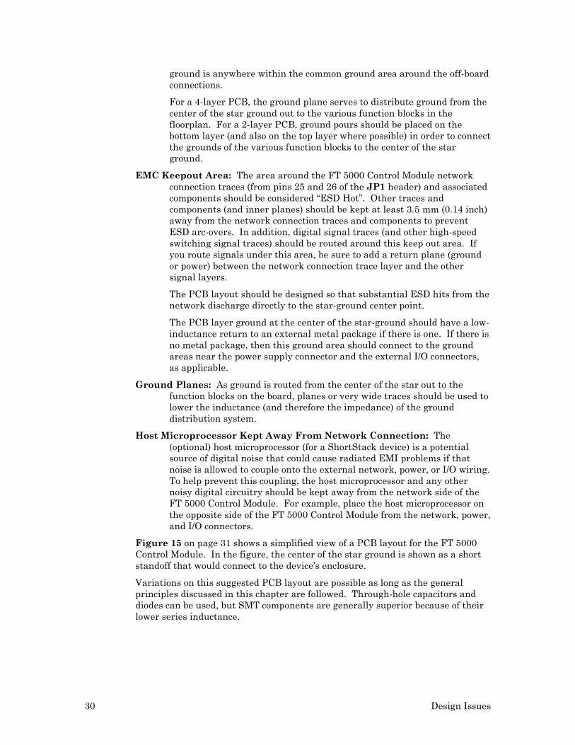
Star-Ground Configuration: The various blocks of the device that directly interface with off-board connections (the network, any external I/O, and the power supply cable) should be arranged so that the connections are together along one edge of the PCB. This arrangement allows any transient current that comes in by one connection to flow back out of the device by one of the other connections.
If connection is made between the PCB ground and a metal enclosure, that connection should be made using a low-inductance connection (like a short standoff) in the center of the star ground. The center of the star
30 Design Issues
ground is anywhere within the common ground area around the off-board connections.
For a 4-layer PCB, the ground plane serves to distribute ground from the center of the star ground out to the various function blocks in the floorplan. For a 2-layer PCB, ground pours should be placed on the bottom layer (and also on the top layer where possible) in order to connect the grounds of the various function blocks to the center of the star ground.
EMC Keepout Area: The area around the FT 5000 Control Module network connection traces (from pins 25 and 26 of the JP1 header) and associated components should be considered “ESD Hot”. Other traces and components (and inner planes) should be kept at least 3.5 mm (0.14 inch) away from the network connection traces and components to prevent ESD arc-overs. In addition, digital signal traces (and other high-speed switching signal traces) should be routed around this keep out area. If you route signals under this area, be sure to add a return plane (ground or power) between the network connection trace layer and the other signal layers.
The PCB layout should be designed so that substantial ESD hits from the network discharge directly to the star-ground center point.
The PCB layer ground at the center of the star-ground should have a low-inductance return to an external metal package if there is one. If there is no metal package, then this ground area should connect to the ground areas near the power supply connector and the external I/O connectors, as applicable.
Ground Planes: As ground is routed from the center of the star out to the function blocks on the board, planes or very wide traces should be used to lower the inductance (and therefore the impedance) of the ground distribution system.
Host Microprocessor Kept Away From Network Connection: The (optional) host microprocessor (for a ShortStack device) is a potential source of digital noise that could cause radiated EMI problems if that noise is allowed to couple onto the external network, power, or I/O wiring. To help prevent this coupling, the host microprocessor and any other noisy digital circuitry should be kept away from the network side of the FT 5000 Control Module. For example, place the host microprocessor on the opposite side of the FT 5000 Control Module from the network, power, and I/O connectors.
Figure 15 on page 31 shows a simplified view of a PCB layout for the FT 5000 Control Module. In the figure, the center of the star ground is shown as a short standoff that would connect to the device’s enclosure.
Variations on this suggested PCB layout are possible as long as the general principles discussed in this chapter are followed. Through-hole capacitors and diodes can be used, but SMT components are generally superior because of their lower series inductance.
LonWorks Twisted Pair Control Module User's Guide 31
FT 5
000
Con
trol M
odul
e
NetworkConnector
Host Microprocessor(Optional)
Power SupplyCircuitry
I/O Circuitry
I/OConnectors
Power SupplyConnector
Center of Star Ground
EMCKeepout
Area
Figure 15. Example PCB Layout Design for an FT 5000 Control Module
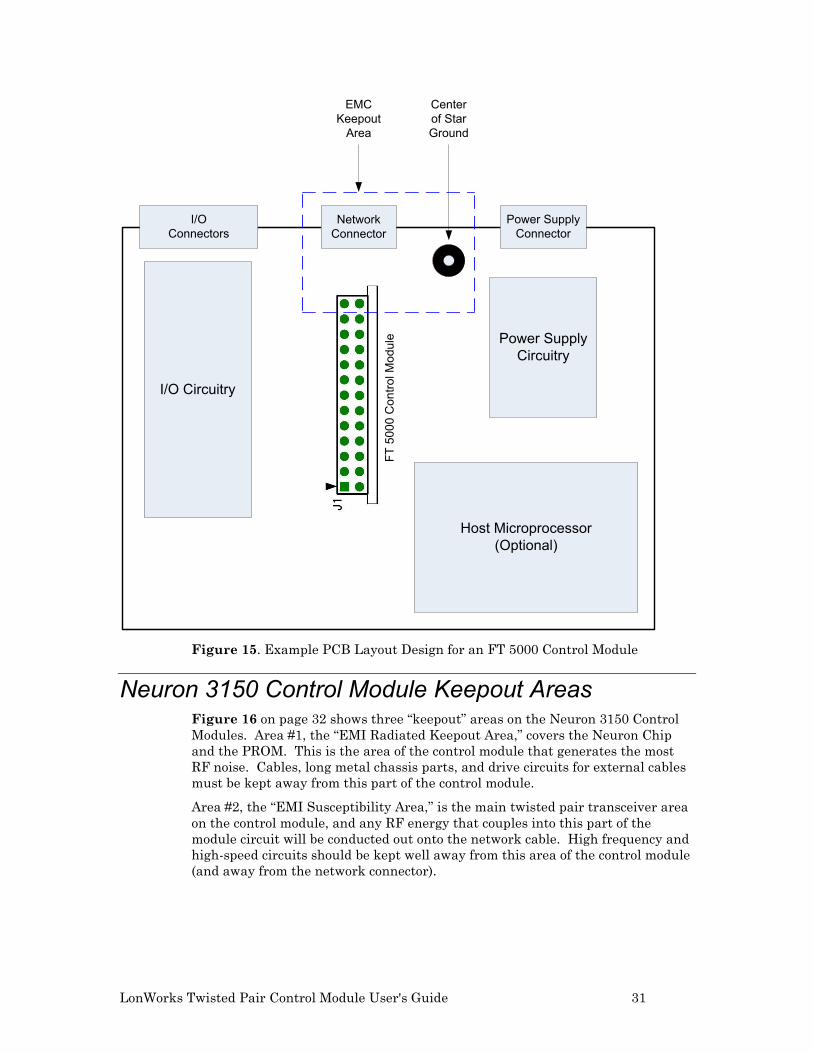
Neuron 3150 Control Module Keepout Areas Figure 16 on page 32 shows three “keepout” areas on the Neuron 3150 Control Modules. Area #1, the “EMI Radiated Keepout Area,” covers the Neuron Chip and the PROM. This is the area of the control module that generates the most RF noise. Cables, long metal chassis parts, and drive circuits for external cables must be kept away from this part of the control module.
Area #2, the “EMI Susceptibility Area,” is the main twisted pair transceiver area on the control module, and any RF energy that couples into this part of the module circuit will be conducted out onto the network cable. High frequency and high-speed circuits should be kept well away from this area of the control module (and away from the network connector).
32 Design Issues
Figure 16. Control Module Keepout Areas
Area #3 is the “High Voltage Isolation Area.” The transceiver coupling transformer on all Neuron 3150 Control Modules provides electrical isolation between the control module’s local ground (primary side) and the network wiring (secondary side). The transformers and associated filter components are designed to withstand moderately large primary-to-secondary voltages (see the control module data sheets for the exact ratings). To take advantage of this isolation, it is important to keep application circuitry, logic ground, metal chassis parts, and other primary-side components at least 3.8 mm (0.15 inches) away from the secondary area on the control module and the network connector.
ESD Design Issues Electrostatic Discharge (ESD) is encountered frequently in industrial and commercial use of electronic systems. Reliable system designs must consider the effects of ESD and take steps to protect sensitive components. Static discharges occur frequently in low-humidity environments when operators touch electronic equipment. The static voltages generated by humans can easily exceed 10 kV. Keyboards, connectors, and enclosures provide paths for static discharges to reach ESD-sensitive components such as the Neuron Chip. This section describes techniques to design ESD immunity into control module-based products.
LonWorks Twisted Pair Control Module User's Guide 33
Designing Systems for ESD Immunity ESD hardening includes the following techniques:
• Provide adequate creepage and clearance distances to prevent ESD hits from reaching sensitive circuitry
• Provide low impedance paths for ESD hits to ground
• Use diode clamps or transient voltage suppression devices for accessible, sensitive circuits
The best protection from ESD damage is circuit inaccessibility. If all circuit components are positioned away from package seams, the static discharges can be prevented from reaching ESD sensitive components. There are two measures of “distance” to consider for inaccessibility: creepage and clearance. Creepage is the shortest distance between two points along the contours of a surface. Clearance is the shortest distance between two points through the air. An ESD hit generally arcs farther along a surface than it does when passing straight through the air. For example, a 20 kV discharge can arc about 10 mm (0.4 inches) through dry air, but the same discharge can travel over 20 mm (0.8 inches) along a clean surface. Dirty surfaces can allow arcing over even longer creepage distances.
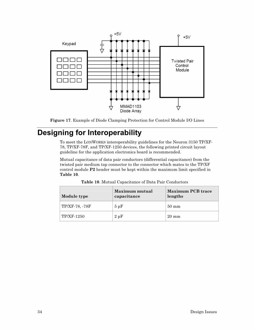
When ESD hits to circuitry cannot be avoided through creepage, clearance and ground guarding techniques (for example, at external connector pins), explicit clamping of the exposed lines is required to shunt the ESD current. Consult a good text on EMC for advice about ESD and transient protection for exposed circuit lines. In general, exposed lines require diode clamps to the power supply rails or Zener clamps to chassis ground to shunt the ESD current to ground while clamping the voltage low enough to prevent circuit damage. The control module’s I/O and control lines are connected directly to the external connector (JP1 for the FT 5000 Control Module; P1 for the Neuron 3150 Control Modules) without any ESD protection beyond that provided by the Smart Transceiver or Neuron Chip itself. If these lines are likely to be exposed to ESD in an application, protection must be added on the application electronics board. Figure 17 on page 34 shows an example of the use of diode clamps to protect the control module I/O lines in a keypad scanning application.
The control modules use diode clamping and transformer isolation to shunt ESD from the network connector (JP1 for the FT 5000 Control Module; P2 for the Neuron 3150 Control Modules) to ground. It is therefore important to provide a low impedance ground path from the JP1 connector or the mounting hole near P2 to the main system ground. The Neuron 3150 TP/FT-10 also includes spark gaps (designed to arc at approximately 1000 to 2000 V) between each of the network lines to ground and a diode-capacitor protection circuit to absorb ESD energy. The Neuron 3150 TP/FT-10F uses similar, but not identical, protection circuitry.
34 Design Issues
Figure 17. Example of Diode Clamping Protection for Control Module I/O Lines
Designing for Interoperability To meet the LONWORKS interoperability guidelines for the Neuron 3150 TP/XF-78, TP/XF-78F, and TP/XF-1250 devices, the following printed circuit layout guideline for the application electronics board is recommended.
Mutual capacitance of data pair conductors (differential capacitance) from the twisted pair medium tap connector to the connector which mates to the TP/XF control module P2 header must be kept within the maximum limit specified in Table 10.
Table 10. Mutual Capacitance of Data Pair Conductors
Module type Maximum mutual capacitance
Maximum PCB trace lengths
TP/XF-78, -78F 5 pF 50 mm
TP/XF-1250 2 pF 20 mm

LonWorks Twisted Pair Control Module User's Guide 35
6
Programming Considerations
This section explains the integration of control modules using the NodeBuilder FX Development tool. It covers considerations relating to memory specifications, device definition, channel definition, and target hardware.
36 Programming Considerations
External Memory Considerations The following sections describe considerations for the external memory devices on the FT 5000 Control Module and Neuron 3150 Control Modules.
FT 5000 Control Module The FT 5000 Control Module includes an Atmel® AT24C512BN-SH25-T two-wire serial EEPROM to hold the application image. You can program the external memory for the FT 5000 Smart Transceiver on the control module using either of the following methods:
• Program the memory part in-circuit using a serial I2C programming device, such as the Total Phase™ Aardvark™ I2C/SPI Host Adapter.
• Program the memory part over the LONWORKS network, using a network manager such as the LonMaker® Integration tool or the NodeLoad utility.
Using an Aardvark I2C/SPI Host Adapter For the Aardvark I2C/SPI Host Adapter with the Flash Center Memory Programmer software:
• Rename the .NME application image file that is generated by the NodeBuilder tool to a .HEX file.
• Select the memory part to program ("Atmel 24C512B" I2C EEPROM for the first release of the Control Module; check the part on the board to verify the part number). Important: Specify a byte padding value of “00” (the default padding value used by the Aardvark I2C/SPI Host Adapter is “FF”).
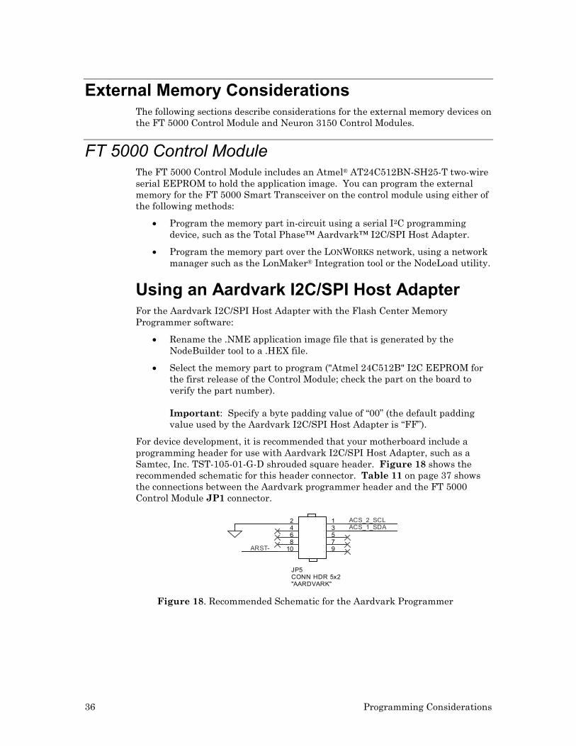
For device development, it is recommended that your motherboard include a programming header for use with Aardvark I2C/SPI Host Adapter, such as a Samtec, Inc. TST-105-01-G-D shrouded square header. Figure 18 shows the recommended schematic for this header connector. Table 11 on page 37 shows the connections between the Aardvark programmer header and the FT 5000 Control Module JP1 connector.
JP5CONN HDR 5x2"AARDVARK"
2468
10
13579
ACS_1_SDA
ARST-
ACS_2_SCL
Figure 18. Recommended Schematic for the Aardvark Programmer
LonWorks Twisted Pair Control Module User's Guide 37
Table 11. Pin Connections for Aardvark Programmer and JP1 Header
Aardvark Programmer Header FT 5000 Control Module JP1 Header
Pin Signal Pin Signal
1 ACS_2_SCL 8 SCL
3 ACS_1_SDA 9 SDA_CS1~
10 ARST~ 2 RST~
The connection between the Aardvark programmer header’s ARST~ signal and the FT 5000 Control Module JP1 connector’s RST~ signal ensures that the FT 5000 Smart Transceiver is held in reset during device programming.
Clearing the Non-Volatile Memory In general, if you have a working device, you should not need to clear the external EEPROM non-volatile memory for a Series 5000 chip. For a working device, you can receive a service-pin message and reload the non-volatile memory from the network as needed. However, if it should become necessary to clear the EEPROM non-volatile memory (for example, during device development), perform the following tasks:
1. Reset the device by pressing and holding the device’s Reset button. If the device does not have a Reset button, temporarily connect the RST~ pin (pin 2 of the JP1 header) of the control module to GND to hold the chip in the reset state.
2. Temporarily connect the EEPROM's SCL pin (pin 8 of the JP1 header) to GND.
3. Release the device’s Reset button (or remove the GND connection from the RST~ pin).
4. Wait a few seconds until the device’s Service Pin LED is illuminated (on solid, not flashing). If the device does not have a Service Pin LED, connect a logic analyzer or oscilloscope to the SVC~ pin (pin 10 of the JP1 header) of the control module and verify that it changes state (low to high) at a 76 Hz rate.
5. Disconnect the EEPROM's SCL pin from GND.
6. Use the NodeUtil utility to set the memory configuration and set the state for the device:
a. Connect the PC that will run the NodeUtil utility to the same network interface that connects to the device. For example, if you connect to the device using LON1, connect the NodeUtil utility to LON1.
b. Start the NodeUtil utility.
38 Programming Considerations
c. Press the Service Pin button on the device to send a service-pin message to the NodeUtil utility. If you cannot receive a service-pin message from the device, repeat steps 1 to 5.
d. Within the NodeUtil utility, select the L option to see all connected devices.
e. Select the G option to manage the device that just sent a service-pin message. Typically, this is device 1.
f. Select W to write to a memory location. When prompted, do not update the application checksum and do not update the configuration checksum.
g. Enter F037 for the starting address. Enter a value of 0 (zero) for address 0xF037. This value triggers device re-initialization at the next reset. Important: The memory address F037 applies to system firmware versions 18 and 19. For later versions of the firmware, this address might change; contact Echelon Support to verify the correct memory address.
h. Enter a period (.) to exit the memory write session.
i. Select E to exit device management mode.
j. Select E to exit the NodeUtil utility.
7. Reset the device by pressing the device’s Reset button. If the device does not have a Reset button, briefly connect the RST~ pin (pin 2 of the JP1 header) of the control module to GND.
Step 6 above writes values to specific bytes of the in-RAM copy of data that is in the EEPROM device. During device re-initialization and reset, the FT 5000 Smart Transceiver reads these bytes and copies the default chip configuration (including memory map and mode table) to the external EEPROM device. After the device completes reset, it is in the applicationless state. If you need to clear additional data within the EEPROM device, use a device programmer, such as the Aardvark I2C/SPI Host Adapter.
At this point, you can reload the device with whatever application is required (for example, a Neuron C application or a ShortStack Micro Server). Because the device has returned to its default (empty) state and default settings, if you use the NodeLoad utility, use the -X switch when loading an application or Micro Server image. Do not use the LonMaker Integration Tool to load an image following this procedure because the LonMaker application download utility does not update the device configuration data (such as the clock rate).
Neuron 3150 Control Modules The Neuron 3150 Control Modules include a plastic leaded chip carrier (PLCC) type memory socket for a 32-lead Joint Electron Devices Engineering Council (JEDEC) Solid State Technology Association 32 KB one-time programmable read-only memory (PROM) or a flash memory chip, depending on the module. You must provide the PROM device to hold the application image.
The TP/XF-78, TP/FT-10, and TP/XF-1250 modules support read-only access to external memory. The access time requirement for the memory device depends
LonWorks Twisted Pair Control Module User's Guide 39
on the control module. The standard TP/XF-78 and TP/FT-10 Control Modules have a 5 MHz input clock, and require a memory access time of 200 ns or faster. The TP/XF-1250 Control Module has a 10 MHz input clock, and requires a memory access time of 90 or 120 ns or faster, depending on the production date of the module. TP/XF-1250 modules produced before January 1995 (revision code A to G) require a 90 ns access time or faster. TP/XF-1250 modules produced after February 1995 (revision code H or higher) require a 120 ns access time or faster.
You can use any 32 Kbyte, PLCC OTP ROMs that fit the socket on the three non-flash control modules, such as an Atmel AT27C256R-70JI 256K (32K x 8) OTP EPROM. LCC devices that support UV erasures are not physically compatible with the PLCC socket. Atmel AT29C256 flash devices work as ROM memory in the control modules designed to use ROMs. However, none of the PROM-based control modules support write control of the flash memory. Also, this memory device is not pin compatible with the AT29C257 used in the flash memory-based control modules.
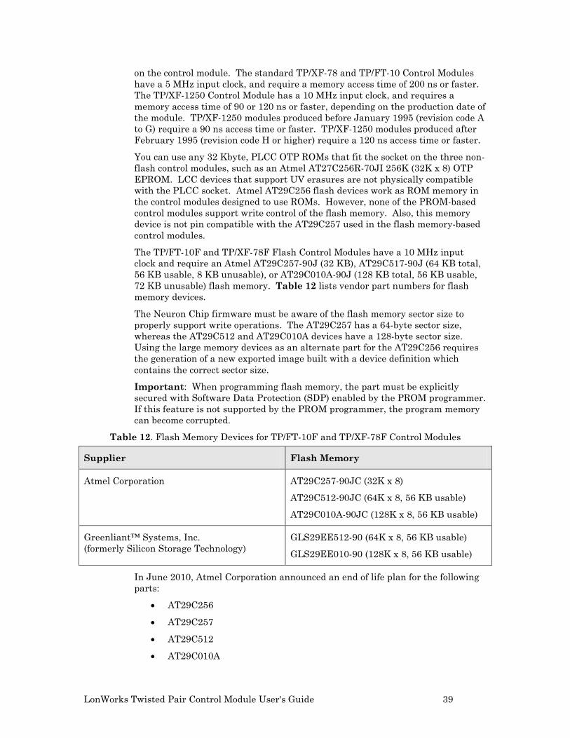
The TP/FT-10F and TP/XF-78F Flash Control Modules have a 10 MHz input clock and require an Atmel AT29C257-90J (32 KB), AT29C517-90J (64 KB total, 56 KB usable, 8 KB unusable), or AT29C010A-90J (128 KB total, 56 KB usable, 72 KB unusable) flash memory. Table 12 lists vendor part numbers for flash memory devices.
The Neuron Chip firmware must be aware of the flash memory sector size to properly support write operations. The AT29C257 has a 64-byte sector size, whereas the AT29C512 and AT29C010A devices have a 128-byte sector size. Using the large memory devices as an alternate part for the AT29C256 requires the generation of a new exported image built with a device definition which contains the correct sector size.
Important: When programming flash memory, the part must be explicitly secured with Software Data Protection (SDP) enabled by the PROM programmer. If this feature is not supported by the PROM programmer, the program memory can become corrupted.
Table 12. Flash Memory Devices for TP/FT-10F and TP/XF-78F Control Modules
Supplier Flash Memory
Atmel Corporation AT29C257-90JC (32K x 8)
AT29C512-90JC (64K x 8, 56 KB usable)
AT29C010A-90JC (128K x 8, 56 KB usable)
Greenliant™ Systems, Inc. (formerly Silicon Storage Technology)
GLS29EE512-90 (64K x 8, 56 KB usable)
GLS29EE010-90 (128K x 8, 56 KB usable)
In June 2010, Atmel Corporation announced an end of life plan for the following parts:
• AT29C256
• AT29C257
• AT29C512
• AT29C010A
40 Programming Considerations
Table 13 lists Greenliant parts that you can use as replacements for obsoleted Atmel parts.
Table 13. Greenliant Replacements for Atmel Parts
Atmel Parallel Flash Part Number
(PLCC32 Package)
Greenliant Parallel Flash Part Number
(PLCC32 Package)
AT29C512-70JU
AT29C512-90JU
GLS29EE512-70-4I-NH
GLS29EE512-70-4I-NHE (Pb free)
AT29C010A-90JI GLS29EE010-70-4I-NHE
Application Program Development and Export Application programs are developed, tested, and debugged using the NodeBuilder FX Development tool; see the NodeBuilder FX User’s Guide for detailed information about developing and testing Neuron C applications. You can also use the Mini FX application for initial device development; see the Mini FX User’s Guide for more information about using the Mini FX application.
In addition, you can develop a ShortStack device with the FT 5000 Control Module; see the ShortStack FX User’s Guide for more information about developing ShortStack devices.
Important: Table 14 lists the minimum required Neuron firmware version for applications built for either of the flash-based Neuron 3150 Control Modules.
Table 14. Neuron Firmware Version Required for Neuron 3150 Control Modules
Name and Model Number Board Number Revision
Minimum Neuron Firmware Version
TP/FT-10F Free Topology Flash Control Module
55020R-10
801-1059-01 Any Any
801-1059-51 xxxxC or earlier Any
801-1059-51 xxxxD or later Version 13.1 or later
TP/XF-78F Flash Control Module
55010R-10
801-1047-01 Any Any
801-1047-51 xxxxB or earlier Any
801-1047-51 xxxxC or later Version 13.1 or later
NodeBuilder FX Development Tool The NodeBuilder FX Development Tool is a hardware and software platform that is used to develop applications for Neuron Chips and Echelon Smart Transceivers. The NodeBuilder tool enables you to do the following tasks:
• View standard resource file definitions for SNVTs, SCPTs, and standard functional profiles.
LonWorks Twisted Pair Control Module User's Guide 41
• Create your own resource files with your UNVTs, UCPTs, and user functional profiles.
• Automatically generate Neuron C code that implements your device interface.
• Edit your Neuron C code to implement your device functionality.
• Compile and build your application, and download it to an Echelon Evaluation Board, Control Module, or to your own devices.
• Test with prototype hardware to test your device’s I/O and related hardware.
• Install your device into a LONWORKS network and test your device interoperating with other LONWORKS devices.
• Use the LNS Plug-in Framework to develop an LNS plug-in for your device.
• Test your LNS plug-in with the LonMaker Integration Tool to ensure that your device is easy to configure and install.
The NodeBuilder FX Development Tool (Service Release 1 or later) is required to build applications for Series 5000 devices.
For more information about using the NodeBuilder FX Development Tool, see the NodeBuilder FX/FT Quick Start and the NodeBuilder FX User’s Guide.
The NodeBuilder FX Development Tool uses device template files to represent target device hardware configuration information. The NodeBuilder Device Template wizard runs during the creation of a new device template. This wizard provides an opportunity to select predefined hardware templates. At a later point in the development process, you can access the hardware template through the Development and Release folders of the project pane.
After you create the hardware template, drag the new hardware template to the device. Drag the newly created icon in the User Templates folder to the Release folder of the device template to complete the procedure.
You can update the user-defined hardware template at any time by double-clicking the template icon. Your new changes affect any projects opened and compiled using this template. A Build All might be required if you change a hardware template without making any other changes.
The following sections describe how to configure the development environment for Neuron 3150 Control Modules and FT 5000 Control Modules.
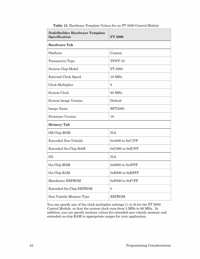
Configuration for FT 5000 Control Modules The NodeBuilder FX Development Tool, Service Release 1 (4.01), does not include hardware templates for the FT 5000 Control Module. However, a future release of the NodeBuilder FX Development Tool will include appropriate hardware templates for the FT 5000 Control Module.
You can use the FT 5000 Evaluation Board hardware template as a base for creating a custom hardware template for the FT 5000 Control Module. Table 15 on page 42 shows the values required for each tab in the NodeBuilder device template editor to support an FT 5000 Control Module. Use this hardware template as a basis for your device development.
42 Programming Considerations
Table 15. Hardware Template Values for an FT 5000 Control Module
NodeBuilder Hardware Template Specification FT 5000
Hardware Tab
Platform Custom
Transceiver Type TP/FT-10
Neuron Chip Model FT 5000
External Clock Speed 10 MHz
Clock Multiplier 8
System Clock 80 MHz
System Image Version Default
Image Name BFT5000
Firmware Version 19
Memory Tab
Off-Chip ROM N/A
Extended Non-Volatile 0x4000 to 0xC7FF
Extended On-Chip RAM 0xC800 to 0xE7FF
I/O N/A
On-Chip ROM 0x0000 to 0x3FFF
On-Chip RAM 0xE800 to 0xEFFF
Mandatory EEPROM 0xF000 to 0xF7FF
Extended On-Chip EEPROM 0
Non-Volatile Memory Type EEPROM
You can specify any of the clock multiplier settings (½ to 8) for the FT 5000 Control Module, so that the system clock runs from 5 MHz to 80 MHz. In addition, you can specify memory values for extended non-volatile memory and extended on-chip RAM to appropriate ranges for your application.
LonWorks Twisted Pair Control Module User's Guide 43
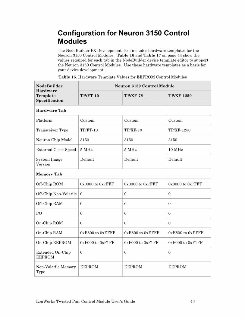
Configuration for Neuron 3150 Control Modules The NodeBuilder FX Development Tool includes hardware templates for the Neuron 3150 Control Modules. Table 16 and Table 17 on page 44 show the values required for each tab in the NodeBuilder device template editor to support the Neuron 3150 Control Modules. Use these hardware templates as a basis for your device development.
Table 16. Hardware Template Values for EEPROM Control Modules
NodeBuilder Hardware Template Specification
Neuron 3150 Control Module
TP/FT-10 TP/XF-78 TP/XF-1250
Hardware Tab
Platform Custom Custom Custom
Transceiver Type TP/FT-10 TP/XF-78 TP/XF-1250
Neuron Chip Model 3150 3150 3150
External Clock Speed 5 MHz 5 MHz 10 MHz
System Image Version
Default Default Default
Memory Tab
Off-Chip ROM 0x0000 to 0x7FFF 0x0000 to 0x7FFF 0x0000 to 0x7FFF
Off-Chip Non-Volatile 0 0 0
Off-Chip RAM 0 0 0
I/O 0 0 0
On-Chip ROM 0 0 0
On-Chip RAM 0xE800 to 0xEFFF 0xE800 to 0xEFFF 0xE800 to 0xEFFF
On-Chip EEPROM 0xF000 to 0xF1FF 0xF000 to 0xF1FF 0xF000 to 0xF1FF
Extended On-Chip EEPROM
0 0 0
Non-Volatile Memory Type
EEPROM EEPROM EEPROM
44 Programming Considerations
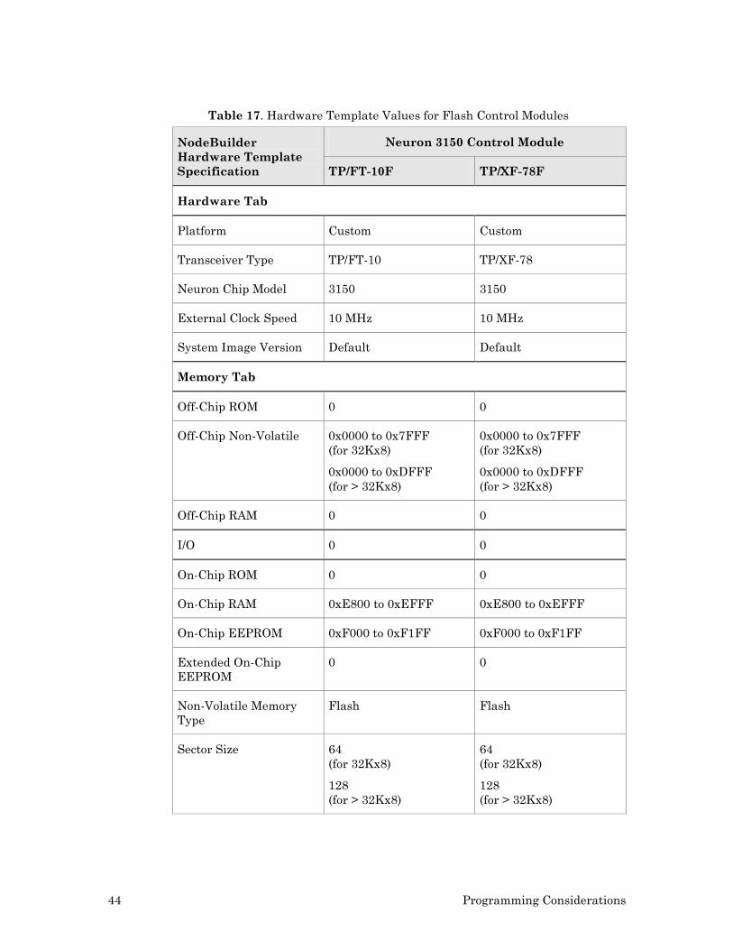
Table 17. Hardware Template Values for Flash Control Modules
NodeBuilder Hardware Template Specification
Neuron 3150 Control Module
TP/FT-10F TP/XF-78F
Hardware Tab
Platform Custom Custom
Transceiver Type TP/FT-10 TP/XF-78
Neuron Chip Model 3150 3150
External Clock Speed 10 MHz 10 MHz
System Image Version Default Default
Memory Tab
Off-Chip ROM 0 0
Off-Chip Non-Volatile 0x0000 to 0x7FFF (for 32Kx8)
0x0000 to 0xDFFF (for > 32Kx8)
0x0000 to 0x7FFF (for 32Kx8)
0x0000 to 0xDFFF (for > 32Kx8)
Off-Chip RAM 0 0
I/O 0 0
On-Chip ROM 0 0
On-Chip RAM 0xE800 to 0xEFFF 0xE800 to 0xEFFF
On-Chip EEPROM 0xF000 to 0xF1FF 0xF000 to 0xF1FF
Extended On-Chip EEPROM
0 0
Non-Volatile Memory Type
Flash Flash
Sector Size 64 (for 32Kx8)
128 (for > 32Kx8)
64 (for 32Kx8)
128 (for > 32Kx8)
LonWorks Twisted Pair Control Module User's Guide 45
Programming The NodeBuilder FX Development Tool generates application image files automatically with each build. After a build is successfully completed using the correct device template file, the next step is to commit the program image to the program memory device using a PROM programmer or an in-circuit programmer. The program images are created in the device directory, with a base file name that matches the device name:
• An FT 5000 Control Module is initially programmed using the serial EEPROM image file (device_name.NME). See Using an Aardvark I2C/SPI Host Adapter on page 36 for information about using the Aardvark I2C/SPI Host Adapter with the Flash Center Memory Programmer software.
• PROM-based devices are programmed using the Neuron ROM image file (device_name.NRI).
• Flash-based control modules are initially programmed using the Neuron EEPROM/Flash image file (device_name.NEI).
Important: When programming flash memory, the part must be explicitly secured with Software Data Protection (SDP) enabled by the PROM programmer. If this feature is not supported by the PROM programmer, the program memory could become corrupted.
Mini FX Evaluation Kit Echelon’s Mini FX Evaluation Kit is a tool for evaluating the development of control network applications with the ISO/IEC 14908-1 (ANSI/CEA-709.1 and EN14908) Control Network Protocol. You can use the Mini FX Evaluation Kit to develop a prototype or production control system that requires networking, particularly in the rapidly growing, price-sensitive mass markets of smart light switches, thermostats, and other simple devices and sensors. You can also use the Mini FX Evaluation Kit to evaluate the development of applications for such control networks using the LONWORKS platform.
The Mini FX Evaluation Kit (or later) is required to build applications for Series 5000 devices.
For more information about using the Mini FX Evaluation Kit, see the Mini FX/FT Quick Start and the Mini FX User’s Guide.
ShortStack FX Developer’s Kit You can use the ShortStack FX Developer’s Kit to develop host-based LONWORKS devices that use the LonTalk® Compact API and a ShortStack Micro Server.
A ShortStack Micro Server is a Series 3100 Smart Transceiver, an FT 5000 Smart Transceiver, or a Neuron 5000 Processor, with firmware that implements layers 2 to 5 (and part of layer 6) of the LonTalk protocol. The host processor implements the application layer (layer 7) and part of the presentation layer (layer 6).
The ShortStack firmware allows you to use almost any host processor for your device’s application and I/O. The Smart Transceiver or Neuron 5000 Processor
46 Programming Considerations
implements layers 2 to 5 (and part of layer 6) of the LonTalk protocol and provides the physical interface for the LONWORKS communications channel.
A simple serial communications interface provides communications between the ShortStack Micro Server and the host processor. Because a ShortStack Micro Server can work with any host processor, you must provide the serial driver implementation, although Echelon does provide the serial driver API and an example driver for a specific host processor. Currently, example drivers are available for an Atmel ARM7 microprocessor and an Altera Nios II embedded processor.
For ShortStack device development, you use the C programming language. You use the Echelon LonTalk Interface Developer utility to create the application framework. Your application uses an ANSI C API, the Echelon LonTalk Compact API, to manage communications with the ShortStack Micro Server and devices on the LONWORKS network.
See the ShortStack FX User’s Guide for more information about the ShortStack Developer’s Kit.

www.echelon.com