low-cost 3d chip stacking with thruchip wireless … grinding, causing impurities affecting device...
TRANSCRIPT

Low-Cost 3D Chip Stacking with
ThruChip Wireless Connections
[email protected] [email protected] [email protected]
ThruChip Communications
August 11, 2014
Hot Chips 26
2 Hot Chips 26 – ThruChip Wireless Connections August 11, 2014
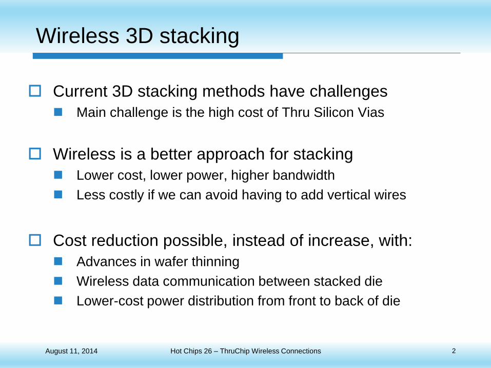
Wireless 3D stacking
Current 3D stacking methods have challenges
Main challenge is the high cost of Thru Silicon Vias
Wireless is a better approach for stacking
Lower cost, lower power, higher bandwidth
Less costly if we can avoid having to add vertical wires
Cost reduction possible, instead of increase, with:
Advances in wafer thinning
Wireless data communication between stacked die
Lower-cost power distribution from front to back of die
3 Hot Chips 26 – ThruChip Wireless Connections August 11, 2014
Challenges with
current 3D stacking

4 Hot Chips 26 – ThruChip Wireless Connections August 11, 2014
3D Stacking with Wire Bonds Staircase stacking
constrains wire bond access
to one side of each die.
spacer
Cons:
High wire bond inductance
Higher power IO
Bandwidth limited to a few GHz
Staircase stacking constraints Limited number of bond wires
Underside clearance limits die thinness
Pros:
Low Cost
Good yield
Allows ~50m thin die
Existing infrastructure

5 Hot Chips 26 – ThruChip Wireless Connections August 11, 2014
3D Stacking with Thru Silicon Vias (TSV)
Cons:
High Cost (1.4x - 2x) over bare die
Requires new CMOS process
Yield reductions from bumps
Area impact from TSV & KOZ
Effects on nearby transistors
Pros:
~10x lower power IO
Thousands of IO possible

6 Hot Chips 26 – ThruChip Wireless Connections August 11, 2014
Proposal for lower cost 3D stacking
Separate Data Communication from Power Distribution
Data Communication: Use wireless near-field inductive coupling
Uses simple CMOS digital circuits: No new semiconductor process expense
Provides best in class inter-die power and bandwidth
May reduce chip cost if IO area can be reduced
Well understood technology validated with dozens of test chips
Becomes more compelling as die get thinner
Power Distribution: Many options available when wireless used for data
Wire bond – Low cost, in high volume production
TAB – Low cost, in high volume production
RDL/FOWLP – Medium cost, production ready
TSV – High cost, early production
Recommend Highly Doped Silicon Vias – New lowest cost proposal, discussed later
7 Hot Chips 26 – ThruChip Wireless Connections August 11, 2014
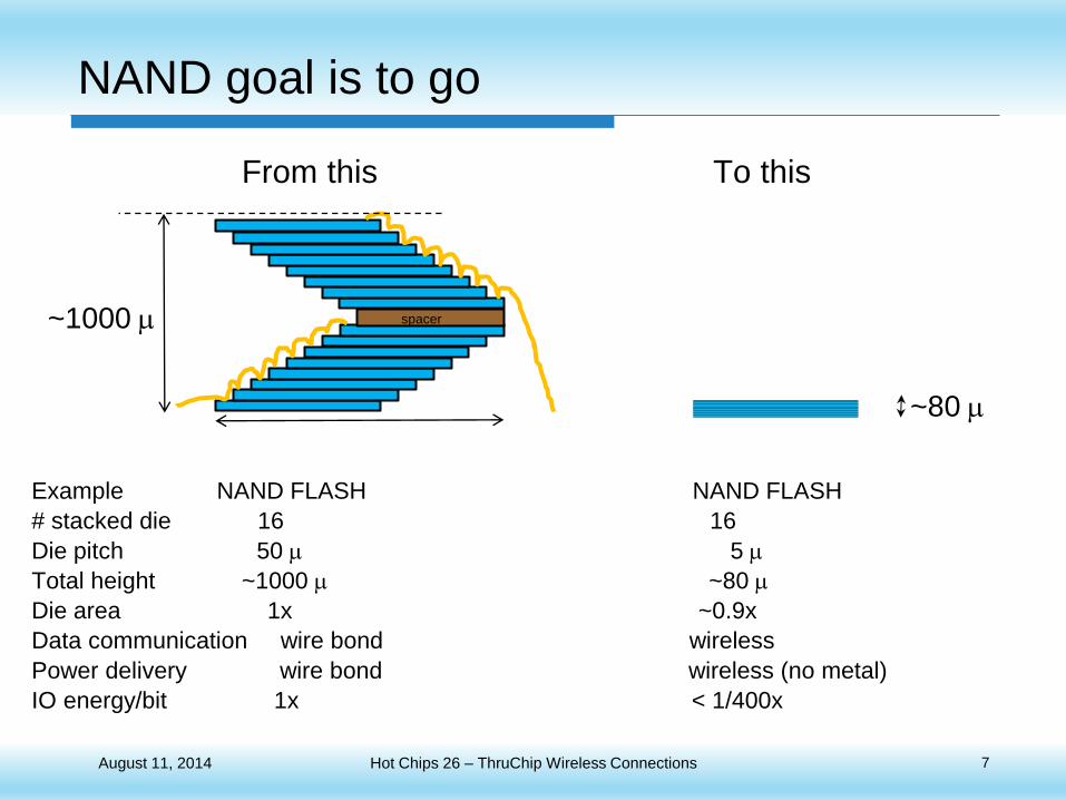
NAND goal is to go
spacer ~1000 m
From this To this
Example NAND FLASH NAND FLASH
# stacked die 16 16
Die pitch 50 m 5 m
Total height ~1000 m ~80 m
Die area 1x ~0.9x
Data communication wire bond wireless
Power delivery wire bond wireless (no metal)
IO energy/bit 1x < 1/400x
~80 m

8 Hot Chips 26 – ThruChip Wireless Connections August 11, 2014
DRAM goal is to go
~275 m
From this To this
Example DRAM with TSV DRAM
# stacked die 5 5
Die pitch 55m 8m
Total height ~275m ~40m
Die area 1x 0.87x
Data communication TSV wireless
Power delivery TSV wireless (no metal vias)
IO energy/bit 1x < 1/10x
~40 m
DRAM die
DRAM die
DRAM die
DRAM die
Base logic die

9 Hot Chips 26 – ThruChip Wireless Connections August 11, 2014
Relevant advances
in wafer thinning

10 Hot Chips 26 – ThruChip Wireless Connections August 11, 2014
Ultra-Thin 4m wafer breakthrough
Wafer thinning has been stuck at ~40m due to “Gettering problem”
Barrier was due in part to loss of the “gettering effect” at smaller dimensions when performing
back grinding, causing impurities affecting device performance (particularly leakage) and yield.
DISCO Corporation solution can now thin to a few microns
DISCO introduced a “Gettering Dry Polish” wheel which forms gettering sites while grinding,
allowing thinning of wafer silicon to a few microns without device damage. [35]
Example: DRAM silicon thinned to 4 microns
See “Ultra Thinning down to 4mm using 300-mm Wafer proven by 40-nm Node 2 Gb DRAM for
3D Multi-stack WOW Applications.”[36] They concluded “No degradation in terms of retention
characteristics and distribution employing 2 Gb DRAM wafer was found after ultra-thinning.”
Ultra-thin wafers can be handled (from DISCO website) [Reference 36]
2Gb DRAM thinned to 4 microns

11 Hot Chips 26 – ThruChip Wireless Connections August 11, 2014
Wireless 3D data

12 Hot Chips 26 – ThruChip Wireless Connections August 11, 2014
Wireless Near-Field Inductive Coupling
Chip designers often spend a lot of time making sure they do not
have too much coupling between adjacent wires.
Idea: Turn that coupling into an advantage.
Use Inductive Coupling for 3D wireless data communication
Inductive coils made with a few turns in standard metal layers
Coil diameter is about 3x the communication distance
Coils communicate vertically to adjacent chips by magnetic field
Receive and transmit coils can be placed concentrically on each die
to form a transceiver
Multiple coils used to increased bandwidth
Bandwidth improves with Moore’s law improvement in devices

13 Hot Chips 26 – ThruChip Wireless Connections August 11, 2014
Receiver
Coil
Communication is via magnetic field
Magnetic field can pass through silicon, including over active circuitry.
dIT
dt VR=k LTLR
Can easily induce a 200 mV
signal in receiver coil.

14 Hot Chips 26 – ThruChip Wireless Connections August 11, 2014
ThruChip Interface (TCI)
Txd
ata
Time
I T
VR
R
xd
ata
Rxdata
Txdata Txdata
Rxdata
Simple transmitter and receiver circuits (basic form shown)
Standard digital CMOS: Scales with Moore’s Law
Bandwidth: >40 Gigabits/second/coil with modern digital CMOS
Delay: About 7 equivalent logic gates (NAND2 FO4)
Energy: About 80 equivalent gates
Chip 1
Chip n
TCI Transmitter
TCI Receiver
Transmitter Coil
Receiver Coil

15 Hot Chips 26 – ThruChip Wireless Connections August 11, 2014
TCI coil example
3 chips with staircase stacking TCI Wireless Transceiver
200 m
4 turns xmitter
4 turns receiver

16 Hot Chips 26 – ThruChip Wireless Connections August 11, 2014
5
10
15
20
25
30
35
64 100 150
Communication Distance, Z [mm]
Usa
ble
Co
il B
an
dw
idth
[G
b/s
] U
sab
le c
ircu
it b
an
dw
idth
de
pe
nd
s o
n d
evic
e
40
45
50
55
60
65
70
75
TCI bandwidth vs communication distance
9 die stacking
D=200m
Z=64m
D=200m
D=300m D=400m D=500m
D=100m
Usable BW of 28 Gbps
5-die stacking
D=100m
Z=32m Usable BW of 66 Gbps
32
Coil diameter D=3 x Z
Assumes 8m die pitch

17 Hot Chips 26 – ThruChip Wireless Connections August 11, 2014
Data from references [16,25,28]
High BW: Data rate is equivalent to 1.5x of 5-stage ring oscillator
Fast: Delay is equivalent to 7x of 2NAND FO4
Low Power: Energy is equivalent to 80x of 2NAND FO4
Small: Circuit layout area is equivalent to 36x 2NAND
10
100
1000
10000
Dela
y [
ps]
180 90 45 32
Process [nm CMOS]
1 65
7x
0.01
0.1
1
10
En
erg
y D
issip
atio
n [p
J/b
]
180 90 45 32
Process [nm CMOS]
0.001 65
80x
1
10
100
180 90 45 32
Process [nm CMOS]
65
Da
ta R
ate
, F
req
ue
ncy [G
b/s
]
1.5x
TCI scales with digital CMOS
=Measured silicon data =Simulated data

18 Hot Chips 26 – ThruChip Wireless Connections August 11, 2014
Tra
nsm
issio
n p
ow
er, d
ela
y
Number of Stacked Chips
TSV
TCI
Chip4
IO
Chip3
Chip2
Chip1
Interface
TSV TCI
Tx Rx
Tx Rx
Tx Rx
Tx Rx
Tx Rx
IO
IO
IO
IO
ESD
TSV
TCI broadcasting more efficient than TSV
TSV power and delay is increased in proportion to # of stacked chips. TCI transmitter consumes constant power and delay.
19 Hot Chips 26 – ThruChip Wireless Connections August 11, 2014
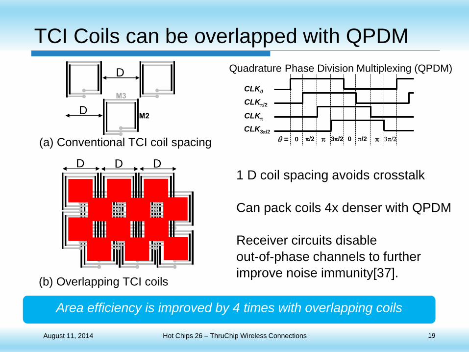
Quadrature Phase Division Multiplexing (QPDM)
(a) Conventional TCI coil spacing
(b) Overlapping TCI coils
q = p/2 p 3p/2 0 p/2 p 3p/2 0
CLK0
CLKp/2
CLKp
CLK3p/2
TCI Coils can be overlapped with QPDM
Area efficiency is improved by 4 times with overlapping coils
1 D coil spacing avoids crosstalk
Can pack coils 4x denser with QPDM
Receiver circuits disable
out-of-phase channels to further
improve noise immunity[37].
D D D
D
D
20 Hot Chips 26 – ThruChip Wireless Connections August 11, 2014
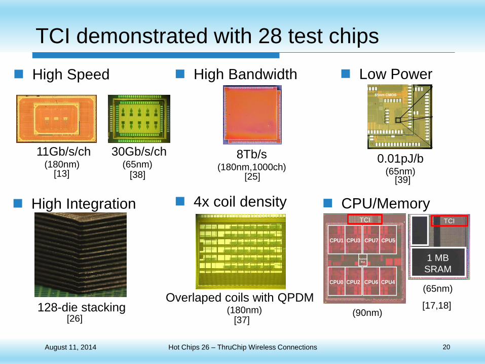
TCI demonstrated with 28 test chips
128-die stacking
High Integration
11Gb/s/ch (180nm)
8Tb/s (180nm,1000ch)
30Gb/s/ch (65nm)
High Speed
0.01pJ/b (65nm)
Low Power
CPU/Memory
4x coil density
Overlaped coils with QPDM
CPU2CPU0 CPU4CPU6
CPU3CPU1 CPU5CPU7
System
Bus
CPU2CPU0 CPU4CPU6
CPU3CPU1 CPU5CPU7
System
Bus
TCI
1 MB
SRAM
TCI
High Bandwidth
[26] [37]
[17,18]
[25] [39] [13] [38]
(90nm)
(65nm)
(180nm)

21 Hot Chips 26 – ThruChip Wireless Connections August 11, 2014
ThruChip introduces
Highly Doped Silicon Vias (HDSV)
for “Wireless” Power Delivery
22 Hot Chips 26 – ThruChip Wireless Connections August 11, 2014
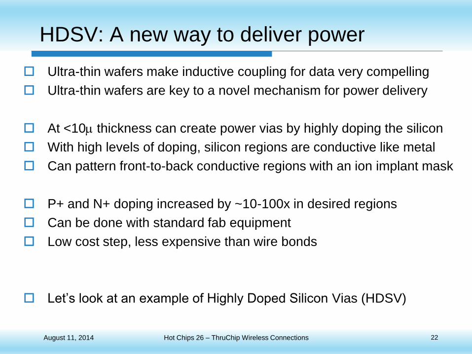
HDSV: A new way to deliver power
Ultra-thin wafers make inductive coupling for data very compelling
Ultra-thin wafers are key to a novel mechanism for power delivery
At <10m thickness can create power vias by highly doping the silicon
With high levels of doping, silicon regions are conductive like metal
Can pattern front-to-back conductive regions with an ion implant mask
P+ and N+ doping increased by ~10-100x in desired regions
Can be done with standard fab equipment
Low cost step, less expensive than wire bonds
Let’s look at an example of Highly Doped Silicon Vias (HDSV)

23 Hot Chips 26 – ThruChip Wireless Connections August 11, 2014
Start with standard wafer
~700 m
Then add transistors and metal normally, metal caps on HDSV Thin silicon to ~4 microns
~4 m
Add implants to create highly doped regions for power vias
Highly Doped Silicon Vias for power distribution
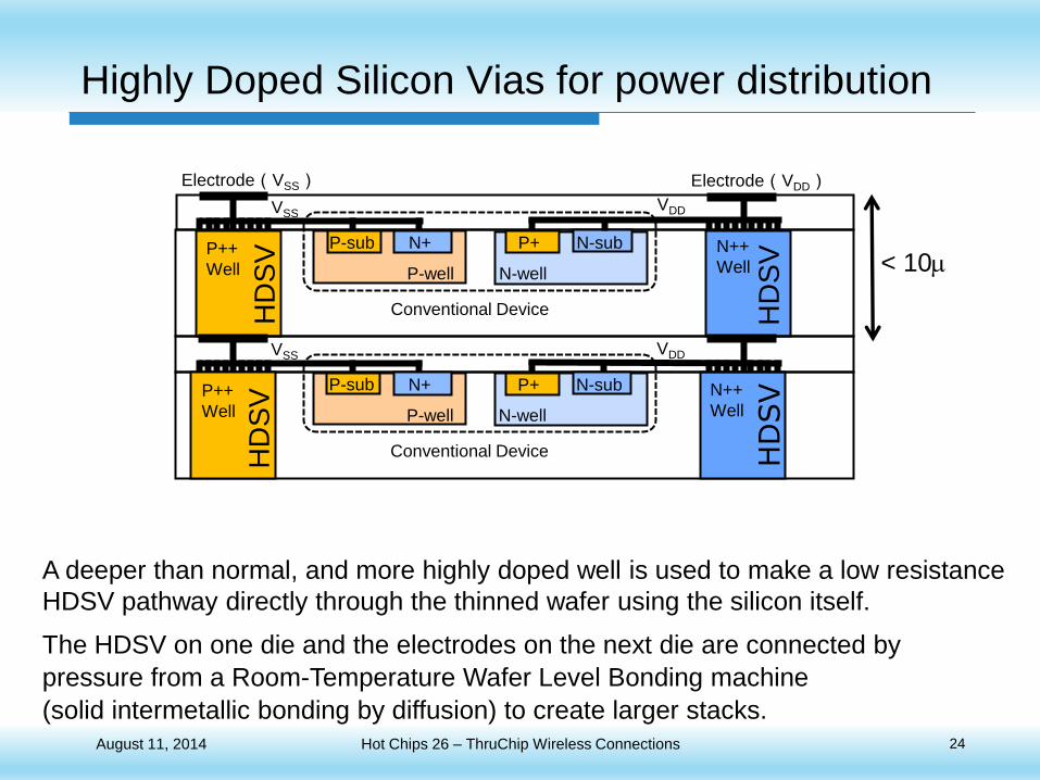
24 Hot Chips 26 – ThruChip Wireless Connections August 11, 2014
Highly Doped Silicon Vias for power distribution
A deeper than normal, and more highly doped well is used to make a low resistance
HDSV pathway directly through the thinned wafer using the silicon itself.
VDD VSS
P-sub N+ N-sub P+
N-well
Conventional Device
P-well < 10m H
DS
V
P++
Well N++
Well
HD
SV
The HDSV on one die and the electrodes on the next die are connected by
pressure from a Room-Temperature Wafer Level Bonding machine
(solid intermetallic bonding by diffusion) to create larger stacks.
Electrode(VSS) Electrode(VDD)
VDD VSS
P++
Well N++
Well
P-sub N+ N-sub P+
N-well
Conventional Device
P-well
HD
SV
HD
SV

25 Hot Chips 26 – ThruChip Wireless Connections August 11, 2014
Electrode(VSS)
VDD VSS
P-sub N+ N-sub P+
N-well
Conventional Device
P-well
VDD VSS
P-sub N+ N-sub P+
N-well
Conventional Device
P-well
Electrode(VDD)
VDD VSS
P-sub N+ N-sub P+
N-well
Conventional Device
P-well
Ground Power
Highly Doped Silicon Vias for power distribution
HD
SV
HD
SV
HD
SV
HD
SV
HD
SV
HD
SV
26 Hot Chips 26 – ThruChip Wireless Connections August 11, 2014
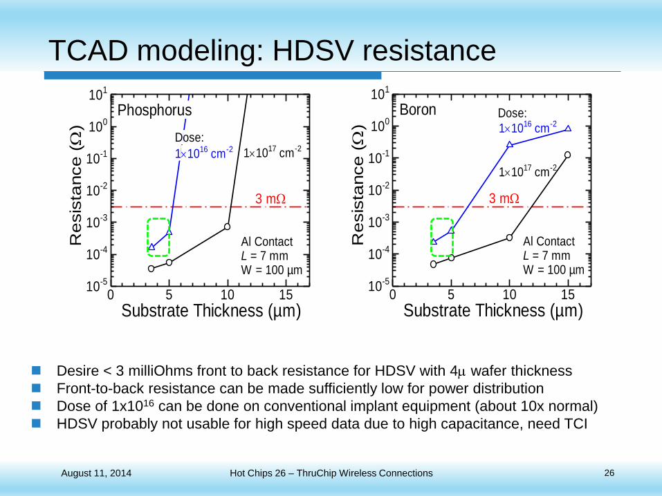
TCAD modeling: HDSV resistance
Desire < 3 milliOhms front to back resistance for HDSV with 4m wafer thickness
Front-to-back resistance can be made sufficiently low for power distribution
Dose of 1x10¹⁶ can be done on conventional implant equipment (about 10x normal)
HDSV probably not usable for high speed data due to high capacitance, need TCI
Substrate Thickness (µm)
Re
sis
tance
(
)
Phosphorus
11016 cm-2
Top Oxide: 10 nmImplantation Energy: 200 keVAnnealing Temp.: 1050 Deg. Time: 50 h
3 m
Al ContactL = 7 mmW = 100 µm
11017 cm-2Dose:
0 5 10 1510-5
10-4
10-3
10-2
10-1
100
101
Substrate Thickness (µm)
Re
sis
tance
(
)
Boron11016 cm-2
Top Oxide: 10 nmImplantation Energy: 200 keVAnnealing Temp.: 1050 Deg. Time: 50 h
3 m
Al ContactL = 7 mmW = 100 µm
11017 cm-2
Dose:
0 5 10 1510-5
10-4
10-3
10-2
10-1
100
101
27 Hot Chips 26 – ThruChip Wireless Connections August 11, 2014
HDSV Wireless Power Distribution
No metallic TSV’s, no wire bonds, no solder bumps
Just stack chips and connect the stack to power
Very loose alignment requirements on both data and power
Data transmitted wirelessly with near field inductive coupling
Power and ground go directly through the silicon, by using high levels of
doping on ultra-thin die.
Since silicon provides the power conduits instead of “metal wires”, the
power distribution is “wireless” ;-)
HDSV should be low cost, extra implants are the only change to chips
28 Hot Chips 26 – ThruChip Wireless Connections August 11, 2014
Comparison Example
Stacked HBM DRAM
TSV vs TCI/HDSV

29 Hot Chips 26 – ThruChip Wireless Connections August 11, 2014
Example HBM DRAM with TSV 6.91 mm
5.1
mm
TSV’s provide 8 channels of independent 128-bit I/O
Total of 1024 TSV I/O at 1 Gbps for 128 GB/s
This is a simplified
hypothetical example
using Hynix HBM as
a point of comparison
for stacking 5 die.
~ 18% of die area
dedicated to TSV IO
30 Hot Chips 26 – ThruChip Wireless Connections August 11, 2014
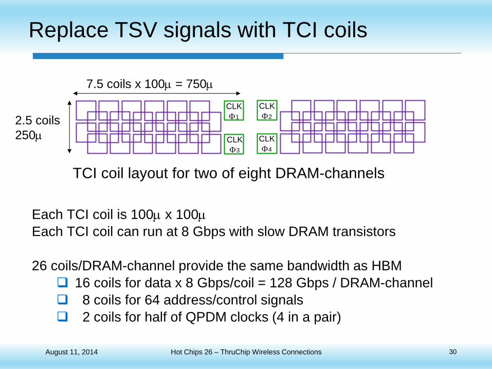
Replace TSV signals with TCI coils
7.5 coils x 100m = 750m
2.5 coils
250m
TCI coil layout for two of eight DRAM-channels
CLK
F1
CLK
F2
CLK
F3
CLK
F4
Each TCI coil is 100m x 100m
Each TCI coil can run at 8 Gbps with slow DRAM transistors
26 coils/DRAM-channel provide the same bandwidth as HBM
16 coils for data x 8 Gbps/coil = 128 Gbps / DRAM-channel
8 coils for 64 address/control signals
2 coils for half of QPDM clocks (4 in a pair)
31 Hot Chips 26 – ThruChip Wireless Connections August 11, 2014
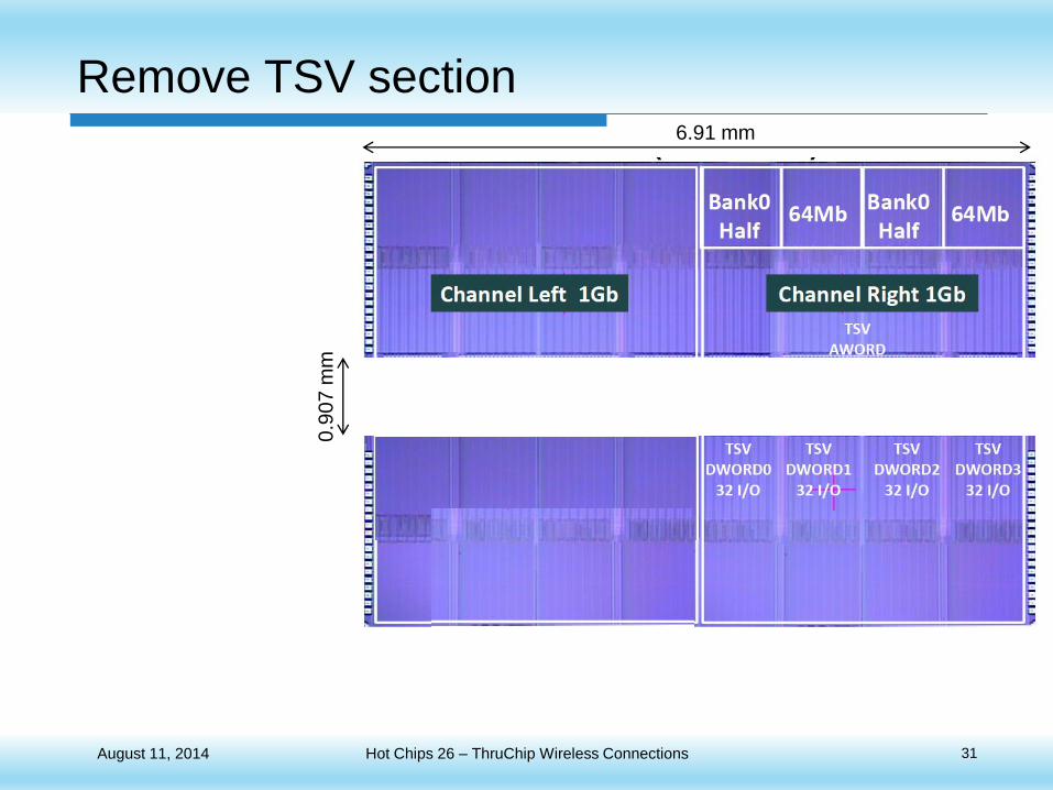
Remove TSV section
0.9
07 m
m
6.91 mm
32 Hot Chips 26 – ThruChip Wireless Connections August 11, 2014
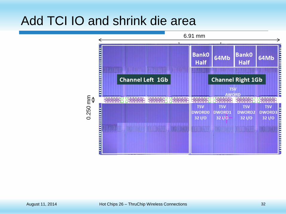
Add TCI IO and shrink die area
0.2
50 m
m
6.91 mm

33 Hot Chips 26 – ThruChip Wireless Connections August 11, 2014
Define Power/Ground with HDSV
Vss
Vdd
These are the mask patterns for low resistance implants
for HDSV conduits from the front to back side of each die.
34 Hot Chips 26 – ThruChip Wireless Connections August 11, 2014
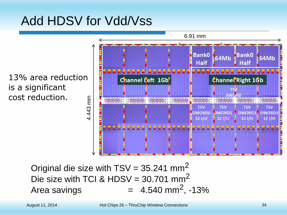
Add HDSV for Vdd/Vss
4.4
43 m
m
6.91 mm
Original die size with TSV = 35.241 mm2
Die size with TCI & HDSV = 30.701 mm2
Area savings = 4.540 mm2, -13%
13% area reduction
is a significant
cost reduction.

35 Hot Chips 26 – ThruChip Wireless Connections August 11, 2014
Final stack DRAM example
~40 m Base die (face down)
HBM DRAM with TCI
HBM DRAM with TCI
HBM DRAM with TCI
HBM DRAM with TCI
Assumptions:
• Each die 8m thick, 4m silicon and 4m metal stack.
• Data sent wirelessly with TCI inductive coupling links.
• Power passes through existing silicon with Highly Doped Silicon Vias.
• Base die can translate to standard IO or TCI link to a SoC.
• Smaller die size provides significant cost reduction.
• Cost of implants for HDSV and circuits for TCI relatively negligible.
• Seems likely this will result in a net cost reduction when using this stacking approach.
• No vertical metal wires! Wireless 3D stacking.
Vss in H
DS
V
Vd
d in H
DS
V
Vd
d in H
DS
V
Vss in H
DS
V
TC
I C
ha
nn
els

36 Hot Chips 26 – ThruChip Wireless Connections August 11, 2014
Summary
The synergy of ultra die thinning, TCI wireless data communication
and Highly Doped Silicon Vias for power provides a future path for
cost reduction using 3D stacking.
Wireless TCI near-field inductive coupling has been well proven with
28 silicon test chips.
Power distribution when using TCI can be done with proven
techniques such as wire bond, TAB or even TSV.
Power distribution for TCI with Highly Doped Silicon Vias is a new
and still untested technique, which offers great promise for lowering
3D stacking costs. Help us make it happen.

37 Hot Chips 26 – ThruChip Wireless Connections August 11, 2014
[01] D. Mizoguchi, et al., “A 1.2Gb/s/pin Wireless Superconnect Based on Inductive Inter-chip Signaling (IIS),” ISSCC, pp.142-143, Feb. 2004.
[02] N. Miura, et al., “Analysis and Design of Inductive Coupling and Transceiver Circuit for Inductive Inter-Chip Wireless Superconnect,” Symp. VLSI Circuits, pp. 246-249, Jun. 2004.
[03] N. Miura, et al., “Cross Talk Countermeasures in Inductive Inter-Chip Wireless Superconnect,” CICC, pp.99-102, Oct. 2004.
[04] N. Miura, et al., “A 195Gb/s 1.2W 3D-Stacked Inductive Inter-Chip Wireless Superconnect with Transmit Power Control Scheme,” ISSCC, pp.264-265, Feb. 2005.
[05] D. Mizoguchi, et al., "Measurement of Inductive Coupling in Wireless Superconnect,” SSDM, pp.670-671, Sep. 2005.
[06] N. Miura, et al., “A 1Tb/s 3W Inductive-Coupling Transceiver for Inter-Chip Clock and Data Link,” ISSCC, pp.424-425, Feb. 2006.
[07] T. Kuroda, et al., “Perspective of Low-Power and High-Speed Wireless Inter-Chip Communications for SiP Integration,” ESSCIRC, pp.3-6, Sep. 2006.
[08] D. Mizoguchi, et al., “Constant Magnetic Field Scaling in Inductive-Coupling Data Link,” SSDM, pp. 606–607, Sep. 2006.
[09] N. Miura, et al., “A 0.14pJ/b Inductive-Coupling Inter-Chip Data Transceiver with Digitally-Controlled Precise Pulse Shaping,” ISSCC, pp.264-265, Feb. 2007.
[10] T. Kuroda, “CMOS Proximity Wireless Communications for SiP Integration (Invited),” ISSCC, Feb. 2007.
[11] T. Kuroda, “Low power technology for system LSI,” J. IEICE, vol. 90, no. 11, pp. 977-981, Nov. 2007.
[12] K. Niitsu, et al., “Interference from Power/Signal Lines and to SRAM Circuits in 65nm CMOS Inductive-Coupling Link,” A-SSCC, pp.131-134, Nov. 2007.
[13] N. Miura, et al., “An 11Gb/s Inductive-Coupling Link with Burst Transmission,” ISSCC, pp.298-299, Feb. 2008.
[14] D. Mizoguchi, et al., “Constant Magnetic Field Scaling in Inductive-Coupling Data Link,” IEICE Trans. Electronics, Vol. E91-C, No. 2, pp. 200- 205, Feb. 2008.
[15] K. Niitsu, et al., “Misalignment Tolerance in Inductive-Coupling Inter-Chip Link for 3D System Integration,” SSDM, pp.86-87, Sep. 2008.
[16] Y. Sugimori, et al., “A 2Gb/s 15pJ/b/chip Inductive-Coupling Programmable Bus for NAND Flash Memory Stacking,” ISSCC, pp.244-245, Feb. 2009.
[17] K. Niitsu, et al., “An Inductive-Coupling Link for 3D Integration of a 90nm CMOS Processor and a 65nm CMOS SRAM,” ISSCC, pp.480-481, Feb. 2009.
[18] K. Osada, et al., “3D System Integration of Processor and Multi-Stacked SRAMs by Using Inductive-Coupling Links,” Symp on VLSI Circuits, pp. 256-257, Jun. 2009.
[19] Y. Kohama, et al., “A Scalable 3D Processor by Homogeneous Chip Stacking with Inductive-Coupling Link,” Symposium on VLSI Circuits, pp. 94-95, Jun. 2009.
[20] S. Kawai, et al., “A 4.7Gb/s Inductive Coupling Interposer with Dual Mode Modem,” Symposium on VLSI Circuits, pp. 92-93, Jun. 2009.
[21] M. Saito, et al., “47% Power Reduction and 91% Area Reduction in Inductive-Coupling Programmable Bus for NAND Flash Memory Stacking,” CICC, pp. 449-452, Sep. 2009.
[22] K. Kasuga, et al., “Electromagnetic Interference and Susceptibility in Inductive-Coupling Link,” SSDM, pp.62-63, Nov. 2009.
[23] M. Saito, et al., “ An Extended XY Coil for Noise Reduction in Inductive-coupling Link,” A-SSCC, pp.305-308, Nov. 2009.
[24] K. Kasuga, et al., “A Wafer Test Method of Inductive-Coupling Link,” A-SSCC, pp.301-304, Nov. 2009.
[25] N. Miura, et al., “An 8Tb/s 1pJ/b 0.8mm2/Tb/s QDR Inductive-Coupling Interface Between 65nm CMOS and 0.1um DRAM,” ISSCC, pp.436-437, Feb. 2010.
[26] M. Saito, et al., “A 2Gb/s 1.8pJ/b/chip Inductive-Coupling Through-Chip Bus for 128-Die NAND-Flash Memory Stacking,” ISSCC, pp.440-441, Feb. 2010.
[27] T. Kuroda, “Inductively Coupled ThruChip Interface,” ISSCC, ES3(Energy-Efficient High-Speed Interfaces), Feb. 2010.
[28] N. Miura, et al., “A 0.7V 20fJ/bit Inductive-Coupling Data Link with Dual-Coil Transmission Scheme,” Symposium on VLSI Circuits, pp. 201-202, June 2010.
[29] T. Kuroda, et al., “ThruChip Interface (TCI) for 3D Integration of Low-Power System (Invited),” IEDM, p.17.1.1, Dec. 2010.
[30] N. Miura, et al., “A 2.7Gb/s/mm2 0.9pJ/b/Chip 1Coil/Channel ThruChip Interface for NAND Flash Memory Stacking,” ISSCC, pp.490-491, Feb. 2011.
[31] Y. Shimazaki, et al., “A 5Gbps/ch ThruChip Interface and Autom. P&R Design Methodology for 3-D Integration of 45nm CMOS Processors,” COOL Chips XV, pp.1-3, Apr. 2012.
[32] Y. Koizumi, et al., “Dynamic power control with a heterogeneous multi-core system using a 3-D wireless inductive coupling interconnect,” ICFPT'12, pp. 293-296, Dec. 2012.
[33] H. Matsutani, et al., “A Case for Wireless 3D NoCs for CMPs ,” ASP-DAC'13, pp. 23-28, Jan. 2013.
[34] Y. Take, et al., “3D Clock Distribution Using Vertically/Horizontally Coupled Resonators ,” ISSCC, pp. 258-259, Feb. 2013.
[35] “Introduction of Gettering DP Wheel”, DISCO Website, in both English and Japanese, http://www.disco.co.jp/jp/solution/apexp/polisher/gettering.html
[36] Y.S. Kim, et al., “Ultra Thinning down to 4mm using 300-mm Wafer proven by 40-nm Node 2 Gb DRAM for 3D Multi-stack WOW Applications”, Symp. VLSI Circuits, pp. 22-23, June 2014.
[37] A.R. Junaidi, Y. Take, T. Kuroda, “A 352 Gb/s Inductive-Coupling DRAM/SoC Interfaces Using Overlapping Coils with Phase Division Multiplexing and Ultra-Thin Fan-Out Wafer Level Package”, Symp.
VLSI Circuits, June 2014.
[38] Y. Take, N. Miura, T. Kuroda, “A 30 Gb/s/Link 2.2 Tb/s/mm2 Inductively-Coupled Injection-Locking CDR for High-Speed DRAM Interface”, JSSC, pp 2552-2559, November 2011.
[39] N. Miura, e al., A 0.55V 10fJ/bit Inductive-Coupling Data Link and 0.7V 135fJ/Cycle Clock Link with Dual-Coil Transmission Scheme”, IEEE JSSC, pp. 965-973, April 2011.
References