low frequency response high frequency response miller ... · amplifier: frequency response bode...
TRANSCRIPT
Am
plifier: Frequency Response
Bode plot
Miller effect
High frequency response
Low frequency response
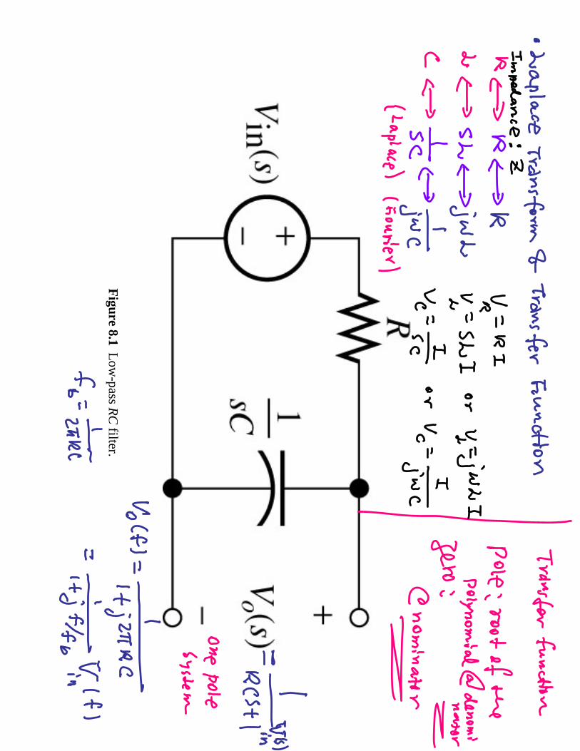
Figure 8.1 Low-pass RC
filter.

Figure 8.2 Logarithmic frequency scale.

Figure 8.3 Bode plot for the low
-pass RCfilter.

Figure 8.4 Bode plot for phase of the low
-pass RCfilter.

Figure 8.5 Circuit for Exam
ple 8.1.

Figure 8.6 Bode plots of the term
s on the right-hand side of Equation (8.19).
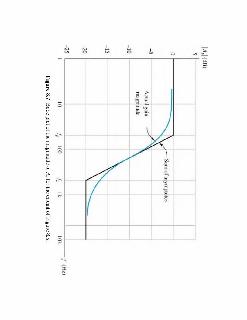
Figure 8.7 Bode plot of the m
agnitude of Av for the circuit of Figure 8.5.

Figure 8.8 Approxim
ate plots of the terms of Equation (8.20).

Figure 8.9 Bode phase plot of the voltage-transfer function for the circuit of Figure 8.5.

High-frequency FET equivalent circuit.
High frequency FET m
odel with
parasitic capacitances•
Small signal m
odel should include the parasitic capacitances of the device to determ
ine the frequency response.

Com
mon-source am
plifier.
•W
e can draw the sm
all signal equivalent circuit for the com
mon source am
plifier given below
.

Small-signal equivalent circuit of the com
mon-source am
plifier.
•U
sing same node equations as before, w
e can find the transfer function from
input to output.
•The transfer function w
ill contain poles and zeros due to the parasitic capacitances show
n.

Bode plot of voltage gain for a typical com
mon-source stage.
•C
ombined response of individual poles and
zeros would determ
ine the overall frequency response of the am
plifier.


A feedback im
pedance can be replaced by impedances in parallel w
ith the input and output terminals.
•An im
pedance Zfconnected from the input of an
amplifier to the output can be replaced by an
impedance
across the input terminals and im
pedance across the output term
inals (next).
v
fM
illerin
AZ
Z−
=1
,
1.
,−
=v
vf
Miller
outA
AZ
Z

A feedback im
pedance can be replaced by impedances in parallel w
ith the input and output terminals.

Miller Effect Applied to Feedback
Capacitance
•M
iller theorem proves very useful since it is
much easier to determ
ine poles and zeros by splitting the C
gd.•
Cgd
will reflect to input side as C
Miller = (1-
Av)Cgd (next).
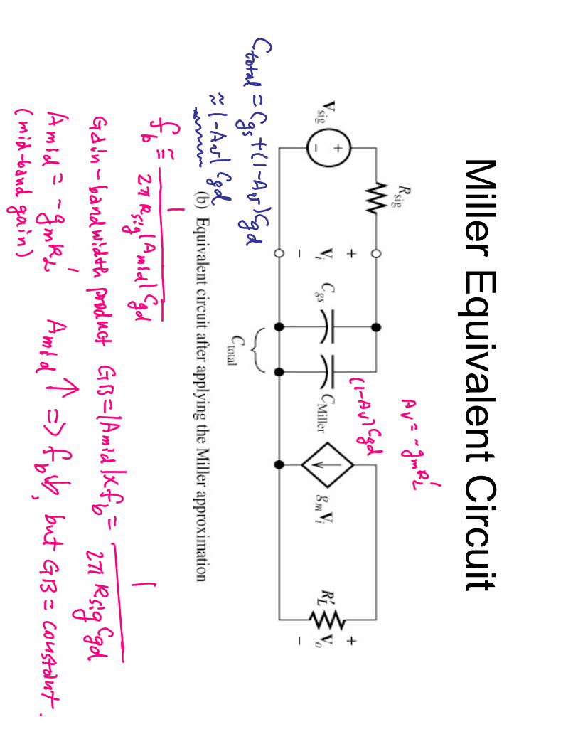
Miller E
quivalent Circuit

The rp –b
model for the B
JT.
The rπ -βm
odel

Com
mon-em
itter h-parameter sm
all-signal equivalent circuit. (Note:h
ie is resistance And h
oe is conductance).
The two-port hybrid m
odel

Hybrid-p
equivalent circuit.
The hybrid-πequivalent circuit
•The resistance rx is called base-spreading resistance and accounts for the ohm
icresistance of the base
region.•
The resistance rµ accounts for the effect of base-w
idth modulation on the input characteristic.
•C
µ is the depletion capacitance of base-collector junction and C
πis base-em
itter diffusion capacitance. •
The transition frequency (unity current gain frequency) can be w
ritten as; )
(2
πµ
ππ
βC
Cr
ft+
=