low power digital design fundamental - high-speed … chin-chi teng (corporate vp – r&d),...
TRANSCRIPT

Confidential
Chin-Chi Teng (Corporate VP – R&D), Richard Chou (R&D Architect)
Cadence Design System, Inc.
April, 2017
Low Power Digital Design Fundamental

© 2017 Cadence Design Systems, Inc. All rights reserved.
Network/Data Center
Power Efficiency
Total Cost of Ownership
Reliability
Green
Low Power Design Issues Impact ProfitabilityDifferent drivers in different verticals
2
Consumer/Digital Home
Unit Cost (chip package)
Unit Cost (fans etc.)
Reliability
Mobile/Hand-held
Battery Life
Unit Cost (chip package)
Low power requirements drive different design decisions:• Product design architecture and integration decisions
• IP make versus reuse versus buy decisions• Manufacturing process decisions

3 © 2017 Cadence Design Systems, Inc. Cadence confidential. Internal use only.
Agenda
Types of Power Consumption
Low Power Design Methodologies
Low Power Physical Implementation
Advanced Low Power Techniques
Devices – Now & Future
Summary

4 © 2017 Cadence Design Systems, Inc. Cadence confidential. Internal use only.
Types of Power Consumption

April 5, 2017 Cadence Confidential: Cadence Internal Use Only5
Device Current Components
CLIsw
GND
Ile
Ile
Isc
Vin Vout
Vdd
• Dynamic Switching Power– Due to charge/discharge of load cap
– Isw ~ CL Vdd2
• Dynamic Short-circuit Power– Due to direct current path from Vdd to
ground during output switching
– Isc ~ input_slew / CL
• Static Leakage Power– Due to subthreshold & gate leakage
– Ile ~ K*eVgs/T(1-e-Vds/T)
Ptotal = CL.VDD2.fclk .a0�1 + VDD . Ishort-circuit + VDD . Ileakage

April 5, 2017 Cadence Confidential: Cadence Internal Use Only6
Types of Power Consumption
• Dynamic (switching) power consumption
• Short circuit power consumption
• Static (leakage) power consumption
Biggest reason for design failure: Leakage
(So
urc
e IB
S)
REASONS FOR DESIGN RE-SPINS (45nm/40nm)

7 © 2017 Cadence Design Systems, Inc. Cadence confidential. Internal use only.
Low Power Design Methodologies

8 © 2017 Cadence Design Systems, Inc. Cadence confidential. Internal use only.
Low-Power Solution (Cadence)
System Level
• Stratus™ High-Level Synthesis (HLS)
• Palladium® Dynamic Power Analysis (DPA)
• Chip-package co-design with Sigrity™ and Voltus™ solutions
Func. Verification
• Xcelium® Simulator
• Palladium emulator
• JasperGold® Formal Power App
• Analog Mixed-Signal Designer
Synthesis and DFT
• Genus™ Logic Synthesis
• Modus DFT and ATPG
• Conformal Low Power
• Joules RTL Power Estimation
P&R, MS & Signoff
• Innovus™ Implementation System
• OA-based Mixed Signalwith Virtuoso® technology
• MS static checks with Conformal® LP
• Tempus ECO
• Voltus IC Power Integrity Solution
IP
• Energy-efficient Xtensa® cores
• LPDDR, PCI Express® (PCIe®), Ethernet, MIPI, USB, eMMC
• Analog mixed-signal IP including ADC/DAC, AFE, SerDes, PVT Monitors, and power management IP

9 © 2017 Cadence Design Systems, Inc. Cadence confidential. Internal use only.
ROI on Power Optimization at Various Levels
Application
Software
PhysicalDesign
RTL
Cell/IP/MemCircuit
Architecture
Advanced Device/Material
>= 10x
1x – 10x
20% - 1x
10% – 20%
5% – 10%
(Revolutionary!)
<= 5%

10 © 2017 Cadence Design Systems, Inc. Cadence confidential. Internal use only.
Low Power Physical Implementation

April 5, 2017 Cadence Confidential: Cadence Internal Use Only11
The Need for Power Intent Information
LibrariesIP
LogicInformation
(Verilog)
Synthesis
Test
SVP
FormalAnalysis
Simulation
ParserParser
Parser
Logic is “Connected”
P+R
Parser
Pars
er
Pars
er
Hardware
Parser
EquivalenceChecking
Parser
Management
Parser
Power is “Connected”
LibrariesIP
Synthesis
Test
SVP
FormalAnalysis
Simulation
ParserParser
Parser
P+R
Parser
Pars
er
Pars
er
Hardware
Parser
EquivalenceChecking
Parser
Management
Parser
PowerIntent

12 © 2017 Cadence Design Systems, Inc. Cadence confidential. Internal use only.
Power Intent - 2 Industry Formats
• Common Power Format (CPF)
• Unified Power Format (UPF – aka IEEE1801)– IEEE1801 standard version
• Content of Power Intent File– Power domain & membership
– Power domain operating modes (power modes, power state table, port state)
– Power domain interface rules/strategies
– Power supplies, voltages, connection, and association with power domains
PD A PD B PD C PD D
PM1 1.2v 1.2v 1.2v 1.2v
PM2 0.8v off 1.2v 1.2v
PM3 0.8v off off off
PM4 0.8v 1.2v 1.2v 1.2v
PD A
PD B
PD C
PD D
13 © 2017 Cadence Design Systems, Inc. Cadence confidential. Internal use only.
Power Domain
• Physical-oriented power domain types:– Default power domain (PD1)
– Non-default power domain in the middle
– Default power domain in the middle
– Donut shape power domain (PD2)
– Nested power domain (PD3)– Physical hierarchy vs. logical hierarchy
– Disjoint power domain (PD3)
PD2
PD1
PD1PD3
PD3
• Possible definitions:• Based on power net grouping (more physical oriented)
• Based on power “characteristics” groupings (more logical oriented)

14 © 2017 Cadence Design Systems, Inc. Cadence confidential. Internal use only.
General Low Power Techniques (Special Cells)
• Multiple Supply Voltages (MSV) (aka, MSMV, MV)
– Level-shifter cell
– Always-on cell
• Power Shut-Off (PSO)– Power switch cell (aka: power gate, mtcmos cell)
– Isolation cell
– Always-on cell
– Combo cell, enabled level-shifter cell (ELS)
– State-retention flip-flop (SRFF)
• Clock Gating– Integrated clock-gating cell (ICG)
• Multi-Vt Cells (MT-CMOS)– High-Vt (HVT) : slower, but low leakage
– Standard-Vt (SVT)
– Low-Vt (LVT) : faster, but higher leakage

15 © 2017 Cadence Design Systems, Inc. Cadence confidential. Internal use only.
• Floorplanning– Power domain fence, shape, location definition
• Placement– Power-aware placement (eg, shorter high-frequency/high-voltage/high-cap nets, …)
– Power domain interface gate placement (eg, isolation and shifter)
• Optimization / Buffering– Power-aware buffer types (ao vs non-ao) across domains and in feed-through
• Clock Tree Synthesis– Clock gating
– Utilize useful skew
– Same power-aware as IPO buffering
• Routing– Power-aware routing (eg, shorter high-frequency/high-voltage/high-cap nets, …)
– Domain-aware routing control
• Leakage optimization– Use of high-Vt / longer gate / stacking cells
General Low Power Techniques (Design Flow)

April 5, 2017 Cadence Confidential: Cadence Internal Use Only16
Power Shut-Off & Power Switches

17 © 2017 Cadence Design Systems, Inc. Cadence confidential. Internal use only.
Power Switch Insertion Issues
• How many– Too few – IR (power dissipation)– Too many – Leakage, area overhead
• How to chain – rush current– Simultaneously turn on all switches is a disaster– Power management unit controls the stage enable signals– Various chain possibilities
• How to route power nets – column/row/grid style– Randomly place is NG– >= 3 power nets: VDD-AO, VDD-OFF, VSS– Make sure aligned in H/V direction– Choice affected by H/V routing resources availability

18 © 2017 Cadence Design Systems, Inc. Cadence confidential. Internal use only.
∆d = Buffer Delay
I(t)
tSleep
I(t)
tSleep
Ipeak
Ipeak
Vdd
AlwaysON
OFF ON
Sleep 1 0
Vdd
AlwaysON
OFF ON
1 0, 0, 0, 0, …
•Functional failure from IR drop spike•Power switch or other logic failure due to excessive current

April 5, 2017 Cadence Confidential: Cadence Internal Use Only19
Power Shut-off (PSO)
Power Domain
VDD-Always-ON
VDD-SW grid
L_pg
C_pg + C_decap
C_load
-maxLeakageCurrent
-maxSwitchIR
20 © 2017 Cadence Design Systems, Inc. Cadence confidential. Internal use only.
Power Switch Insertion and Placement
21 © 2017 Cadence Design Systems, Inc. Cadence confidential. Internal use only.
Flexible power switch enable chaining options
Daisy Chain with Loopback (Ring and Column)
Staged Simultaneous Enable

April 5, 2017 Cadence Confidential: Cadence Internal Use Only22
Power Shut-Off & Isolation
Isolation Function & Common Isolation Cells
E
Y
D
E
DY
DY
E
D
Y
E
April 5, 2017 Cadence Confidential: Cadence Internal Use Only23
PD (OFF)
PD (ON)
Leak!NG!
PD (ON)
PD (OFF)
0
0ISO

Isolation: which doesn’t work?
Isolate High
PD (OFF)
11
PD (OFF)
11
PD (OFF)
10
PD (OFF)
10
Isolate Low
PD (OFF)
00
PD (OFF)
00
PD (OFF)
01
PD (OFF)
01
Case 1
Case 2 Case 4
Case 3 Case 7Case 5
Case 6 Case 8
Non-AO version, location = FROM domain
April 5, 2017 Cadence Confidential: Cadence Internal Use Only24

April 5, 2017 Cadence Confidential: Cadence Internal Use Only25
Power Shut-Off & State Retention

State-Retention Cell Styles
CK
RETN
RST
Data
ICGM S
BB
allo
on
CK
RST
DataICG-ISO M
S
Zero
Pin
Liv
e s
lave
RETN
RESET
CLK
CK
RETN
RST
Data
ICG
M
S
Genera
l
Liv
e s
lave
RESET
RETN

April 5, 2017 Cadence Confidential: Cadence Internal Use Only27
Multiple Voltages & Level Shifter

Level Shifter Function
VDD_L
PDH
VDD_H
PDL
VDD_L
Leak!NG!
PDH
VDD_H
PDL
VDD_L
VDD_L VDD_H
• Flavors– Pure shifter without enable
– Shifter combined with isolation function• Enabled level shifter (ELS) / Combo cell

29 © 2017 Cadence Design Systems, Inc. Cadence confidential. Internal use only.
Common Level Shifter Circuits
NOTE: conceptual only! They are not the most efficient level shifter circuit!Ways to reduce contention and improve delay are available in literature.
2 Flavors:
- Rail Pin == VDDH (valid loc == TO)2nd Power Pin == VDDL
- Rail Pin == VDDL (valid loc == FROM)2nd Power Pin == VDDH
VDDH
VDDL
A
YY
(0..VDDL)
(0..VDDH)
Conventional Level Shifter
Rail Pin == VDDH (valid loc == TO)2nd Power Pin == VDDL
(0..VDDL)
VDDH
VDDL
A
YY
BYPASS
(0..VDDH)
VDDH
E
(0..VDDH)
E
(0..VDDH)
(iso low)
Isolation + Level Shifter Combo With Enable

April 5, 2017 Cadence Confidential: Cadence Internal Use Only30
Multiple-Power-Domain Buffering

31 © 2017 Cadence Design Systems, Inc. Cadence confidential. Internal use only.
Always-On Buffer
• The actual supply is from the 2nd power pin, not power rail– Can be placed anywhere, feed-through any domain (aka. BYOP - bring your own power)
– Larger than regular cell (normally 2x row)
– Secondary power pin � Requires secondary power route
A Y
VDD
A Y
N-well (VDD)
VSS
VDD
N-well (VDD2)
R1 R1
VDD2
A Y
R2
N-well(VDD)
N-well(VDD)
VSS
VSS
VDD
VDD2
A Y
VDD
CPF define_always_on_cell: -power
CPF define_always_on_cell: -power_switchable

Always-On ≠ “always-on” !
ON OFF ON
AO AO
Vdd-ON
ON at all times!
OFF ON OFF
AO AO
Vdd-OFF
Can be OFF when Vdd-OFF is shut-off!
• Merely means the i/o power is supplied from 2nd power pin instead of rail
April 5, 2017 Cadence Confidential: Cadence Internal Use Only32

33 © 2017 Cadence Design Systems, Inc. Cadence confidential. Internal use only.
Gas Stations
PDA PDB
RegReg
RegReg
Reg R
eg
AO AO
PDA
PDA Gas stations (PDA’s disjoint areas)Buffering within same domain
• User created disjoint power domain areas(islands) in floorplan to allow regular buffers to “hop” through
Buffering via AO buffers
Buffering via gas stations
April 5, 2017 Cadence Confidential: Cadence Internal Use Only34
Clock Gating

Traditional vs Clock Gating
D Q
E
logicD Q
CK
• Pro:
• No race condition
• Simple to analyze
• Con:
• Bigger area
• Bigger power• (one per FF)
• Pro:
• Lower power• Smaller area
• (shared by many)
• Con:
• If E is late:
• clock glitch
• clipped clock
D QlogicD Q
CKdown-
stream
clock
treeE
ICG

April 5, 2017 Cadence Confidential36
What is Clock Gating Setup Violation ?
• Clock gating setup check : to ensure the controlling data signals are stable before the clock becomes active. The arrival time of the leading edge of the clock signal is checked against both edges of any data signal feeding the data pins to prevent at glitch at the leading edge of the clock pulse or a clipped clock pulse.
D Q D Q
En
GClk
F1 F2
CL
Clk
En
GClkGlitch
-ve slack
F1/Qlate
Clk
En
GClk
-ve slack
Clippedclock
F1/Qlate
Clk
En
GClk
+ve slack
F1/Q
clock
Data
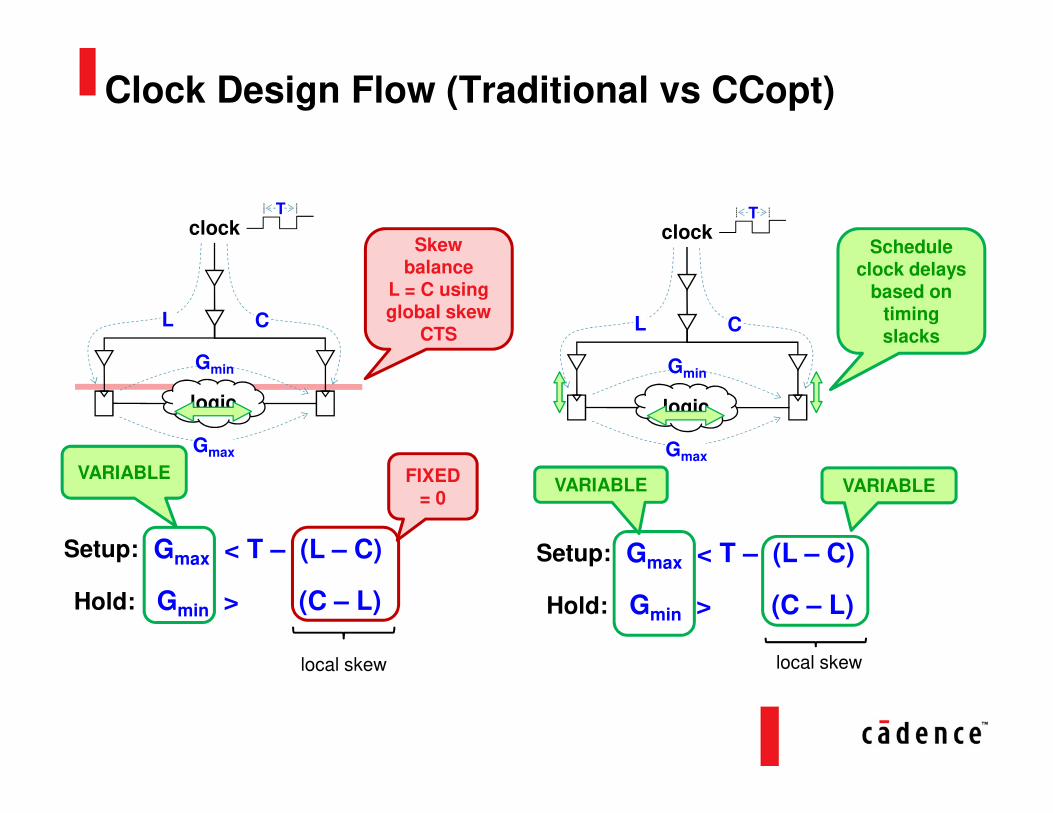
Clock Design Flow (Traditional vs CCopt)
Hold:
Setup:
clock
L C
Gmin
logic
Gmax
T
Gmin > (C – L)
Gmax < T – (L – C)
FIXED = 0
VARIABLE
Skew balance
L = C using global skew
CTS
local skew
Hold:
Setup:
clock
L C
Gmin
logic
Gmax
T
Gmin > (C – L)
Gmax < T – (L – C)
VARIABLEVARIABLE
Schedule clock delays
based on timing slacks
local skew

38 © 2017 Cadence Design Systems, Inc. Cadence confidential. Internal use only.
Advanced Low Power Techniques

39 © 2017 Cadence Design Systems, Inc. Cadence confidential. Internal use only.
Approaches for Greener IC
• EDA/Circuit Design Techniques
• Reduce Leakage (energy efficient)– Ideally, if leakage ~= 0, no need to do PSO
– No need for isolation (less area, less trouble)
• Reduce Vdd Voltage (low power)– V2 power reduction (>= 10x)
– Most appealing way! (as area, frequency going way up)

40 © 2017 Cadence Design Systems, Inc. Cadence confidential. Internal use only.
• Multi-Vt Swapping– HVT -> lower leakage
• Multi-Gate-Length Swapping– Longer gate-length -> lower leakage
• Stack-Forcing– Increate effective gate length for leakage reduction
• Poly-biasing– Increase gate-length at GDS level
Review: Traditional Leakage Power Optimization

April 5, 2017 Cadence Confidential: Cadence Internal Use Only41
Dynamic Voltage Frequency Scaling (DVFS)
• Description
– Varies the frequency and voltage of a design
– Done Real time
– Commonly used in processor design
– Based on system demand
• Power Savings
– Optimal voltage/Frequency level per
task per domain
– Improves both dynamic and leakage voltage
• Reduced frequency – produces less
switching power
• Reduced voltage means
– Less dynamic power
– Less leakage power
ModeControl
Voltage Island Voltage Island
A B
C
VoltageRegulators
Voltage Island
Pro
gra
mm
ab
le
Mode Domain A Domain B
High Perf. 1.2V800mhz
1.2V600mhz
Med Perf 1.0V600mhz
1.2V600mhz
Idle 0.8v400 mhz
0.8v400mhz

April 5, 2017 Cadence Confidential: Cadence Internal Use Only42
Required
Dynamic Voltage Frequency Scaling (DVFS)
Delivered
Disk r/w
Time
Text entryMPEG decode
Speed/Power
Required
Delivered
Disk r/w
Time
Text entryMPEG decode
Speed/Power
Without DVFS - deliver same power in all modes
3W average
DVFS provides a better match to requirements and can save
power over time
32
1
2W average power in this diagram, but varies based on
system requirements

April 5, 2017 Cadence Confidential: Cadence Internal Use Only43
Dual/Multi-Bit Flops- aka: Multi-Bit-Cell-Inference (MBCI)
• Inverters in flops tend to be oversized due to manufacturing ground rules.
• As we get into smaller geometries like 65nm and beyond the minimum size of clock driver can drive more than single flop.
• Combining registers into multi-bit instances reduces the total load on the clock tree.– Dual-bit or Quad-bit flops are designed
to efficiently distribute the internal clock signal to the master & slave elements of the flop.
• By using this we can reduce the leaf load on clock tree by a max 50%.
C
d
d
CC#
C C
C# C#
Masterlatch
Slavelatch
C C
C# C#
Masterlatch
Slavelatch
C
d
CC#
C C
C# C#
Masterlatch
Slavelatch

q
t
t
t
t
t
t
d
ttcp
Traditional register
q
t
t
t
d
ttcp
pulse clock
Pulsed latch
Pulse Generator
Dummy delayNegative edge FF memory
� Traditional FF is replaced with a pulsed-latch� Pulse generator is shared by several pulsed-latch� Dummy clock delay cell is used to balance clock tree
Pulsed Latch Design Methodology

April 5, 2017 Cadence Confidential: Cadence Internal Use Only45
Other Techniques to Reduce Clock Power
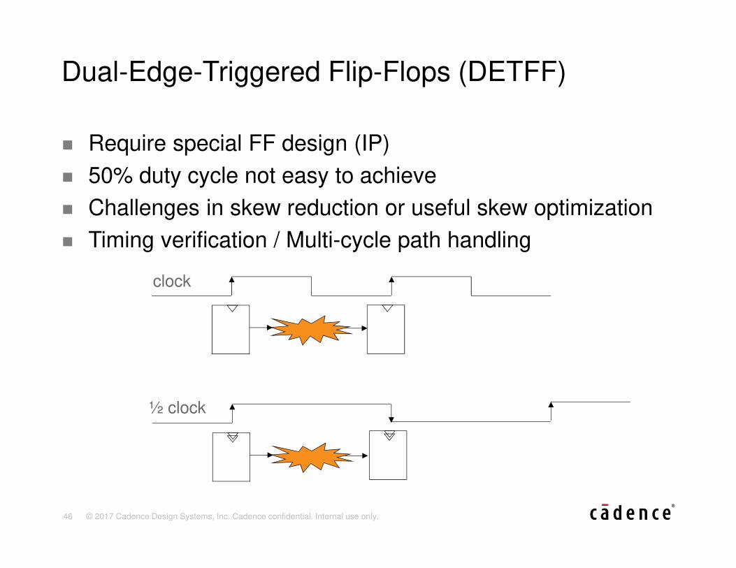
• Dual-Edge-Triggered FF (DET)
– Double data rate per cycle -> half the clock frequency
• Low Swing Clock (LSC)
– Use low voltages for clock tree
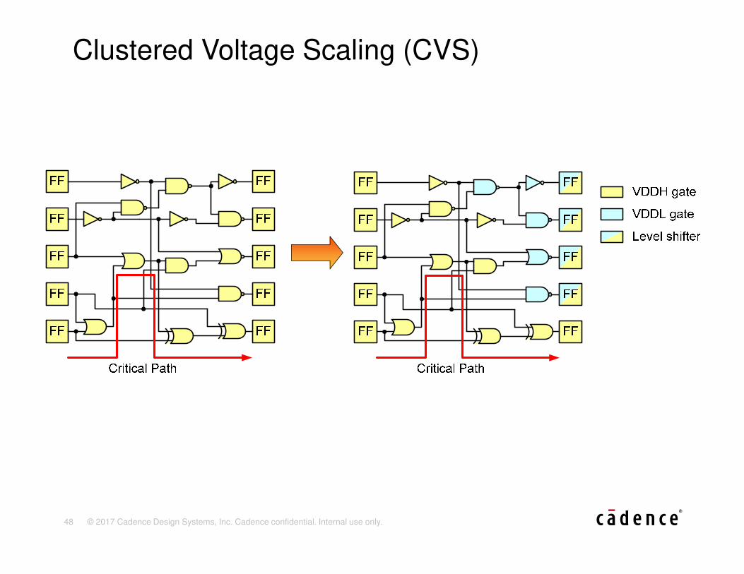
• Clustered Voltage Scaling (CVS)
– Extend LSC idea to data path w/ slacks
• Globally asynchronous locally synchronous (GALS)
– No more global clock
46 © 2017 Cadence Design Systems, Inc. Cadence confidential. Internal use only.
� Require special FF design (IP)
� 50% duty cycle not easy to achieve
� Challenges in skew reduction or useful skew optimization
� Timing verification / Multi-cycle path handling
Dual-Edge-Triggered Flip-Flops (DETFF)
clock
½ clock

47 © 2017 Cadence Design Systems, Inc. Cadence confidential. Internal use only.
Low Swing Clock Design
48 © 2017 Cadence Design Systems, Inc. Cadence confidential. Internal use only.
Clustered Voltage Scaling (CVS)
April 5, 2017 Cadence Confidential: Cadence Internal Use Only49
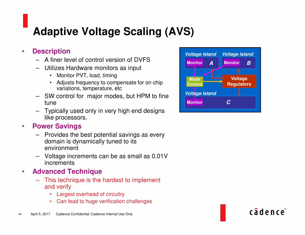
Adaptive Voltage Scaling (AVS)
• Description– A finer level of control version of DVFS
– Utilizes Hardware monitors as input• Monitor PVT, load, timing
• Adjusts frequency to compensate for on chip variations, temperature, etc
– SW control for major modes, but HPM to fine tune
– Typically used only in very high end designs like processors.
• Power Savings– Provides the best potential savings as every
domain is dynamically tuned to its environment
– Voltage increments can be as small as 0.01V increments
• Advanced Technique– This technique is the hardest to implement
and verify• Largest overhead of circuitry
• Can lead to huge verification challenges
ModeControl
Monitor Monitor
Monitor
Voltage Island Voltage Island
A B
C
VoltageRegulators
Voltage Island

50 © 2017 Cadence Design Systems, Inc. Cadence confidential. Internal use only.
Adaptive Back Bias Vt Control
PD-Default
PD3
PDM
+/-Vbb3PD2
PDM
+/-Vbb2
PD1
PDM
+/-Vbb1
• Concept applicable to AVS as well

51 © 2017 Cadence Design Systems, Inc. Cadence confidential. Internal use only.
• Turn off power to unused logic trees
• Operand isolation recognizes logic cones that are blocked– Extending this idea to Power Shut
Off, these unused logic cones could be powered off
module test (en,a,b,c,out);
input en;
input [7:0] a, b, c;
output [8:0] out;
assign out = en? a+b : a+c;
endmodule
+
+a
b
+out
en
c
en
+a
bout
c
PSO
PSO
Leakage Power Optimization:- Fine Grain PSO

52 © 2017 Cadence Design Systems, Inc. Cadence confidential. Internal use only.
PPA Optimization5%-20% leakage & dynamic
Relative ROI – Low Power Design Techniques
Low Impact High Impact
Low Saving
High Saving
Difficulty (Design Flow Impact)
Po
we
r S
av
ing
Clock Gating 15%-30% dynamic
Multi VT & Multi Length Gate~40% leakage
Advanced Clocking TechniquesAdvanced Clocking Techniques
Pulse Latch ~20% dynamic
DETFF~20% dynamic
Low-Swing Clocks~15% dynamic
Adv. OptimizationsAdv. Optimizations
MBCI5%-15% dynamic
CCOpt10%-20% dynamic & leakage
Advanced Low-Power Techniques
These apply to
power domains &
require power intent file
Advanced Low-Power Techniques
These apply to
power domains &
require power intent file
MSV~40% dynamic~20% leakage
Body Bias~40% leakage
PSO~95% leakage (in off-state)
Popularchoice
DVFS30%-50% dynamic15%-30% leakage
AVS30%-60% dynamic15%-45% leakage

53 © 2017 Cadence Design Systems, Inc. Cadence confidential. Internal use only.
Devices – Now & Future

54 © 2017 Cadence Design Systems, Inc. Cadence confidential. Internal use only.
Strained-Si, Hi-K/Metal Gate
• Reduce gate leakage (IG)– Thicker gate oxide (1.2nm->3.0nm)
– Harder for electron to tunnel directly through gate
– Need to compensate for speed lost– Strained Si to improve mobility at channel surface– Hi-K Dielectric Material (> 3.9)(15?) + Metal Gate
– Actual K value is a trade secret
– 5-100x reduction in IG

55 © 2017 Cadence Design Systems, Inc. Cadence confidential. Internal use only.
Review - Major Leakage Components for Small Geometry NMOS
Gate
Source Drain
0
Vdd
0
IG
Inversion
Gate
Source Drain
0
0
Vdd
Isubvt
IDIBLIGIDL
Ipn
* IG : direct tunneling + hot carrier injection
DIBL: drain-induced barrier loweringGIDL: gate-induced drain leakage

56 © 2017 Cadence Design Systems, Inc. Cadence confidential. Internal use only.
Well / Channel Engineering
Gate
Source Drain
Halo Doping
Super Steep Retrograde Doping
• Reduce channel (surface & under) leakage due to DIBL
• Improve Vt sensitivity to body bias– Allow adaptive Vt modulation by body bias (Isubvt)

April 5, 2017 Cadence Confidential: Cadence Internal Use Only57
SOI & FinFET

April 5, 2017 Cadence Confidential: Cadence Internal Use Only58
Why SOI
• Traditional bulk process limitations (28nm/14nm)– DVFS
• Voltage limited & performance degradation
– Poly biasing
• Limited range
– Dynamic transistor Vt control
• Limited body bias range (-300mV to +300mV)
• Limited benefit in 28nm, no benefit beyond 28nm
• SOI– No latch up
– No parasitic device
– Low soft-error due to alpha-particles
– No channel doping -> improve Vt variability (Vt can be much lower-> Vdd too!)
– Ultra-thin insulator -> large back-bias voltage possible (no GIDL)
– Ultra-thin body & buried-oxide (UTBB) -> better short-channel-effect
April 5, 2017 Cadence Confidential: Cadence Internal Use Only59
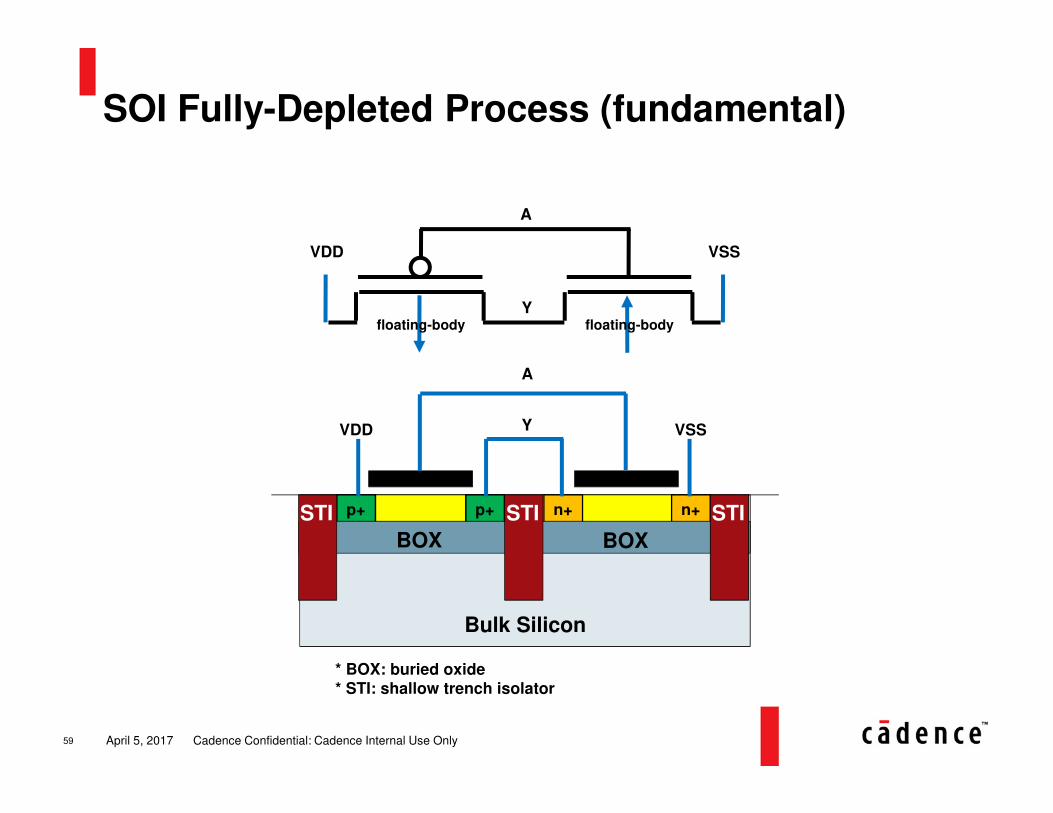
SOI Fully-Depleted Process (fundamental)
* BOX: buried oxide* STI: shallow trench isolator
Bulk Silicon
n+p+ n+p+
VDD VSS
A
Y
BOX
STI STISTI
BOX
A
Y
VDD VSS
floating-body floating-body

60 © 2017 Cadence Design Systems, Inc. Cadence confidential. Internal use only.
FinFET / Multi-gate FET
3-D View
Back Gate
Source Drain
Front Gate
Top Gate(optional)
Top View
Gate
Gate
Source Drain Thin Si (5-20nm)
Gate Ox
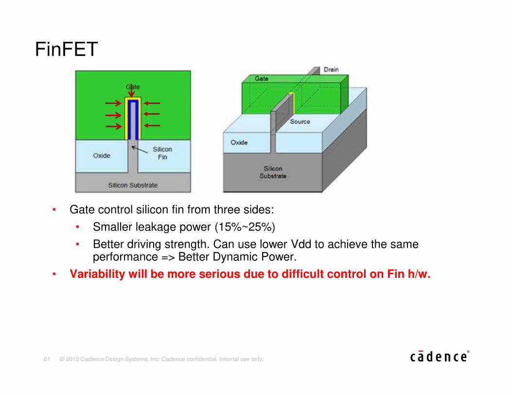
61 © 2012 Cadence Design Systems, Inc. Cadence confidential. Internal use only.
FinFET
• Gate control silicon fin from three sides:
• Smaller leakage power (15%~25%)
• Better driving strength. Can use lower Vdd to achieve the same performance => Better Dynamic Power.
• Variability will be more serious due to difficult control on Fin h/w.

SOI vs FinFET – Comparison Chart (Biased)
April 5, 2017 Cadence Confidential: Cadence Internal Use Only62
Source: SoC Differentiation using FDSOI – a Manufacturing Partner’s Perspective, Shigeru Shimauchi, GlobalFoundry(FD-SOI Workshop, June 15, 2013, Kyoto)
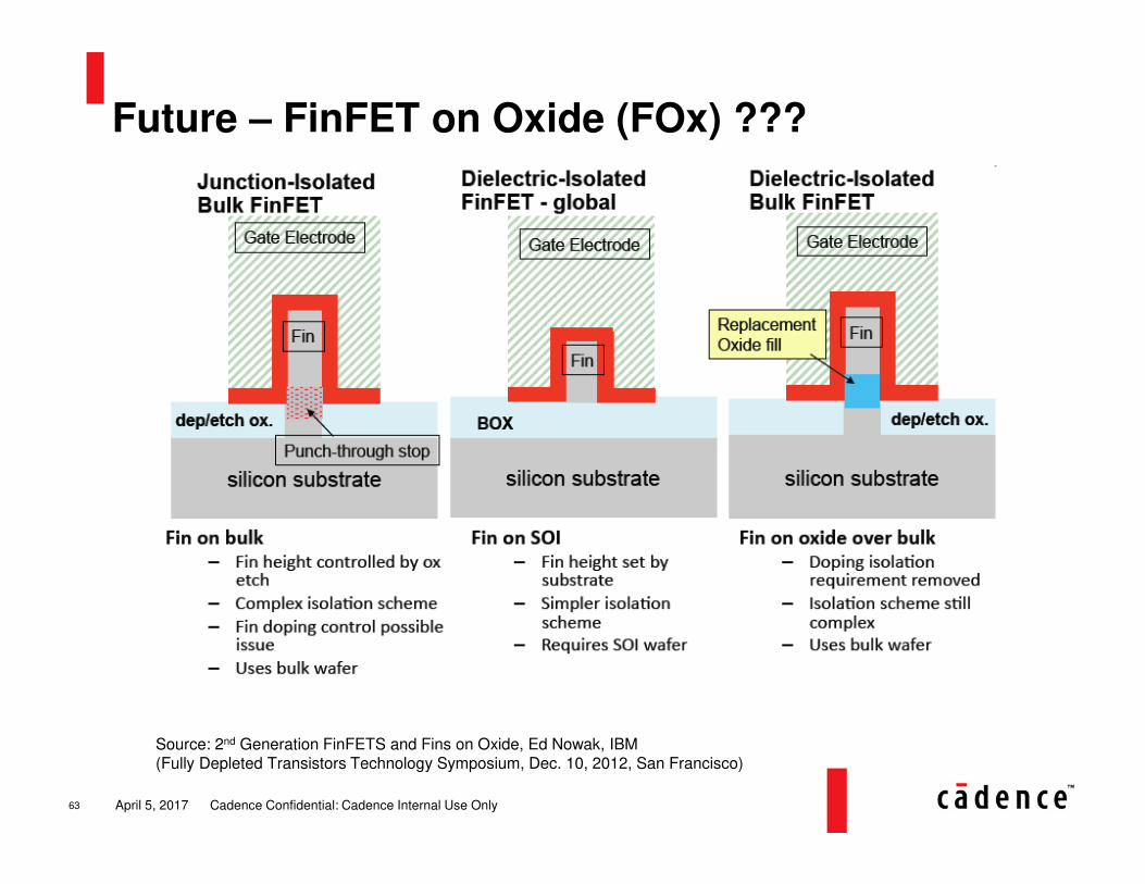
Future – FinFET on Oxide (FOx) ???
April 5, 2017 Cadence Confidential: Cadence Internal Use Only63
Source: 2nd Generation FinFETS and Fins on Oxide, Ed Nowak, IBM(Fully Depleted Transistors Technology Symposium, Dec. 10, 2012, San Francisco)

April 5, 2017 Cadence Confidential: Cadence Internal Use Only64
Advanced Devices

ITRS 2.0 Logic Voltage Road Map (2015)
April 5, 2017 Cadence Confidential: Cadence Internal Use Only65
Source: International Technology Roadmap for Semiconductors 2.0 Executive Report 2015, pp 34
ITRS-2.0 2015 2017 2019 2021 2024 2027 2030
Node(GL) 16/14(28) 11/10(22) 8/7(18) 6/5(14) 4/3(11) 3/2.5(9) 2/1.5(7)
VDD 0.80 0.75 0.70 0.65 0.55 0.45 0.40
DeviceFinFET
FDSOI
FinFet
FDSOI
FinFET
LGAA
FinFET
LGAA
VGAA
VGAA
M3D
VGAA
M3D
VGAA
M3D
LGAA: lateral gate-all-around; VGAA: vertical gate-all-around; M3D: monolithic 3D IC
• Voltage does NOT scaled linearly w.r.t. node(gate-length)
• Bottleneck: variation & reliability
– Random dopant fluctuation (RDF)
– Static noise margin (SNM)
• Minimum voltage requirement (Vmin)

• Equivalent Scaling (traditional – maintain constant E-field)
– Strained Si (90nm)
– High-K Metal Gate (HK/MG – 45nm)
– FinFET (22nm)
– Non-Si: Germaniun
• 3D Power Scaling (future <=10nm)
– Monolithic 3D (running out of horizontal space)
– Combination of 3-D architecture (FinFET) & low power device
– Gate-all-around (GAA): Lateral (LGAA), Vertical (VGAA)
For 10nm and Below
April 5, 2017 Cadence Confidential: Cadence Internal Use Only66
Source: International Technology Roadmap for Semiconductors 2.0 Executive Report 2015, pps 2,32-38

Device Natural Length
• Natural length– The lateral distance of E field that drain can influence (Vt) under the gate
channel area
– The longer the worse!
– Traditionally (bulk Si) gate length was chosen to be 4x to 6x of natural length
• Gate-all-around (GAA) to increase n to reduce natural length
April 5, 2017 Cadence Confidential: Cadence Internal Use Only67
�� =1
�
��
����
Hi-KGate-oxide ~= 1.2nm (~= 5 Si atoms)
n = number of gates of device

Natural Lengths for Various Devices
April 5, 2017 Cadence Confidential: Cadence Internal Use Only68
2D Bulk/SOI
n=1
3D FinFET
n=2..3
LGAA (horizontal)
n=3
VGAA (vertical)
n>=4
• Practical gate-length limit– FinFET: 8nm
– GAA: 3nm has been demonstrated (Ansari et al, Applied Physics Letter, 2010)

New Materials, New Physics & Quantum Effect
• Ultra-low-power applications
– Operating voltage below Vt
• Ie, leakage current (today) = operating current (future)
• subthreshold slope 60mV/dec thermal voltage limitation
– New (non-Si) Materials & Non-MOS-like devices
• Eg, no PN-junction
– Quantum effect governs at extreme small dimension (smaller than FinFET)
• Eg. Tunneling
• Examples and active research topics:
– Nanowire transistor (NWT)
– Carbon-nanotube transistor (CNT)
– Junction-less transistor (JNT)
– III-V compounds: GaSb-InAs, GaAs, …
– Combination of group IV: graphene, Ge-Sn, …
– Tunneling FET (TFET)
– Metal-Semimetal-Metal (all same material w/o PN junction, eg Sn)
– Band-gap engineering (extreme small dimemsion widens the metal band-gap!)
(All of the above are formulated w/ Poisson and Schroedinger eq. and can be solved w/ perturbation approach)
April 5, 2017 Cadence Confidential: Cadence Internal Use Only69

70 © 2017 Cadence Design Systems, Inc. Cadence confidential. Internal use only.
Research Example: Low Voltage (Green)FET
* “Green Transistor - A VDD Scaling Path for Future Low Power ICs,” C. Hu et al, VLSI-TSA 2008
Gate
N+ Source P+ Drain
P+ Pocket(controlled dopingat verge of breakdown)
h+
Small Vgs (<0) to causeZener breakdown (BTBT)to generate e-/h+ current
e-
• Based on Band-To-Band Tunneling (BTBT)– Identical to GIDL mechanism (leakage -> useful current)
– Rely on carrier going through (instead of over) barrier
– Operate at Vdd ~= 0.2V (10x power reduction)
– Experimental, no Si yet
Research Institutes for Ultra-Low-Power Devices
• STARnet
– Semiconductors Technology Advanced Research network
• NRI
– Nanotechnology Research Initiative
• LEAST
– Center for Low Energy Systems Technology
April 5, 2017 Cadence Confidential: Cadence Internal Use Only71

72 © 2017 Cadence Design Systems, Inc. Cadence confidential. Internal use only.
Summary

73 © 2017 Cadence Design Systems, Inc. Cadence confidential. Internal use only.
Low power is the future, and the future is now!
• Minimize P ! (eg. if V is fixed, minimize C*f, not C or f alone)
• Think high level - the higher the level, the better the ROI
• Power(energy) must be part of cost consideration at all levels of design
• Beware of what future technologies can bring, and be prepared for them– Due to technology advancement, some techniques may not have good ROI
– Eg. with FinFET, leakage optimization might not be necessary
– Scaling: beware of Reliability, Variability, & Static Noise Margin (SNM)

74 © 2017 Cadence Design Systems, Inc. Cadence confidential. Internal use only.
Q & A


76 © 2017 Cadence Design Systems, Inc. Cadence confidential. Internal use only.
Appendix

April 5, 2017 Cadence Confidential: Cadence Internal Use Only77
Low Power Techniques at Other Levels

78 © 2017 Cadence Design Systems, Inc. Cadence confidential. Internal use only.
Register-Transfer Level
• State assignment / encoding, use of DC
• Multi-level power-aware logic transformation/optimization
• Pre-computation (Shannon’s expansion)
• Operand isolation / data gating
• Global bus splitting & partitioning / Dedicated bus– Bus-splitter / router (NoC)
• Power-off unused units
• Factoring
• Operation substitution / reduction (while maintaining throughput)
• Technology mapping (choice of cell)
• Choice of components– Eg. Ripple-carry instead of CLA: slower but lower power
• Pipelining (scale the voltage on the pipelined blocks)– Same throughput, less power
• Parallel Processing (scale the voltage on the parallel blocks)
• Memory reorganization (split up memory lookup)
• Datapath Reordering (glitch avoidance)

79 © 2017 Cadence Design Systems, Inc. Cadence confidential. Internal use only.
Architectural Level
• Asynchronous design, GALS
• Multiple power modes (degree of “darkness”)– Active, alive, drowsy, nap, doze, sleep, (light/deep/deeper) sleep, off, dark, dim, …
• On-Offfff-On-Offfff-On operation instead of AO (requires profiling)
• Approximate Computation (imperfect, inaccurate,…)– Qos select controlled by HW/SW/user
• Redundant/Parallel computation units – HP & LP version
• Domain-specific accelerators
• Minimize memory access
• Minimize number of operations (*, +)
• High-level resource allocation & scheduling– Minimize data movement
• Proper representation of data– Use sign-mag instead of 2’s comp if appropriate (eg, when sign changes frequently)
– Gray coding (if data bits changes sequentially – eg. instruction memory address)

80 © 2017 Cadence Design Systems, Inc. Cadence confidential. Internal use only.
System/App/Software Level (some examples)
• Rework software to minimize power– Choice of Algorithm
– If can do in O(n log n), don’t do in O(n^2)
– Eg. Proper vector quantization (VQ) algorithm – differential tree search instead of full
– Remove redundant activities in code– Eg. refresh rate 60Hz of the same screen
– Eg. frame update = 60 FPS of the same frame
– 30%-40% power saving (DAC 2014), similar image quality
– Generate low power version of the original image– Partial display disable/dim
– Color remap
– Substantial power saving (configuration dependent) (DAC 2014)
• Activity monitoring & activity-based SW DVFS control– Eg. either CPU is bottleneck or GPU is, but not both
– DVFS on CPU or GPU depending on the current activity
– 30% power saving on average (DAC 2014)
• Dark Silicon– Dynamically configure/program the NoC “ON-OFF” routers & blocks by software
– Substantial power saving (DAC 2014) (algorithm dependent)

81 © 2017 Cadence Design Systems, Inc. Cadence confidential. Internal use only.
Circuit / Cell / Memory / IP Level
• Multi-Stacking / Multi-Gate-Length / Multi-Vt
• Multi-supply / Multi-rail
• Back-bias support (FBB / RBB)
• Minimize internal node glitches
• Minimize internal node cap
• Fast internal node slew rate
• Use static circuit & minimize dynamic circuit & pre-charging– Eg. Schmitt-trigger inverter based gates (ISSCC 2011)
• Combine logic & latch in single cell (eg. Alpha latch)
• Memory / IP– Built-in multiple power modes with power management unit
– Smaller banks, decoder logic
– Shorter bit-line, Word-line under-drive (unselected cells remain at low voltage)
– Internal DVFS
– Result caching (prevent redundant lookup – the core can stay at low voltage)
• Analog Components– PLL/DLL partitioning (phase detector sharing among partitions)
• Post-Si Calibration/trimming, Poly-biasing