low-power dual channel digital isolators (rev. f) · outx gndi gndo inx v cci v cco isolation...
TRANSCRIPT

OUTx
GNDOGNDI
INx
VCCOVCCI
Isolation Capacitor
Product
Folder
Sample &Buy
Technical
Documents
Tools &
Software
Support &Community
ISO7420E, ISO7420FE, ISO7421E, ISO7421FESLLSE45F –DECEMBER 2010–REVISED JULY 2015
ISO742x Low-Power Dual Channel Digital Isolators1 Features 3 Description
ISO742x provide galvanic isolation up to 2500 VRMS1• Signaling Rate > 50 Mbpsfor 1 minute per UL and 4242 VPK per VDE. These• Default Output 'High' and 'Low' Options devices have two isolated channels. Each channel
• Low Power Consumption: Typical ICC per Channel has a logic input and output buffer separated by a(3.3-V Supplies): silicon dioxide (SiO2) insulation barrier. Used in
conjunction with isolated power supplies, these– ISO7420: 1.4 mA at 1 Mbps, 2.5 mA atdevices prevent noise currents on a data bus or other25 Mbpscircuit from entering the local ground and interfering
– ISO7421: 1.8 mA at 1 Mbps, 2.8 mA at with or damaging sensitive circuitry. ISO7420 has25 Mbps both channels in the same direction while ISO7421
has the two channels in opposite direction. In case of• Low Propagation Delay: 7 ns Typicalinput power or signal loss, default output is 'low' for• Low Pulse Skew: 200 ps Typicaldevices with suffix 'F' and 'high' for devices without
• Wide TA Range Specified: –40°C to 125°C suffix 'F'. ISO742x have no integrated noise filter and• 50-KV/μs Transient Immunity, Typical thus have fast propagation delays.• Isolation Barrier Life: > 25 Years These devices have TTL input thresholds and• Operates from 3-V to 5.5-V Supply Levels operate from 3-V to 5.5-V supplies. All inputs are 5-V
tolerant when supplied from a 3.3-V supply.• 3.3-V and 5-V Level Translation• Narrow Body SOIC-8 Package Device Information(1)
• Safety and Regulatory Approvals: PART NUMBER PACKAGE BODY SIZE (NOM)– 4242 VPK Isolation per DIN V VDE V 0884-10 ISO7420E
and DIN EN 61010-1 ISO7420FESOIC (8) 4.90 mm x 3.91 mm– 2500 VRMS Isolation for 1 minute per UL 1577 ISO7421E
– CSA Component Acceptance Notice 5A, IEC ISO7421FE60950-1 and IEC 61010-1 Standards (1) For all available packages, see the orderable addendum at
the end of the datasheet.– CQC Certification per GB4943.1-2011–
Simplified Schematic2 Applications• Opto-Coupler Replacement in:
– Industrial FieldBus– ProfiBus– ModBus– DeviceNet™ Data Buses
– Servo Control Interface– Motor Control VCCI and GNDI are supply and ground
connections respectively for the input– Power Supplieschannels.
– Battery PacksVCCO and GNDO are supply and groundconnections respectively for the outputchannels.
1
An IMPORTANT NOTICE at the end of this data sheet addresses availability, warranty, changes, use in safety-critical applications,intellectual property matters and other important disclaimers. PRODUCTION DATA.

ISO7420E, ISO7420FE, ISO7421E, ISO7421FESLLSE45F –DECEMBER 2010–REVISED JULY 2015 www.ti.com
Table of Contents10%.......................................................................... 111 Features .................................................................. 1
6.14 Typical Characteristics .......................................... 122 Applications ........................................................... 17 Parameter Measurement Information ................ 153 Description ............................................................. 18 Detailed Description ............................................ 164 Revision History..................................................... 2
8.1 Overview ................................................................. 165 Pin Configuration and Functions ......................... 48.2 Functional Block Diagram ....................................... 166 Specifications......................................................... 58.3 Feature Description................................................. 176.1 Absolute Maximum Ratings ..................................... 58.4 Device Functional Modes........................................ 206.2 ESD Ratings.............................................................. 5
9 Applications and Implementation ...................... 216.3 Recommended Operating Conditions....................... 59.1 Application Information............................................ 216.4 Thermal Information .................................................. 59.2 Typical Application ................................................. 216.5 Electrical Characteristics: VCC1 and VCC2 = 5 V ±
10%............................................................................ 6 10 Power Supply Recommendations ..................... 246.6 Electrical Characteristics: VCC1 = 5 V ± 10%, VCC2 = 11 Layout................................................................... 25
3.3 V ± 10% ............................................................... 7 11.1 Layout Guidelines ................................................. 256.7 Electrical Characteristics: VCC1 = 3.3 V ± 10%, VCC2 11.2 Layout Example .................................................... 25
= 5 V ± 10% ............................................................... 812 Device and Documentation Support ................. 266.8 Electrical Characteristics: VCC1 and VCC2 = 3.3 V ±
12.1 Documentation Support ........................................ 2610%............................................................................ 912.2 Related Links ........................................................ 266.9 Power Dissipation Characteristics ............................ 912.3 Community Resources.......................................... 266.10 Switching Characteristics: VCC1 and VCC2 = 5 V ±12.4 Trademarks ........................................................... 2610%.......................................................................... 1012.5 Electrostatic Discharge Caution............................ 266.11 Switching Characteristics: VCC1 = 5 V ± 10%, VCC2
= 3.3 V ± 10% .......................................................... 10 12.6 Glossary ................................................................ 266.12 Switching Characteristics: VCC1 = 3.3 V ± 10%, 13 Mechanical, Packaging, and Orderable
VCC2 = 5 V ± 10% .................................................... 11 Information ........................................................... 266.13 Switching Characteristics: VCC1 and VCC2 = 3.3 V ±
4 Revision HistoryNOTE: Page numbers for previous revisions may differ from page numbers in the current version.
Changes from Revision E (January 2013) to Revision F Page
• Changed the datasheet format to the new TI standard.......................................................................................................... 1• Added Pin Configuration and Functions section, ESD Ratings table, Feature Description section, Device Functional
Modes, Application and Implementation section, Power Supply Recommendations section, Layout section, Deviceand Documentation Support section, and Mechanical, Packaging, and Orderable Information section .............................. 1
• Deleted text from the Description: "CC-grade devices have integrated 10ns-filters for harsh environments whereshort noise pulses may be present at the device input pins." ................................................................................................ 1
• VDE standard changed to DIN V VDE V 0884-10 (VDE V 0884-10):2006-12 ...................................................................... 1• Deleted CC-grade from tPLH, tPHL in the Switching Characteristics table.............................................................................. 10• Deleted CC-grade from tPLH, tPHL in the Switching Characteristics table.............................................................................. 10• Deleted CC-grade from tPLH, tPHL in the Switching Characteristics table.............................................................................. 11• Deleted CC-grade from tPLH, tPHL in the Switching Characteristics table.............................................................................. 11• Changed the Available Options Table To the Feature Description table ............................................................................. 17
Changes from Revision D (December 2011) to Revision E Page
• Deleted devices ISO7420FCC and ISO7421FCC.................................................................................................................. 1• Changed the NOTE: text ...................................................................................................................................................... 17• Added table Note to VIORM .................................................................................................................................................... 18• Changed Z to Undetermined for the OUTPUT OUTA, OUTB column of the FUNCTION TABLE....................................... 20
2 Submit Documentation Feedback Copyright © 2010–2015, Texas Instruments Incorporated
Product Folder Links: ISO7420E ISO7420FE ISO7421E ISO7421FE

ISO7420E, ISO7420FE, ISO7421E, ISO7421FEwww.ti.com SLLSE45F –DECEMBER 2010–REVISED JULY 2015
Changes from Revision C (March 2011) to Revision D Page
• Changed SAFETY feature Bullet From: UL 1577 Approved; Other Approvals Pending To: All Agencies ApprovalsCompleted .............................................................................................................................................................................. 1
• Changed the REGULATORY INFORMATION table ............................................................................................................ 18
Changes from Revision B (January 2011) to Revision C Page
• Added devices ISO7420FCC and ISO7421FCC.................................................................................................................... 1• Changed Feature bullet To: Low Propagation Delay: 7 ns Typical (E-Grade)....................................................................... 1• Changed Feature bullet To: Low Pulse Skew: 200 Typical (E-Grade)................................................................................... 1• Changed the SAFETY and REGULATORY APPROVALS list............................................................................................... 1• Changed the data sheet DESCRIPTION................................................................................................................................ 1• Changed the Supply Current values for ISO7421x at 10, 25, and 50 Mbps.......................................................................... 6• Changed the Supply Current values for ISO7421x at 10, 25, and 50 Mbps.......................................................................... 7• Changed the Supply Current values for ISO7421x at 10, 25, and 50 Mbps.......................................................................... 8• Changed the Supply Current values for ISO7421x 25 and 50 Mbps ..................................................................................... 9• Added CC-grade and valued to tPLH, tPHL in the Switching Characteristics table ................................................................. 10• Added ISO7421x values for Pulse width distortion, Channel-to-channel output skew time, and Part-to-part skew time .... 10• Added CC-grade and valued to tPLH, tPHL in the Switching Characteristics table ................................................................. 10• Added ISO7421x values for Pulse width distortion and Channel-to-channel output skew time........................................... 10• Added CC-grade and valued to tPLH, tPHL in the Switching Characteristics table ................................................................. 11• Added CC-grade and valued to tPLH, tPHL in the Switching Characteristics table ................................................................. 11• Added graphs Figure 5, Figure 6, Figure 7, and Figure 8.................................................................................................... 12• Added graphs Figure 14 and Figure 15................................................................................................................................ 13• Changed Note 1 Figure 16 ................................................................................................................................................... 15• Changed Figure 17............................................................................................................................................................... 15• Changed the Available Options Table.................................................................................................................................. 17• Changed Isolation resistance test conditions ....................................................................................................................... 17• Changed the values of VIORM and VPR in the INSULATION CHARACTERISTICS table ..................................................... 18• Changed the value of VIOTM in the INSULATION CHARACTERISTICS table From: 4000 To: 4242 .................................. 18• Changed Figure 21............................................................................................................................................................... 19• Changed PU to X in the last row of the FUNCTION TABLE................................................................................................ 20• Added section: SUPPLY CURRENT EQUATIONS.............................................................................................................. 22
Changes from Revision A (December 2010) to Revision B Page
• Changed Feature bullet From: ISO7421: TBDmA at 1Mbps, TBDmA at 25Mbps To: ISO7421: 1.8mA at 1Mbps,2.8mA at 25Mbps ................................................................................................................................................................... 1
• Updated the ISO7421x Supply Current values for VCC1 and VCC2 = 5V................................................................................. 6• Updated the ISO7421x Supply Current values for VCC1 = 5V and VCC2 = 3.3V ..................................................................... 7• Updated the ISO7421x Supply Current values for VCC1 = 3.3V and VCC2 = 5V ..................................................................... 8• Updated the ISO7421x Supply Current values for VCC1 and VCC2 = 3.3V.............................................................................. 9
Changes from Original (December 2010) to Revision A Page
• Changed the Max values for Supply current for VCC1 and VCC2, CL = 15pF........................................................................... 9
Copyright © 2010–2015, Texas Instruments Incorporated Submit Documentation Feedback 3
Product Folder Links: ISO7420E ISO7420FE ISO7421E ISO7421FE

VCC1
OUTA
INB
GND1
VCC2
INA
OUTB
GND2
1
2
3
4
8
7
6
5
Iso
latio
n
VCC1
INA
INB
GND1
VCC2
OUTA
OUTB
GND2
1
2
3
4
8
7
6
5
Iso
latio
n
ISO7420E, ISO7420FE, ISO7421E, ISO7421FESLLSE45F –DECEMBER 2010–REVISED JULY 2015 www.ti.com
5 Pin Configuration and Functions
ISO7420 D PackageISO7421 D Package8-Pin SOIC
8-Pin SOICTop ViewTop View
Pin FunctionsPIN
I/O DESCRIPTIONNAME ISO7420x ISO7421xINA 2 7 I Input, channel AINB 3 3 I Input, channel BGND1 4 4 – Ground connection for VCC1
GND2 5 5 – Ground connection for VCC2
OUTA 7 2 O Output, channel AOUTB 6 6 O Output, channel BVCC1 1 1 – Power supply, VCC1
VCC2 8 8 – Power supply, VCC2
4 Submit Documentation Feedback Copyright © 2010–2015, Texas Instruments Incorporated
Product Folder Links: ISO7420E ISO7420FE ISO7421E ISO7421FE

ISO7420E, ISO7420FE, ISO7421E, ISO7421FEwww.ti.com SLLSE45F –DECEMBER 2010–REVISED JULY 2015
6 Specifications
6.1 Absolute Maximum Ratings (1)
MIN MAX UNITVCC Supply voltage (2), VCC1, VCC2 –0.5 6 VVI Voltage at IN, OUT –0.5 VCC + 0.5 (3) VIO Output current ±15 mAVSRG Maximum surge immunity - Supports IEC 61000-4-5 4000 VPK
TJ(Max) Maximum junction temperature 150 °CTstg Storage temperature –65 150 °C
(1) Stresses beyond those listed under Absolute Maximum Ratings may cause permanent damage to the device. These are stress ratingsonly and functional operation of the device at these or any other conditions beyond those indicated under recommended operatingconditions is not implied. Exposure to absolute-maximum-rated conditions for extended periods may affect device reliability.
(2) All voltage values are with respect to network ground terminal and are peak voltage values.(3) Maximum voltage must not exceed 6 V.
6.2 ESD RatingsVALUE UNIT
Human body model (HBM), per ANSI/ESDA/JEDEC JS-001 (1) ±3000V(ESD) Electrostatic discharge Charged-device model (CDM), per JEDEC specification JESD22-C101 (2) ±1500 V
Machine model (MM) ANSI/ESDS5.2-1996 ±200
(1) JEDEC document JEP155 states that 500-V HBM allows safe manufacturing with a standard ESD control process.(2) JEDEC document JEP157 states that 250-V CDM allows safe manufacturing with a standard ESD control process.
6.3 Recommended Operating ConditionsMIN NOM MAX UNIT
VCC1, VCC2 Supply voltage 3.0 5.5 VIOH High-level output current –4 mAIOL Low-level output current 4 mAVIH High-level input voltage 2 5.5 VVIL Low-level input voltage 0 0.8 Vtui Input pulse duration 20 ns1 / tui Signaling rate 0 50 (1) MbpsTJ
(2) Junction temperature –40 136 °CTA Ambient Temperature -40 25 125 °C
(1) Under typical conditions, these devices are capable of signaling rate > 150 Mbps.(2) To maintain the recommended operating conditions for TJ, see the Thermal Information table.
6.4 Thermal InformationISO742x
THERMAL METRIC (1) D (SOIC) UNIT8 PINS
RθJA Low-K board 212Junction-to-ambient thermal °C/Wresistance High-K board 116.6RθJC(top) Junction-to-case (top) thermal resistance 71.6 °C/WRθJB Junction-to-board thermal resistance 57.3 °C/WψJT Junction-to-top characterization parameter 28.3 °C/WψJB Junction-to-board characterization parameter 56.8 °C/W
(1) For more information about traditional and new thermal metrics, see the Semiconductor and IC Package Thermal Metrics applicationreport, SPRA953.
Copyright © 2010–2015, Texas Instruments Incorporated Submit Documentation Feedback 5
Product Folder Links: ISO7420E ISO7420FE ISO7421E ISO7421FE

ISO7420E, ISO7420FE, ISO7421E, ISO7421FESLLSE45F –DECEMBER 2010–REVISED JULY 2015 www.ti.com
6.5 Electrical Characteristics: VCC1 and VCC2 = 5 V ± 10%TA = –40°C to 125°C
PARAMETER TEST CONDITIONS MIN TYP MAX UNIT
IOH = –4 mA; see Figure 16. VCCO(1)– 0.8 4.6
VOH High-level output voltage VIOH = –20 μA; see Figure 16. VCCO– 0.1 5
IOL = 4 mA; see Figure 16. 0.2 0.4VOL Low-level output voltage V
IOL = 20 μA; see Figure 16. 0 0.1
VI(HYS) Input threshold voltage hysteresis 400 mV
IIH High-level input current 10 μAINx at 0 V or VCCI
(1)
IIL Low-level input current –10 μA
CMTI Common-mode transient immunity VI = VCCI or 0 V; see Figure 18. 25 50 kV/μs
SUPPLY CURRENT (ALL INPUTS SWITCHING WITH SQUARE WAVE CLOCK SIGNAL FOR DYNAMIC ICC MEASUREMENT)
ISO7420x
ICC1 0.4 0.8DC Input: VI = VCCI or 0 V,DC to 1 Mbps AC Input: CL = 15 pFICC2 3.4 5
ICC1 0.6 110 Mbps
ICC2 4.5 6Supply current for VCC1 and VCC2 mA
ICC1 1 1.525 Mbps CL = 15 pF
ICC2 6.2 8
ICC1 1.7 2.550 Mbps
ICC2 9 12
ISO7421x
ICC1 2.3 3.6DC Input: VI = VCCI or 0 V,DC to 1 Mbps AC Input: CL = 15 pFICC2 2.3 3.6
ICC1 2.9 4.510 Mbps
ICC2 2.9 4.5Supply current for VCC1 and VCC2 mA
ICC1 4.3 625 Mbps CL = 15 pF
ICC2 4.3 6
ICC1 6 8.550 Mbps
ICC2 6 8.5
(1) VCCI = Input-side VCC; VCCO = Output-side VCC
6 Submit Documentation Feedback Copyright © 2010–2015, Texas Instruments Incorporated
Product Folder Links: ISO7420E ISO7420FE ISO7421E ISO7421FE

ISO7420E, ISO7420FE, ISO7421E, ISO7421FEwww.ti.com SLLSE45F –DECEMBER 2010–REVISED JULY 2015
6.6 Electrical Characteristics: VCC1 = 5 V ± 10%, VCC2 = 3.3 V ± 10%TA = –40°C to 125°C
PARAMETER TEST CONDITIONS MIN TYP MAX UNIT
IOH = –4 mA; ISO7421x (5-V side) VCC1 – 0.8 4.6see Figure 16. ISO7420x/7421x (3.3-V side) VCC2 - 0.4 3
VOH High-level output voltage VIOH = –20 μA; ISO7421x (5-V side) VCC1 – 0.1 5see Figure 16, ISO7420x/7421x (3.3-V side) VCC2 – 0.1 3.3
IOL = 4 mA; see Figure 16. 0.2 0.4VOL Low-level output voltage V
IOL = 20 μA; see Figure 16. 0 0.1
VI(HYS) Input threshold voltage hysteresis 400 mV
IIH High-level input current 10 μAINx at 0 V or VCCI
IIL Low-level input current –10 μA
CMTI Common-mode transient immunity VI = VCCI or 0 V; see Figure 18. 25 50 kV/μs
SUPPLY CURRENT (ALL INPUTS SWITCHING WITH SQUARE WAVE CLOCK SIGNAL FOR DYNAMIC ICC MEASUREMENT)
ISO7420x
ICC1 0.4 0.8DC Input: VI = VCCI or 0 V,DC to 1 Mbps AC Input: CL = 15 pFICC2 2.6 3.7
ICC1 0.6 110 Mbps
ICC2 3.3 4.3Supply current for VCC1 and VCC2 mA
ICC1 1 1.525 Mbps CL = 15 pF
ICC2 4.4 5.6
ICC1 1.7 2.550 Mbps
ICC2 6.2 7.5
ISO7421x
ICC1 2.3 3.6DC Input: VI = VCCI or 0 V,DC to 1 Mbps AC Input: CL = 15 pFICC2 1.8 2.8
ICC1 2.9 4.510 Mbps
ICC2 2.2 3.2Supply current for VCC1 and VCC2 mA
ICC1 4.3 625 Mbps CL = 15 pF
ICC2 2.8 4.1
ICC1 6 8.550 Mbps
ICC2 3.8 5.5
Copyright © 2010–2015, Texas Instruments Incorporated Submit Documentation Feedback 7
Product Folder Links: ISO7420E ISO7420FE ISO7421E ISO7421FE

ISO7420E, ISO7420FE, ISO7421E, ISO7421FESLLSE45F –DECEMBER 2010–REVISED JULY 2015 www.ti.com
6.7 Electrical Characteristics: VCC1 = 3.3 V ± 10%, VCC2 = 5 V ± 10%TA = –40°C to 125°C
PARAMETER TEST CONDITIONS MIN TYP MAX UNIT
ISO7421x (3.3-V side) VCC1 – 0.4 3IOH = –4 mA; seeFigure 16. ISO7420x/7421x (5-V side) VCC2 – 0.8 4.6
VOH High-level output voltage VISO7421x (3.3-V side) VCC1 – 0.1 3.3IOH = –20 μA;
see Figure 16 ISO7420x/7421x (5-V side) VCC2 – 0.1 5
IOL = 4 mA; see Figure 16. 0.2 0.4VOL Low-level output voltage V
IOL = 20 μA; see Figure 16. 0 0.1
VI(HYS) Input threshold voltage hysteresis 400 mV
IIH High-level input current 10 μAINx at 0 V or VCCI
IIL Low-level input current –10 μA
CMTI Common-mode transient immunity VI = VCCI or 0 V; see Figure 18. 25 50 kV/μs
SUPPLY CURRENT (ALL INPUTS SWITCHING WITH SQUARE WAVE CLOCK SIGNAL FOR DYNAMIC ICC MEASUREMENT)
ISO7420x
ICC1 0.2 0.4DC Input: VI = VCCI or 0 V,DC to 1 Mbps AC Input: CL = 15 pFICC2 3.4 5
ICC1 0.4 0.610 Mbps
ICC2 4.5 6Supply current for VCC1 and VCC2 mA
ICC1 0.6 0.925 Mbps CL = 15 pF
ICC2 6.2 8
ICC1 1 1.350 Mbps
ICC2 9 12
ISO7421x
ICC1 1.8 2.8DC Input: VI = VCCI or 0 V,DC to 1 Mbps AC Input: CL = 15 pFICC2 2.3 3.6
ICC1 2.2 3.210 Mbps
ICC2 2.9 4.5Supply current for VCC2 and VCC2 mA
ICC1 2.8 4.125 Mbps CL = 15 pF
ICC2 4.3 6
ICC1 3.8 5.550 Mbps
ICC2 6 8.5
8 Submit Documentation Feedback Copyright © 2010–2015, Texas Instruments Incorporated
Product Folder Links: ISO7420E ISO7420FE ISO7421E ISO7421FE

ISO7420E, ISO7420FE, ISO7421E, ISO7421FEwww.ti.com SLLSE45F –DECEMBER 2010–REVISED JULY 2015
6.8 Electrical Characteristics: VCC1 and VCC2 = 3.3 V ± 10%TA = –40°C to 125°C
PARAMETER TEST CONDITIONS MIN TYP MAX UNIT
IOH = –4 mA; see Figure 16. VCCO(1) – 0.4 3
VOH High-level output voltage VIOH = –20 μA; see Figure 16. VCCO – 0.1 3.3
IOL = 4 mA; see Figure 16. 0.2 0.4VOL Low-level output voltage V
IOL = 20 μA; see Figure 16. 0 0.1
VI(HYS) Input threshold voltage hysteresis 400 mV
IIH High-level input current 10 μAINx at 0 V or VCCI
(1)
IIL Low-level input current –10 μA
CMTI Common-mode transient immunity VI = VCCI or 0 V; see Figure 18. 25 50 kV/μs
SUPPLY CURRENT (ALL INPUTS SWITCHING WITH SQUARE WAVE CLOCK SIGNAL FOR DYNAMIC ICC MEASUREMENT)
ISO7420x
ICC1 0.2 0.4DC Input: VI = VCCI or 0 V,DC to 1 Mbps AC Input: CL = 15 pFICC2 2.6 3.7
ICC1 0.4 0.610 Mbps
ICC2 3.3 4.3Supply current for VCC1 and VCC2 mA
ICC1 0.6 0.925 Mbps CL = 15 pF
ICC2 4.4 5.6
ICC1 1 1.350 Mbps
ICC2 6.2 7.5
ISO7421x
ICC1 1.8 2.8DC Input: VI = VCCI or 0 V,DC to 1 Mbps AC Input: CL = 15 pFICC2 1.8 2.8
ICC1 2.2 3.210 Mbps
ICC2 2.2 3.2Supply current for VCC2 and VCC2 mA
ICC1 2.8 4.125 Mbps CL = 15 pF
ICC2 2.8 4.1
ICC1 3.8 5.550 Mbps
ICC2 3.8 5.5
(1) VCCI = Input-side VCC; VCCO = Output-side VCC
6.9 Power Dissipation CharacteristicsISO742x
THERMAL METRIC D (SOIC) UNIT8 PINS
VCC1 = VCC2 = 5.5 V, TJ = 150°C, CL = 15 pF,PD Device power dissipation 138 mWInput a 100-Mbps 50% duty-cycle square wave
Copyright © 2010–2015, Texas Instruments Incorporated Submit Documentation Feedback 9
Product Folder Links: ISO7420E ISO7420FE ISO7421E ISO7421FE
ISO7420E, ISO7420FE, ISO7421E, ISO7421FESLLSE45F –DECEMBER 2010–REVISED JULY 2015 www.ti.com
6.10 Switching Characteristics: VCC1 and VCC2 = 5 V ± 10%TA = –40°C to 125°C
PARAMETER TEST CONDITIONS MIN TYP MAX UNIT
tPLH, tPHL Propagation delay time 7 11 ns
ISO7420x See Figure 16. 0.2 3PWD (1) Pulse width distortion |tPHL – tPLH| ns
ISO7421x 0.3 3.7
ISO7420x 0.3 1tsk(o)
(2) Channel-to-channel output skew time nsISO7421x 0.3 2
ISO7420x 3.7tsk(pp)
(3) Part-to-part skew time nsISO7421x 4.9
tr Output signal rise time 1.8 nsSee Figure 16.
tf Output signal fall time 1.7 ns
tfs Fail-safe output delay time from input power loss See Figure 17. 6 μs
(1) Also known as pulse skew.(2) tsk(o) is the skew between outputs of a single device with all driving inputs connected together and the outputs switching in the same
direction while driving identical loads.(3) tsk(pp) is the magnitude of the difference in propagation delay times between any terminals of different devices switching in the same
direction while operating at identical supply voltages, temperature, input signals and loads.
6.11 Switching Characteristics: VCC1 = 5 V ± 10%, VCC2 = 3.3 V ± 10%TA = –40°C to 125°C
PARAMETER TEST CONDITIONS MIN TYP MAX UNIT
tPLH, tPHL Propagation delay time 8 13.5 ns
ISO7420x See Figure 16. 0.3 3PWD (1) Pulse width distortion |tPHL – tPLH| ns
ISO7421x 0.5 5.6
ISO7420x 1.5tsk(o)
(2) Channel-to-channel output skew time nsISO7421x 0.5 3
ISO7420x 5.4tsk(pp)
(3) Part-to-part skew time nsISO7421x 6.3
tr Output signal rise time 2 nsSee Figure 16.
tf Output signal fall time 2 ns
tfs Fail-safe output delay time from input power loss See Figure 17. 6 μs
(1) Also known as pulse skew.(2) tsk(o) is the skew between outputs of a single device with all driving inputs connected together and the outputs switching in the same
direction while driving identical loads.(3) tsk(pp) is the magnitude of the difference in propagation delay times between any terminals of different devices switching in the same
direction while operating at identical supply voltages, temperature, input signals and loads.
10 Submit Documentation Feedback Copyright © 2010–2015, Texas Instruments Incorporated
Product Folder Links: ISO7420E ISO7420FE ISO7421E ISO7421FE

ISO7420E, ISO7420FE, ISO7421E, ISO7421FEwww.ti.com SLLSE45F –DECEMBER 2010–REVISED JULY 2015
6.12 Switching Characteristics: VCC1 = 3.3 V ± 10%, VCC2 = 5 V ± 10%TA = –40°C to 125°C
PARAMETER TEST CONDITIONS MIN TYP MAX UNIT
ISO7420x 7.5 12tPLH, tPHL Propagation delay time ns
ISO7421x 7.5 14See Figure 16.
ISO7420x 0.7 3PWD (1) Pulse width distortion |tPHL – tPLH| ns
ISO7421x 0.7 3.6
ISO7420x 0.5 1.5tsk(o)
(2) Channel-to-channel output skew time nsISO7421x 0.5 3
ISO7420x 4.6tsk(pp)
(3) Part-to-part skew time nsISO7421x 8.5
tr Output signal rise time 1.7 nsSee Figure 16.
tf Output signal fall time 1.6 ns
tfs Fail-safe output delay time from input power loss See Figure 17. 6 μs
(1) Also known as pulse skew.(2) tsk(o) is the skew between outputs of a single device with all driving inputs connected together and the outputs switching in the same
direction while driving identical loads.(3) tsk(pp) is the magnitude of the difference in propagation delay times between any terminals of different devices switching in the same
direction while operating at identical supply voltages, temperature, input signals and loads.
6.13 Switching Characteristics: VCC1 and VCC2 = 3.3 V ± 10%TA = –40°C to 125°C
PARAMETER TEST CONDITIONS MIN TYP MAX UNIT
tPLH, tPHL Propagation delay time 8.5 14 nsSee Figure 16
PWD (1) Pulse width distortion |tPHL – tPLH| ISO7420x and ISO7421x 0.5 2 ns
ISO7420x 0.4 2tsk(o)
(2) Channel-to-channel output skew time nsISO7421x 0.4 3
ISO7420x 6.2tsk(pp)
(3) Part-to-part skew time nsISO7421x 6.8
tr Output signal rise time 2 nsSee Figure 16
tf Output signal fall time 1.8 ns
tfs Fail-safe output delay time from input power loss See Figure 17 6 μs
(1) Also known as pulse skew.(2) tsk(o) is the skew between outputs of a single device with all driving inputs connected together and the outputs switching in the same
direction while driving identical loads.(3) tsk(pp) is the magnitude of the difference in propagation delay times between any terminals of different devices switching in the same
direction while operating at identical supply voltages, temperature, input signals and loads.
Copyright © 2010–2015, Texas Instruments Incorporated Submit Documentation Feedback 11
Product Folder Links: ISO7420E ISO7420FE ISO7421E ISO7421FE

0 20 40 60 80 100 120
Data Rate - Mbps
0
1
2
3
4
5
6
7
8
Su
pp
ly C
urr
en
t -
mA I and
CC1I at 5 VCC2
I andCC1
I at 3.3 VCC2
T = 25 CA
o
No Load
I andCC1
I at 5 VCC2
I andCC1
I at 3.3 VCC2
0 20 40 60 80 100 120
Data Rate - Mbps
0
0.5
1
1.5
2
2.5
3
3.5
4
Su
pp
ly C
urr
en
t -
mA
T = 25 CA
o
No Load
I at 5 VCC2
I at 3.3 VCC2
I at 5 VCC1
I at 3.3 VCC1
0 20 40 60 80 100 120
Data Rate - Mbps
0
1
2
3
4
5
6
7
8
Su
pp
ly C
urr
en
t -
mA
T = 25 CAo
C = 15 pF LoadL I at 5 VCC2
I at 3.3 VCC2
I at 5 VCC1
I at 3.3 VCC1
0 20 40 60 80 100 120
Data Rate - Mbps
0
2
4
6
8
10
12
14
16
Su
pp
ly C
urr
en
t -
mA
T = 25 CAo
C = 15 pF LoadL
0 20 40 60 80 100 120
Data Rate - Mbps
0
1
2
3
4
5
6
Su
pp
ly C
urr
en
t -
mA
I at 5 VCC2
I at 3.3 VCC2
I at 3.3 VCC1
I at 5 VCC1
T = 25 C
No Load
Ao
0 20 40 60 80 100 120
Data Rate - Mbps
I at 5 VCC2
I at 3.3 VCC2
I at 5 VCC1
I at 3.3 VCC1
0
2
4
6
8
10
12
Su
pp
ly C
urr
en
t -
mA
T = 25 C
No Load
Ao
ISO7420E, ISO7420FE, ISO7421E, ISO7421FESLLSE45F –DECEMBER 2010–REVISED JULY 2015 www.ti.com
6.14 Typical Characteristics
Figure 2. ISO7420 Supply Current Both Channels vs DataFigure 1. ISO7420 Supply Current Per Channel vs Data RateRate (No Load)(No Load)
Figure 3. ISO7420 Supply Current Per Channel vs Data Rate Figure 4. ISO7420 Supply Current Both Channels vs Data(15 pF Load) Rate (15 pF Load)
Figure 5. ISO7421 Supply Current Per Channel vs Data Rate Figure 6. ISO7421 Supply Current Both Channels vs Data(No Load) Rate (No Load)
12 Submit Documentation Feedback Copyright © 2010–2015, Texas Instruments Incorporated
Product Folder Links: ISO7420E ISO7420FE ISO7421E ISO7421FE

0
1
2
3
4
5
6
-80 -70 -60 -50 -40 -30 -20 -10 0
I - High-Level Output Current - mAOH
V-
Hig
h-L
ev
el
Ou
tpu
t V
olt
ag
e -
VO
H
Output V = 3.3 VCC
T = 25°CA
Output V = 5 VCC
FS+
FS-
-50 -25 0 25 50 75 100 125 150
T - Free-Air Temperature - °CA
2.4
2.45
2.5
2.55
2.6
2.65
2.7
Fa
il-S
afe
Vo
lta
ge
Th
res
ho
ld -
V
-50 -25 0 25 50 75 100 125 150
T - Free-Air Temperature - °CA
7.5
8
8.5
9
9.5
10
10.5
t-
Pro
pa
ga
tio
n D
ela
y T
ime
- n
sp
dtPLH
tPHL
V = V = 3.3 V,
C = 15 pFCC1 CC2
L
-50 -25 0 25 50 75 100 125 150
T - Free-Air Temperature - °CA
6
6.5
7
7.5
8
t-
Pro
pag
ati
on
Dela
y T
ime -
ns
pd
tPLH
tPHL
V = V = 5 V,
C = 15 pFCC1 CC2
L
0 20 40 60 80 100 120
Data Rate - Mbps
0
1
2
3
4
5
6
8
Su
pp
ly C
urr
en
t -
mA
9
10
7 I andCC1 I at 5 VCC2
I andCC1 I at 3.3 VCC2
T = 25 C
CA
o
L15 pF
0 20 40 60 80 100 120
Data Rate - Mbps
0
1
2
3
4
5
6
7
Su
pp
ly C
urr
en
t -
mA
I andCC1 I at 5 VCC2
I andCC1 I at 3.3 VCC2
T = 25 C
CA
o
15 pFL
ISO7420E, ISO7420FE, ISO7421E, ISO7421FEwww.ti.com SLLSE45F –DECEMBER 2010–REVISED JULY 2015
Typical Characteristics (continued)
Figure 7. ISO7421 Supply Current Per Channel vs Data Rate Figure 8. ISO7421 Supply Current Both Channels vs Data(15 pF Load) Rate (15 pF Load)
Figure 9. Propagation Delay Time vs Free-Air Temperature Figure 10. Propagation Delay Time vs Free-Air Temperature
Figure 11. Input VCC Fail-Safe Voltage Threshold vs Free-Air Figure 12. High-Level Output Voltage vs High-Level OutputTemperature Current
Copyright © 2010–2015, Texas Instruments Incorporated Submit Documentation Feedback 13
Product Folder Links: ISO7420E ISO7420FE ISO7421E ISO7421FE

0 20 40 60 80 100 120
Data Rate - Mbps
0
0.4
Ou
tpu
t J
itte
r (P
K-P
K)
- n
s
1.4
1
OUTA and OUTB, 5V-Oper.
OUTA and OUTB, 3.3V-Oper.
0.2
1.2
0.6
0.8
T = 25 C
CA
o
L15 pF
1.6
0
1
2
3
4
5
6
V-
Lo
w-L
evel O
utp
ut
Vo
ltag
e -
VO
L
0 10 20 30 40 50 60 70
I - Low-Level Output Current - mAOL
Output V = 3.3 VCC
Output V = 5 VCC
T = 25°CA
0 20 40 60 80 100 120
Data Rate - Mbps
0
0.4
Ou
tpu
t Jit
ter
(PK
-PK
) -
ns
1.4
1
OUTA and OUTB, 5V-Oper.
T = 25 C
CA
o
L15 pF
OUTA and OUTB, 3.3V-Oper.
0.2
1.2
0.6
0.8
ISO7420E, ISO7420FE, ISO7421E, ISO7421FESLLSE45F –DECEMBER 2010–REVISED JULY 2015 www.ti.com
Typical Characteristics (continued)
Figure 13. Low-Level Output Voltage vs Low-Level Output Figure 14. ISO7420FE Output Jitter vs Data RateCurrent
Figure 15. ISO7421FE Output Jitter vs Data Rate
14 Submit Documentation Feedback Copyright © 2010–2015, Texas Instruments Incorporated
Product Folder Links: ISO7420E ISO7420FE ISO7421E ISO7421FE

Isola
tion B
arr
ier
C = 0.1 F ±1%
IN
VOH or VOL
OUT
VCCI
+ –VCM
VCCOC = 0.1 F ±1%μ
GNDOGNDI
S1+
–
Pass-fail criteria –output must remainstable.
CL
μ
(1)
VOOUTININ = 0 V (Devices without suffix F)
IN = V (Devices with suffix F)CC
(1)CL
VI
0 Vt fs
fs high
VO
VI 2.7 V
50%
VCCIVCCI
VOL
VOH
ISO
LA
TIO
N B
AR
RIE
R
fs low
Isola
tion B
arr
ier
VI50 W
IN
VO
Input
Generator(1) CL
(2)
OUT1.4 V
10%
90%
VI
VO
tPLH tPHL
1.4 V
VCCI
0 V
50%
tr tf
VOH50%
VOL
ISO7420E, ISO7420FE, ISO7421E, ISO7421FEwww.ti.com SLLSE45F –DECEMBER 2010–REVISED JULY 2015
7 Parameter Measurement Information
(1) The input pulse is supplied by a generator having the following characteristics: PRR ≤ 50 kHz, 50% duty cycle,tr ≤ 3 ns, tf ≤ 3 ns, ZO = 50 Ω. At the input, a 50-Ω resistor is required to terminate the Input Generator signal. It is notneeded in an actual application.
(2) CL = 15 pF and includes instrumentation and fixture capacitance within ±20%.
Figure 16. Switching Characteristic Test Circuit and Voltage Waveforms
(1) CL = 15 pF and includes instrumentation and fixture capacitance within ±20%.
Figure 17. Fail-Safe Output Delay-Time Test Circuit and Voltage Waveforms
(1) CL = 15 pF and includes instrumentation and fixture capacitance within ±20%.
Figure 18. Common-Mode Transient Immunity Test Circuit
Copyright © 2010–2015, Texas Instruments Incorporated Submit Documentation Feedback 15
Product Folder Links: ISO7420E ISO7420FE ISO7421E ISO7421FE

ISO7420E, ISO7420FE, ISO7421E, ISO7421FESLLSE45F –DECEMBER 2010–REVISED JULY 2015 www.ti.com
8 Detailed Description
8.1 OverviewThe isolator in Figure 19 is based on a capacitive isolation barrier technique. The I/O channel of the deviceconsists of two internal data channels, a high-frequency channel (HF) with a bandwidth from 100 kbps up to150 Mbps, and a low-frequency channel (LF) covering the range from 100 kbps down to DC. In principle, asingle- ended input signal entering the HF-channel is split into a differential signal via the inverter gate at theinput. The following capacitor-resistor networks differentiate the signal into transients, which then are convertedinto differential pulses by two comparators. The comparator outputs drive a NOR-gate flip-flop whose outputfeeds an output multiplexer. A decision logic (DCL) at the driving output of the flip-flop measures the durationsbetween signal transients. If the duration between two consecutive transients exceeds a certain time limit, (as inthe case of a low-frequency signal), the DCL forces the output-multiplexer to switch from the high- to the low-frequency channel.
Because low-frequency input signals require the internal capacitors to assume prohibitively large values, thesesignals are pulse-width modulated (PWM) with the carrier frequency of an internal oscillator, thus creating asufficiently high frequency signal, capable of passing the capacitive barrier. As the input is modulated, a low-passfilter (LPF) is needed to remove the high-frequency carrier from the actual data before passing it on to the outputmultiplexer.
8.2 Functional Block Diagram
Figure 19. Conceptual Block Diagram of a Digital Capacitive Isolator
16 Submit Documentation Feedback Copyright © 2010–2015, Texas Instruments Incorporated
Product Folder Links: ISO7420E ISO7420FE ISO7421E ISO7421FE

ISO7420E, ISO7420FE, ISO7421E, ISO7421FEwww.ti.com SLLSE45F –DECEMBER 2010–REVISED JULY 2015
8.3 Feature DescriptionISO742x are available in multiple channel configurations and default output state options to enable wide varietyof application uses.
PRODUCT DATA RATE DEFAULT OUTPUT RATED TA CHANNEL DIRECTIONISO7420E High
SameISO7420FE Low
50 Mbps –40°C to 125°CISO7421E High
OppositeISO7421FE Low
8.3.1 Insulation and Safety-Related Specifications for D-8 Packageover recommended operating conditions (unless otherwise noted)
PARAMETER TEST CONDITIONS MIN TYP MAX UNITL(I01) Minimum air gap (clearance) Shortest terminal-to-terminal distance through air 4 mm
Minimum external tracking Shortest terminal-to-terminal distance across theL(I02) 4 mm(creepage) package surfaceTracking resistance (comparativeCTI DIN EN 60112 (VDE 0303-11); IEC 60112 >400 Vtracking index)Minimum internal gap (internal Distance through the insulation 0.014 mmclearance)
VIO = 500 V, TA = 25°C >1012 ΩIsolation resistance, input toRIO output (1) VIO = 500 V, 100°C ≤ TA ≤ max >1011 ΩBarrier capacitance, input toCIO VIO = 0.4 sin (2πft), f = 1 MHz 1 pFoutput (1)
CI Input capacitance (2) VI = VCC/2 + 0.4 sin (2πft), f = 1 MHz, VCC = 5 V 1 pF
(1) All pins on each side of the barrier tied together creating a two-terminal device.(2) Measured from input pin to ground.
NOTECreepage and clearance requirements should be applied according to the specificequipment isolation standards of an application. Care should be taken to maintain thecreepage and clearance distance of a board design to ensure that the mounting pads ofthe isolator on the printed-circuit board do not reduce this distance.
Creepage and clearance on a printed-circuit board become equal in certain cases.Techniques such as inserting grooves and/or ribs on a printed circuit board are used tohelp increase these specifications.
Copyright © 2010–2015, Texas Instruments Incorporated Submit Documentation Feedback 17
Product Folder Links: ISO7420E ISO7420FE ISO7421E ISO7421FE

ISO7420E, ISO7420FE, ISO7421E, ISO7421FESLLSE45F –DECEMBER 2010–REVISED JULY 2015 www.ti.com
8.3.2 Insulation Characteristicsover recommended operating conditions (unless otherwise noted)
PARAMETER (1) TEST CONDITIONS SPECIFICATION UNITDIN V VDE V 0884-10 (VDE V 0884-10):2006-12VIORM Maximum workingisolation voltage 566 VPEAK
Method a, After environmental tests subgroup 1,VPR = VIORM x 1.6, t = 10 s, 906Partial Discharge < 5 pCMethod b1,
VPR Input-to-output test voltage VPR = VIORM x 1.875, t = 1 s (100% Production test) 1062 VPEAKPartial discharge < 5 pCAfter Input/Output safety test subgroup 2/3,VPR = VIORM x 1.2, t = 10 s, 680Partial discharge < 5 pCVTEST = VIOTM = 4242 VPK
VIOTM Maximum transient isolation voltage t = 60 sec (qualification) 4242 VPEAKt= 1 sec (100% production)
RS Isolation resistance VIO = 500 V at TS = 150°C >109 ΩPollution degree 2
UL 1577VTEST = VISO = 2500 VRMS, t = 60 sec(qualification);VISO Maximum withstand isolation voltage 2500 VRMSVTEST = 1.2 x VISO = 3000 VRMS, t = 1 sec (100%production)
(1) Climatic Classification 40/125/21
Table 1. IEC 60664-1 Ratings TablePARAMETER TEST CONDITIONS SPECIFICATION
Basic isolation group Material group IIRated mains voltage ≤ 150 VRMS I–IV
Installation classificationRated mains voltage ≤ 300 VRMS I–III
8.3.3 Regulatory Information
VDE CSA UL CQCCertified according to DIN VVDE V 0884-10 (VDE V 0884- Approved under CSA Component Recognized under UL 1577 Certified according to GB10):2006-12 and DIN EN Acceptance Notice 5A, IEC 60950-1, Component Recognition Program 4943.1-201161010-1 (VDE 0411-1):2011- and IEC 61010-107
2500 VRMS Isolation Rating;Basic insulation per CSA 60950-1-Basic Insulation; 07+A1 and IEC 60950-1 2nd Ed+A1, Basic Insulation, Altitude ≤Maximum Transient Isolation 384 VRMS maximum working voltage; Single Protection Isolation Voltage, 5000 m, Tropical Climate, 250Voltage, 4242 VPK; CSA 61010-1-04 and IEC 61010-1 2500 VRMS
(1) VRMS maximum workingMaximum Working Isolation 2nd Ed, 300 VRMS maximum working voltageVoltage, 566 VPK voltage for basic insulation and 150VRMS for reinforced insulation
Certificate number:Certificate number: 40016131 Master contract number: 220991 File number: E181974 CQC14001109540
(1) Production tested ≥ 3000 VRMS for 1 second in accordance with UL 1577.
18 Submit Documentation Feedback Copyright © 2010–2015, Texas Instruments Incorporated
Product Folder Links: ISO7420E ISO7420FE ISO7421E ISO7421FE
Case Temperature − C°
0
20
40
60
80
100
120
140
160
180
0 50 100 150 200
Safe
ty L
imitin
g C
urr
ent
−m
A VCC1, VCC2 at 3.6 V
VCC1, VCC2 at 5.5 V
10
100
0 250 500 750 1000
V – Working Voltage – VIORM PK
Life E
xpecta
ncy
–Y
ears
880120
V at 566 VIORM28 Years
G001
ISO7420E, ISO7420FE, ISO7421E, ISO7421FEwww.ti.com SLLSE45F –DECEMBER 2010–REVISED JULY 2015
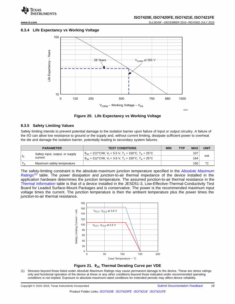
8.3.4 Life Expectancy vs Working Voltage
Figure 20. Life Expectancy vs Working Voltage
8.3.5 Safety Limiting ValuesSafety limiting intends to prevent potential damage to the isolation barrier upon failure of input or output circuitry. A failure ofthe I/O can allow low resistance to ground or the supply and, without current limiting, dissipate sufficient power to overheatthe die and damage the isolation barrier, potentially leading to secondary system failures.
PARAMETER TEST CONDITIONS MIN TYP MAX UNITθJA = 212°C/W, VI = 5.5 V, TJ = 150°C, TA = 25°C 107Safety input, output, or supplyIS mAcurrent θJA = 212°C/W, VI = 3.6 V, TJ = 150°C, TA = 25°C 164
TS Maximum safety temperature 150 °C
The safety-limiting constraint is the absolute-maximum junction temperature specified in the Absolute MaximumRatings (1) table. The power dissipation and junction-to-air thermal impedance of the device installed in theapplication hardware determines the junction temperature. The assumed junction-to-air thermal resistance in theThermal Information table is that of a device installed in the JESD51-3, Low-Effective-Thermal-Conductivity TestBoard for Leaded Surface-Mount Packages and is conservative. The power is the recommended maximum inputvoltage times the current. The junction temperature is then the ambient temperature plus the power times thejunction-to-air thermal resistance.
Figure 21. θJC Thermal Derating Curve per VDE(1) Stresses beyond those listed under Absolute Maximum Ratings may cause permanent damage to the device. These are stress ratings
only and functional operation of the device at these or any other conditions beyond those indicated under recommended operatingconditions is not implied. Exposure to absolute-maximum-rated conditions for extended periods may affect device reliability.
Copyright © 2010–2015, Texas Instruments Incorporated Submit Documentation Feedback 19
Product Folder Links: ISO7420E ISO7420FE ISO7421E ISO7421FE

IN
1 MW
500 W
ISO742xFx Input
VCCI
OUT
8 W
13 W
Output
VCCO
VCCI
IN
1 MW
500 W
ISO742xE Input
VCCI VCCIVCCI
ISO7420E, ISO7420FE, ISO7421E, ISO7421FESLLSE45F –DECEMBER 2010–REVISED JULY 2015 www.ti.com
8.4 Device Functional Modes
Table 2. Functional Table (1)
OUTPUTINPUT OUTA, OUTBVCCI VCCO INA, INB
ISO7420E / ISO7421E ISO7420FE / ISO7421FEH H H
PU PU L L LOpen H (2) L (3)
PD PU X H (2) L (3)
X PD X Undetermined Undetermined
(1) VCCI = Input-side VCC; VCCO = Output-side VCC; PU = Powered up (VCC ≥ 3 V); PD = Powered down (VCC ≤ 2.1 V); X = Irrelevant; H =High level; L = Low level;
(2) In fail-safe condition, output defaults to high level(3) In fail-safe condition, output defaults to low level
8.4.1 Device I/O Schematic
Figure 22. Device I/O Schematics
20 Submit Documentation Feedback Copyright © 2010–2015, Texas Instruments Incorporated
Product Folder Links: ISO7420E ISO7420FE ISO7421E ISO7421FE

ISO7421
VCC1
VCC2
ISO7420E, ISO7420FE, ISO7421E, ISO7421FEwww.ti.com SLLSE45F –DECEMBER 2010–REVISED JULY 2015
9 Applications and Implementation
NOTEInformation in the following applications sections is not part of the TI componentspecification, and TI does not warrant its accuracy or completeness. TI’s customers areresponsible for determining suitability of components for their purposes. Customers shouldvalidate and test their design implementation to confirm system functionality.
9.1 Application InformationISO742x utilize single-ended TTL-logic switching technology. Its supply voltage range is from 3 V to 5.5 V forboth supplies, VCC1 and VCC2. When designing with digital isolators, it is important to keep in mind that due to thesingle-ended design structure, digital isolators do not conform to any specific interface standard and are onlyintended for isolating single-ended CMOS or TTL digital signal lines. The isolator is typically placed between thedata controller (i.e. μC or UART), and a data converter or a line transceiver, regardless of the interface type orstandard.
9.2 Typical ApplicationISO7421 can be used with Texas Instruments' mixed signal micro-controller, digital-to-analog converter,transformer driver, and voltage regulator to create an isolated 4-20 mA current loop.
Figure 23. Isolated 4-20 mA Current Loop
Copyright © 2010–2015, Texas Instruments Incorporated Submit Documentation Feedback 21
Product Folder Links: ISO7420E ISO7420FE ISO7421E ISO7421FE

ISO7420E, ISO7420FE, ISO7421E, ISO7421FESLLSE45F –DECEMBER 2010–REVISED JULY 2015 www.ti.com
Typical Application (continued)9.2.1 Design RequirementsUnlike optocouplers, which require external components to improve performance, provide bias, or limit current,the ISO742x only require two external bypass capacitors to operate.
9.2.2 Detailed Design Procedure
9.2.2.1 Maximum Supply Current Equations(Calculated over recommended operating temperature range and Silicon process variation)
9.2.2.1.1 ISO7420
At VCC1 = VCC2 = 3.3V ± 10%ICC1(max) = ICC1_Q (max) + 1.791 x 10⁻² x f (1)ICC2(max) = ICC2_Q (max) + 1.687 x 10⁻² x f + 3.570 x 10⁻³ x f x CL (2)
At VCC1 = VCC2 = 5V ± 10%ICC1(max) = ICC1_Q (max) + 3.152 x 10⁻² x f (3)ICC2(max) = ICC2_Q (max) + 2.709 x 10⁻² x f + 5.365 x 10⁻³ x f x CL (4)
9.2.2.1.2 ISO7421
At VCC1 = VCC2 = 3.3V ± 10%ICC1(max) = ICC1_Q (max) + 1.726 x 10⁻² x f + 1.785 x 10⁻³ x f x CL (5)ICC2(max) = ICC2_Q (max) + 1.726 x 10⁻² x f + 1.785 x 10⁻³ x f x CL (6)
At VCC1 = VCC2 = 5V ± 10%ICC1(max) = ICC1_Q (max) + 2.920 x 10⁻² x f + 2.682 x 10⁻³ x f x CL (7)ICC2(max) = ICC2_Q (max) + 2.920 x 10⁻² x f + 2.682 x 10⁻³ x f x CL (8)
ICC1_Q (max) and ICC2_Q (max) are equivalent to the maximum supply currents measured in mA under DC inputconditions (provided in the specification tables of this data sheet); f is data rate in Mbps of both channels; CL isthe capacitive load in pF of both channels. ICC1(max) and ICC2(max) are measured in mA.
9.2.2.2 Typical Supply Current Equations:(Calculated over recommended operating temperature range and Silicon process variation)
9.2.2.2.1 ISO7420
At VCC1 = VCC2 = 3.3VICC1(typ) = ICC1_Q (typ) + 1.528 x 10⁻² x f (9)ICC2(typ) = ICC2_Q (typ) + 1.637 x 10⁻² x f + 3.275 x 10⁻³ x f x CL (10)
At VCC1 = VCC2 = 5VICC1(typ) = ICC1_Q (typ) + 2.640 x 10⁻² x f (11)ICC2(typ) = ICC2_Q (typ) + 2.502 x 10⁻² x f + 4.919 x 10⁻³ x f x CL (12)
9.2.2.2.2 ISO7421
At VCC1 = VCC2 = 3.3VICC1(typ) = ICC1_Q (typ) + 1.567 x 10⁻² x f + 1.640 x 10⁻³ x f x CL (13)ICC2(typ) = ICC2_Q (typ) + 1.567 x 10⁻² x f + 1.640 x 10⁻³ x f x CL (14)
At VCC1 = VCC2 = 5VICC1(typ) = ICC1_Q (typ) + 2.550 x 10⁻² x f + 2.416 x 10⁻³ x f x CL (15)ICC2(typ) = ICC2_Q (typ) + 2.550 x 10⁻² x f + 2.461 x 10⁻³ x f x CL (16)
22 Submit Documentation Feedback Copyright © 2010–2015, Texas Instruments Incorporated
Product Folder Links: ISO7420E ISO7420FE ISO7421E ISO7421FE

1
2
3
4
8
7
6
5
INA
INB
OUTA
OUTB
VCC2
0.1 µF
GND2
0.1 µF
VCC1
GND1
1
2
3
4
8
7
6
5
INA
INB
OUTA
VCC2
0.1 µF
GND2
0.1 µF
VCC1
OUTB
GND1
ISO7420E, ISO7420FE, ISO7421E, ISO7421FEwww.ti.com SLLSE45F –DECEMBER 2010–REVISED JULY 2015
Typical Application (continued)ICC1_Q (typ) and ICC2_Q (typ) are equivalent to the typical supply currents measured in mA under DC inputconditions (provided in the specification tables of this data sheet); f is data rate in Mbps of each channel; CL isthe capacitive load in pF of each channel. ICC1(typ) and ICC2(typ) are measured in mA.
Figure 24. Typical ISO7420 Circuit Hookup
Figure 25. Typical ISO7421 Circuit Hookup
Copyright © 2010–2015, Texas Instruments Incorporated Submit Documentation Feedback 23
Product Folder Links: ISO7420E ISO7420FE ISO7421E ISO7421FE

T = 25°C, V = V = 3.3 V,A CC1 CC2 Pattern: PRBS 2 -17 T = 25°C, V 1 = V 2 = 3.3 V, Pattern: PRBS 2 -1A CC CC7
ISO7420E, ISO7420FE, ISO7421E, ISO7421FESLLSE45F –DECEMBER 2010–REVISED JULY 2015 www.ti.com
Typical Application (continued)9.2.3 Application Curves
Figure 27. ISO7420FE Typical Eye Diagram at 100 MBPS,Figure 26. ISO7420FE Typical Eye Diagram at 50 MBPS,3.3 V Operation3.3 V Operation
10 Power Supply RecommendationsTo ensure reliable operation at all data rates and supply voltages, a 0.1 µF bypass capacitor is recommended atinput and output supply pins (VCC1 and VCC2). The capacitors should be placed as close to the supply pins aspossible. If only a single primary-side power supply is available in an application, isolated power can begenerated for the secondary-side with the help of a transformer driver such as Texas Instruments' SN6501. Forsuch applications, detailed power supply design and transformer selection recommendations are available inSN6501 datasheet (SLLSEA0).
24 Submit Documentation Feedback Copyright © 2010–2015, Texas Instruments Incorporated
Product Folder Links: ISO7420E ISO7420FE ISO7421E ISO7421FE

10 mils
10 mils
40 milsFR-4
0r ~ 4.5
Keep this space free
from planes,traces , pads,
and vias
Ground plane
Power plane
Low-speed traces
High-speed traces
ISO7420E, ISO7420FE, ISO7421E, ISO7421FEwww.ti.com SLLSE45F –DECEMBER 2010–REVISED JULY 2015
11 Layout
11.1 Layout GuidelinesA minimum of four layers is required to accomplish a low EMI PCB design (see Figure 28). Layer stacking shouldbe in the following order (top-to-bottom): high-speed signal layer, ground plane, power plane and low-frequencysignal layer.• Routing the high-speed traces on the top layer avoids the use of vias (and the introduction of their
inductances) and allows for clean interconnects between the isolator and the transmitter and receiver circuitsof the data link.
• Placing a solid ground plane next to the high-speed signal layer establishes controlled impedance fortransmission line interconnects and provides an excellent low-inductance path for the return current flow.
• Placing the power plane next to the ground plane creates additional high-frequency bypass capacitance ofapproximately 100pF/in2.
• Routing the slower speed control signals on the bottom layer allows for greater flexibility as these signal linksusually have margin to tolerate discontinuities such as vias.
If an additional supply voltage plane or signal layer is needed, add a second power / ground plane system to thestack to keep it symmetrical. This makes the stack mechanically stable and prevents it from warping. Also thepower and ground plane of each power system can be placed closer together, thus increasing the high-frequencybypass capacitance significantly.
For detailed layout recommendations, see Application Note Digital Isolator Design Guide, SLLA284.
11.1.1 PCB MaterialFor digital circuit boards operating below 150 Mbps, (or rise and fall times higher than 1 ns), and trace lengths ofup to 10 inches, use standard FR-4 epoxy-glass as PCB material. FR-4 (Flame Retardant 4) meets therequirements of Underwriters Laboratories UL94-V0, and is preferred over cheaper alternatives due to its lowerdielectric losses at high frequencies, less moisture absorption, greater strength and stiffness, and its self-extinguishing flammability-characteristics.
11.2 Layout Example
Figure 28. Recommended Layer Stack
Copyright © 2010–2015, Texas Instruments Incorporated Submit Documentation Feedback 25
Product Folder Links: ISO7420E ISO7420FE ISO7421E ISO7421FE
ISO7420E, ISO7420FE, ISO7421E, ISO7421FESLLSE45F –DECEMBER 2010–REVISED JULY 2015 www.ti.com
12 Device and Documentation Support
12.1 Documentation Support
12.1.1 Related DocumentationFor related documentation see the following:• SN6501 Transformer Driver for Isolated Power Supplies, SLLSEA0• Isolation Glossary, SLLS353
12.2 Related LinksThe table below lists quick access links. Categories include technical documents, support and communityresources, tools and software, and quick access to sample or buy.
Table 3. Related LinksTECHNICAL TOOLS & SUPPORT &PARTS PRODUCT FOLDER SAMPLE & BUY DOCUMENTS SOFTWARE COMMUNITY
ISO7420E Click here Click here Click here Click here Click hereISO7420FE Click here Click here Click here Click here Click hereISO7421E Click here Click here Click here Click here Click here
ISO7421FE Click here Click here Click here Click here Click here
12.3 Community ResourcesThe following links connect to TI community resources. Linked contents are provided "AS IS" by the respectivecontributors. They do not constitute TI specifications and do not necessarily reflect TI's views; see TI's Terms ofUse.
TI E2E™ Online Community TI's Engineer-to-Engineer (E2E) Community. Created to foster collaborationamong engineers. At e2e.ti.com, you can ask questions, share knowledge, explore ideas and helpsolve problems with fellow engineers.
Design Support TI's Design Support Quickly find helpful E2E forums along with design support tools andcontact information for technical support.
12.4 TrademarksDeviceNet, E2E are trademarks of Texas Instruments.All other trademarks are the property of their respective owners.
12.5 Electrostatic Discharge CautionThese devices have limited built-in ESD protection. The leads should be shorted together or the device placed in conductive foamduring storage or handling to prevent electrostatic damage to the MOS gates.
12.6 GlossarySLYZ022 — TI Glossary.
This glossary lists and explains terms, acronyms, and definitions.
13 Mechanical, Packaging, and Orderable InformationThe following pages include mechanical, packaging, and orderable information. This information is the mostcurrent data available for the designated devices. This data is subject to change without notice and revision ofthis document. For browser-based versions of this data sheet, refer to the left-hand navigation.
26 Submit Documentation Feedback Copyright © 2010–2015, Texas Instruments Incorporated
Product Folder Links: ISO7420E ISO7420FE ISO7421E ISO7421FE

PACKAGE OPTION ADDENDUM
www.ti.com 21-May-2013
Addendum-Page 1
PACKAGING INFORMATION
Orderable Device Status(1)
Package Type PackageDrawing
Pins PackageQty
Eco Plan(2)
Lead/Ball Finish MSL Peak Temp(3)
Op Temp (°C) Device Marking(4/5)
Samples
ISO7420ED ACTIVE SOIC D 8 75 Green (RoHS& no Sb/Br)
CU NIPDAU Level-1-260C-UNLIM -40 to 125 SO7420
ISO7420EDR ACTIVE SOIC D 8 2500 Green (RoHS& no Sb/Br)
CU NIPDAU Level-1-260C-UNLIM -40 to 125 SO7420
ISO7420FED ACTIVE SOIC D 8 75 Green (RoHS& no Sb/Br)
CU NIPDAU Level-1-260C-UNLIM -40 to 125 I7420F
ISO7420FEDR ACTIVE SOIC D 8 2500 Green (RoHS& no Sb/Br)
CU NIPDAU Level-1-260C-UNLIM -40 to 125 I7420F
ISO7421ED ACTIVE SOIC D 8 75 Green (RoHS& no Sb/Br)
CU NIPDAU Level-1-260C-UNLIM -40 to 125 SO7421
ISO7421EDR ACTIVE SOIC D 8 2500 Green (RoHS& no Sb/Br)
CU NIPDAU Level-1-260C-UNLIM -40 to 125 SO7421
ISO7421FED ACTIVE SOIC D 8 75 Green (RoHS& no Sb/Br)
CU NIPDAU Level-1-260C-UNLIM -40 to 125 I7421F
ISO7421FEDR ACTIVE SOIC D 8 2500 Green (RoHS& no Sb/Br)
CU NIPDAU Level-1-260C-UNLIM -40 to 125 I7421F
(1) The marketing status values are defined as follows:ACTIVE: Product device recommended for new designs.LIFEBUY: TI has announced that the device will be discontinued, and a lifetime-buy period is in effect.NRND: Not recommended for new designs. Device is in production to support existing customers, but TI does not recommend using this part in a new design.PREVIEW: Device has been announced but is not in production. Samples may or may not be available.OBSOLETE: TI has discontinued the production of the device.
(2) Eco Plan - The planned eco-friendly classification: Pb-Free (RoHS), Pb-Free (RoHS Exempt), or Green (RoHS & no Sb/Br) - please check http://www.ti.com/productcontent for the latest availabilityinformation and additional product content details.TBD: The Pb-Free/Green conversion plan has not been defined.Pb-Free (RoHS): TI's terms "Lead-Free" or "Pb-Free" mean semiconductor products that are compatible with the current RoHS requirements for all 6 substances, including the requirement thatlead not exceed 0.1% by weight in homogeneous materials. Where designed to be soldered at high temperatures, TI Pb-Free products are suitable for use in specified lead-free processes.Pb-Free (RoHS Exempt): This component has a RoHS exemption for either 1) lead-based flip-chip solder bumps used between the die and package, or 2) lead-based die adhesive used betweenthe die and leadframe. The component is otherwise considered Pb-Free (RoHS compatible) as defined above.Green (RoHS & no Sb/Br): TI defines "Green" to mean Pb-Free (RoHS compatible), and free of Bromine (Br) and Antimony (Sb) based flame retardants (Br or Sb do not exceed 0.1% by weightin homogeneous material)
(3) MSL, Peak Temp. -- The Moisture Sensitivity Level rating according to the JEDEC industry standard classifications, and peak solder temperature.

PACKAGE OPTION ADDENDUM
www.ti.com 21-May-2013
Addendum-Page 2
(4) There may be additional marking, which relates to the logo, the lot trace code information, or the environmental category on the device.
(5) Multiple Device Markings will be inside parentheses. Only one Device Marking contained in parentheses and separated by a "~" will appear on a device. If a line is indented then it is a continuationof the previous line and the two combined represent the entire Device Marking for that device.
Important Information and Disclaimer:The information provided on this page represents TI's knowledge and belief as of the date that it is provided. TI bases its knowledge and belief on informationprovided by third parties, and makes no representation or warranty as to the accuracy of such information. Efforts are underway to better integrate information from third parties. TI has taken andcontinues to take reasonable steps to provide representative and accurate information but may not have conducted destructive testing or chemical analysis on incoming materials and chemicals.TI and TI suppliers consider certain information to be proprietary, and thus CAS numbers and other limited information may not be available for release.
In no event shall TI's liability arising out of such information exceed the total purchase price of the TI part(s) at issue in this document sold by TI to Customer on an annual basis.
OTHER QUALIFIED VERSIONS OF ISO7421E :
• Automotive: ISO7421E-Q1
NOTE: Qualified Version Definitions:
• Automotive - Q100 devices qualified for high-reliability automotive applications targeting zero defects

TAPE AND REEL INFORMATION
*All dimensions are nominal
Device PackageType
PackageDrawing
Pins SPQ ReelDiameter
(mm)
ReelWidth
W1 (mm)
A0(mm)
B0(mm)
K0(mm)
P1(mm)
W(mm)
Pin1Quadrant
ISO7420EDR SOIC D 8 2500 330.0 12.4 6.4 5.2 2.1 8.0 12.0 Q1
ISO7420FEDR SOIC D 8 2500 330.0 12.4 6.4 5.2 2.1 8.0 12.0 Q1
ISO7421EDR SOIC D 8 2500 330.0 12.4 6.4 5.2 2.1 8.0 12.0 Q1
ISO7421FEDR SOIC D 8 2500 330.0 12.4 6.4 5.2 2.1 8.0 12.0 Q1
PACKAGE MATERIALS INFORMATION
www.ti.com 24-Aug-2016
Pack Materials-Page 1

*All dimensions are nominal
Device Package Type Package Drawing Pins SPQ Length (mm) Width (mm) Height (mm)
ISO7420EDR SOIC D 8 2500 367.0 367.0 38.0
ISO7420FEDR SOIC D 8 2500 367.0 367.0 38.0
ISO7421EDR SOIC D 8 2500 367.0 367.0 38.0
ISO7421FEDR SOIC D 8 2500 367.0 367.0 38.0
PACKAGE MATERIALS INFORMATION
www.ti.com 24-Aug-2016
Pack Materials-Page 2


IMPORTANT NOTICE
Texas Instruments Incorporated and its subsidiaries (TI) reserve the right to make corrections, enhancements, improvements and otherchanges to its semiconductor products and services per JESD46, latest issue, and to discontinue any product or service per JESD48, latestissue. Buyers should obtain the latest relevant information before placing orders and should verify that such information is current andcomplete. All semiconductor products (also referred to herein as “components”) are sold subject to TI’s terms and conditions of salesupplied at the time of order acknowledgment.TI warrants performance of its components to the specifications applicable at the time of sale, in accordance with the warranty in TI’s termsand conditions of sale of semiconductor products. Testing and other quality control techniques are used to the extent TI deems necessaryto support this warranty. Except where mandated by applicable law, testing of all parameters of each component is not necessarilyperformed.TI assumes no liability for applications assistance or the design of Buyers’ products. Buyers are responsible for their products andapplications using TI components. To minimize the risks associated with Buyers’ products and applications, Buyers should provideadequate design and operating safeguards.TI does not warrant or represent that any license, either express or implied, is granted under any patent right, copyright, mask work right, orother intellectual property right relating to any combination, machine, or process in which TI components or services are used. Informationpublished by TI regarding third-party products or services does not constitute a license to use such products or services or a warranty orendorsement thereof. Use of such information may require a license from a third party under the patents or other intellectual property of thethird party, or a license from TI under the patents or other intellectual property of TI.Reproduction of significant portions of TI information in TI data books or data sheets is permissible only if reproduction is without alterationand is accompanied by all associated warranties, conditions, limitations, and notices. TI is not responsible or liable for such altereddocumentation. Information of third parties may be subject to additional restrictions.Resale of TI components or services with statements different from or beyond the parameters stated by TI for that component or servicevoids all express and any implied warranties for the associated TI component or service and is an unfair and deceptive business practice.TI is not responsible or liable for any such statements.Buyer acknowledges and agrees that it is solely responsible for compliance with all legal, regulatory and safety-related requirementsconcerning its products, and any use of TI components in its applications, notwithstanding any applications-related information or supportthat may be provided by TI. Buyer represents and agrees that it has all the necessary expertise to create and implement safeguards whichanticipate dangerous consequences of failures, monitor failures and their consequences, lessen the likelihood of failures that might causeharm and take appropriate remedial actions. Buyer will fully indemnify TI and its representatives against any damages arising out of the useof any TI components in safety-critical applications.In some cases, TI components may be promoted specifically to facilitate safety-related applications. With such components, TI’s goal is tohelp enable customers to design and create their own end-product solutions that meet applicable functional safety standards andrequirements. Nonetheless, such components are subject to these terms.No TI components are authorized for use in FDA Class III (or similar life-critical medical equipment) unless authorized officers of the partieshave executed a special agreement specifically governing such use.Only those TI components which TI has specifically designated as military grade or “enhanced plastic” are designed and intended for use inmilitary/aerospace applications or environments. Buyer acknowledges and agrees that any military or aerospace use of TI componentswhich have not been so designated is solely at the Buyer's risk, and that Buyer is solely responsible for compliance with all legal andregulatory requirements in connection with such use.TI has specifically designated certain components as meeting ISO/TS16949 requirements, mainly for automotive use. In any case of use ofnon-designated products, TI will not be responsible for any failure to meet ISO/TS16949.
Products ApplicationsAudio www.ti.com/audio Automotive and Transportation www.ti.com/automotiveAmplifiers amplifier.ti.com Communications and Telecom www.ti.com/communicationsData Converters dataconverter.ti.com Computers and Peripherals www.ti.com/computersDLP® Products www.dlp.com Consumer Electronics www.ti.com/consumer-appsDSP dsp.ti.com Energy and Lighting www.ti.com/energyClocks and Timers www.ti.com/clocks Industrial www.ti.com/industrialInterface interface.ti.com Medical www.ti.com/medicalLogic logic.ti.com Security www.ti.com/securityPower Mgmt power.ti.com Space, Avionics and Defense www.ti.com/space-avionics-defenseMicrocontrollers microcontroller.ti.com Video and Imaging www.ti.com/videoRFID www.ti-rfid.comOMAP Applications Processors www.ti.com/omap TI E2E Community e2e.ti.comWireless Connectivity www.ti.com/wirelessconnectivity
Mailing Address: Texas Instruments, Post Office Box 655303, Dallas, Texas 75265Copyright © 2016, Texas Instruments Incorporated