low-power,highly-integrated… · 1 2 3 4 5 6 7 8 9 10 11 12 13 14 15 30 29 28 27 26 25 24 23 22 21...
TRANSCRIPT

www.ti.com
FEATURES
APPLICATIONS
TLV320AIC12, TLV320AIC13TLV320AIC14, TLV320AIC15
TLV320AIC12K, TLV320AIC14KSLWS115E–OCTOBER 2001–REVISED JANUARY 2007
LOW-POWER, HIGHLY-INTEGRATED, PROGRAMMABLE16-Bit, 26-KSPS MONO CODEC
– Analog and Digital Sidetone• Mono 16-Bit Oversampling Sigma-Delta A/D – Antialiasing Filter (AAF)
Converter – Programmable Input and Output Gain• Mono 16-Bit Oversampling Sigma-Delta D/A Control (PGA)
Converter – Microphone/Handset/Headset Amplifiers• Support Maximum Master Clock of 100 MHz to – AIC12K has an 8-Ω Speaker Driver
Allow the DSP Output Clock to be Used as a – Power Management WithMaster Clock Hardware/Software Power-Down Modes
• Selectable FIR/IIR Filter With Bypassing 30 µWOption • Separate Software Control for ADC and DAC
• Programmable Sampling Rate up to: Power Down– Max 26 Ksps With On-Chip IIR/FIR Filter • Fully Compatible With Common TMS320™– Max 104 Ksps With IIR/FIR Bypassed DSP Family and Microcontroller Power
Supplies• On-Chip FIR Produced 84-dB SNR for ADCand 92-dB SNR for DAC – 1.65 V - 1.95 V Digital Core Power
• Smart Time Division Multiplexed – 1.1 V - 3.6 V Digital I/O(SMARTDM™) Serial Port – 2.7 V - 3.6 V Analog– Glueless 4-Wire Interface to DSP • Power Dissipation (PD)– Automatic Cascade Detection (ACD) – 11.2 mW at 3.3 V in Standard Operation
Self-Generates Master/Slave Device – 17.8 mW at 3.3 V With Headphone DriversAddresses
• Internal Reference Voltage (Vref)– Programming Mode to Allow On-the-Fly• 2s Complement Data FormatReconfiguration• Test Modes Which Include Digital Loopback– Continuous Data Transfer Mode to
and Analog LoopbackMinimize Bit Clock Speed– Support Different Sampling Rate for Each
Device • Digital Still Cameras– Turbo Mode to Maximize Bit Clock for • Wireless Accessories
Faster Data Transfer and Allow Multiple• Hands-Free Car KitsSerial Devices to Share the Same Bus• VOIP
– Allows up to 16 Devices to be Connected• Cable Modemto a Single Serial Port
• Host Port– 2-Wire Interface– Selectable I2C or S2C
• Differential and Single-Ended AnalogInput/Output
• Built-In Analog Functions:
Please be aware that an important notice concerning availability, standard warranty, and use in critical applications of TexasInstruments semiconductor products and disclaimers thereto appears at the end of this data sheet.
SMARTDM, TMS320C5000, TMS320C6000 are trademarks of Texas Instruments.TMS320 is a trademark of Texas Instrument.
PRODUCTION DATA information is current as of publication date. Copyright © 2001–2007, Texas Instruments IncorporatedProducts conform to specifications per the terms of the TexasInstruments standard warranty. Production processing does notnecessarily include testing of all parameters.

www.ti.com
DESCRIPTION
TLV320AIC12, TLV320AIC13TLV320AIC14, TLV320AIC15TLV320AIC12K, TLV320AIC14KSLWS115E–OCTOBER 2001–REVISED JANUARY 2007
These devices have limited built-in ESD protection. The leads should be shorted together or the device placed in conductive foamduring storage or handling to prevent electrostatic damage to the MOS gates.
The TLV320AIC1x is a true low-cost, low-power, high-integrated, high-performance, mono voice codec. Itfeatures one 16-bit analog-to-digital (A/D) channel and one 16-bit digital-to-analog (D/A) channel.
The TLV320AIC1x provides high-resolution signal conversion from digital-to-analog (D/A) and fromanalog-to-digital (A/D) using oversampling sigma-delta technology with programmable sampling rate.
The TLV320AIC1x implements the smart time division multiplexed serial port (SMARTDM™). The SMARTDMport is a synchronous 4-wire serial port in TDM format for glue-free interface to TI DSPs (i.e. TMS320C5000™,TMS320C6000™) and microcontrollers. The SMARTDM supports both continuous data transfer mode andon-the-fly reconfiguration programming mode. The TLV320AIC1x can be gluelessly cascaded to anySMARTDM-based device to form multichannel codec and up to 16 TLV320AIC1x codecs can be cascaded to asingle serial port.
The TLV320AIC1x also provides a flexible host port. The host port interface is a two-wire serial interface thatcan be programmed to be either an industrial standard I2C or a simple S2C (start-stop communication protocol).
The TLV320AIC1x also integrates all of the critical functions needed for most voice-band applications includingMIC preamplifier, handset amplifier, headset amplifier, antialiasing filter (AAF), input/output programmable gainamplifier (PGA), and selectable low-pass IIR/FIR filters. The AIC12K also includes an 8-Ω speaker driver.
The TLV320AIC1x implements an extensive power management; including device power-down, independentsoftware control for turning off ADC, DAC, operational-amplifiers, and IIR/FIR filter (bypass) to maximize systempower conservation. The TLV320AIC1x consumes only 11.2 mW at 3.3 V.
The TLV320AIC1x low power operation from 2.7 V to 3.6 V power supplies, along with extensive powermanagement, make it ideal for portable applications including wireless accessories, hands free car kits, VOIP,cable modem, and speech processing. Its low group delay characteristic makes it suitable for single ormultichannel active control applications.
The TLV320AIC1x is characterized for commercial operation from 0°C to 70°C and industrial operation from-40°C to 85°C. The TLV320AIC1xk is characterized for industrial operation from -40°C to 85°C.
ORDERING INFORMATION
OPERATINGPACKAGE ORDERING TRANSPORT MEDIA,PRODUCT PACKAGE (1) TEMPERATUREDESIGNATOR NUMBER QUANTITYRANGE, TA
TLV320AIC1xCDBT Tape and Reel, 250TLV320AIC1xC TSSOP-30 DBT 0°C to 70°C
TLV320AIC1xCDBTR Tape and Reel, 3000
TLV320AIC1xIDBT Tape and Reel, 250TLV320AIC1xI TSSOP-30 DBT -40°C to 85°C
TLV320AIC1xIDBTR Tape and Reel, 3000
TLV320AIC12KIRHBT Tape and Reel, 250TLV320AIC12K QFN-32 RHB -40°C to 85°C
TLV320AIC12KIRHBR Tape and Reel, 3000
TLV320AIC14KIRHBT Tape and Reel, 250TLV320AIC14K QFN-32 RHB -40°C to 85°C
TLV320AIC14KIRHBR Tape and Reel, 3000
(1) For the most current package and ordering information, see the Package Option Addendum at the end of this document, or see the TIWeb site at www.ti.com.
2 Submit Documentation Feedback

www.ti.com
123
4 56789
101112131415
302928
272625242322
212019181716
IOVSSIOVDD
FSDFS
DOUTDINM/S
PWRDNOUTM1OUTP1DRVDDDRVSSOUTP2OUTMVOUTP3
DVSSDVDDSCLKSDASCLMCLKRESETINP1INM1BIASINM2INP2MICINAVDDAVSS
123
4 56789
101112131415
302928
272625242322
212019181716
IOVSSIOVDD
FSDFS
DOUTDINM/S
PWRDNOUTM1OUTP1DRVDDDRVSS
NCNCNC
DVSSDVDDSCLKSDASCLMCLKRESETINP1INM1BIASINM2INP2MICINAVDDAVSS
1 2 3 4 5 6 7 8
9
10
11
12
13
14
15
31
29
28
27
26
25
24 23 22 21 20 19 18 17
16
IOV
SS
IOV
DD
FS
D
FS
DOUT
DIN
M/S
PWRDN
OUTM1
N/C
N/C DRVDD
DR
VS
S
N/C
N/C
N/C
DV
SS
DV
DD
SC
LK
SD
A
SCL
MCLK
RESET
INP1
INM1
BIAS
INM2IN
P2
MIC
IN
AV
SS
AV
DD
OUTP1
30
31
1 2 3 4 5 6 7 8
9
10
11
12
13
14
15
31
29
28
27
26
25
24 23 22 21 20 19 18 17
16
IOV
SS
IOV
DD
FS
D
FS
DOUT
DIN
M/S
PWRDN
OUTM1
N/C
N/C DRVDD
DR
VS
S
OU
TP
2
OU
TM
V
OU
TP
3
DV
SS
DV
DD
SC
LK
SD
A
SCL
MCLK
RESET
INP1
INM1
BIAS
INM2
INP
2
MIC
IN
AV
SS
AV
DD
OUTP1
30
31
TLV320AIC12, TLV320AIC13TLV320AIC14, TLV320AIC15
TLV320AIC12K, TLV320AIC14KSLWS115E–OCTOBER 2001–REVISED JANUARY 2007
AIC12/13/12K DBT PACKAGE AIC14/15/14K DBT PACKAGE(TOP VIEW) (TOP VIEW)
AIC12K RHB PACKAGE AIC14K RHB PACKAGE(TOP VIEW) (TOP VIEW)
NOTE: For the RHB package, connect the device thermal pad to DRVDD.
3Submit Documentation Feedback

www.ti.com
TLV320AIC12, TLV320AIC13TLV320AIC14, TLV320AIC15TLV320AIC12K, TLV320AIC14KSLWS115E–OCTOBER 2001–REVISED JANUARY 2007
Terminal FunctionsTERMINAL
NAME AIC12/13/12K AIC14/15/14K AIC12K AIC14K I/O DESCRIPTIONDBT DBT RHB RHBNO. NO. NO. NO.
IOVSS 1 1 5 5 I Digital I/O ground
IOVDD 2 2 6 6 I Digital I/O power supply
Frame sync delayed output. The FSD output synchronizes a slavedevice to the frame sync of the master device. FSD is applied to theslave FS input and is the same duration as the master FS signal. ThisFSD 3 3 7 7 O pin must be pulled low if AIC1x is a stand-alone slave. It must bepulled high if the AIC1x is a stand-alone master or the last slave in thecascade.
Frame sync. When FS goes low, DIN begins receiving data bits andFS 4 4 8 8 I/O DOUT begins transmitting data bits. In master mode, FS is internally
generated. In slave mode, FS is externally generated.
Data output. DOUT transmits the ADC output bits and registers data,DOUT 5 5 9 9 O and is synchronized to SCLK and FS. Data is sent out at the rising
edge of SCLK. Outside data/control frame, DOUT is put in 3-state.
Data input. DIN receives the DAC input data and register data from theDIN 6 6 10 10 I external DSP (digital signal processor) and is synchronized to SCLK
and FS. Data is latched at the falling edge of SCLK.
Master/slave select input. When M/S is high, the device is the master,M/S 7 7 11 11 I and when low it is a slave.
Power down. When PWRDN is pulled low, the device goes into apower-down mode, the serial interface is disabled, and most of thehigh-speed clocks are disabled. However, all the register values arePWRDN 8 8 12 12 I sustained and the device resumes full-power operation withoutreinitialization when PWRDN is pulled high again. PWRDN resets thecounters only and preserves the programmed register contents.
Inverting output of the DAC. OUTM1 is functionally identical with andcomplementary to OUTP1. This differential output can drive aOUTM1 9 9 13 13 O maximum load of 600 Ω. This output can also be used alone forsingle-ended operation.
Noninverting output of the DAC. This differential output can drive aOUTP1 10 10 14 14 O maximum load of 600 Ω. This output can also be used alone for
single-ended operation.
DRVDD 11 11 15 15 I Analog power supply for the 16-Ω drivers OUTP2 and OUTP3
DRVSS 12 12 17 17 I Analog ground for the 16-Ω drivers OUTP2 and OUTP3
Analog output number 2 from the 16-Ω driver. This output can drive aOUTP2 13 – 18 – O maximum load of 16 Ω, and also can be configured as either
single-ended output or differential output by the control register 6.
Programmable virtual ground for the output of OUTP2 and OUTP3OUTMV 14 – 19 – O (see the Register Map).
Analog output number 3 from the 16-Ω driver. This output can drive aOUTP3 15 – 20 – O maximum load of 16 Ω, and also be configured as either single-ended
output or differential output by the control register 6.
AVSS 16 16 21 21 I Analog ground
AVDD 17 17 22 22 I Analog power supply
MICIN 18 18 23 23 I MIC preamplifier input. It must be connected to AVSS if not used.
INP2 19 19 24 24 I Noninverting analog input 2. It must be connected to AVSS if not used.
INM2 20 20 25 25 I Inverting analog input 2. It must be connected to AVSS if not used.
Bias output voltage is software selectable between 1.35 V and 2.35 V.BIAS 21 21 27 27 O Its output current is 5 mA.
INM1 22 22 28 28 I Inverting analog input 1. It must be connected to AVSS if not used.
INP1 23 23 29 29 I Noninverting analog input 1. It must be connected to AVSS if not used.
Hardware reset. The reset function is provided to initialize all of theRESET 24 24 30 30 I internal registers to their default values. The serial port is configured to
the default state accordingly.
Master clock. MCLK derives the internal clocks of the sigma-deltaMCLK 25 25 31 31 I analog interface circuit.
SCL 26 26 32 32 I Programmable host port (I2C or S2C) clock input.
SDA 27 27 1 1 I/O Programmable host port (I2C or S2C) data line.
4 Submit Documentation Feedback

www.ti.com
Electrical Characteristics
Absolute Maximum Ratings
TLV320AIC12, TLV320AIC13TLV320AIC14, TLV320AIC15
TLV320AIC12K, TLV320AIC14KSLWS115E–OCTOBER 2001–REVISED JANUARY 2007
Terminal Functions (continued)TERMINAL
NAME AIC12/13/12K AIC14/15/14K AIC12K AIC14K I/O DESCRIPTIONDBT DBT RHB RHBNO. NO. NO. NO.
Shift clock. SCLK signal clocks serial data into DIN and out of DOUTduring the frame-sync interval. When configured as an output (M/Shigh), SCLK is generated internally by multiplying the frame-sync signal
SCLK 28 28 2 2 I/O frequency by 16 and the number of codecs in cascade in standard andcontinuous mode. When configured as an input (M/S low), SCLK isgenerated externally and must be synchronous with the master clockand frame sync.
DVDD 29 29 3 3 I Digital power supply
DVSS 30 30 4 4 I Digital ground
16, 18, 19, 20,NC – 13, 14, 15 16, 26 No connection26
AIC12, AIC13, AIC14, AIC15, AIC12K, AIC14K: Over Recommended Operating Free-Air Temperature Range
AVDD = 3.3 V, DVDD = 1.8 V, IOVDD = 3.3 V (Unless Otherwise Noted)
Over Operating Free-Air Temperature Range (Unless Otherwise Noted) (1)
UNITS
VCC Supply voltage range: DVDD (2) -0.3 V to 2.25 V
AVDD, DRVDD, IOVDD (2) -0.3 V to 4 V
VO Output voltage range, all digital output signals -0.3 V to IOVDD + 0.3 V
VI Input voltage range, all digital input signals -0.3 V to IOVDD + 0.3 V
TA Operating free-air temperature range -40°C to 85°C
TJ Junction temperature 105°C
Tstg Storage temperature range -65°C to 150°C
Power dissipation (TJmax - TA ) / θJA
θJA Thermal impedance 44°C/W
Case temperature for 10 seconds: Package 260°C
AIC12, AIC13, AIC14, AIC15, AIC12k and AIC14k all CDM 500 Vpins
AIC12, AIC13, AIC14, AIC15, AIC12k and AIC14k all HBM 2 kVESD Characteristics pins except for the following:
DVDD, SDA HBM 1.3 kV
DOUT HBM 1.9 kV
(1) Stresses beyond those listed under absolute maximum ratings may cause permanent damage to the device. These are stress ratingsonly and functional operation of the device at these or any other conditions beyond those indicated under recommended operatingconditions is not implied. Exposure to absolute-maximum-rated conditions for extended periods may affect device reliability.
(2) All voltage values are with respect to VSS.
5Submit Documentation Feedback

www.ti.com
Recommended Operating Conditions
TLV320AIC12, TLV320AIC13TLV320AIC14, TLV320AIC15TLV320AIC12K, TLV320AIC14KSLWS115E–OCTOBER 2001–REVISED JANUARY 2007
MIN NOM MAX MIN NOM MAX UNIT
AIC12/13/14/15 AIC12K/14K
Supply voltage for analog, AVDD 2.7 3.3 3.6 2.7 3.3 3.6 V
Supply voltage for analog output driver, DRVDD 2.7 3.6 2.7 3.6VSS
Supply voltage for digital core, DVDD 1.65 1.8 1.95 1.65 1.8 1.95 V
Supply voltage for digital I/O, IOVDD 1.1 3.3 3.6 1.1 3.3 3.6 V
VI(analog) Analog single-ended peak-to-peak input voltage 2 2 V
Between OUTP1 and 600 600OUTM1 (differential)
Between OUTP2 and 16 16OUTMV (single-ended)
Between OUTP3 andRL Output load resistance, 16 16 ΩOUTMV (single-ended)
Between OUTP2 and 32 32OUTMV (differential)
Between OUTP3 and 32 32OUTMV (differential)
CL Analog output load capacitance 20 20 pF
Digital output capacitance 20 20 pF
Master clock 100 100 MHz
ADC or DAC conversion rate 26 26 kHz
TA Operating free-air temperature -40 85 -40 85 °C
6 Submit Documentation Feedback

www.ti.com
Digital Inputs and Outputs
ADC Path Filter
TLV320AIC12, TLV320AIC13TLV320AIC14, TLV320AIC15
TLV320AIC12K, TLV320AIC14KSLWS115E–OCTOBER 2001–REVISED JANUARY 2007
Fs = 8 kHz, Outputs Not Loaded
PARAMETER (1) MIN TYP MAX UNIT
VOH High-level output voltage, DOUT 0.8 IOVDD V
VOL Low-level output voltage, DOUT 0.1 IOVDD V
IIH High-level input current, any digital input 0.5 µA
IIL Low-level input current, any digital input 0.5 µA
CI Input capacitance 3 pF
Co Output capacitance 5 pF
(1) For VIH (Input high level), when IOVDD < 1.6 V, minimum VIH is 1.1V.
Fs = 8 KHz (1) (2)
TESTPARAMETER MIN TYP MAX MIN TYP MAX UNITCONDITIONS
FIR FILTER IIR FILTER
0 Hz to 30 Hz -0.5 0.2 -0.5 0.2
300 Hz to 3 Hz -0.5 0.25 -0.5 0.25
3.3 Hz -0.5 0.3 -1.5 0.3Filter gain relative to gain dBat 1020 Hz 3.6 KHz -3 -3
4 kHz -35 -20
≥ 4.4 KHz -74 -60
(1) The filter gain outside of the passband is measured with respect to the gain at 1020 Hz. The analog input test signal is a sine wave with0 dB = 4 VI(PP) as the reference level for the analog input signal. The pass band is 0 to 3600 Hz for an 8-KHz sample rate. This passband scales linearly with the sample rate.
(2) The filter characteristics are specified by design and are not tested in production.
7Submit Documentation Feedback

www.ti.com
ADC DYNAMIC PERFORMANCE
ADC CHANNEL CHARACTERISTICS
TLV320AIC12, TLV320AIC13TLV320AIC14, TLV320AIC15TLV320AIC12K, TLV320AIC14KSLWS115E–OCTOBER 2001–REVISED JANUARY 2007
Fs = 8 KHz (1)
TESTPARAMETER MIN TYP MAX MIN TYP MAX UNITCONDITIONS
AIC12/13/14/15 AIC12K/14K
VI = -1 dB 82 88 75 88
SNR Signal-to-noise ratio VI = -9 dB 78 82 82
VI = -40 dB 46
VI = -1 dB 84 90 75 90
THD Total harmonic distortion VI = -9 dB 82 88 88 dB
VI = -40 dB 67
VI = -1 dB 79 87 87Signal-to-harmonicTHD+N VI = -9 dB 73 79 79distortion + noise
VI = -40 dB 48
(1) The test condition is a differential 1020-Hz input signal with an 8-KHz conversion rate. Input and output common mode is 1.35 V.
TESTPARAMETER MIN TYP MAX MIN TYP MAX UNITCONDITIONS
AIC12/13/14/15 AIC12K/14K
Preamplifier gain = 6VI(pp) Single-ended input level 2 2 VdB
VIO Input offset voltage MICIN, INPx, INMx ±10 ±10 mV
IB Input bias current MICIN, INPx, INMx 34 34 µA
Common-mode voltage 1.35 1.35 V
Dynamic range VI = -1 dB 85 85 dB
Mute attenuation PGA = MUTE 80 80 dB
Intrachannel isolation 87 87 dB
EG Gain error VI = -1 dB at 1020 Hz 0.6 0.6 dB
EO(ADC) ADC converter offset error ±10 ±10 mV
Common-mode rejectionCMRR VI = -1 dB at 1020 Hz 50 50 dBratio at INMx and INPx
Idle channel noise V(INP,INM,MICIN) = 0 V 50 100 50 µVrms
RI Input resistance TA = 25°C 30 30 kΩ
CI Input capacitance TA = 25°C 2 2 pF
IIR 5/fs 5/fs SChannel delay
FIR 17/fs 17/fs S
8 Submit Documentation Feedback

www.ti.com
DAC Path Filter
DAC DYNAMIC PERFORMANCE
TLV320AIC12, TLV320AIC13TLV320AIC14, TLV320AIC15
TLV320AIC12K, TLV320AIC14KSLWS115E–OCTOBER 2001–REVISED JANUARY 2007
Fs = 8 KHz (1) (2)
TESTPARAMETER MIN TYP MAX MIN TYP MAX UNITCONDITIONS
FIR FILTER IIR FILTER
0 Hz to 30 Hz -0.5 0.2 -0.5 0.2
300 Hz to 3 Hz -0.25 0.25 -0.25 0.35
3.3 Hz -0.35 0.3 -0.75 0.3Filter gain relative to gain dBat 1020 Hz 3.6 KHz -3 -3
4 kHz -40 -20
≥ 4.4 KHz -74 -60
(1) The filter gain outside of the passband is measured with respect to the gain at 1020 Hz. The input signal is the digital equivalent of asine wave (digital full scale = 0 dB). The nominal differential DAC channel output with this input condition = 4 VI(PP). The pass band is 0to 3600 Hz for an 8-KHz sample rate. This pass band scales linearly with the sample rate.
(2) The filter characteristics are specified by design and are not tested in production.
TESTPARAMETER MIN TYP MAX MIN TYP MAX UNITCONDITIONS
AIC12/13/14/15 AIC12k/14k
DAC Line Output (OUTP1, OUTM1) (1)
VI = 0 dB 80 92 75 92
SNR Signal-to-noise ratio VI = -9 dB 75 83 83
VI = -40 dB 51
VI = 0 dB 78 85 70 85Total harmonicTHD VI = -9 dB 74 83 83 dBdistortion
VI = -40 dB 62
VI = 0 dB 75 82 82Signal-to-total harmonicTHD+N VI = -9 dB 70 77 77distortion + noise
VI = -40 dB 44
DAC Headphone Output (OUTP2, OUTP3) (1) (2)
VI = 0 dB 78 89 89SNR Signal-to-noise ratio dB
VI = -9 dB 71 81 81
VI = 0 dB 78 82 82Total harmonicTHD dBdistortion VI = -9 dB 73 80 80
VI = 0 dB 75 80 80Signal-to-total harmonicTHD+N dBdistortion + noise VI = -9 dB 69 78 78
DAC Speaker Output (OUTP2, OUTMV) (1) (3)
SNR Signal-to-noise ratio VI = 0 dB 91 dB
Total harmonicTHD VI = 0 dB 80 dBdistortion
(1) The test condition is the digital equivalent of a 1020 Hz input signal with an 8-kHz conversion rate. The test is measured at output ofapplication schematic low-pass filter. The test is conducted in 16-bit mode.
(2) The DAC headphone output spec between OUTP2, OUTP3, and OUTMV is valid only for the AIC12/13 and the AIC12K(3) The DAC speaker output spec between OUTP2, OUTP3, and OUTMV is valid only for the AIC12K.
9Submit Documentation Feedback

www.ti.com
DAC Channel Characteristics
BIAS Amplifier Characteristics
OUTMV Amplifier Characteristics
TLV320AIC12, TLV320AIC13TLV320AIC14, TLV320AIC15TLV320AIC12K, TLV320AIC14KSLWS115E–OCTOBER 2001–REVISED JANUARY 2007
PARAMETER TEST CONDITIONS MIN TYP MAX UNIT
Dynamic range VI = 0 dB at 1020 Hz 92 dB
Interchannel isolation 120 dB
EG Gain error, 0 dB VO = 0 dB at 1020 Hz 0.5 dB
Common mode voltage 1.35 V
Idle channel narrow band noise 0 kHz-4 kHz (1) 80 125 (2) µVrms
VOO Output offset voltage at OUT (differential) DIN = All zeros 10 mV
VO Analog output voltage, (3.3 V) OUTP 0.35 2.35 V
600 Ω load at 3.3 V between 6.7OUTP1 and OUTM1
16 Ω load at 3.3 V betweensingle-ended OUTP2/OUTMV and 62.5OUTP3/OUTMV (3)
P(O) Maximum output power mW16 Ω load at 3.3 V betweendifferential OUTP2/OUTP3 and 125OUTMV (4)
8 Ω load at 3.3 V betweendifferential OUTP2/OUTP3 and 190OUTMV (4)
IIR 5/fsChannel delay s
FIR 18/fs
(1) The conversion rate is 8 kHz.(2) The Max value is valid only for the AIC12/13/14/15.(3) The specification for maximum power output for single ended load between OUTP2/OUTMV and OUTP3/OUTMV is valid only for the
AIC12/13 and AIC12K.(4) The specification for maximum power output for differential load between OUTP2/OUTP3 and OUTMV is valid only for the AIC12/13 and
AIC12K.
PARAMETER TEST CONDITIONS MIN TYP MAX MIN TYP MAX UNIT
AIC12/13/14/15 AIC12K/14K
VO Output voltage 2.2 2.35 2.4 2.35 V
Integrated noise 300 Hz-13 kHz 20 20 µV
Offset voltage 10 10 mV
Current drive 10 10 mA
Unity gain bandwidth 1 1 MHz
DC gain 140 120 dB
PARAMETER TEST CONDITIONS MIN TYP MAX MIN TYP MAX UNIT
AIC12/13/14/15 AIC12K/14K
VO Output voltage 1.3 1.35 1.4 1.35 V
Integrated noise 300 Hz-13 kHz 20 20 µV
Offset voltage 10 10 mV
Current drive 62.5 62.5 mA
Unity gain bandwidth 1 1 MHz
DC gain 120 120 dB
10 Submit Documentation Feedback

www.ti.com
Power-Supply Rejection (1)
Power Supply
TLV320AIC12, TLV320AIC13TLV320AIC14, TLV320AIC15
TLV320AIC12K, TLV320AIC14KSLWS115E–OCTOBER 2001–REVISED JANUARY 2007
PARAMETER TEST CONDITIONS MIN TYP MAX UNIT
Differential 75AVDD Supply-voltage rejection ratio, analog supply (fj = 0 to fs/2) at 1 kHz dB
Single-ended 50
DAC channel 95DVDD Supply-voltage rejection ratio, DAC channel fj = 0 kHz to 30 kHz dB
ADC channel 86
(1) Power supply rejection measurements are made with both the ADC and DAC channels idle and a 200 mV peak-to-peak signal appliedto the appropriate supply.
PARAMETER TEST CONDITIONS MIN TYP MAX MIN TYP MAX UNIT
AIC12/13/14/15 AIC12K/14K
All sections on 17.8 23.1 17.8PD Power dissipation (1) mW
Without 16-Ω drivers 11.2 16.5 11.2
All sections on 5.4 7 5.4mA
I(total) Total current (1) Without 16-Ω drivers 3.4 5 3.4
Power down 0.01 0.01 mA
ADC 2 2
DAC 1 1analog
IDD Supply current Ref 0.4 0.4 mA
16-Ω drivers 2 2
digital (2) Coarse sampling 1 1
IDD Analog 1.4 1.4 mAIDD Supply current, PLL
IDD Digital 1 1
(1) Excludes digital(2) All section ON except the PLL condition.
11Submit Documentation Feedback

www.ti.com
s2d
MUX
AnalogLoopback
(600 ΩDriver)
(16 ΩDriver)
d2s
(16 ΩDriver)
d2s
MICIN
INP2
INM2
INP1
INM1
OUTP1
OUTM1
OUTP2
OUTP3
OUTMV
BIAS
PGA
- 42 dB to 20 dBStep Size = 1 dB
Low PassFilter
Sigma-DeltaDAC
Anti-Aliasing
Filter
Sigma-DeltaADC
SincFilter
FIR Filter
IIR Filter
Decimation Filter
SincFilter
FIR Filter
IIR Filter
Interpolation Filter
Digital Loopbackw/ Sidetone Control
and Mute
M/S
DOUT
DIN
FS
SCLK
FSD
SCL
SDAHost Port
Div16xMxNxPInternal Clock Circuit MCLK
PGA
- 42 dB to 20 dBStep Size = 1 dB
SMARTDMPreamplifier
24, 12, 6, 0 dB
-3 dB to -21 dB
1.35 V/2.35 V @ 5 mA max
SerialPort
Vref
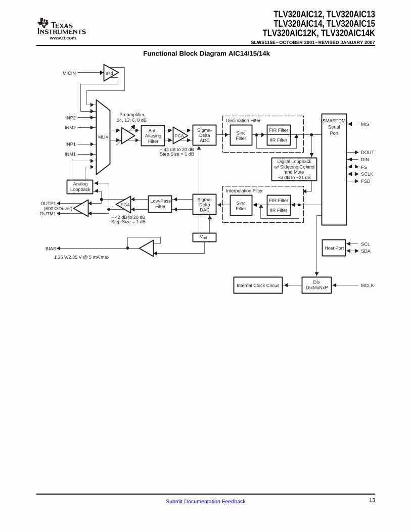
TLV320AIC12, TLV320AIC13TLV320AIC14, TLV320AIC15TLV320AIC12K, TLV320AIC14KSLWS115E–OCTOBER 2001–REVISED JANUARY 2007
Functional Block Diagram AIC12/13/12k
12 Submit Documentation Feedback
www.ti.com
MUX
AnalogLoopback
(600 ΩDriver)
MICIN
INP2
INM2
INP1
INM1
OUTP1
OUTM1
BIAS
PGA
− 42 dB to 20 dBStep Size = 1 dB
Low-PassFilter
Sigma-DeltaDAC
Anti-Aliasing
Filter
Sigma-DeltaADC
SincFilter
FIR Filter
IIR Filter
Decimation Filter
SincFilter
FIR Filter
IIR Filter
Interpolation Filter
Digital Loopbackw/ Sidetone Control
and Mute
M/S
DOUT
DIN
FS
SCLK
FSD
SCL
SDAHost Port
Div16xMxNxPInternal Clock Circuit MCLK
PGA
− 42 dB to 20 dBStep Size = 1 dB
SMARTDMPreamplifier
24, 12, 6, 0 dB
−3 dB to −21 dB
1.35 V/2.35 V @ 5 mA max
SerialPort
Vref
s2d
TLV320AIC12, TLV320AIC13TLV320AIC14, TLV320AIC15
TLV320AIC12K, TLV320AIC14KSLWS115E–OCTOBER 2001–REVISED JANUARY 2007
Functional Block Diagram AIC14/15/14k
13Submit Documentation Feedback

www.ti.com
Definitions and Terminology
TLV320AIC12, TLV320AIC13TLV320AIC14, TLV320AIC15TLV320AIC12K, TLV320AIC14KSLWS115E–OCTOBER 2001–REVISED JANUARY 2007
Term Definition
Data Transfer The time during which data is transferred from DOUT and to DIN. The intervalInterval is 16 shift clocks and the data transfer is initiated by the falling edge of the FS
signal in standard and continuous mode.
Signal Data This refers to the input signal and all of the converted representations throughthe ADC channel and the signal through the DAC channel to the analog output.This is contrasted with the purely digital software control data.
Frame Sync Frame sync refers only to the falling edge of the signal FS that initiates the datatransfer interval
Frame Sync and Sampling Frame sync and sampling period is the time between falling edges ofPeriod successive FS signals.
fs The sampling frequency
ADC Channel ADC channel refers to all signal processing circuits between the analog inputand the digital conversion result at DOUT.
DAC channel DAC channel refers to all signal processing circuits between the digital dataword applied to DIN and the differential output analog signal available at OUTPand OUTM.
Dxx Bit position in the primary data word (xx is the bit number)
DSxx Bit position in the secondary data word (xx is the bit number)
PGA Programmable gain amplifier
IIR Infinite impulse response
FIR Finite impulse response
14 Submit Documentation Feedback

www.ti.com
Timing Requirements
th1
2.4 VMCLK
RESET
2.4 V
tsu1
2.4 V
twL
twH
td1td2 td1
td2
tentd3 tdis
tsu2th2
D15
D15
SCLK
FS
FSD
DOUT
DIN
TLV320AIC12, TLV320AIC13TLV320AIC14, TLV320AIC15
TLV320AIC12K, TLV320AIC14KSLWS115E–OCTOBER 2001–REVISED JANUARY 2007
Figure 1. Hardware Reset Timing
Figure 2. Serial Communication Timing
TEST CONDITIONS MIN TYP MAX UNIT
twH Pulse duration, MCLK high 5
twL Pulse duration, MCLK low 5
Setup time, RESET, before MCLK hightsu1 3(see Figure 1)
th1 Hold time, RESET, after MCLK high (see Figure 1) 2
td1 Delay time, SCLK↑ to FS/FSD↓ CL = 20 pF 5 ns
td2 Delay time, SCLK↑ to FS/FSD↑ 5
td3 Delay time, SCLK↑ to DOUT 15
ten Enable time, SCLK↑ to DOUT 15
tdis Disable time, SCLK↑ to DOUT 15
tsu2 Setup time, DIN, before SCLK↓ 10
th2 Hold time, DIN, after SCLK↓ 10
15Submit Documentation Feedback

www.ti.com
SDA
SCL
tSU;STO
tBUFtrtHD;STA
tSU;STAtHIGHtHD;DAT
tHD;STA
tLOWtftr tf
tSU;OAT
Parameter Measurement Information
-160
-140
-120
-100
-80
-60
-40
-20
0
0 1000 2000 3000
Am
pli
tud
e -
dB
f - Frequency - Hz
500 1500 2500 3500 4000
Sampling Rate at 8 kHz
TLV320AIC12, TLV320AIC13TLV320AIC14, TLV320AIC15TLV320AIC12K, TLV320AIC14KSLWS115E–OCTOBER 2001–REVISED JANUARY 2007
Figure 3. I2C / S2C Timing
TEST CONDITIONS MIN MAX UNIT
tSCL SCL clock frequency 0 900 kHz
tHD;STA Hold time (repeated START condition. After this 100 nsperiod, the first clock pulse is generated.
tLOW Low period of the SCL clock 560 ns
tHIGH High period of the SCL clock 560 ns
tSU;STA Set-up time for a repeated START condition CL = 20 pF 100 ns
tHD;DAT Data hold time 50 ns
tSU;DAT Data set-up time 50 ns
tr Rise time of both SDA and SCL signals 300 ns
tf Fall time of both SDA and SCL signals 100 ns
tSU;STO Set-up time for STOP condition 100 ns
tBUF Bus free time between a STOP and START condition 500 ns
Figure 4. FFT—ADC Channel (-1 dB Input)
16 Submit Documentation Feedback

www.ti.com
-160
-140
-120
-100
-80
-60
-40
-20
0
0 1000 2000 3000
Am
pli
tud
e -
dB
f - Frequency - Hz
500 1500 2500 3500 4000
Sampling Rate at 8 kHz
-160
-140
-120
-100
-80
-60
-40
-20
0
0 1000 2000 3000
Am
pli
tud
e -
dB
f - Frequency - Hz
500 1500 2500 3500 4000
Sampling Rate at 8 kHz
-160
-140
-120
-100
-80
-60
-40
-20
0
0 1000 2000 3000
Am
pli
tud
e -
dB
f - Frequency - Hz
500 1500 2500 3500 4000
Sampling Rate at 8 kHz
TLV320AIC12, TLV320AIC13TLV320AIC14, TLV320AIC15
TLV320AIC12K, TLV320AIC14KSLWS115E–OCTOBER 2001–REVISED JANUARY 2007
Parameter Measurement Information (continued)
Figure 5. FFT—ADC Channel (-9 dB Input)
Figure 6. FFT—DAC Channel (0 dB Input)
Figure 7. FFT—DAC Channel (-9 dB Input)
17Submit Documentation Feedback

www.ti.com
-140
-120
-100
-80
-60
-40
-20
0
0 4000 8000 12000
Am
pli
tud
e -
dB
f - Frequency - Hz
2000 6000 10000 14000 16000
ADC at 8 kHzFs = 32 kHz
-140
-120
-100
-80
-60
-40
-20
0
0 4000 8000 12000
Am
pli
tud
e -
dB
f - Frequency - Hz
2000 6000 10000 14000 16000
DAC at 8 kHzFs = 32 kHz
TLV320AIC12, TLV320AIC13TLV320AIC14, TLV320AIC15TLV320AIC12K, TLV320AIC14KSLWS115E–OCTOBER 2001–REVISED JANUARY 2007
Parameter Measurement Information (continued)
Figure 8. FFT—ADC Channel in FIR/IIR Bypass Mode (-1 dB Input)
Figure 9. FFT—DAC Channel in FIR/IIR Bypass Mode (0 dB Input)
18 Submit Documentation Feedback

www.ti.com
TYPICAL CHARACTERISTICS
−30
−25
−20
−15
−10
−5
0
5
0 500 1000 1500 2000 2500 3000 3500 4000
Filt
er G
ain
− dB
f − Frequency − Hz
−40
−35
−30
−25
−20
−15
−10
−5
0
5
0 500 1000 1500 2000 2500 3000 3500 4000F
ilter
Gai
n −
dB
f − Frequency − Hz
−45
0
3
4
5
6
7
8
9
0 500 1000 1500 2000 2500 3000 3500 4000
Gro
up
De
lay
- f
s
f - Frequency - Hz
1
2
0
3
4
5
6
7
8
9
0 500 1000 1500 2000 2500 3000 3500 4000
Gro
up
De
lay
- f
s
f - Frequency - Hz
1
2
TLV320AIC12, TLV320AIC13TLV320AIC14, TLV320AIC15
TLV320AIC12K, TLV320AIC14KSLWS115E–OCTOBER 2001–REVISED JANUARY 2007
ADC FILTER GAIN ADC FILTER GAINvs vs
FREQUENCY RESPONSE (FIR) FREQUENCY RESPONSE (IIR)
Figure 10. Figure 11.
ADC IIR FILTER GROUP DELAY DAC IIR FILTER GROUP DELAYvs vs
FREQUENCY FREQUENCY RESPONSE
Figure 12. Figure 13.
19Submit Documentation Feedback
www.ti.com
-14
-8
-6
-4
-2
0
2
4
0 2000 4000 6000 8000 10 k 12 k 14 k 16 k
Fil
ter
Ga
in -
dB
f - Frequency - Hz
-12
-10
-14
-8
-6
-4
-2
0
2
4
0 2000 4000 6000 8000 10 k 12 k 14 k 16 kF
ilte
r G
ain
- d
B
f - Frequency - Hz
-12
-10
−140
−120
−100
−80
−60
−40
−20
0
20
0 1000 2000 3000 4000 5000 6000 7000 8000
Filt
er G
ain
− dB
f − Frequency − Hz
OSR = 512
−120
−100
−80
−60
−40
−20
0
20
0 1000 2000 3000 4000 5000 6000 7000 8000
Filt
er G
ain
− dB
f − Frequency − Hz
OSR = 128
TLV320AIC12, TLV320AIC13TLV320AIC14, TLV320AIC15TLV320AIC12K, TLV320AIC14KSLWS115E–OCTOBER 2001–REVISED JANUARY 2007
TYPICAL CHARACTERISTICS (continued)
ADC FILTER GAIN DAC FILTER GAINvs vs
FREQUENCY (FIR/IIR BYPASS) FREQUENCY (FIR/IIR BYPASS)
Figure 14. Figure 15.
DAC IIR DAC FIRvs vs
FREQUENCY RESPONSE FREQUENCY RESPONSE
Figure 16. Figure 17.
20 Submit Documentation Feedback

www.ti.com
−140
−120
−100
−80
−60
−40
−20
0
20
0 1000 2000 3000 4000 5000 6000 7000 8000
Filt
er G
ain
− dB
f − Frequency − Hz
OSR = 256
−140
−120
−100
−80
−60
−40
−20
0
20
0 1000 2000 3000 4000 5000 6000 7000 8000F
ilter
Gai
n −
dB
f − Frequency − Hz
OSR = 128
Functional Description
Operating Frequencies (see Notes)
TLV320AIC12, TLV320AIC13TLV320AIC14, TLV320AIC15
TLV320AIC12K, TLV320AIC14KSLWS115E–OCTOBER 2001–REVISED JANUARY 2007
TYPICAL CHARACTERISTICS (continued)
DAC FIR DAC FIRvs vs
FREQUENCY RESPONSE FREQUENCY RESPONSE
Figure 18. Figure 19.
The sampling frequency is the frequency of the frame sync (FS) signal whose falling edge starts digital-datatransfer for both ADC and DAC. The sampling frequency is derived from the master clock (MCLK) input by thefollowing equations:• Coarse sampling frequency (default):
– The coarse sampling is selected by programming P = 8 in the control register 4, which is the defaultconfiguration of AIC1x on power-up or reset.
– FS = Sampling (conversion) frequency = MCLK ÷ (16 × M × N × 8)• Fine sampling frequency (see step 5):
– FS = Sampling (conversion) frequency = MCLK ÷ (16 × M × N × P)
NOTES:1. Use control register 4 to set the following values of M, N, and P2. M = 1, 2, . . . , 1283. N = 1, 2,..., 164. P = 1, 2, ..., 85. The fine sampling rate needs an on-chip Phase Lock Loop (frequency multiplier) to generate
internal clocks. The PLL requires the relationship between MCLK and P to meet the followingcondition:10 MHz ≤ (MCLK ÷ P) ≤ 25 MHz. The output of the PLL is only used to generate internal clocksthat are needed by the data converters. Other clocks such as the serial interface clocks in mastermode are not generated from the PLL output. The clock generation scheme is as shown inFigure 20.
21Submit Documentation Feedback

www.ti.com
MCLK1/P
X 8
(DLL)
1/(MN)128 FS
(no_dev x mode) / (MNP)
SCLK
1 / (16 x mode x no_dev)FS
en_dll
M = 1 - 128
N = 1 - 16
P = 1- 8
When P = 8, DLL(PLL) is enabled
devnum = number of devices in cascade
mode = 1 (for continious data tranfer mode)
SCLK may not be an uniform clock depending upon values of devnum, mode, and MNP
Digital
mode = 2 (for programming mode)
*
*
FS 20.48 MHz(16 10 16 1)
8 kHz
Internal Architecture
Analog Low-Pass Filter
Sigma-Delta ADC
TLV320AIC12, TLV320AIC13TLV320AIC14, TLV320AIC15TLV320AIC12K, TLV320AIC14KSLWS115E–OCTOBER 2001–REVISED JANUARY 2007
Functional Description (continued)
Figure 20. AIC1x Clock Tree Architecture
6. Both equation of FS require that the following conditions be met:– (M × N × P) ≥ (devnum × mode) if the FIR/IIR filter is not bypassed.– [Integer (M ÷ 4) × N × P] ≥ (devnum × mode) if the FIR/IIR filter is bypassed.
Where:– devnum is the number of codec channels connecting in cascade mode.– mode is equal to 1 for continuous data transfer mode and 2 for programming mode.
7. If the DAC OSR is set to 512, then M needs to be a multiple of 4. If the DAC OSR is set to 256,then M needs to be a multiple of 2. M can take any value between 1 and 128 if the OSR is set to128.
EXAMPLE:
The MCLK that comes from the DSP 'C5402 CLKOUT equals to 20.48 MHz, and the conversion rateof 8 kHz is desired. First, set P = 1 to satisfy condition step 5 above so that (MCLK ÷ P) = 20.48 MHz÷ 1 = 20.48 MHz. Next, pick M = 10 and N = 16 to satisfy step 6 above and derive 8 kHz for FS.
The built-in analog low-pass filter is a two-pole filter that has a 20-dB attenuation at 1 MHz.
The analog-to-digital converter is a sigma-delta modulator with 128-x oversampling. The ADC provideshigh-resolution, low-noise performance using oversampling techniques. Due to the oversampling employed, onlysingle pole R-C filters are required on the analog inputs.
22 Submit Documentation Feedback

www.ti.com
Decimation Filter
Sigma-Delta DAC
Interpolation Filter
Analog/Digital Loopback
Side-Tone Loopback
ADC PGA
DAC PGA
Analog Input/Output
TLV320AIC12, TLV320AIC13TLV320AIC14, TLV320AIC15
TLV320AIC12K, TLV320AIC14KSLWS115E–OCTOBER 2001–REVISED JANUARY 2007
Functional Description (continued)
The decimation filters are either FIR filters or IIR filters selected by bit D5 of the control register 1. The FIR filterprovides linear-phase output with 17/fs group delay, whereas the IIR filter generates nonlinear phase output withnegligible group delay. The decimation filters reduce the digital data rate to the sampling rate. This isaccomplished by decimating with a ratio of 1:128. The output of the decimation filter is a 16-bit 2s-complementdata word clocking at the sample rate selected. The BW of the filter is (0.45 × FS) and scales linearly with thesample rate.
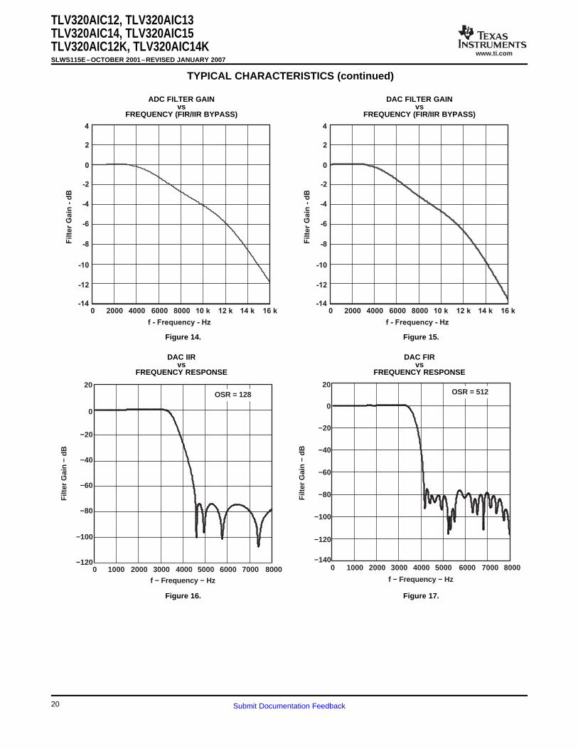
The digital-to-analog converter is a sigma-delta modulator with 128/256/512-x oversampling. The DAC provideshigh-resolution, low-noise performance using oversampling techniques. The oversampling ratio in DAC isprogrammable to 256/512 using bits D4-D3 of control register 3, the default being 128. Oversampling ratio of512 can be used when FS is a maximum of 8 Ksps and an oversampling ratio of 256 can be used when FS is amaximum of a 16 Ksps. M should be a multiple of 2 for an oversampling ratio of 256 and 4 for oversamplingratio of 512.
The interpolation filters are either FIR filters or IIR filters selected by bit D5 of the control register 1. The FIR filterprovides linear-phase output with 18/fs group delay, whereas the IIR filter generates nonlinear phase output withnegligible group delay. The interpolation filter resamples the digital data at a rate of 128/256/512 times theincoming sample rate, based on the oversampling rate of DAC. The high-speed data output from theinterpolation filter is then used in the sigma-delta DAC. The BW of the filter is (0.45 × FS) and scales linearlywith the sample rate.
The analog and digital loopbacks provide a means of testing the data ADC/DAC channels and can be used forin-circuit system level tests. The analog loopback always has the priority to route the DAC low pass filter outputinto the analog input where it is then converted by the ADC to a digital word. The digital loopback routes theADC output to the DAC input on the device. Analog loopback is enabled by writing a 1 to bit D2 in the controlregister 1. Digital loopback is enabled by writing a 1 to bit D1 in control register 1.
The side-tone digital loopback attenuates the ADC output and mixes it with the input of the DAC. The level of theside tone is set by DSTG, bits D5-D3 of the control register 5C.
TLV320AIC1x has a built-in PGA for controlling the signal levels at ADC outputs. ADC PGA gain setting can beselected by writing into bits D5-D0 of register 5A. The PGA range of the ADC channel is 20 dB to -42 dB insteps of 1 dB and mute. To avoid sudden jumps in signal levels with PGA changes, the gains are appliedinternally with zero-crossovers.
TLV320AIC1x has a built-in PGA for controlling the analog output signal levels in DAC channel. DAC PGA gainsetting can selected by writing into bits D5-D0 of register 5B. The PGA range of the DAC channel is 20 dB to -42dB in steps of 1 dB, and mute. To avoid sudden pop-sounds with power-up/down and gain changes thepower-up/down and gain changes for DAC channel are applied internally with zero-crossovers.
The TLV320AIC1x has three programmable analog inputs and three programmable analog outputs. Bits D2-D1of control register 6 select the analog input source from MICIN, INP1/M1, or INP2/M2. All analog I/O are eithersingle-ended or differential. All analog input signals are self-biased to 1.35 V. The three analog outputs areconfigured by bits D7, D6, D5, and D4-D3 of control register 6.
23Submit Documentation Feedback

www.ti.com
MIC Input
TLV320AIC12 TLV320AIC12
BIAS
MICIN
10 kΩ
0.1 µF
ElectretMicrophone
BIAS
MICIN
INM1
0.1 µF
10 kΩ
0.1 µF
ElectretMicrophone
(a) Single Ended (b) Pseudo -Differential (High Quality)
INP and INM Input
INP1 or INP2
INM1 or INM2
1.35 V
TLV320AIC12
V(INP)
V(INM)
Single-Ended Analog Input
TLV320AIC12, TLV320AIC13TLV320AIC14, TLV320AIC15TLV320AIC12K, TLV320AIC14KSLWS115E–OCTOBER 2001–REVISED JANUARY 2007
Functional Description (continued)
TLV320AIC1x supports single ended microphone input. This can be used by connecting the external singleended source through ac coupling to the MICIN pin. This channel is selected by writing 01 or 10 into bits D2-D1in control register 6. The single ended input is supported in two modes.
Writing 01 into bits D2-D1 chooses self biased MICIN mode. In this mode, the device internally self-biases theinput at 1.35V. For best noise performance, the user should bias the microphone circuit using the BIAS voltagegenerated by the device as shown in Figure 21.
Writing 10 into bits D2-D1 chooses pseudo-differential MICIN mode. In this mode, the single ended input isconnected through ac-coupling to MICIN and the bias voltage used to generate the signal is also ac coupled toINM1 as shown in Figure 22. For best noise performance, the MICIN and INM1 lines must be routed in similarfashion from the microphone to the device for noise cancellation.
For high quality performance, the single ended signal is converted internally into differential signal before beingconverted. To improve the dynamic range with different types of microphones, the device supports a preamplifierwith gain settings of 0/6/12/24 dB. This can be chosen by writing into bits D1-D0 of control register 5C.
Figure 21. Microphone Interface
To produce common-mode rejection of unwanted signal performance, the analog signal is processeddifferentially until it is converted to digital data. The signal applied to the terminals INM1/2 and INP1/2 aredifferential to preserve device specifications (see Figure 22). The signal source driving analog inputs (INP1/2and INM1/2) should have low source impedance for lowest noise performance and accuracy. To obtainmaximum dynamic range, the signal should be ac-coupled to the input terminal.
Figure 22. INP and INM Internal Self-Biased Circuit
The two differential inputs of (INP1/M1 and INP2/M2) can be configured to work as single-ended inputs byconnecting INP to the analog input and INM to ground (see Figure 23).
24 Submit Documentation Feedback

www.ti.com
INP1 or INP2
INM1 or INM2
C
C
Analog Input
Analog Output
OUTP1
OUTM1
RL
Differential Output OUTP/OUTM
OUTP1
OUTM1
RL
Single-Ended Output OUTP/OUTM
C
OUTP2
OUTP3
RL
OUTMV
RL
TLV320AIC12, TLV320AIC13TLV320AIC14, TLV320AIC15
TLV320AIC12K, TLV320AIC14KSLWS115E–OCTOBER 2001–REVISED JANUARY 2007
Functional Description (continued)
Figure 23. Single-Ended Input
The OUTP and OUTM are differential output from the DAC channel. The OUTP1 and OUTM1 can drive a loadof 600-Ω directly and be either differential or single-ended (see Figure 24). The OUTP2 and OUTP3 are outputfrom two audio amplifiers to drive low-voltage speakers like those in the handset and headset. They can drive aload of 16-Ω directly and be configured as either differential output or single-ended output as by bit D7 of thecontrol register 6 (see Figure 25). If OUTP2 and OUTP3 are differential output, the OUTMV pin becomes thecommon inverting output. Both OUTP2 and OUTP3 can be used simultaneously if each differential load RL >32Ω . This is because OUTMV amplifier can drive a maximum load of 16 Ω only (only one driver used) or aparallel combination of two 32-Ω loads (both drivers used). If both OUTP2 and OUTP3 are used simultaneously,they are muted at the same time if MUTE is selected.
Otherwise, the OUTMV pin is configured as the virtual ground for single-ended output and equal to the commonmode voltage at 1.35 V.
Figure 24. OUTP1/OUTM1 Output
Figure 25. Single-Ended/Differential Connection of OUTP2/OUTP3 Output
Analog Output Configuration
SPEAKER DRIVER CONFIGURATION NO. OF SPEAKER DRIVERS ON MIN LOAD
Single-ended 1 16-Ω
Single-ended 2 32-Ω
Differential 1 16-Ω
25Submit Documentation Feedback

www.ti.com
IIR/FIR Control
Overflow Flags
IIR/FIR Bypass Mode
System Reset and Power Management
Software and Hardware Reset
TLV320AIC12, TLV320AIC13TLV320AIC14, TLV320AIC15TLV320AIC12K, TLV320AIC14KSLWS115E–OCTOBER 2001–REVISED JANUARY 2007
Functional Description (continued)
Analog Output Configuration (continued)
SPEAKER DRIVER CONFIGURATION NO. OF SPEAKER DRIVERS ON MIN LOAD
Differential 2 32-Ω
The decimation IIR/FIR filter sets an overflow flag (bit D7) of control register 1 indicating that the input analogsignal has exceeded the range of internal decimation filter calculations. The interpolation IIR/FIR filter sets anoverflow flag (bit D4) of control register 1 indicating that the digital input has exceeded the range of internalinterpolation filter calculations. When the IIR/FIR overflow flag is set in the register, it remains set until the userreads the register. Reading this value resets the overflow flag. These flags need to be reset after power-up byreading the register. If FIR/IIR overflow occurs, the input signal is attenuated by either the PGA or some othermethod.
An option is provided to bypass IIR/FIR filter sections of the decimation filter and the interpolation filter. Thismode is selected through bit D6 of control register 2 and effectively increases the frequency of the FS signal tofour times normal output rate of the IIR/FIR-filter. For example, for a normal sampling rate of 8 Ksps (i.e., FS =8 kHz) with IIR/FIR, if the IIR/FIR is bypassed, the frequency of FS is readjusted to 4×8 kHz = 32 kHz. The sincfilters of the two paths can not be bypassed. A maximum of eight devices in cascade can be supported in theIIR/FIR bypassed mode.
In this mode , the ADC channel outputs data which has been decimated only until 4Fs. Similarly DAC channelinput needs to be preinterpolated to 4Fs before being given to the device. This mode allows users the flexibilityto implement their own filter in DSP for decimation and interpolation. M should be a multiple of 4 during IIR/FIRBypass mode. The frequency responses of the IIR/FIR bypass modes are shown in Figure 14 and Figure 15.
The TLV320AIC1x resets internal counters and registers in response to either of two events:• A low-going reset pulse is applied to terminal RESET• A 1 is written to the programmable software reset bits (D5 of control register 3)
• NOTE: The TLV320AIC1x requires a power-up reset applied to the RESET pin before normal operation isstarted.
Either event resets the control registers and clears all sequential circuits in the device. The H/W RESET (activelow) signal is at least 6 master clock periods long. As soon as the RESET input is applied, the TLV320AIC1xenters the initialization cycle that lasts for 132 MCLKs, during which the serial port of the DSP must be tristated.The initialization sequence performed by the 'AIC1x is known as auto cascade detection (ACD). ACD is amechanism that allows a device to know its address in a cascade chain. Up to 16 'AIC1x devices can becascaded together. The master device is the first device on the chain (i.e. the FS of the master is connected tothe FS of the DSP). During ACD, each device gets to know the number of devices in the chain as well as itsrelative position in the chain. This is done on hardware reset. Therefore, after power up, a hardware reset mustbe done. ACD requires 132 MCLKs after reset to complete operation. The number of MCLKs is independent ofthe number of devices in the chain. Adjacent devices in the chain have their FS and FSD pins connected toeach other. The master device FS is connected to the FS pin of the DSP. The FSD pin on the last device in thechain is pulled high. The master device has the highest address (i.e. 0, the next device in the chain has anaddress of 1, followed by 2 etc.).
During the first 64 MCLKs, FS is configured as an output and FSD as an input. During the next 64 MCLKs, FS isconfigured as an input and FSD as an output. The master device always has FS configured as an output andthe last slave in the cascade (i.e. channel with address 0) always has FSD configured as an input.
26 Submit Documentation Feedback

www.ti.com
Power Management
Software Power-Down
Hardware Power-Down
Host Port Interface
TLV320AIC12, TLV320AIC13TLV320AIC14, TLV320AIC15
TLV320AIC12K, TLV320AIC14KSLWS115E–OCTOBER 2001–REVISED JANUARY 2007
To calculate the channel address, during the first 64 MCLKs, the device counts the number of clocks betweenACD starting (reset) and the FSD going high. During the next 64 MCLKs, the device counts the number ofclocks till FS is pulled low. The sum total of the counts in the first phase and the second phase is the number ofdevices in the channel.
For a cascaded system, the rise time of H/W RESET needs to be less than the MCLK period and should satisfysetup time requirement of 2 ns with respect to MCLK rise-edge. In stand-alone-slave mode SCLK must berunning during RESET. If more than one codec is cascaded, RESET must be synchronized to MCLK.Additionally, all devices must see the same edge of MCLK within a window of 0.5 ns The reset signal need notbe synchronized with MCLK when the codec is in stand-alone master or slave configuration.
Most of the device (all except the digital interface) enters the power-down mode when D7 and D6, in controlregister 3, are set to 1. When the PWRDN pin is low, the entire device is powered down. In either case, registercontents are preserved.
The amount of power drawn during software power down is higher than during a hardware power down becauseof the current required to keep the digital interface active. Additional differences between software and hardwarepower-down modes are detailed in the following paragraphs.
Data bits D7 and D6 of control register 3 are used by TLV320AIC1x to turn on or off the software power-downmode, which takes effect in the next frame FS. The ADC and DAC can be powered down individually. In thesoftware power-down, the digital interface circuit is still active while the internal ADC and DAC channel anddifferential outputs OUTPx and OUTMx are disabled, and DOUT is put in 3-state in the data frame only. Registerdata in the control frame is still accepted via DIN, but data in the data frame is ignored. The device returns tonormal operation when D7 and D6 of control register 3 are reset.
The TLV320AIC1x requires the PWRDN signal to be synchronized with MCLK. When PWRDN is held low, thedevice enters hardware power-down mode. In this state, the internal clock control circuit and the differentialoutputs are disabled. All other digital I/Os are disabled and DIN cannot accept any data input. The device canonly be returned to normal operation by holding PWRDN high. Getting out of the power-down mode (i.e. bringingPWRDN from low to high state) requires that the low-to-high transition of PWRDN be synchronous to the risingedge of MCLK. If there is no need for the hardware power-down mode feature of the device, the PWRDN pinmust be tied high.
The host port uses a 2-wire serial interface (SCL, SDA) to program the AIC1x's six control registers andselectable protocol between S2C mode and I2C mode. The S2C is a write-only mode and the I2C is a read-writemode selected by setting the bits D1 and D0 of control register 2 to 00 or 01. If the host interface is not neededthe two pins of SCL and SDA can be programmed to become general-purpose I/Os by setting the bits D1 andD0 of control register 2 to 10 or 11. If selected to be used as I/O pins, the SDA and SCL pins become outputand input pins respectively, determined by D1 and D0.
Both S2C and I2C require a SMARTDM device address to communicate with the AIC1x. One of SMARTDMsadvanced features is the automatic cascade detection (ACD) that enables SMARTDM to automatically detectthe total number of codecs in the serial connection and use this information to assign each codec a distinctSMARTDM device address. Table 1 lists device addresses assigned to each codec in the cascade by theSMARTDM. The master always has the highest position in the cascade. For example, if there is a total of 8codecs in the cascade (i.e., one master and 7 slaves), then the device addresses in row 8 are used in which themaster is codec 7 with a device address of 0111.
Table 1. SMARTDM Device Addresses
TOTAL CODEC POSITION IN CASCADECODECS 15 14 13 12 11 10 9 8 7 6 5 4 3 2 1 0
1 0000
27Submit Documentation Feedback

www.ti.com
S2C (Start-Stop Communication)
D15 D14 D13 D12 D11 D10 D9 D8 D7 D6 D5 D4 D3 D2 D1 D0
SCL
SDA
Start Bit = 0 Stop Bit = 1SMARTDM Device
Address(see Table 1)
RegisterAddress
Register Content
I2C
TLV320AIC12, TLV320AIC13TLV320AIC14, TLV320AIC15TLV320AIC12K, TLV320AIC14KSLWS115E–OCTOBER 2001–REVISED JANUARY 2007
Table 1. SMARTDM Device Addresses (continued)
TOTAL CODEC POSITION IN CASCADECODECS 15 14 13 12 11 10 9 8 7 6 5 4 3 2 1 0
2 0001 0000
3 0010 0001 0000
4 0011 0010 0001 0000
5 0100 0011 0010 0001 0000
6 0101 0100 0011 0010 0001 0000
7 0110 0101 0100 0011 0010 0001 0000
8 0111 0110 0101 0100 0011 0010 0001 0000
9 1000 0111 0110 0101 0100 0011 0010 0001 0000
10 1001 1000 0111 0110 0101 0100 0011 0010 0001 0000
11 1010 1001 1000 0111 0110 0101 0100 0011 0010 0001 0000
12 1011 1010 1001 1000 0111 0110 0101 0100 0011 0010 0001 0000
13 1100 1011 1010 1001 1000 0111 0110 0101 0100 0011 0010 0001 0000
14 1101 1100 1011 1010 1001 1000 0111 0110 0101 0100 0011 0010 0001 0000
15 1110 1101 1100 1011 1010 1001 1000 0111 0110 0101 0100 0011 0010 0001 0000
16 1111 1110 1101 1100 1011 1010 1001 1000 0111 0110 0101 0100 0011 0010 0001 0000
The S2C is a write-only interface selected by programming bits D1-D0 of control register 2 to 01. The SDA inputis normally in a high state, pulled low (START bit) to start the communication, and pulled high (STOP bit) afterthe transmission of the LSB. SCLK and FS must be active during register programming. Figure 26 shows thetiming diagram of S2C. The S2C also supports a broadcast mode in which the same register of all devices incascade is programmed in a single write. To use S2Cs broadcast mode, execute the following steps:
1. Write 111 1000 1111 1111 after the start bit to enable the broadcast mode.2. Write data to program control register as specified in Figure 26 with bits D14-D11 = XXXX (don't care).3. Write 111 1000 0000 0000 after the start bit to disable the broadcast mode.
Figure 26. S2C Programming
• Each I2C read-from or write-to 'AIC1xs control register is given by index register address.• Read/write sequence always starts with the first byte as I2C address followed by 0. During the second byte,
default/broadcast mode is set and the index register address is initialized. For write operation control register,data to be written is given from the third byte onwards. For read operation, stop-start is performed after thesecond byte. Now the first byte is I2C address followed by 1. From the second byte onwards, control registerdata appears.
• Each time read/write is performed, the index register address is incremented so that next read/write isperformed on the next control register.
• During the first write cycle and all write cycles in the broadcast, only the device with address 0000 issuesACK to the I2C.
28 Submit Documentation Feedback

www.ti.com
I2C Write Sequence
SCL
SDAA5 A4 A3 A2 A1 A0 0 ACK B7 B6 B5 B4 B3 R2 R1 R0
I2C
6
A6
I2C
5
I2C
4
D7 D6 D5 D4 D3 D2 D1 D0 D7 D6 D5 D4 D3 D2 D1 D0ACK ACK ACK
Programmable I C Device Address2Set by Control Register 2
Start Bit = 0 SMARTDM Device
Address
(see Table 1)
00000 = Default
11111 = Broadcast Mode
Index Register Address
(Index) Control Register Data for Write
(Index)
Control Register Data for Write
(Index+1)
SCL
SDA A5 A4 A3 A2 A1 A0 0 ACK B7 B6 B5 B4 B3 R2 R1 R0
I2C
6
A6 ACK
I2C
5
I2C
4
SCL
SDA A5 A4 A3 A2 A1 A0 1 ACK D7 D6 D5 D4 D3 D2 D1 D0
I2C6
A6
I2C5
I2C4
D7 D6 D5 D4 D3 D2 D1 D0ACK ACK
Start Bit = 0
Programmable 12C Device Address
Set by Control Register 2
SMARTDM Device Address
(see Table 1)
Index Register Address
(Index)
Stop Bit = 1xxxxx = Don't Care
Start Bit = 0
Programmable 12C Device Address
Set by Control Register 2
SMARTDM Device Address
(see Table 1)
Control Register Data
(Index)
Control Register Data
(Index+1)
I2C Read Sequence
TLV320AIC12, TLV320AIC13TLV320AIC14, TLV320AIC15
TLV320AIC12K, TLV320AIC14KSLWS115E–OCTOBER 2001–REVISED JANUARY 2007
Figure 27. I2C Write Sequence
Figure 28. I2C Read Sequence
Each AIC has an index register address. To perform a write operation, make the LSB of the first byte as 0 (write)(see Figure 29). During the second byte, the index register address is initialized and mode (broadcast/default) isset. From the third byte onwards, write data to the control register (given by index register) and increment theindex register until stop or repeated start occurs. For operation, make the LSB of the first byte as 1 (read). Fromthe second byte onwards, AIC starts transmitting data from the control register (given by the index register) andincrements the index register. For setting the index register perform operation the same as write case for 2bytes, and then give a stop or repeated start.• S/Sr -> Start/Repeated Start.
29Submit Documentation Feedback

www.ti.com
S/Sr I2C Device Address (3 Bit)+
Dtdmsp Device Address (+)
R/W
= 0
Mode (5 Bit) + Index RegAddress
(3 Bit)
Ack Ack Control Reg. Data(Write)
Ack Control Reg. Data(Write)
7 Bit 1 Bit 8 Bit 8 Bit 8 Bit
Increment Index Reg. AddressDefault/Broadcast(00000/11111)
Write Mode
To the Address Givenby Index Reg. Address
To the Address Givenby Index Reg. Address
S/Sr I2C Device Address (3 Bit)+
Dtdmsp Device Address (+)
R/W
= 1
Control Reg. Data(Read)
Ack Ack Control Reg. Data(Read)
Ack
7 Bit 1 Bit 8 Bit 8 Bit
Read Mode
From the Address Givenby Index Reg. Address
From the Address Givenby Index Reg. Address
Increment Index Reg. AddressIncrement Index Reg. Address
S/Sr I2C Device Address (3 Bit)+
Dtdmsp Device Address (+)
R/W
= 0
Mode (5 Bit) + Index Reg.Address
(3 Bit)Ack Ack
7 Bit 1 Bit 8 Bit
For Initializing Index Reg AddressStop
Smart Time Division Multiplexed Serial Port (SMARTDM)
TLV320AIC12, TLV320AIC13TLV320AIC14, TLV320AIC15TLV320AIC12K, TLV320AIC14KSLWS115E–OCTOBER 2001–REVISED JANUARY 2007
Figure 29. Index Register Addresses
The Smart time division multiplexed serial port (SMARTDM) uses the 4 wires of DOUT, DIN, SCLK, and FS totransfer data into and out of the AIC1x. The TLV320AIC1x's SMARTDM supports three serial interfaceconfigurations (see Table 2): stand-alone master, stand-alone slave, and master-slave cascade, employing atime division multiplexed (TDM) scheme (a cascade of only-slaves is not supported). The SMARTDM allows fora serial connection of up to 16 codecs to a single serial port. Data communication in the three serial interfaceconfigurations can be carried out in either standard operation (Default) or turbo operation. Each operation hastwo modes; programming mode (default mode) and continuous data transfer mode. To switch from theprogramming mode to the continuous data transfer mode, set bit D6 of control register 1 to 1, which is resetautomatically after switching back to programming mode. The TLV320AIC1x can be switched back from thecontinuous data transfer mode to the programming mode by setting the LSB of the data on DIN to 1, only if thedata format is (15+1), as selected by bit 0 of control register 1. The SMARTDM automatically adjusts the numberof time slots per frame sync (FS) to match the number of codecs in the serial interface so that no time slot iswasted. Both the programming mode and the continuous data transfer mode of the TLV320AIC1x arecompatible with the TLV320AIC10. The TLV320AIC1x provides primary/secondary communication andcontinuous data transfer with improvements and eliminates the requirements for hardware and software requestsfor secondary communication as seen in other devices. The TLV320AIC1x continuous data transfer mode nowsupports both master/slave stand alone and cascade.
Table 2. Serial Interface Configurations
M/S PIN FSD PINTLV320AIC1x CONNECTIONS COMMENTS
MASTER SLAVE MASTER SLAVE
Stand-alone master High NA Pull high NA
Stand-alone slave NA Low NA Pull-low
Connect to the next slave's FSMaster-slave cascade High Low Last slave's FSD pin is pulled high(see Figure 32)
Slave-slave cascade NA NA NA NA Not supported
30 Submit Documentation Feedback

www.ti.com
Digital Interface
SCLK
FS
DIN/DOUT(16 Bit)
MSB LSB
D15 D14 D1 D0
0 1 15 1614
D15
16 SCLKs
TLV320AIC12, TLV320AIC13TLV320AIC14, TLV320AIC15
TLV320AIC12K, TLV320AIC14KSLWS115E–OCTOBER 2001–REVISED JANUARY 2007
Clock Source (MCLK, SCLK)
MCLK is the external master clock input. The clock circuit generates and distributes necessary clocks throughoutthe device. SCLK is the bit clock used to receive and transmit data synchronously. When the device is in themaster mode, SCLK and FS are output and derived from MCLK in order to provide clocking the serialcommunications between the device and a digital signal processor (DSP). When in the slave mode, SCLK andFS are inputs. In the non-turbo mode (TURBO = 0), SCLK frequency is defined by:• SCLK = (16 × FS × #Devices × mode)
Where:• FS is the frame-sync frequency. #Device is the number of the device in cascade. Mode is equal to 1 for
continuous data transfer mode and 2 for programming mode.
In turbo mode, see the Turbo Mode Operation section of this data sheet.
Serial Data Out (DOUT)
DOUT is placed in the high-impedance state after transmission of the LSB is completed. In data frame, the dataword is the ADC conversion result. In the control frame, the data is the register read results when requested bythe read/write (R/W) bit. If a register read is not requested, the low eight bits of the secondary word are allzeroes. Valid data on DOUT is taken from the high-impedance state by the falling edge of frame-sync (FS). Thefirst bit transmitted on the falling edge of FS is the MSB of valid data.
Serial Data In (DIN)
The data format of DIN is the same as that of DOUT, in which MSB is received first on the falling edge of FS. Ina data frame, the data word is the input digital signal to the DAC channel. If (15+1)-bit data format is used, theLSB (D0) is set to 1 to switch from the continuous data transfer mode to the programming mode. In a controlframe, the data is the control and configuration data that sets the device for a particular function as described inthe Control Register Programming section.
Frame-Sync FS
The frame-sync signal (FS) indicates the device is ready to send and receive data. The FS is an output if theM/S pin is connected to HI (master mode), and an input if the M/S pin is connected to LO (slave mode).
The start of valid data is synchronized on the falling edge of the FS signal. In nonturbo mode, the FS signalmust be present every (16 SCLK × mode). However, in turbo mode, the number of SCLK per FS cycle can vary.
The frequency of FS is defined as the sampling rate of the TLV320AIC1x and derived from the master clock,MCLK, as follows (see Operating Frequencies section for details):• FS = MCLK ÷ (16 × P × N × M)
Figure 30. Timing Diagram of FS
Cascade Mode and Frame-Sync Delayed (FSD)
In cascade mode, the DSP should be in slave mode, it receives all frame-sync pulses from the master though
31Submit Documentation Feedback

www.ti.com
TLV320AIC12, TLV320AIC13TLV320AIC14, TLV320AIC15TLV320AIC12K, TLV320AIC14KSLWS115E–OCTOBER 2001–REVISED JANUARY 2007
the master's FS. The master FSD is output to the first slave and the first slave's FSD is output to the secondslave device and so on. When the codecs are configured in cascade mode, MCLK must be connected in starconfiguration to ensure that MCLK can propagate simultaneously to all the codecs in the chain in less then 2 ps.Figure 32 shows the cascade of 4 TLV320AIC1xs in which the closest one to DSP is the master and the rest areslaves. The FSD output of each device is input to the FS terminal of the succeeding device. Figure 30 shows theFSD timing sequence in the cascade.
Stand-Alone Slave
In the stand-alone slave connection, the FS and SCLK are input in which they need to be synchronized to eachother and programmed according to the Operating Frequencies section of this data sheet. The FS and SCLKinput are not required to synchronize to the MCLK input but must remain active at all times to assure continuoussampling in the data converter. FS is output for initial 132 MCLK and it is kept low. DSP needs to keep FS low orhigh-impedance state for this period to avoid contention on FS.
In addition, SCLK must be running at all times when the device is put into reset when in slave mode.
32 Submit Documentation Feedback

www.ti.com
SCLK
FSD(Output)
DIN/DOUT(16 Bit)
MSB LSB
D15 D14 D2 D1
0 1 14 1513
D0
FS
16 SCLKs
MCLK
DIN
DOUT
FS
SCLK
MCLK
DIN
DOUT
FS
SCLK
MCLK
DIN
DOUT
FS
SCLK
Slave 2 Slave 1 Slave 0Master
MCLK
DIN
DOUT
FSD
SCLK
FSD FSD
FS
CLKOUTDXDR
FSX
FSR
CLKX
CLKR
TMS320C5x
M/S M/S M/S M/S
FSD
IOVDD
1 kΩ
100 MHz Max
IOVDD
TLV320AIC12, TLV320AIC13TLV320AIC14, TLV320AIC15
TLV320AIC12K, TLV320AIC14KSLWS115E–OCTOBER 2001–REVISED JANUARY 2007
Asynchronous Sampling (Codecs in cascade are sampled at different sampling frequency)
The 'AIC1x SMARTDM supports a different sampling frequency between the codecs in cascade connecting to asingle serial port. All codecs are required to have a common frame synch frequency. The FS signal is calculatedusing step 1. The desired sampling frequencies of the individual codecs are then calculated using bits D2-D0 ofcontrol register 3 as shown in step 2 and step 3.
1. FS = MCLK ÷ (16 × M × N × P)2. FS = n1 × fs1 (n1 = 1,2, 8 defined in the control register 3 of CODEC1)3. FS = n2 × fs2 (n2 = 1,2, 8 defined in the control register 3 of CODEC2)
The DSP should transfer data at the common FS rate used by the serial interface. The task of decimating andinterpolating the data suitably for each codec is left to the DSP.
Figure 31. Timing Diagram for FSD Output
Figure 32. Cascade Connection (To DSP Interface)
33Submit Documentation Feedback
www.ti.com
Master Slave2 Slave1 Slave0 Slave2Master
Master FS
DIN/DOUT
Master FSD,Slave 2 FS
Slave 2 FSD,Slave 1 FS
Slave 1 FSD,Slave 0 FS
Slave 0 FSD,(see Note)
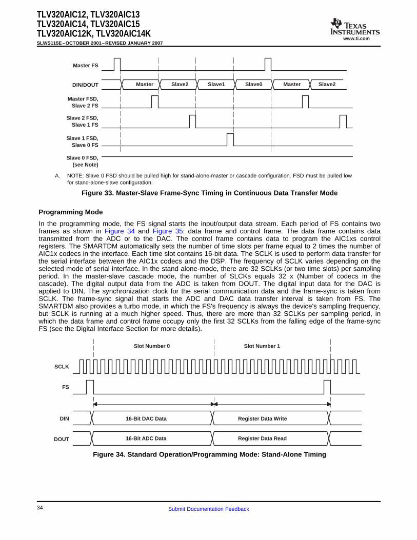
Programming Mode
SCLK
FS
DIN
DOUT
16-Bit DAC Data Register Data Write
16-Bit ADC Data Register Data Read
Slot Number 0 Slot Number 1
TLV320AIC12, TLV320AIC13TLV320AIC14, TLV320AIC15TLV320AIC12K, TLV320AIC14KSLWS115E–OCTOBER 2001–REVISED JANUARY 2007
A. NOTE: Slave 0 FSD should be pulled high for stand-alone-master or cascade configuration. FSD must be pulled lowfor stand-alone-slave configuration.
Figure 33. Master-Slave Frame-Sync Timing in Continuous Data Transfer Mode
In the programming mode, the FS signal starts the input/output data stream. Each period of FS contains twoframes as shown in Figure 34 and Figure 35: data frame and control frame. The data frame contains datatransmitted from the ADC or to the DAC. The control frame contains data to program the AIC1xs controlregisters. The SMARTDM automatically sets the number of time slots per frame equal to 2 times the number ofAIC1x codecs in the interface. Each time slot contains 16-bit data. The SCLK is used to perform data transfer forthe serial interface between the AIC1x codecs and the DSP. The frequency of SCLK varies depending on theselected mode of serial interface. In the stand alone-mode, there are 32 SCLKs (or two time slots) per samplingperiod. In the master-slave cascade mode, the number of SLCKs equals 32 x (Number of codecs in thecascade). The digital output data from the ADC is taken from DOUT. The digital input data for the DAC isapplied to DIN. The synchronization clock for the serial communication data and the frame-sync is taken fromSCLK. The frame-sync signal that starts the ADC and DAC data transfer interval is taken from FS. TheSMARTDM also provides a turbo mode, in which the FS's frequency is always the device's sampling frequency,but SCLK is running at a much higher speed. Thus, there are more than 32 SCLKs per sampling period, inwhich the data frame and control frame occupy only the first 32 SCLKs from the falling edge of the frame-syncFS (see the Digital Interface Section for more details).
Figure 34. Standard Operation/Programming Mode: Stand-Alone Timing
34 Submit Documentation Feedback

www.ti.com
SCLK
FS
DIN/DOUT
0 1 2 2n-12n-22n-3
Master Slaven-2
Slave1
Slave2
Slaven-3
Slave0
Master Slaven-2
Slaven-3
Slave2
Slave1
Slave0
Data Frame Control Frame(Register R/W)
16 SCLKs Per Slot
SlotNumber
NOTE: n is the total number of AIC12s in the cascade
Continuous Data Transfer Mode
SCLK
FS
DIN
DOUT
16-Bit DAC Data (Sample 1)
16-Bit ADC Data (Sample 1)
Slot Number 0 Slot Number 0
16-Bit DAC Data (Sample 2)
16-Bit ADC Data (Sample 2)
(Sample 3)
(Sample 3)
Data Frame Data Frame
TLV320AIC12, TLV320AIC13TLV320AIC14, TLV320AIC15
TLV320AIC12K, TLV320AIC14KSLWS115E–OCTOBER 2001–REVISED JANUARY 2007
Figure 35. Standard Operation/Programming Mode: Master-Slave Cascade Timing
The continuous data transfer mode, selected by setting bit D6 of the control register 1 to 1, contains conversiondata only. In continuous data transfer mode, the control frame is eliminated and the period of FS signal containsonly the data frame in which the 16-bit data is transferred contiguously, with no inactivity between bits. Thecontrol frame can be reactivated by setting the LSB of DIN data to 1 if the data is in the 15+1 format. To returnthe programming mode in the 16-bit DAC data format mode, write 0 in bit D6 of control register 1 using I2C orS2C, or do a hardware reset to come out of continuous data transfer mode. If continuous data transfer mode isused with the turbo mode, the codec should first be set in turbo mode before it is switched from the defaultprogramming mode to the continuous data transfer mode.
Figure 36. Standard Operation/Continuous Data Transfer Mode: Stand-Alone Timing
35Submit Documentation Feedback

www.ti.com
SCLK
FS
DIN/DOUT
0 1 2 n-1n-2n-3 0 1 2 n-1n-2n-3
Data Frame / Sample 1
NOTE: n is the total number of AIC12s in the cascade
16 SCLKs Per Time Slot
Data Frame / Sample 2
SlotNumber
Master Slaven-2
Slave1
Slave2
Slaven-3
Slave0
Master Slaven-2
Slaven-3
Slave2
Slave1
Slave0
Turbo Operation (SCLK)
TLV320AIC12, TLV320AIC13TLV320AIC14, TLV320AIC15TLV320AIC12K, TLV320AIC14KSLWS115E–OCTOBER 2001–REVISED JANUARY 2007
Figure 37. Standard Operation/Continuous Data Transfer Mode: Master-Slave Cascade Timing
Setting TURBO = 1 (bit D7) in control register 2 enables the turbo mode that requires the following condition tobe met:• For master with SCLK as output, M × N > #Devices × mode
Where:• M, N, and P are clock divider values defined in the control register 4. #Device is the number of the device in
cascade. Mode is equal to 1 for continuous data transfer mode and 2 for programming mode.• For slave, SCLK is the input with max allowable speed of 25 MHz (no condition is required).• The number of SCLKs per FS can be ≥ (16 × mode).
The turbo operation is useful for applications that require more bandwidth for multitasking processing persampling period. In the turbo mode (see Figure 38), the FSs frequency is always the device's samplingfrequency but the SCLK is running at much higher speed than that described in Section 3.6.1. The output SCLKfrequency is equal to (MCLK/P) in master mode and up to a maximum speed of 25 MHz for both master andslave AIC1x. The data/control frame is still 16-SCLK long and the FS is one-SCLK pulse. If the 'AIC1x is in slavemode, and the device is not set to turbo mode, only the first FS is used to synchronize the data transfer. The'AIC1x ignores all subsequent FS signals and utilizes an internally generated FS. However, if the 'AIC1x is set toturbo mode while in slave mode, then the data transfer synchronizes on every FS signal. Therefore, it isrecommended that if the 'AIC1x is set to slave mode, then turbo mode is used. Also note that in turbo mode, it isrecommended that SCLK be a multiple of 32 x FS
36 Submit Documentation Feedback

www.ti.com
... ... ...15 14 1 0 1415 1 0 1415 1 0
One SCLK
Data Frame Control Frame
Hi-Z
FS
Turbo SCLK
FS
DIN / DOUT
DIN / DOUT
Sampling Period
Data Frame Control Frame
Data Frame Control Frame Data Frame
Hi-Z
Stand-Alone Case:
Cascade Case (Master + 4 Slaves):
... ...15 14 1 0 1415 1 0
One SCLK
Data Frame
Hi-Z
FS
DIN / DOUT
Data Frame
Stand-Alone Case:
Cascade Case (Master + 4 Slaves):
Turbo SCLK
FS
DIN / DOUT
Sampling Period
Data Frame
Hi-Z
Data Frame
TURBO PROGRAMMING MODE
TURBO CONTINUOUS DATA TRANSFER MODE
Sampling Period
Sampling Period
Control Frame
Hi-Z
...1415 1 0
Hi-Z
Turbo SCLK
Turbo SCLK
• • • • • • • • • • • • • • • • • • • • • • • • • • • • • • • • • • • • • • • • • • • • • • • • • • • • • • • • • • • • • • • • • • • • • •
• • • • • • • • • • • • • • • • • • • • • • • • • • • • • • • • • • • • • • • • • • • • • • • • • • • • • • • • • •
• • • • • • • • • • • • • • • • • • • • • • • • • • • • • • • • • • • • • • • • • • • • • • • • • • • • •
• • • • • • • • • • • • • • • • • • • • • • • • • • • • • • • • • • • • • • • • • • • • • • • • •
Control Register Programming
TLV320AIC12, TLV320AIC13TLV320AIC14, TLV320AIC15
TLV320AIC12K, TLV320AIC14KSLWS115E–OCTOBER 2001–REVISED JANUARY 2007
Figure 38. Turbo Programming Mode (SCLK Is Not Drawn To Scale)
The TLV320AIC1x contains six control registers that are used to program available modes of operation. Allregister programming occurs during the control frame through DIN. New configuration takes effect after a delayof one frame sync FS except the software reset, which happens after 6 MCLKs from the falling edge of the nextframe sync FS. The TLV320AIC1x is defaulted to the programming mode upon power up. Set bit 6 in controlregister 1 to switch to continuous data transfer mode. If the 15+1 data format of DIN has been selected, the LSBof the DIN to 1 to switch from continuous data transfer mode to programming set mode. Otherwise, either thedevice needs to be reset or the host port writes 0 to bit D6 of control register 1 during the continuous datatransfer mode to switch back to the programming mode.
37Submit Documentation Feedback

www.ti.com
Data Frame Format
D0D15 - D1
A/D and D/A Data
D15 - D0
D15 - D0
A/D and D/A Data
D15 - D0
DIN(15+1) Bit Mode
(Continuous Data Transfer Mode Only)
DOUT(16 Bit A/D Data)
DIN16 Bit Mode
DOUT16 Bit Mode
Control FrameRequest
Control Frame Format (Programming Mode)
Broadcast Register Write
111D110
11101DIN (Read)
DIN (Write)
Don’t care
D15
D15 D13D14
D13D14
0D9D10D11DOUT (Read) D15 D13D14 D12
Data to be Written Into Register
D7 - D0
D7 - D0
D7 - D0
R/W BroadcastRegisterAddress
RegisterAddress
SMARTDM DeviceAddress Register Content
TLV320AIC12, TLV320AIC13TLV320AIC14, TLV320AIC15TLV320AIC12K, TLV320AIC14KSLWS115E–OCTOBER 2001–REVISED JANUARY 2007
Figure 39. Data Frame Format
During the control frame, the DSP sends 16-bit words to the SMARTDM through DIN to read or write controlregisters shown in Table 4. The upper byte (Bits D15-D8) of the 16-bit control-frame word defines the read/writecommand. Bits D15-D13 define the control register address with register content occupied the lower byte D7-D0.Bit D12 is set to 0 for a write or to 1 for a read. Bit D11 in the write command is used to perform the broadcastmode. During a register write, the register content is located in the lower byte of DIN. During a register read, theregister content is output in the lower byte of DOUT in the same control frame, whereas the lower byte of DIN isignored.
Broadcast operation is very useful for a cascading system of SMARTDM DSP codecs in which all registerprogramming can be completed in one control frame. During the control frame and in any register-write time slot,if the broadcast bit (D11) is set to 1, the register content of that time slot is written into the specified register ofall devices in cascade (see Figure 40). This reduces the DSP's overhead of doing multiple writes to programsame data into cascaded devices.
Figure 40. Control Frame Data Format
38 Submit Documentation Feedback

www.ti.com
Master FS
DIN Master Slave2 Slave1 Slave0 Master Slave2 Slave1 Slave0 Master Slave2 Slave1 Slave0Slave0
WriteCommand
Reg Addr (D15-D13)R/W (D12)
Broadcast (D11)D10-D8
001(1)01
111
010(2)01
111
100(4)01
111
110(6)01
111
Data Frame Control Frame
Time Slot
Register Map
TLV320AIC12, TLV320AIC13TLV320AIC14, TLV320AIC15
TLV320AIC12K, TLV320AIC14KSLWS115E–OCTOBER 2001–REVISED JANUARY 2007
A. NOTE: In this example, the broadcast operation (D11 = 1) is used to program the four control registers of Reg.1,Reg.2, Reg.4, and Reg.6 in all 4 DSP codecs (Master, Slave2, Slave1, and Slave0) shown in Figure 33. Theseregisters are programmed during the same frame.
Figure 41. Control Frame Data Format
Bits D15 through D13 represent the control register address that is written with data carried in D7 through D0.Bit D12 determines a read or a write cycle to the addressed register. When D12 = 0, a write cycle is selected.When D12 = 1, a read cycle is selected. Bit D11 controls the broadcast mode as described above, in which thebroadcast mode is enabled if D11 is set to 1. Always write 1s to the bits D10 through D8.
Table 3 shows the register map.
Table 3. Register Map
D15 D14 D13 D12 D11 D10 D9 D8 D7 D6 D5 D4 D3 D2 D1 D0
Register Address RW BC 1 1 1 Control Register Content
Table 4. Register Addresses
REGISTER NO. D15 D14 D13 REGISTER NAME
0 0 0 0 No operation
1 0 0 1 control 1
2 0 1 0 control 2
3 0 1 1 control 3
4 1 0 0 control 4
5 1 0 1 control 5
6 1 1 0 control 6
39Submit Documentation Feedback

www.ti.com
Control Register Content Description
Control Register 1 (1)
Control Register 2 (1)
TLV320AIC12, TLV320AIC13TLV320AIC14, TLV320AIC15TLV320AIC12K, TLV320AIC14KSLWS115E–OCTOBER 2001–REVISED JANUARY 2007
D7 D6 D5 D4 D3 D2 D1 D0
ADOVF CX IIR DAOVF BIASV ALB DLB DAC16
R R/W R/W R R/W R/W R/W R/W
(1) NOTE: R = Read, W = Write
Control Register 1 Bit Summary
RESETBIT NAME FUNCTIONVALUE
D7 ADOVF 0 ADC over flow. This bit indicates whether the ADC is overflow.ADOVF = 0 No overflow.ADOVF = 1 A/D is overflow.
D6 CX 0 Continuous data transfer mode. This bit selects between programming mode and continuous data transfermode.CX = 0 Programming mode.CX = 1 Continuous data transfer mode.
D5 IIR 0 IIR Filter. This bit selects between FIR and IIR for decimation/interpolation low-pass filter.IIR = 0 FIR filter is selected.IIR = 1 IIR filter is selected.
D4 DAOVF 0 DAC over flow. This bit indicates whether the DAC is overflowDAOVF = 0 No overflow.DAOVF = 1 DAC is overflow
D3 BIASV 0 Bias voltage. This bit selects the output voltage for BIAS pinBIASV = 0 BIAS pin = 2.35 VBIASV = 1 BIAS pin = 1.35 V
D2 ALB 0 Analog loop backDLB = 0 Analog loopback disabledDLB = 1 Analog loopback enabled
D1 DLB 0 Digital loop backDLB = 0 Digital loopback disabledDLB = 1 Digital loopback enabled
D0 DAC16 0 DAC 16-bit data format. This bit applies to the continuous data transfer mode only to enable the 16-bit dataformat for DAC input.DAC16 = 0 DAC input data length is 15 bits. Writing a 1 to the LSB of the DAC input to switch fromcontinuous data transfer mode to programming mode.DAC16 = 1 DAC input data length is 16 bit.
D7 D6 D5 D4 D3 D2 D1 D0
TURBO DIFBP I2C6 I2C5 I2C4 GPO HPC
R/W R/W R/W R/W R/W R/W R/W R/W
(1) NOTE: R = Read, W = Write
Control Register 2 Bit Summary
RESETBIT NAME FUNCTIONVALUE
D7 TURBO 0 Turbo mode. This bit is used to set the SCLK rate.TURBO = 0 SCLK = (16 × FS × #Device × mode)TURBO = 1 SCLK = MCLK/P (P is determined in register 4) (MCLK/P is valid only for master mode)
D6 DIFBP 0 Decimation/interpolation filter bypass. This bit is used to bypass both decimation and interpolation filters.DIFBP = 0 Decimation/interpolation filters are operated.DIFBP = 1 Decimation/interpolation filters are bypassed.
D5-D3 I2Cx 100 I2C device address. These three bits are programmable to define three MSBs of the I2C device address(reset value is 100). These three bits are combined with the 4-bit SMARTDM device address to form 7-bitI2C device address.
40 Submit Documentation Feedback

www.ti.com
Control Register 3 (1)
Control Register 4 (1)
TLV320AIC12, TLV320AIC13TLV320AIC14, TLV320AIC15
TLV320AIC12K, TLV320AIC14KSLWS115E–OCTOBER 2001–REVISED JANUARY 2007
Control Register 2 Bit Summary (continued)
RESETBIT NAME FUNCTIONVALUE
D2 GPO 0 General-purpose output
D1-D0 HPC 00 Host port control bits.Write the following values into D1-D0 to select the appropriate configuration for two pins SDA and SCL. TheSDA pin is set to be equal to D2 if D1-D0 = 10.D1-D00 0 SDA and SCL pins are used for I2C interface0 1 SDA and SCL pins are used for S2C interface1 0 SDA pin = D2, input going into SCL pin is output to DOUT1 1 SDA pin = Control frame flag.
D7 D6 D5 D4 D3 D2 D1 D0
PWDN SWRS OSR-option ASRF
R/W R/W R/W R/W
(1) NOTE: R = Read, W = Write
Control Register 3 Bit Summary
RESETBIT NAME FUNCTIONVALUE
D7-D6 PWDN 00 Power Down,PWDN = 00 No power downPWDN = 01 Power-down A/DPWDN = 10 Power-down D/APWDN = 11 Software power down the entire device
D5 SWRS 0 Software Reset. Set this bit to 1 to reset the device.
D4-D3 OSR 00 OSR option.option D4 - D3 = X1 OSR for DAC Channel is 512 ( Max Fs = 8 Ksps)
D4 - D3 = 10 OSR for DAC Channel is 256 ( Max Fs = 16 Ksps)D4 - D3 = 00 OSR for DAC Channel is 128 (Max Fs = 26 Ksps)
D2-D0 ASRF 001 Asynchronous Sampling Rate Factor. These three bits define the ratio n between FS frequency and thedesired sampling frequency Fs (Applied only if different sampling rate between CODEC1 and CODEC2 isdesired)ASRF = 001 n = FS/Fs = 1ASRF = 010 n = FS/Fs = 2ASRF = 011 n = FS/Fs = 3ASRF = 100 n = FS/Fs = 4ASRF = 101 n = FS/Fs = 5ASRF = 110 n = FS/Fs = 6ASRF = 111 n = FS/Fs = 7ASRF = 000 n = FS/Fs = 8
D7 D6 D5 D4 D3 D2 D1 D0
FSDIV MNP
R/W R/W R/W R/W R/W R/W R/W R/W
(1) NOTE: R = Read, W = Write
Control Register 4 Bit Summary
RESETBIT NAME FUNCTIONVALUE
D7 FSDIV 0 Frame sync division factorFSDIV = 0 To write value of P to bits D2-D0 and value of N to bits D6-D3FSDIV = 1 To write value of M to bits D6-D0
41Submit Documentation Feedback

www.ti.com
Control Register 5A (5)
TLV320AIC12, TLV320AIC13TLV320AIC14, TLV320AIC15TLV320AIC12K, TLV320AIC14KSLWS115E–OCTOBER 2001–REVISED JANUARY 2007
Control Register 4 Bit Summary (continued)
RESETBIT NAME FUNCTIONVALUE
D6-D0 MNP (1) (2) — Divider values of M, N, and P to be used in junction with the FSDIV bit for calculation of FS frequency(3) (4) according to the formula FS = MCLK / (16 x M x N x P)
⋅M = 1,2,…,128 Determined by D6-D0 with FSDIV = 1D7-D0 = 10000000 M = 128D7-D0 = 10000001 M = 1toD7-D0 = 11111111 M = 127⋅ N = 1,2,…,16 Determined by D6-D3 with FSDIV = 0D7-D0 = 00000xxx N = 16D7-D0 = 00001xxx N = 1toD7-D0 = 01111xxx N = 15⋅ P = 1,2,…,8 Determined by D2-D0 with FSDIV = 0D7-D0 = 0xxxx000 P = 8D7-D0 = 0xxxx001 P = 1toD7-D0 = 0xxxx111 P = 7
(1) It takes 2 sampling periods to update new values of M, N, and P.(2) In register read operation, first read receives N and P values and second read receives M value.(3) M(default) = 16, N(default) = 6, P(default) = 8(4) If P = 8, the device enters the coarse sampling mode as described in operating frequencies section.
D7 D6 D5 D4 D3 D2 D1 D0
0 0 ADGAIN
R/W R/W R/W R/W R/W R/W R/W R/W
(5) NOTE: R = Read, W = Write
Control Register 5A Bit Summary (1) (2)
RESETBIT NAME FUNCTIONVALUE
D7-D6 Control 00 ADC programmable gain amplifierRegister 5A
D5-D0 ADGAIN 101010 A/D converter gain (see Table 5)
(1) In register read operation, first read receives ADC gain value, second read receives DAC gain value, third read receives register 5Ccontents, and fourth read receives register 5D contents.
(2) PGA default value = 101010b (0dB) for both ADC and DAC.
Table 5. A/D PGA Gain
D7 D6 D5 D4 D3 D2 D1 D0 DESCRIPTION
0 0 1 1 1 1 1 1 ADC input PGA gain = MUTE
0 0 1 1 1 1 1 0 ADC input PGA gain = 20 dB
0 0 1 1 1 1 0 1 ADC input PGA gain = 19 dB
0 0 1 1 1 1 0 0 ADC input PGA gain = 18 dB
0 0 1 1 1 0 1 1 ADC input PGA gain = 17 dB
0 0 1 1 1 0 1 0 ADC input PGA gain = 16 dB
0 0 1 1 1 0 0 1 ADC input PGA gain = 15 dB
0 0 1 1 1 0 0 0 ADC input PGA gain = 14 dB
0 0 1 1 0 1 1 1 ADC input PGA gain = 13 dB
0 0 1 1 0 1 1 0 ADC input PGA gain = 12 dB
0 0 1 1 0 1 0 1 ADC input PGA gain = 11 dB
0 0 1 1 0 1 0 0 ADC input PGA gain = 10 dB
0 0 1 1 0 0 1 1 ADC input PGA gain = 9 dB
42 Submit Documentation Feedback

www.ti.com
TLV320AIC12, TLV320AIC13TLV320AIC14, TLV320AIC15
TLV320AIC12K, TLV320AIC14KSLWS115E–OCTOBER 2001–REVISED JANUARY 2007
Table 5. A/D PGA Gain (continued)
D7 D6 D5 D4 D3 D2 D1 D0 DESCRIPTION
0 0 1 1 0 0 1 0 ADC input PGA gain = 8 dB
0 0 1 1 0 0 0 1 ADC input PGA gain = 7 dB
0 0 1 1 0 0 0 0 ADC input PGA gain = 6 dB
0 0 1 0 1 1 1 1 ADC input PGA gain = 5 dB
0 0 1 0 1 1 1 0 ADC input PGA gain = 4 dB
0 0 1 0 1 1 0 1 ADC input PGA gain = 3 dB
0 0 1 0 1 1 0 0 ADC input PGA gain = 2 dB
0 0 1 0 1 0 1 1 ADC input PGA gain = 1 dB
0 0 1 0 1 0 1 0 ADC input PGA gain = 0 dB
0 0 1 0 1 0 0 1 ADC input PGA gain = -1 dB
0 0 1 0 1 0 0 0 ADC input PGA gain = -2 dB
0 0 1 0 0 1 1 1 ADC input PGA gain = -3 dB
0 0 1 0 0 1 1 0 ADC input PGA gain = -4 dB
0 0 1 0 0 1 0 1 ADC input PGA gain = -5 dB
0 0 1 0 0 1 0 0 ADC input PGA gain = -6 dB
0 0 1 0 0 0 1 1 ADC input PGA gain = -7 dB
0 0 1 0 0 0 1 0 ADC input PGA gain = -8 dB
0 0 1 0 0 0 0 1 ADC input PGA gain = -9 dB
0 0 1 0 0 0 0 0 ADC input PGA gain = -10 dB
0 0 0 1 1 1 1 1 ADC input PGA gain = -11 dB
0 0 0 1 1 1 1 0 ADC input PGA gain = -12 dB
0 0 0 1 1 1 0 1 ADC input PGA gain = -13 dB
0 0 0 1 1 1 0 0 ADC input PGA gain = -14 dB
0 0 0 1 1 0 1 1 ADC input PGA gain = -15 dB
0 0 0 1 1 0 1 0 ADC input PGA gain = -16 dB
0 0 0 1 1 0 0 1 ADC input PGA gain = -17 dB
0 0 0 1 1 0 0 0 ADC input PGA gain = -18 dB
0 0 0 1 0 1 1 1 ADC input PGA gain = -19 dB
0 0 0 1 0 1 1 0 ADC input PGA gain = -20 dB
0 0 0 1 0 1 0 1 ADC input PGA gain = -21 dB
0 0 0 1 0 1 0 0 ADC input PGA gain = -22 dB
0 0 0 1 0 0 1 1 ADC input PGA gain = -23dB
0 0 0 1 0 0 1 0 ADC input PGA gain = -24 dB
0 0 0 1 0 0 0 1 ADC input PGA gain = -25 dB
0 0 0 1 0 0 0 0 ADC input PGA gain = -26 dB
0 0 0 0 1 1 1 1 ADC input PGA gain = -27 dB
0 0 0 0 1 1 1 0 ADC input PGA gain = -28 dB
0 0 0 0 1 1 0 1 ADC input PGA gain = -29 dB
0 0 0 0 1 1 0 0 ADC input PGA gain = -30 dB
0 0 0 0 1 0 1 1 ADC input PGA gain = -31 dB
0 0 0 0 1 0 1 0 ADC input PGA gain = -32 dB
0 0 0 0 1 0 0 1 ADC input PGA gain = -33 dB
0 0 0 0 1 0 0 0 ADC input PGA gain = -34 dB
0 0 0 0 0 1 1 1 ADC input PGA gain = -35 dB
0 0 0 0 0 1 1 0 ADC input PGA gain = -36 dB
0 0 0 0 0 1 0 1 ADC input PGA gain = -37 dB
0 0 0 0 0 1 0 0 ADC input PGA gain = -38 dB
43Submit Documentation Feedback

www.ti.com
Control Register 5B (1)
TLV320AIC12, TLV320AIC13TLV320AIC14, TLV320AIC15TLV320AIC12K, TLV320AIC14KSLWS115E–OCTOBER 2001–REVISED JANUARY 2007
Table 5. A/D PGA Gain (continued)
D7 D6 D5 D4 D3 D2 D1 D0 DESCRIPTION
0 0 0 0 0 0 1 1 ADC input PGA gain = -39 dB
0 0 0 0 0 0 1 0 ADC input PGA gain = -40 dB
0 0 0 0 0 0 0 1 ADC input PGA gain = -41 dB
0 0 0 0 0 0 0 0 ADC input PGA gain = -42 dB
D7 D6 D5 D4 D3 D2 D1 D0
0 1 DAGAIN
R/W R/W R/W R/W R/W R/W R/W R/W
(1) NOTE: R = Read, W = Write
Control Register 5B Bit Summary (1) (2)
RESETBIT NAME FUNCTIONVALUE
D7-D6 Control NARegister 5B
D5-D0 DAGAIN 101010 D/A converter gain (see Table 6)
(1) In register read operation, first read receives ADC gain value, second read receives DAC gain value, third receives register 5C andfourth receives register 5D.
(2) PGA default value = 101010b (0dB) for both ADC and DAC.
Table 6. D/A PGA Gain
D7 D6 D5 D4 D3 D2 D1 D0 DESCRIPTION
0 1 1 1 1 1 1 1 DAC input PGA gain = MUTE
0 1 1 1 1 1 1 0 DAC input PGA gain = 20 dB
0 1 1 1 1 1 0 1 DAC input PGA gain = 19 dB
0 1 1 1 1 1 0 0 DAC input PGA gain = 18 dB
0 1 1 1 1 0 1 1 DAC input PGA gain = 17 dB
0 1 1 1 1 0 1 0 DAC input PGA gain = 16 dB
0 1 1 1 1 0 0 1 DAC input PGA gain = 15 dB
0 1 1 1 1 0 0 0 DAC input PGA gain = 14 dB
0 1 1 1 0 1 1 1 DAC input PGA gain = 13 dB
0 1 1 1 0 1 1 0 DAC input PGA gain = 12 dB
0 1 1 1 0 1 0 1 DAC input PGA gain = 11 dB
0 1 1 1 0 1 0 0 DAC input PGA gain = 10 dB
0 1 1 1 0 0 1 1 DAC input PGA gain = 9 dB
0 1 1 1 0 0 1 0 DAC input PGA gain = 8 dB
0 1 1 1 0 0 0 1 DAC input PGA gain = 7 dB
0 1 1 1 0 0 0 0 DAC input PGA gain = 6 dB
0 1 1 0 1 1 1 1 DAC input PGA gain = 5 dB
0 1 1 0 1 1 1 0 DAC input PGA gain = 4 dB
0 1 1 0 1 1 0 1 DAC input PGA gain = 3 dB
0 1 1 0 1 1 0 0 DAC input PGA gain = 2 dB
0 1 1 0 1 0 1 1 DAC input PGA gain = 1 dB
0 1 1 0 1 0 1 0 DAC input PGA gain = 0 dB
0 1 1 0 1 0 0 1 DAC input PGA gain = -1 dB
0 1 1 0 1 0 0 0 DAC input PGA gain = -2 dB
0 1 1 0 0 1 1 1 DAC input PGA gain = -3 dB
44 Submit Documentation Feedback

www.ti.com
TLV320AIC12, TLV320AIC13TLV320AIC14, TLV320AIC15
TLV320AIC12K, TLV320AIC14KSLWS115E–OCTOBER 2001–REVISED JANUARY 2007
Table 6. D/A PGA Gain (continued)
D7 D6 D5 D4 D3 D2 D1 D0 DESCRIPTION
0 1 1 0 0 1 1 0 DAC input PGA gain = -4 dB
0 1 1 0 0 1 0 1 DAC input PGA gain = -5 dB
0 1 1 0 0 1 0 0 DAC input PGA gain = -6 dB
0 1 1 0 0 0 1 1 DAC input PGA gain = -7 dB
0 1 1 0 0 0 1 0 DAC input PGA gain = -8 dB
0 1 1 0 0 0 0 1 DAC input PGA gain = -9 dB
0 1 1 0 0 0 0 0 DAC input PGA gain = -10 dB
0 1 0 1 1 1 1 1 DAC input PGA gain = -11 dB
0 1 0 1 1 1 1 0 DAC input PGA gain = -12 dB
0 1 0 1 1 1 0 1 DAC input PGA gain = -13 dB
0 1 0 1 1 1 0 0 DAC input PGA gain = -14 dB
0 1 0 1 1 0 1 1 DAC input PGA gain = -15 dB
0 1 0 1 1 0 1 0 DAC input PGA gain = -16 dB
0 1 0 1 1 0 0 1 DAC input PGA gain = -17 dB
0 1 0 1 1 0 0 0 DAC input PGA gain = -18 dB
0 1 0 1 0 1 1 1 DAC input PGA gain = -19 dB
0 1 0 1 0 1 1 0 DAC input PGA gain = -20 dB
0 1 0 1 0 1 0 1 DAC input PGA gain = -21 dB
0 1 0 1 0 1 0 0 DAC input PGA gain = -22 dB
0 1 0 1 0 0 1 1 DAC input PGA gain = -23dB
0 1 0 1 0 0 1 0 DAC input PGA gain = -24 dB
0 1 0 1 0 0 0 1 DAC input PGA gain = -25 dB
0 1 0 1 0 0 0 0 DAC input PGA gain = -26 dB
0 1 0 0 1 1 1 1 DAC input PGA gain = -27 dB
0 1 0 0 1 1 1 0 DAC input PGA gain = -28 dB
0 1 0 0 1 1 0 1 DAC input PGA gain = -29 dB
0 1 0 0 1 1 0 0 DAC input PGA gain = -30 dB
0 1 0 0 1 0 1 1 DAC input PGA gain = -31 dB
0 1 0 0 1 0 1 0 DAC input PGA gain = -32 dB
0 1 0 0 1 0 0 1 DAC input PGA gain = -33 dB
0 1 0 0 1 0 0 0 DAC input PGA gain = -34 dB
0 1 0 0 0 1 1 1 DAC input PGA gain = -35 dB
0 1 0 0 0 1 1 0 DAC input PGA gain = -36 dB
0 1 0 0 0 1 0 1 DAC input PGA gain = -37 dB
0 1 0 0 0 1 0 0 DAC input PGA gain = -38 dB
0 1 0 0 0 0 1 1 DAC input PGA gain = -39 dB
0 1 0 0 0 0 1 0 DAC input PGA gain = -40 dB
0 1 0 0 0 0 0 1 DAC input PGA gain = -41 dB
0 1 0 0 0 0 0 0 DAC input PGA gain = -42 dB
45Submit Documentation Feedback

www.ti.com
Control Register 5C (1)
Control Register 5D (1)
TLV320AIC12, TLV320AIC13TLV320AIC14, TLV320AIC15TLV320AIC12K, TLV320AIC14KSLWS115E–OCTOBER 2001–REVISED JANUARY 2007
D7 D6 D5 D4 D3 D2 D1 D0
1 0 DSTG Reserved INBG
R/W R/W R/W R/W R/W R R/W R/W
(1) NOTE: R = Read, W = Write
Digital Sidetone Gain
D5 D4 D3 DSTG
1 1 1 Digital sidetone gain = Mute (Default)
1 1 0 Digital sidetone gain = -21 dB
1 0 1 Digital sidetone gain = -18 dB
1 0 0 Digital sidetone gain = -15 dB
0 1 1 Digital sidetone gain = -12 dB
0 1 0 Digital sidetone gain = -9 dB
0 0 1 Digital sidetone gain = -6 dB
0 0 0 Digital sidetone gain = -3 dB
Input Buffer Gain
D1 D0 INBG
1 1 Input buffer gain = 24 dB
1 0 Input buffer gain = 12 dB
0 1 Input buffer gain = 6 dB
0 0 Input buffer gain = 0 dB (Default)
D7 D6 D5 D4 D3 D2 D1 D0
1 1 Reserved Chip Version-ID
R/W R/W R R R R R R
(1) NOTE: R = Read, W = Write
46 Submit Documentation Feedback

www.ti.com
Control Register 6
TLV320AIC12, TLV320AIC13TLV320AIC14, TLV320AIC15
TLV320AIC12K, TLV320AIC14KSLWS115E–OCTOBER 2001–REVISED JANUARY 2007
D7 D6 D5 D4 D3 D2 D1 D0
PSDO MUTE2 MUTE3 ODRCT AINSEL Reserved
R/W R/W R/W R/W R/W R/W R/W R/W
Control Register 6 Bit Summary
RESETBIT NAME FUNCTIONVALUE
D7 PSDO 0 Programmable single-ended/differential output. This bit configures the two pins of OUTP2 and OUTP3 assingle-ended or differential output. If the OUTP2 and OUTP3 are single-ended, the OUTMV is the virtualground. If the OUTP2 and OUTP3 are differential, the OUTMV is the common inverting output.PSDO = 0 OUTP2 and OUTP3 are two differential output (1)PSDO = 1 OUTP2 and OUTP3 are two single-ended output (2)NOTE:(1) The OUTP2 and OUTP3 pins are the noninverting output with common inverting output. The OUTMV istheir common inverting output(2) The virtual ground pin OUTMV and the common mode of OUTP2 and OUTP3 are the same at 1.35 V.
D6 MUTE2 0 Analog Output2 mute control. This bit sets MUTE for OUTP2MUTE2 = 0 OUTP2 is not MUTEMUTE2 = 1 OUTP2 is MUTE
D5 MUTE3 0 Analog Output2 mute control. This bit sets MUTE for OUTP3MUTE3 = 0 OUTP3 is not MUTEMUTE3 = 1 OUTP3 is MUTE
D4-D3 ODRCT 00 Analog driver control. These two bits enable/disable the analog output drivers for the analog output pins ofOUTP2 and OUTP3ODRCT =00 OUTP3 = OFF, OUTP2 = OFFODRCT =01 OUTP3 = OFF, OUTP2 = ONODRCT =10 OUTP3 = ON, OUTP2 = OFFODRCT =11 OUTP3 = ON, OUTP2 = ON
D2-D1 AINSEL 00 Analog input select. These bits select the analog input for the ADCAINSEL = 00 The analog input is INP/M1AINSEL = 01 The analog input is MICIN self-biased at 1.35 VAINSEL =10 The analog input is MICIN with external common modeAINSEL = 11 The analog input is INP/M2NOTE: For AINSEL = 10, the external common mode is connected to INM1 via an ac-coupled capacitor.
D0 Reserved
47Submit Documentation Feedback

www.ti.com
BIAS
0.1 µF
0.1 µF
0.1 µF
MICIN
INP1
INM1
INP2
INM2
0.1 µF
Microphone
0.1 µF
OUTP1
OUTM1
600 Ω
OUTP2
OUTMV
OUTP3
AVDD0.1 µF
AVSS
3.3 V Analog Supply
Analog GND
0.1 µF3.3 V Analog Supply
Analog GND
DRVDD
DRVSS
IOVDD
1 kΩ 1 kΩ
IOVDD
M/S
FSD
FS
DIN
DOUT
SCLK
From DSP orOther Clock Source
From DSP
From DSP
MCLK
RESET
PWRDN
SDA
IOVDD
1 kΩ
SCL
0.01 µF 0.1 µF 1 µF
0.01 µF 0.1 µF 1 µF
DVDD
DVSS
IOVDD
IOVSS
To 1.8 V Digital Supply
To Digital GND
To 3.3 V Digital Supply
To Digital GND
TLV320AIC12
FSK
FSR
DX
DR
CLKR
CLKX
TLV320C5X
I2C MasterS2C
TLV320AIC12, TLV320AIC13TLV320AIC14, TLV320AIC15TLV320AIC12K, TLV320AIC14KSLWS115E–OCTOBER 2001–REVISED JANUARY 2007
Figure 42. Single-Ended Microphone Input (Internal Common Mode)
48 Submit Documentation Feedback

www.ti.com
BIAS
0.1 µF
0.1 µF
0.1 µF
MICIN
INP1
INM1
INP2
INM2
0.1 µF
Microphone
0.1 µF
1 µF
OUTP1
1 µFOUTM1
600 Ω
600 Ω
OUTP2
OUTMV
OUTP3
AVDD0.1 µF
AVSS
3.3 V Analog Supply
Analog GND
0.1 µF3.3 V Analog Supply
Analog GND
DRVDD
DRVSS
IOVDD
1 kΩ 1 kΩ
IOVDD
M/S
FSD
FS
DIN
DOUT
SCLK
From DSP orOther Clock Source
From DSP
From DSP
MCLK
RESET
PWRDN
SDA
IOVDD
1 kΩ
From DSPSCL
0.01 µF 0.1 µF 1 µF
0.01 µF 0.1 µF 1 µF
DVDD
DVSS
IOVDD
IOVSS
To 1.8 V Digital Supply
To Digital GND
To 3.3 V Digital Supply
To Digital GND
TLV320AIC12
FSK
FSR
DX
DR
CLKR
CLKX
TLV320C5X
TLV320AIC12, TLV320AIC13TLV320AIC14, TLV320AIC15
TLV320AIC12K, TLV320AIC14KSLWS115E–OCTOBER 2001–REVISED JANUARY 2007
Figure 43. Pseudo-Differential Microphone Input (External Common Mode)
49Submit Documentation Feedback

www.ti.com
Layout and Grounding Guidelines for TLV320AIC1x
TLV320AIC12, TLV320AIC13TLV320AIC14, TLV320AIC15TLV320AIC12K, TLV320AIC14KSLWS115E–OCTOBER 2001–REVISED JANUARY 2007
TLV320AIC1x has an in-built analog antialias filter, which provides rejection to external noise at high frequenciesthat may couple into the device. Digital filters with high out-of-band attenuation also reject the external noise. Ifthe differential inputs are used for the ADC channel, then the noise in the common-mode signal is also rejectedby the high CMRR of TLV320AIC1x. Using external common-mode for microphone inputs also helps rejectingthe external noise. However to extract the best performance from TLV320AIC1x, care must be taken in boarddesign and layout to avoid coupling of external noise into the device.
TLV320AIC1x supports clock frequencies as high as 100 MHz. To avoid coupling of fast switching digital signalsto analog signals, the digital and analog sections should be separated on the board. In TLV320AIC1x the digitaland analog pins are kept separated to aid such a board layout. A separate analog ground plane should be usedfor the analog section of the board. The analog and digital ground planes should be shorted at only one place asclose to TLV320AIC1x as possible. No digital trace should run under TLV320AIC1x to avoid coupling of externaldigital noise into the device. It is suggested to have the analog ground plane running below the TLV320AIC1x.The power-supplies should be decoupled close to the supply pins, preferably, with a 0.1 µF-ceramic capacitorand a 10-µF tantalum capacitor following. The ground pin should be connected to the ground plane as close aspossible to the TLV320AIC1x, so as to minimize any inductance in the path. Since the MCLK is expected to be ahigh frequency signal, it is advisable to shield it with digital ground. For best performance of ADC in differentialinput mode, the differential signals should be routed close to each other in similar fashion, so that the noisecoupling on both the signals is same and can be rejected by the device.
Extra care has to be taken for the speaker driver outputs, as any trace resistance can cause a reduction in themaximum swing that can be seen at the speaker.
For devices in the RHB package, connect the device thermal pad to DRVSS.
50 Submit Documentation Feedback

PACKAGE OPTION ADDENDUM
www.ti.com 24-Aug-2018
Addendum-Page 1
PACKAGING INFORMATION
Orderable Device Status(1)
Package Type PackageDrawing
Pins PackageQty
Eco Plan(2)
Lead/Ball Finish(6)
MSL Peak Temp(3)
Op Temp (°C) Device Marking(4/5)
Samples
TLV320AIC12CDBT NRND TSSOP DBT 30 60 Green (RoHS& no Sb/Br)
CU NIPDAU Level-2-260C-1 YEAR 0 to 70 320AIC12C
TLV320AIC12IDBT NRND TSSOP DBT 30 60 Green (RoHS& no Sb/Br)
CU NIPDAU Level-2-260C-1 YEAR -40 to 85 320AIC12I
TLV320AIC12IDBTR NRND TSSOP DBT 30 2000 Green (RoHS& no Sb/Br)
CU NIPDAU Level-2-260C-1 YEAR -40 to 85 320AIC12I
TLV320AIC12KIDBT ACTIVE TSSOP DBT 30 60 Green (RoHS& no Sb/Br)
CU NIPDAU Level-2-260C-1 YEAR -40 to 85 320AIC12KI
TLV320AIC12KIDBTG4 ACTIVE TSSOP DBT 30 60 Green (RoHS& no Sb/Br)
CU NIPDAU Level-2-260C-1 YEAR -40 to 85 320AIC12KI
TLV320AIC12KIDBTR ACTIVE TSSOP DBT 30 2000 Green (RoHS& no Sb/Br)
CU NIPDAU Level-2-260C-1 YEAR -40 to 85 320AIC12KI
TLV320AIC12KIRHBR ACTIVE VQFN RHB 32 3000 Green (RoHS& no Sb/Br)
CU NIPDAU Level-2-260C-1 YEAR -40 to 85 AIC12K
TLV320AIC12KIRHBT ACTIVE VQFN RHB 32 250 Green (RoHS& no Sb/Br)
CU NIPDAU Level-2-260C-1 YEAR -40 to 85 AIC12K
TLV320AIC13IDBT NRND TSSOP DBT 30 60 Green (RoHS& no Sb/Br)
CU NIPDAU Level-2-260C-1 YEAR -40 to 85 320AIC13I
TLV320AIC14CDBT NRND TSSOP DBT 30 60 Green (RoHS& no Sb/Br)
CU NIPDAU Level-2-260C-1 YEAR 0 to 70 320AIC14C
TLV320AIC14CDBTR NRND TSSOP DBT 30 2000 Green (RoHS& no Sb/Br)
CU NIPDAU Level-2-260C-1 YEAR 0 to 70 320AIC14C
TLV320AIC14IDBT NRND TSSOP DBT 30 60 Green (RoHS& no Sb/Br)
CU NIPDAU Level-2-260C-1 YEAR -40 to 85 320AIC14I
TLV320AIC14IDBTR NRND TSSOP DBT 30 2000 Green (RoHS& no Sb/Br)
CU NIPDAU Level-2-260C-1 YEAR -40 to 85 320AIC14I
TLV320AIC14KIDBT ACTIVE TSSOP DBT 30 60 Green (RoHS& no Sb/Br)
CU NIPDAU Level-2-260C-1 YEAR -40 to 85 320AIC14KI
TLV320AIC14KIDBTG4 ACTIVE TSSOP DBT 30 60 Green (RoHS& no Sb/Br)
CU NIPDAU Level-2-260C-1 YEAR -40 to 85 320AIC14KI
TLV320AIC14KIDBTR ACTIVE TSSOP DBT 30 2000 Green (RoHS& no Sb/Br)
CU NIPDAU Level-2-260C-1 YEAR -40 to 85 320AIC14KI
TLV320AIC15IDBT NRND TSSOP DBT 30 60 Green (RoHS& no Sb/Br)
CU NIPDAU Level-2-260C-1 YEAR -40 to 85 320AIC15I

PACKAGE OPTION ADDENDUM
www.ti.com 24-Aug-2018
Addendum-Page 2
Orderable Device Status(1)
Package Type PackageDrawing
Pins PackageQty
Eco Plan(2)
Lead/Ball Finish(6)
MSL Peak Temp(3)
Op Temp (°C) Device Marking(4/5)
Samples
TLV320AIC20CPFB NRND TQFP PFB 48 250 Green (RoHS& no Sb/Br)
CU NIPDAU Level-2-260C-1 YEAR 0 to 70 320AIC20C
TLV320AIC20CPFBG4 NRND TQFP PFB 48 250 Green (RoHS& no Sb/Br)
CU NIPDAU Level-2-260C-1 YEAR 0 to 70 320AIC20C
TLV320AIC20IPFB NRND TQFP PFB 48 250 Green (RoHS& no Sb/Br)
CU NIPDAU Level-2-260C-1 YEAR -40 to 85 320AIC20I
TLV320AIC20IPFBG4 NRND TQFP PFB 48 250 Green (RoHS& no Sb/Br)
CU NIPDAU Level-2-260C-1 YEAR -40 to 85 320AIC20I
TLV320AIC20IPFBR NRND TQFP PFB 48 1000 Green (RoHS& no Sb/Br)
CU NIPDAU Level-2-260C-1 YEAR -40 to 85 320AIC20I
TLV320AIC21IPFB NRND TQFP PFB 48 250 Green (RoHS& no Sb/Br)
CU NIPDAU Level-2-260C-1 YEAR -40 to 85 320AIC21I
TLV320AIC21IPFBR NRND TQFP PFB 48 1000 Green (RoHS& no Sb/Br)
CU NIPDAU Level-2-260C-1 YEAR -40 to 85 320AIC21I
TLV320AIC24CPFB NRND TQFP PFB 48 250 Green (RoHS& no Sb/Br)
CU NIPDAU Level-2-260C-1 YEAR 0 to 70 320AIC24C
TLV320AIC24CPFBR NRND TQFP PFB 48 1000 Green (RoHS& no Sb/Br)
CU NIPDAU Level-2-260C-1 YEAR 0 to 70 320AIC24C
TLV320AIC24IPFB NRND TQFP PFB 48 250 Green (RoHS& no Sb/Br)
CU NIPDAU Level-2-260C-1 YEAR -40 to 85 320AIC24I
TLV320AIC24IPFBR NRND TQFP PFB 48 1000 Green (RoHS& no Sb/Br)
CU NIPDAU Level-2-260C-1 YEAR -40 to 85 320AIC24I
TLV320AIC25CPFB NRND TQFP PFB 48 250 Green (RoHS& no Sb/Br)
CU NIPDAU Level-2-260C-1 YEAR 0 to 70 320AIC25C
TLV320AIC25CPFBG4 NRND TQFP PFB 48 250 Green (RoHS& no Sb/Br)
CU NIPDAU Level-2-260C-1 YEAR 0 to 70 320AIC25C
TLV320AIC25CPFBR NRND TQFP PFB 48 1000 Green (RoHS& no Sb/Br)
CU NIPDAU Level-2-260C-1 YEAR 0 to 70 320AIC25C
(1) The marketing status values are defined as follows:ACTIVE: Product device recommended for new designs.LIFEBUY: TI has announced that the device will be discontinued, and a lifetime-buy period is in effect.NRND: Not recommended for new designs. Device is in production to support existing customers, but TI does not recommend using this part in a new design.PREVIEW: Device has been announced but is not in production. Samples may or may not be available.OBSOLETE: TI has discontinued the production of the device.

PACKAGE OPTION ADDENDUM
www.ti.com 24-Aug-2018
Addendum-Page 3
(2) RoHS: TI defines "RoHS" to mean semiconductor products that are compliant with the current EU RoHS requirements for all 10 RoHS substances, including the requirement that RoHS substancedo not exceed 0.1% by weight in homogeneous materials. Where designed to be soldered at high temperatures, "RoHS" products are suitable for use in specified lead-free processes. TI mayreference these types of products as "Pb-Free".RoHS Exempt: TI defines "RoHS Exempt" to mean products that contain lead but are compliant with EU RoHS pursuant to a specific EU RoHS exemption.Green: TI defines "Green" to mean the content of Chlorine (Cl) and Bromine (Br) based flame retardants meet JS709B low halogen requirements of <=1000ppm threshold. Antimony trioxide basedflame retardants must also meet the <=1000ppm threshold requirement.
(3) MSL, Peak Temp. - The Moisture Sensitivity Level rating according to the JEDEC industry standard classifications, and peak solder temperature.
(4) There may be additional marking, which relates to the logo, the lot trace code information, or the environmental category on the device.
(5) Multiple Device Markings will be inside parentheses. Only one Device Marking contained in parentheses and separated by a "~" will appear on a device. If a line is indented then it is a continuationof the previous line and the two combined represent the entire Device Marking for that device.
(6) Lead/Ball Finish - Orderable Devices may have multiple material finish options. Finish options are separated by a vertical ruled line. Lead/Ball Finish values may wrap to two lines if the finishvalue exceeds the maximum column width.
Important Information and Disclaimer:The information provided on this page represents TI's knowledge and belief as of the date that it is provided. TI bases its knowledge and belief on informationprovided by third parties, and makes no representation or warranty as to the accuracy of such information. Efforts are underway to better integrate information from third parties. TI has taken andcontinues to take reasonable steps to provide representative and accurate information but may not have conducted destructive testing or chemical analysis on incoming materials and chemicals.TI and TI suppliers consider certain information to be proprietary, and thus CAS numbers and other limited information may not be available for release.
In no event shall TI's liability arising out of such information exceed the total purchase price of the TI part(s) at issue in this document sold by TI to Customer on an annual basis.

TAPE AND REEL INFORMATION
*All dimensions are nominal
Device PackageType
PackageDrawing
Pins SPQ ReelDiameter
(mm)
ReelWidth
W1 (mm)
A0(mm)
B0(mm)
K0(mm)
P1(mm)
W(mm)
Pin1Quadrant
TLV320AIC12IDBTR TSSOP DBT 30 2000 330.0 16.4 6.95 8.3 1.6 8.0 16.0 Q1
TLV320AIC12KIDBTR TSSOP DBT 30 2000 330.0 16.4 6.95 8.3 1.6 8.0 16.0 Q1
TLV320AIC12KIRHBR VQFN RHB 32 3000 330.0 12.4 5.3 5.3 1.5 8.0 12.0 Q2
TLV320AIC12KIRHBT VQFN RHB 32 250 180.0 12.4 5.3 5.3 1.5 8.0 12.0 Q2
TLV320AIC14CDBTR TSSOP DBT 30 2000 330.0 16.4 6.95 8.3 1.6 8.0 16.0 Q1
TLV320AIC14IDBTR TSSOP DBT 30 2000 330.0 16.4 6.95 8.3 1.6 8.0 16.0 Q1
TLV320AIC14KIDBTR TSSOP DBT 30 2000 330.0 16.4 6.95 8.3 1.6 8.0 16.0 Q1
TLV320AIC20IPFBR TQFP PFB 48 1000 330.0 16.4 9.6 9.6 1.5 12.0 16.0 Q2
TLV320AIC21IPFBR TQFP PFB 48 1000 330.0 16.4 9.6 9.6 1.5 12.0 16.0 Q2
TLV320AIC24CPFBR TQFP PFB 48 1000 330.0 16.4 9.6 9.6 1.5 12.0 16.0 Q2
TLV320AIC24IPFBR TQFP PFB 48 1000 330.0 16.4 9.6 9.6 1.5 12.0 16.0 Q2
TLV320AIC25CPFBR TQFP PFB 48 1000 330.0 16.4 9.6 9.6 1.5 12.0 16.0 Q2
PACKAGE MATERIALS INFORMATION
www.ti.com 10-Aug-2016
Pack Materials-Page 1

*All dimensions are nominal
Device Package Type Package Drawing Pins SPQ Length (mm) Width (mm) Height (mm)
TLV320AIC12IDBTR TSSOP DBT 30 2000 367.0 367.0 38.0
TLV320AIC12KIDBTR TSSOP DBT 30 2000 367.0 367.0 38.0
TLV320AIC12KIRHBR VQFN RHB 32 3000 367.0 367.0 35.0
TLV320AIC12KIRHBT VQFN RHB 32 250 210.0 185.0 35.0
TLV320AIC14CDBTR TSSOP DBT 30 2000 367.0 367.0 38.0
TLV320AIC14IDBTR TSSOP DBT 30 2000 367.0 367.0 38.0
TLV320AIC14KIDBTR TSSOP DBT 30 2000 367.0 367.0 38.0
TLV320AIC20IPFBR TQFP PFB 48 1000 367.0 367.0 38.0
TLV320AIC21IPFBR TQFP PFB 48 1000 367.0 367.0 38.0
TLV320AIC24CPFBR TQFP PFB 48 1000 367.0 367.0 38.0
TLV320AIC24IPFBR TQFP PFB 48 1000 367.0 367.0 38.0
TLV320AIC25CPFBR TQFP PFB 48 1000 367.0 367.0 38.0
PACKAGE MATERIALS INFORMATION
www.ti.com 10-Aug-2016
Pack Materials-Page 2


MECHANICAL DATA
MTQF019A – JANUARY 1995 – REVISED JANUARY 1998
POST OFFICE BOX 655303 • DALLAS, TEXAS 75265
PFB (S-PQFP-G48) PLASTIC QUAD FLATPACK
4073176/B 10/96
Gage Plane
0,13 NOM
0,25
0,450,75
Seating Plane
0,05 MIN
0,170,27
24
25
13
12
SQ
36
37
7,206,80
48
1
5,50 TYP
SQ8,809,20
1,050,95
1,20 MAX0,08
0,50 M0,08
0°–7°
NOTES: A. All linear dimensions are in millimeters.B. This drawing is subject to change without notice.C. Falls within JEDEC MS-026


IMPORTANT NOTICE
Texas Instruments Incorporated (TI) reserves the right to make corrections, enhancements, improvements and other changes to itssemiconductor products and services per JESD46, latest issue, and to discontinue any product or service per JESD48, latest issue. Buyersshould obtain the latest relevant information before placing orders and should verify that such information is current and complete.TI’s published terms of sale for semiconductor products (http://www.ti.com/sc/docs/stdterms.htm) apply to the sale of packaged integratedcircuit products that TI has qualified and released to market. Additional terms may apply to the use or sale of other types of TI products andservices.Reproduction of significant portions of TI information in TI data sheets is permissible only if reproduction is without alteration and isaccompanied by all associated warranties, conditions, limitations, and notices. TI is not responsible or liable for such reproduceddocumentation. Information of third parties may be subject to additional restrictions. Resale of TI products or services with statementsdifferent from or beyond the parameters stated by TI for that product or service voids all express and any implied warranties for theassociated TI product or service and is an unfair and deceptive business practice. TI is not responsible or liable for any such statements.Buyers and others who are developing systems that incorporate TI products (collectively, “Designers”) understand and agree that Designersremain responsible for using their independent analysis, evaluation and judgment in designing their applications and that Designers havefull and exclusive responsibility to assure the safety of Designers' applications and compliance of their applications (and of all TI productsused in or for Designers’ applications) with all applicable regulations, laws and other applicable requirements. Designer represents that, withrespect to their applications, Designer has all the necessary expertise to create and implement safeguards that (1) anticipate dangerousconsequences of failures, (2) monitor failures and their consequences, and (3) lessen the likelihood of failures that might cause harm andtake appropriate actions. Designer agrees that prior to using or distributing any applications that include TI products, Designer willthoroughly test such applications and the functionality of such TI products as used in such applications.TI’s provision of technical, application or other design advice, quality characterization, reliability data or other services or information,including, but not limited to, reference designs and materials relating to evaluation modules, (collectively, “TI Resources”) are intended toassist designers who are developing applications that incorporate TI products; by downloading, accessing or using TI Resources in anyway, Designer (individually or, if Designer is acting on behalf of a company, Designer’s company) agrees to use any particular TI Resourcesolely for this purpose and subject to the terms of this Notice.TI’s provision of TI Resources does not expand or otherwise alter TI’s applicable published warranties or warranty disclaimers for TIproducts, and no additional obligations or liabilities arise from TI providing such TI Resources. TI reserves the right to make corrections,enhancements, improvements and other changes to its TI Resources. TI has not conducted any testing other than that specificallydescribed in the published documentation for a particular TI Resource.Designer is authorized to use, copy and modify any individual TI Resource only in connection with the development of applications thatinclude the TI product(s) identified in such TI Resource. NO OTHER LICENSE, EXPRESS OR IMPLIED, BY ESTOPPEL OR OTHERWISETO ANY OTHER TI INTELLECTUAL PROPERTY RIGHT, AND NO LICENSE TO ANY TECHNOLOGY OR INTELLECTUAL PROPERTYRIGHT OF TI OR ANY THIRD PARTY IS GRANTED HEREIN, including but not limited to any patent right, copyright, mask work right, orother intellectual property right relating to any combination, machine, or process in which TI products or services are used. Informationregarding or referencing third-party products or services does not constitute a license to use such products or services, or a warranty orendorsement thereof. Use of TI Resources may require a license from a third party under the patents or other intellectual property of thethird party, or a license from TI under the patents or other intellectual property of TI.TI RESOURCES ARE PROVIDED “AS IS” AND WITH ALL FAULTS. TI DISCLAIMS ALL OTHER WARRANTIES ORREPRESENTATIONS, EXPRESS OR IMPLIED, REGARDING RESOURCES OR USE THEREOF, INCLUDING BUT NOT LIMITED TOACCURACY OR COMPLETENESS, TITLE, ANY EPIDEMIC FAILURE WARRANTY AND ANY IMPLIED WARRANTIES OFMERCHANTABILITY, FITNESS FOR A PARTICULAR PURPOSE, AND NON-INFRINGEMENT OF ANY THIRD PARTY INTELLECTUALPROPERTY RIGHTS. TI SHALL NOT BE LIABLE FOR AND SHALL NOT DEFEND OR INDEMNIFY DESIGNER AGAINST ANY CLAIM,INCLUDING BUT NOT LIMITED TO ANY INFRINGEMENT CLAIM THAT RELATES TO OR IS BASED ON ANY COMBINATION OFPRODUCTS EVEN IF DESCRIBED IN TI RESOURCES OR OTHERWISE. IN NO EVENT SHALL TI BE LIABLE FOR ANY ACTUAL,DIRECT, SPECIAL, COLLATERAL, INDIRECT, PUNITIVE, INCIDENTAL, CONSEQUENTIAL OR EXEMPLARY DAMAGES INCONNECTION WITH OR ARISING OUT OF TI RESOURCES OR USE THEREOF, AND REGARDLESS OF WHETHER TI HAS BEENADVISED OF THE POSSIBILITY OF SUCH DAMAGES.Unless TI has explicitly designated an individual product as meeting the requirements of a particular industry standard (e.g., ISO/TS 16949and ISO 26262), TI is not responsible for any failure to meet such industry standard requirements.Where TI specifically promotes products as facilitating functional safety or as compliant with industry functional safety standards, suchproducts are intended to help enable customers to design and create their own applications that meet applicable functional safety standardsand requirements. Using products in an application does not by itself establish any safety features in the application. Designers mustensure compliance with safety-related requirements and standards applicable to their applications. Designer may not use any TI products inlife-critical medical equipment unless authorized officers of the parties have executed a special contract specifically governing such use.Life-critical medical equipment is medical equipment where failure of such equipment would cause serious bodily injury or death (e.g., lifesupport, pacemakers, defibrillators, heart pumps, neurostimulators, and implantables). Such equipment includes, without limitation, allmedical devices identified by the U.S. Food and Drug Administration as Class III devices and equivalent classifications outside the U.S.TI may expressly designate certain products as completing a particular qualification (e.g., Q100, Military Grade, or Enhanced Product).Designers agree that it has the necessary expertise to select the product with the appropriate qualification designation for their applicationsand that proper product selection is at Designers’ own risk. Designers are solely responsible for compliance with all legal and regulatoryrequirements in connection with such selection.Designer will fully indemnify TI and its representatives against any damages, costs, losses, and/or liabilities arising out of Designer’s non-compliance with the terms and provisions of this Notice.
Mailing Address: Texas Instruments, Post Office Box 655303, Dallas, Texas 75265Copyright © 2018, Texas Instruments Incorporated