low-temperature indium-bonded alkali vapor cell for chip-scale
TRANSCRIPT

Low-temperature indium-bonded alkali vapor cell for chip-scale atomicclocks
R. Straessle,1,a) M. Pellaton,2 C. Affolderbach,2 Y. P�etremand,1,b) D. Briand,1 G. Mileti,2
and N. F. de Rooij11Sensors, Actuators and Microsystems Laboratory (SAMLAB), Institute of Microengineering (IMT),Ecole Polytechnique F�ed�erale de Lausanne (EPFL), 2000 Neuchatel, Switzerland2Laboratoire Temps-Fr�equence (LTF), Institut de Physique, Universit�e de Neuchatel, 2000 NeuchatelSwitzerland
A low-temperature sealing technique for micro-fabricated alkali vapor cells for chip-scale atomic clock
applications is developed and evaluated. A thin-film indium bonding technique was used for sealing the
cells at temperatures of �140 �C. These sealing temperatures are much lower than those reported for
other approaches, and make the technique highly interesting for future micro-fabricated cells, using
anti-relaxation wall coatings. Optical and microwave spectroscopy performed on first indium-bonded
cells without wall coatings are used to evaluate the cleanliness of the process as well as a potential leak
rate of the cells. Both measurements confirm a stable pressure inside the cell and therefore an excellent
hermeticity of the indium bonding. The double-resonance measurements performed over several
months show an upper limit for the leak rate of 1.5� 10�13 mbar�l/s. This is in agreement with
additional leak-rate measurements using a membrane deflection method on indium-bonded test
structures.
I. INTRODUCTION
Micro-fabricated alkali vapor cells can be considered as
the heart of current chip-scale atomic clock (CSAC).1 They
contain the alkali atoms of which the hyperfine splitting of
the valence electron’s 2S1/2 ground state is used as reference
for stabilizing the frequency of a quartz oscillator.2 Alkali
vapor cells for CSACs aim to achieve small cell sizes down
to 1 mm or less, while meeting the requirements for atomic
clock operation: the atmosphere inside such cells surround-
ing the atoms must be chemically inert with respect to the al-
kali atoms, well-controlled, and stable over time to ensure a
minimal frequency drift of the resonance signal. Hence, the
sealing of the cell has to be hermetic, and the material used
should not be susceptible to outgassing during bonding nor
during duty in order to maintain a clean inner atmosphere.
The materials used for the cell must not interact chemically
with the alkali metals; neither should they be magnetic to not
distort the optical and electromagnetic measurements. Opti-
cal access from and to the atoms is required, and the cell and
its packaging structure have to withstand temperatures in the
70 �C–100 �C range for mm-scale cells.
Reliable sealing of micro-fabricated alkali vapor cell
with buffer gas (BG) has been demonstrated by anodic bond-
ing3 or glass-frit bonding,4 at temperatures of 300 �Cand>460 �C, respectively. In most atomic sensors, BG tech-
nology is used to significantly reduce spin relaxation via a
decreased collision rate of the alkali atoms with the cell
walls. However, in mm-scale cells where elevated BG pres-
sures are required for obtaining a narrow linewidth of the ref-
erence transition, this technology also has its drawbacks
such as reduction of the signal’s amplitude (e.g., due to
broadening of the optical atomic pump transitions) or
reduced efficiency in the creation of atomic alignment.5 As
an alternative method to enhance the quality factor of the
clock signal—and thus the short-term stability of the clock—
anti-relaxation coatings have the potential to reduce the spin
relaxation in the alkali cells even at very small scale.6–8 The
implementation of macroscopic alkali vapor cells equipped
with anti-relaxation wall-coatings has been shown to be
effective for the realization of novel atomic clocks with high
frequency stability.6,9 While not yet studied extensively, the
use of such coatings is also of high interest in micro-
fabricated alkali cells for miniature atomic clocks.5,10,11
There are two main groups of established wall-coatings:
paraffins and organosilanes. Paraffins are very efficient anti-
relaxation coatings but suffer from relatively low melting
temperatures in the range of 70 �C to 90 �C with decreased
performance above the melting temperature.12 Organosilanes,
e.g., octadecyltrichlorosilane (OTS) applied as self-assembled
monolayers (SAM)5 or multilayers,13 are thermally stable up
to 230 �C in air and can be heated up to 170 �C in the
presence of Rb vapor. Above this temperature, irreversible
degradation is observed.5,13 Organosilanes’ anti-relaxation
properties are reported to be highly variable between different
realizations as the coverage is not easy to control. Further-
more, those coatings are typically less efficient compared to
paraffin, in particular in Rb cells.5
None of these known anti-relaxation coatings withstands
the high temperatures of�300 �C required for sealing of
micro-fabricated alkali vapor cells that are required for the
established methods of anodic or glass-frit bonding. Facing
this challenge, the two solutions envisaged are either a newly
engineered coating, which would withstand the high bonding
a)Electronic address: [email protected])Present address: CSEM, Microsystems Technology Division, 2000
Neuchatel, Switzerland.
Published in Journal of Applied Physics 113, issue 6, 064501/1-8, 2013 which should be used for any reference to this work
1

temperature and also the high electric field of anodic bond-
ing, or a new cell fabrication technique with reduced sealing
temperature. In view of reducing the process temperatures
for micro-fabricated cells, we previously reported a sealing
technique based on thick indium rings.14
Here we report on the realization of micro-fabricated Rb
vapor cells using a refined low-temperature sealing method
based on thin-film indium thermo-compression bonding15,16
that allows for improved indium purity, better control of ge-
ometry, and which requires temperatures below 140 �C only.
The cell fabrication and sealing process, as well as mechani-
cal validation results of the indium bond, are described.
Laser and optical-microwave double-resonance spectroscopy
are used to demonstrate the suitability of the realized cells
for atomic clock applications. As any gas present in the al-
kali cell will broaden the observed lines both in optical
absorption as well as the double-resonance spectra, the
recorded spectra are used to validate the indium bonding
technique in terms of hermeticity. By recording the center
frequency of the double-resonance signal over time, an upper
limit on the leak rate of the cells is obtained. The results are
compared to the leak rate obtained with a membrane deflec-
tion method, applied to samples without rubidium. Further
characterization of the cells and the bond showed the suit-
ability of the alkali vapor cell for the use in chip-scale atomic
clocks with the potential for combination with known anti-
relaxation coatings.
II. FABRICATION OF ALKALI VAPOR CELLS
The studied cells are made from two silicon-glass pre-
forms, bonded together by thermo-compression indium
bonding. Indium is a soft metal (Moh’s hardness of 1.2) with
a melting temperature of 156 �C. It is well-known for its use
in cryogenic and vacuum applications as hermetic sealing
material. The natural oxide, which forms in ambient air, is
very hard and renders bonding difficult.17 However, if the
oxide is broken and pure indium gets in contact with pure in-
dium, a strong bond is formed.
In our cell design, the weak adhesion of In onto Si is
improved by using a metallic adhesion intermediate layer.
The metals are chosen to be the least disturbing for the clock
operation, but at the same time, they should lead to a strong
and hermetic bond. Chromium is chosen as the adhesion
layer on silicon, and a thin gold layer protects it from oxida-
tion. This protection is important since the indium is not
applied in the same vacuum cycle as the chromium and does
not wet chromium oxide, which forms instantly when chro-
mium is exposed to air. The gold protection layer diffuses
into indium as soon as indium is evaporated.18 All the met-
als are applied by electron beam evaporation. The fabrica-
tion processes of both preforms and the sealing of alkali
cells are depicted in Figure 1. The preforms are prepared at
the wafer level, while the cells are filled with Rb and sealed
at the chip level. Starting materials are two Pyrex wafers of
500 lm thickness and two double-sided polished silicon
wafers of 390 lm thickness. The silicon wafers are etched
down 500 nm, leaving arrays of two concentric 100 lm wide
rings, which will later act as separation barriers between the
bond metal and the alkali metal and at the same time as
stoppers for the compression during bonding. Two preform
wafer stacks, each consisting of a Pyrex and a silicon wafer,
are then formed by anodic bonding.
The Cr-Au adhesion rings with a diameter of 6 mm and
200 lm wide are first evaporated and patterned by lift-off
process between the two 100 lm wide silicon rings. Through
a second lift-off process, the indium bonding rings are cre-
ated, 200 lm wide and 4 lm high on one wafer, merely
12 lm wide but 8 lm high on the other one. As a last step on
wafer level, the holes are etched in the middle of the metallic
rings by deep reactive ion etching (DRIE). The wafer stacks
are then diced into 10� 10 mm2 preforms. The two preforms
are cleaned in acetone for a few minutes, followed by a dip
in isopropanol alcohol and are then blow dried with nitrogen.
They are mounted on carriers in a vacuum chamber, which is
pumped down to 10�7 mbar. Filling of a small amount of
metallic Rb to the cells is accomplished by a previously
reported method14 using an alkali dispenser.
At this point, either a controlled amount (pressure) of a
buffer gas mixture can be introduced or the cell can be sealed
under high vacuum. For the sealing, the two preforms are
brought into contact and heated up to 140 �C. As soon as the
temperature is reached, 4� 105 Pa tool pressure is applied.
Due to the high aspect ratio of the top indium ring and the
applied pressure, the strong natural oxide of the indium
breaks up and the thin top ring also opens up the oxide layer
on the bottom preform. This enables pure indium to get into
contact with pure indium and hence to form a strong bond.
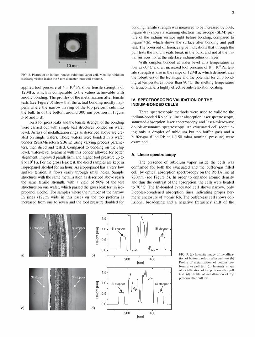
The final cell is shown in Figure 2.
III. MECHANICAL VALIDATION OF THE BONDINGPROCESS
Tensile tests carried out with samples bonded on chip
level (i.e., containing metallic Rb) at 140 �C and with an
FIG. 1. Schematic of alkali cell fabrication and thermocompression sealing.
2
applied tool pressure of 4� 105 Pa show tensile strengths of
12 MPa, which is comparable to the values achievable with
anodic bonding. The profiles of the metallization after tensile
tests (see Figure 3) show that the actual bonding mostly hap-
pens where the narrow In ring of the top preform cuts into
the bulk In of the bottom around 300 lm position in Figure
3(b) and 3(d).
Tests for gross leaks and the tensile strength of the bonding
were carried out with simple test structures bonded on wafer
level. Arrays of metallization rings as described above are cre-
ated on single wafers. Those wafers were bonded in a wafer
bonder (SussMicrotech SB6 E) using varying process parame-
ters, then diced and tested. Compared to bonding on the chip
level, wafer-level treatment with this bonder allowed for better
alignment, improved parallelism, and higher tool pressure up to
8� 105 Pa. For the gross leak test, the diced samples are kept in
isopropanol alcohol for an hour. As isopropanol has a very low
surface tension, it flows easily through small holes. Sample
structures with the same metallization as described above reach
the same tensile strength, with a yield of 96% of the test
structures on one wafer, which passed the gross leak test in iso-
propanol alcohol. For samples where the number of the narrow
In rings (12lm wide in this case) on the top preform is
increased from one to seven and the tool pressure doubled for
bonding, tensile strength was measured to be increased by 50%.
Figure 4(a) shows a scanning electron microscope (SEM) pic-
ture of the indium surface right before bonding, compared to
Figure 4(b), which shows the surface after bonding and pull
test. The observed differences give indications that through the
pull tests the indium seals break in the bulk, and not at the ini-
tial surfaces nor at the interface indium-adhesion layer.
With samples bonded at wafer level at a temperature as
low as 60 �C and an increased tool pressure of 8� 105 Pa, ten-
sile strength is also in the range of 12 MPa, which demonstrates
the robustness of the technique and the potential for chip bond-
ing at temperatures lower than 80 �C, the melting temperature
of tetracontane, a highly effective anti-relaxation coating.
IV. SPECTROSCOPIC VALIDATION OF THEINDIUM-BONDED CELLS
Three spectroscopic methods were used to validate the
indium-bonded Rb cells: linear absorption laser spectroscopy,
saturated-absorption laser spectroscopy and laser-microwave
double-resonance spectroscopy. An evacuated cell (contain-
ing only a droplet of rubidium but no buffer gas) and a
buffer-gas filled Rb cell (150 mbar nominal pressure) were
examined.
A. Linear spectroscopy
The presence of rubidium vapor inside the cells was
confirmed for both the evacuated and the buffer-gas filled
cell, by optical absorption spectroscopy on the Rb D2 line at
780 nm (see Figure 5). In order to enhance atomic density
and thus the contrast of the absorption, the cells were heated
to 70 �C. The In-bonded evacuated cell shows narrow, only
Doppler-broadened absorption lines indicating proper her-
metic enclosure of atomic Rb. The buffer-gas cell shows col-
lisional broadening and a negative frequency shift of the
FIG. 2. Picture of an indium-bonded rubidium vapor cell. Metallic rubidium
is clearly visible inside the 5 mm diameter inner cell volume.
FIG. 3. (a) Intensity image of metalliza-
tion of bottom preform after pull test (b)
Profile of metallization of bottom pre-
form after pull test. (c) Intensity image
of metallization of top preform after pull
test. (d) Profile of metallization of top
preform after pull test.
3

absorption lines (both in the order of few MHz/mbar),19
which confirms the presence of buffer-gas in this cell.
B. Saturated-absorption spectroscopy
Saturated-absorption spectroscopy20 was performed on
the evacuated cell in order to assess the cleanliness of the
bonding process. Analyzing the width of the narrow
Doppler-free lines (down to 6 MHz for a non-contaminated
cell) allows to measure gas pressure inside the cell on the
order of 1 mbar or below (assuming nitrogen gas contamina-
tion). Figure 6 shows the saturated-absorption spectrum for
an indium-bonded cell (60 �C cell temperature) recorded 2
months after sealing, and for a cm-scale glass-blown cell
serving as reference, recorded under similar experimental
conditions. Compared to the linewidth Cref obtained from the
glass-blown reference cell, which is limited by optical power
broadening and the linewidth of the interrogating laser, the
In-bonded cell showed an additional broadening of CIn �Cref¼ 15(4) MHz with respect to the cm-scale reference cell.
This additional broadening can be interpreted as being due to
gas contamination of the vapor cell. Since He and N2, the
most probable contaminants, have broadening coefficients
of�15 MHz/mbar,19 the gas contamination of the cell is esti-
mated to be�1 mbar. Such gas pressures are high enough to
significantly degrade the clock-transition linewidth in a cm-
scale wall-coated vapor cell.21 The same measurement was
repeated 5 months after fabrication and no further broaden-
ing was detected, thus maintaining the same upper limit for a
potential contamination. From the 4 MHz uncertainty of the
linewidth result we derive an upper limit for a potential leak
rate of 3� 10�13 mbar�l/s.
C. Double-resonance spectroscopy
Laser-pumped double-resonance spectroscopy2,22 was
performed on a cell containing both Rb and a buffer-gas mix-
ture (150 mbar pressure), to demonstrate the suitability of
the cell for clock applications and to evaluate the leak rate of
the In bonding. The cell was mounted on a double-resonance
spectroscopy setup22 to retrieve the resonance signal of the
52S1/2 |F¼ 1, mF¼ 0i!|F¼ 2, mF¼ 0i clock transition. The
setup (see Figure 7) consists of a compact, frequency-
stabilized laser head that emits light resonant with the Rb D2
line at 780 nm, and a magnetron-type microwave cavity reso-
nant at 6.834 GHz containing the cell under test. The micro-
wave cavity is used to apply the microwave magnetic field to
the atoms and is excited by a commercial synthesizer. The
microwave cavity is also surrounded by a solenoid (C-field
coil) in order to apply a static magnetic field, creating the
quantization axis, and at the same time, isolating the “clock”
transition by Zeeman splitting. The whole is surrounded by
two layers of mu-metal magnetic shields to reduce the effect
FIG. 4. SEM pictures of indium surface (a) before bonding and (b) after
bonding and pull test.
FIG. 5. Optical absorption spectra of two different In-bonded cells (bottom
graph), compared to a reference cell (top graph). Broadening and shift of the
absorption lines of the buffer-gas cell are due to the buffer-gas inside the cell.
FIG. 6. Saturated-absorption spectrum of an indium-bonded cell (lower
trace) compared to the one of a cm-scale glass-blown reference cell (upper
trace). Circles mark the saturated-absorption line of the 87Rb F¼ 2! F0 ¼ 3
transition. Note that the strong saturated-absorption lines present for the cm-
scale reference cell (cross-over resonances located at �133 and �211 MHz)
are not observed in the In-bonded cell here.
4

of external magnetic field fluctuations. The clock signal—as
shown in the inset of Figure 8—is obtained by recording the
light intensity transmitted through the cell while sweeping
the microwave frequency. The signal linewidth extrapolated
to zero light intensity is 2.022(7) kHz, only slightly higher
than the predicted intrinsic linewidth of 1.6 kHz for our cell
design,10 most probably due to power broadening by the
microwave field. The measured 16.8 kHz shift of the clock
signal, as compared to the unperturbed resonance frequency,
is in good agreement with the calculated shift of 16 kHz
expected for the buffer-gas mixture ratio r theoretically filled
into the cell (r ¼ PAr=PN2¼ 1:3, Ptot ¼ 150 mbar, in this
case),23 which shows good control of the filling procedure. A
correction factor for the non-uniformity of the gas density
within the filling chamber during cell sealing due to tempera-
ture differences between the cell and the pressure gauge was
taken into account when calculating the shift.
V. LEAK RATE CHARACTERIZATION
In the presence of a leak with leak-rate L, the evolution of
the pressure P inside a cell is proportional to the difference of
internal and external pressures and can be expressed by
dP
dt¼ L
PnormV0
ðPext � PÞ; (1)
where V0 is the volume of the cell cavity, Pnorm a normaliza-
tion pressure of 1000 mbar, and Pext the external pressure at
which the sample is kept (1000 mbar in our case). The pres-
sure evolution is then
PðtÞ ¼ Pext � ðPext � P0Þ � e�ðLt=VPnormÞ; (2)
where P0 is the initial pressure inside the cell at t¼ 0. Since
the expected pressure variations are small compared to the
external pressure, a linear approximation can be made giving
a much simpler expression for L
L ¼ VDp
Dt: (3)
Frequency aging or drift of a miniature atomic clock
should be on the level of 10�11/day or less, which in the case
of Rb and N2 and our 15 ll cell volume corresponds to a leak
rate of 5� 10�14 mbar�l/s (i.e., a total pressure change of 1
mbar over a 10 years lifetime). Such leak rates are difficult
to measure over short periods of time; for example, the mini-
mum leak rate measureable with standard helium leak test
devices is on the order of 10�11 mbar�l/s. We therefore used
two alternative methods to characterize the tightness of the
In-bonding over time.
The first method was mechanical; it is based on the mea-
sure of the deflection of a Si membrane24 integrated into
dedicated cell samples. If the deflection is small compared to
the size of the membrane, the membrane deflection can be
linked to the pressure difference PD¼Pext � P between the
two sides of the membrane. Using the analytical model of
Bonnotte,25 and assuming zero residual stress in the mem-
brane, this difference is expressed as follows:
PD ¼ C1
bd3
a4
E
ð1� �Þ þ C2
E
ð1� �2Þb3d
a4; (4)
where E is the Young’s modulus and � the Poisson ratio, b
the thickness of the membrane, d the maximum deflection,
and a half the side length of the square membrane. C1 and C2
are coefficients that depend on the shape and material of the
membrane. In the case of a square membrane, we use
C1¼ 1.84 and C2¼ 4.129, derived from the coefficients
given by Timoshenko26 for a thin square membrane with
small deflections. Knowing the pressure outside the cavity
Pext, which corresponds to the atmospheric pressure, the in-
ternal pressure can be deduced from Equation (4). Assuming
atmospheric pressure known within 0.1 mbar and the deflec-
tion within 10 nm, the detection limit for pressure changes
would be about 1 mbar. The membrane deflections as well as
the atmospheric pressure during the measurements were
recorded right after bonding of the sample cells and there-
after every few weeks.
In order to observe a reasonably large membrane deflec-
tion, sample structures with thin membranes are prepared.
They are fabricated by KOH etching of arrays of squares on a
525 lm silicon wafer. The wafers are removed from the etch
bath when the membranes reach a thickness of about 40 lm
with a side length close to 3 mm. The wafer with the cavities
is bonded to a silicon wafer using the same metallization and
the same bonding parameters as described above; the wafer
FIG. 7. Double-resonance atomic clock setup used for the experiments.
FIG. 8. Linewidth of the double-resonance clock signal of the In-bonded
cell with buffer gas. The linewidth extrapolated to zero light intensity is
2022(7) Hz. The inset shows an example of the clock signal.
5

stack is then diced into 10� 10 mm2 chips. Since the bonding
is done under vacuum, the membrane is deflected when
exposed to ambient pressure as shown in Figure 9.
A white light interferometer (Wyko NT1100) was used
to measure the deflection of the membranes, with measure-
ments taking place over several months. No evident decrease
in membrane deflection was observed over several months
although the dependency of the deflection along with the
atmospheric pressure Pext could be seen easily. The pressure
P inside the cavity was calculated by taking into account the
variations of the atmospheric pressure over 5 months. The
variation of the internal pressure was 1 mbar overall peak-to-
peak value, with no trend observable. Taking into account
the limited accuracy of both the interferometer (about
10 nm) and the atmospheric pressure sensor, we get a maxi-
mum change of 2 mbar over 5 months, which corresponds to
a leak rate of 2.2� 10�12 mbar�l/s. This is to be considered
as an upper limit to a potential leak rate of the cells; meas-
urements over longer time range are expected to further
reduce this limit.
The second method was based on DR spectroscopy of a
BG filled In-bonded cell. In addition to its quenching and
anti-relaxation properties, the presence of a BG mixture also
induces a shift from the unperturbed frequency on the micro-
wave clock transitions that are proportional to each relative
pressures of the gas considered23
D�tot ¼X
i
D�i ¼X
i
Piðbi þ diDT þ ciDT2Þ; (5)
where the indices i refer to the different BG considered, D�i
is the induced shift, Pi the partial gas pressure, and bi, di, and
ci are coefficients proper to the gas and alkali atom consid-
ered. Thus, for identical experimental conditions, any
income of buffer gas would lead to a shift proportional to the
variation of the internal pressure. For a cell kept in air, one
can assume that only nitrogen participates to an internal pres-
sure increase, with a nitrogen pressure-shift coefficient of
b¼ 411 Hz/mbar (Ref. 27), since oxygen—the second most
probable contaminating gas—would immediately react with
the alkali atoms. In order to correct for shifts caused by the
light-atom interaction and extract the cell’s intrinsic shift, a
linear extrapolation of the clock frequency to zero light in-
tensity was done for each measurement.
The clock frequency shift extrapolated to zero light in-
tensity in the In-bonded cell was measured four times over
the timespan of one year, and each point was then scaled to a
pressure deviation from the first data point (see Figure 10),
assuming a cell contamination by nitrogen only. The error
bars include systematic shifts due to the positioning
uncertainty of the cell inside the microwave resonator that
may lead to varying microwave power shifts. However, an
upper limit for a potential leak rate of the cells can still
be estimated. Using the maximum pressure variation of
�0.28 mbar over one year, we obtain a maximum leak rate
of 1.5� 10�13 mbar�l/s.
VI. DISCUSSION
All reported leak rate measurements for the In-bonded
cells are in good agreement with each other, giving upper
limits of 2� 10�12 to 1.5� 10�13 mbar�l/s. An increase in
gas pressure within a sealed cell can have different origins:
outgassing from the cell walls, flow of atmospheric gases
into the cavity through potential micro-leaks in the bonding
structure or cell walls, or permeation of gases (in particular
He) through the cell walls.
If a pressure increase is measured right after bonding, it
is most probably due to outgassing of trapped gases at the
surfaces or in the bulk of the materials used, which are liber-
ated at the bonding temperatures. Such outgassing can be
limited by performing an outgassing step with the preforms
before bonding. As the melting temperature of indium is
very low, this step was not performed for the fabrication of
the alkali cells presented in this paper, which could explain
the small but non-zero gas pressure after bonding reported in
Sec. IV B. In spite of the omitted outgassing, the saturated-
absorption spectroscopy with the evacuated cells confirms a
stable gas contamination of less than 1 mbar, which is ac-
ceptable for alkali buffer-gas cells. For an even cleaner
FIG. 9. (a) Schematic of test structures for optical leak rate testing by mem-
brane deflection measurement. (b) Membrane profile of test vehicles after
bonding in vacuum and exposed to atmospheric pressure measured with a
white light interferometer.
FIG. 10. Evolution of the clock transition frequency expressed as corre-
sponding nitrogen pressure change, recorded at 70 �C over 5 months for a
buffer-gas filled indium-bonded cell. Error bars include systematic uncer-
tainties of the center frequency.
6

atmosphere, an outgassing step below the melting tempera-
ture of indium could be integrated in the process, or a getter
material could be integrated.
If a steady increase of pressure is observed after bond-
ing, it could still originate from outgassing but it might also
arise from a leak of gases surrounding the cell into the sealed
cavity. Even though indium is known as hermetic material,
both the bonding interface and also the interface between the
different metals can be the source for micro-leaks through
which atmospheric gases might enter the cells. If such
micro-leaks are small, small atmospheric gas molecules—
such as He as the smallest gas molecules—may be expected
to be the main source of gas contamination to the cell. In the
case that such micro-leaks are large enough to let pass bigger
atmospheric gas molecules, N2 as the most abundant atmos-
pheric gas is expected to be the main contaminant for the
cell. The clock transition’s pressure shift coefficients for N2
(411 Hz/mbar [Ref. 23]) and for He (540 Hz/mbar [Ref. 27])
differ by about 25% only, but due to the high abundance of
N2 in the atmosphere, the impact of a potential N2 contami-
nation of the cell on the clock frequency is expected to be
dominant, which motivates the analysis in Sec. V. Further-
more, such leakage process should be accompanied by a cell
contamination with O2 and H2O and subsequent oxidation of
the alkali metal. However, oxidation of the rubidium was not
yet observed during the measurements reported in Figure 10.
It has been shown previously that He gas can permeate
through the walls of glass-blown alkali vapor cells, which can
impact the aging behavior of vapor cell atomic clocks,27 while
permeation rates of other atmospheric gases are smaller by
factors of 50 (Ne) to more than 7 orders of magnitude (Ar, O2,
N2).28 This permeation process includes the steps of gas
adsorption on the wall surface, its solution in and diffusion
through the cell walls, and finally desorption from the inner
cell walls.28 Table I summarizes the key parameters for He
permeation through Pyrex glass and Si (the two main materi-
als used in our cells), i.e., the solubility S, diffusion constant
D, and Permeation rate K¼ S�D,29 for a temperature of
T¼ 100 �C. As permeation of He through Si is smaller by
many orders of magnitude compared to permeation through
Pyrex, it is negligible here. It is therefore sufficient to treat the
permeation through the Pyrex windows only.
For the 15 ll volume cell design studied here, the total
Pyrex window surface is 0.4 cm2 and it can be estimated30
that the total He permeation leak rate through the windows is
LHe� 2� 10�9 mbar�l s�1. For the model case of a more
drastically miniaturized 1 ll volume cell with 1 mm2 window
surface, the total He permeation leak rate is expected to be
LHe� 1� 10�10 mbar�l s�1. Using Eqs. (2) and (3), the initial
pressure change rate DP/Dt (using the partial atmospheric He
pressure Pext¼ 5.3� 10�3 mbar) and the He permeation time
constant sHe¼V Pnorm/LHe for the He pressure increase in
the cell can be calculated and are given in Table II for the
two cells designs. For our present cell design, we find
sHe¼ 72 days which is of the same order as reported in
Ref. 27 for cm-scale all-glass cells with 0.5 mm wall thick-
ness. After one year, the total pressure inside our cells due to
He permeation is calculated to be only 1% lower than the
atmospheric He partial pressure, which is far below the pres-
sure change reported in Figure 10. For the case of the 1 ll
cell, the permeation time constant is sHe¼ 96 days.
We thus conclude that a potential pressure increase of
0.28 mbar over one year—the most stringent upper limit
from our measurements—cannot be explained by He perme-
ation through the cell windows, nor by He entering the cell
volume via small leaks as the measured upper limit is far
above the atmospheric He partial pressure. A pressure
increase on this level—if confirmed to be real—needs to be
interpreted as being due to leakage of more abundant atmos-
pheric gases (mainly N2) into the cells or continued outgas-
sing. The small pressure potentially present after cell sealing
(cf. Sec. IV B) can be explained by outgassing during sealing
of the cells.
A decrease in optical or double-resonance signal ampli-
tude would indicate a decrease in the alkali vapor pressure
and could be a sign of rubidium interacting with the metallic
layers or diffusion through it, rather than leakage of water or
oxygen into the cavity. Even though such a decrease in sig-
nal was not yet observed, it cannot be excluded that such
chemical interaction might happen if the cell is kept at the
clock working temperature for longer time. In order to sepa-
rate this effect from a possible gas leakage through the in-
dium seal at elevated temperature, it would be of interest to
conduct leak rate measurements on cells with and without ru-
bidium at higher temperatures.
For the reported studies, the alkali vapor cells were
maintained at room temperature for most of the time and
were only heated up to 70 �C for the spectroscopic meas-
urements. This accumulated to a total of less than 500 h at
elevated temperature. When operating the cells over longer
time at elevated temperature, there might be the possibility
of rubidium diffusing into the indium or reacting slowly with
the metallic seals. This process was not addressed in the
present work and remains to be studied.
TABLE I. Solubility, diffusion constant and permeation rate of He through
Pyrex and crystalline Si, for a temperature of 100 �C. The Si data were
obtained by extrapolating the data of Van Wieringen et al.31
Solubility S(cm3/cm3 at 1 atm)
Diffusion
constant D(cm2 s�1)
Permeation rate K(m2 s�1 Pa�1)
He through Pyrexa 4.3� 10�3 7.0� 10�8 3.0� 10�19
He through Sib 8.5� 10�12 1.1� 10�18 9.2� 10�39
aReference 29.bReference 31.
TABLE II. Calculated initial pressure change rate DP/Dt and permeation
time constant for the 15 ll cell studied here and a hypothetical 1 ll cell. Py-
rex window thickness is 0.5 mm in both cases. Parameters of Table I were
used.
Cell design
Initial pressure
change rate DP/Dt
He permeation
time constant sHe
15 ll cell (see Sec. II) 7.3� 10�5 mbar/day 72 days
1 ll cell 5.5� 10�5 mbar/day 96 days
7

VII. CONCLUSION
We have demonstrated the fabrication and evaluation of
micro-fabricated alkali vapor cells, sealed by thin-film indium
thermo-compression bonding. This technique yields tensile
strengths of the resulting bond comparable to the commonly
used anodic bonding technique. Results from optical spectros-
copy confirm a stable and sufficiently clean atmosphere inside
the cell, in spite of the somewhat limited compatibility of the
indium bonding technique with outgassing of the preforms
before bonding (due to the low melting temperature of in-
dium). A consistent upper limit of 1 mbar was found for a
potential gas contamination inside the cells during the sealing
and over the time of several months, proving a clean process
and also the good hermeticity of the indium bonding.
The suitability of the cells for atomic clock applications
was demonstrated by recording double-resonance signals for a
buffer-gas filled In-bonded cell. The retrieved clock signal line-
width is 2.02 kHz, only slightly higher than the theoretically
predicted intrinsic linewidth for this cell. The center frequency
of the cell was recorded several times over the course of one
year, giving an upper limit of 1.5� 10�13 mbar�l/s�1 for a
potential leak rate. This result is compatible with the results
obtained from the membrane deflection method performed on
samples without alkali metal present. An analysis of He perme-
ation through the cell walls shows that this process corresponds
to a pressure variation in the cell around 3 orders of magnitude
smaller than our experimental upper limit.
The low-temperature hermetic sealing technique demon-
strated here presents a clear improvement compared to previ-
ously reported low-temperature sealing techniques. With
sealing temperatures below 140 �C, thin-film indium sealing is
already compatible with anti-relaxation coatings such as OTS,
and opens the way towards microfabricated wall-coated alkali
vapor cells for applications such as atomic clocks or magneto-
meters. By exploiting the demonstrated higher bonding pres-
sures up to 8� 105 Pa, cell sealing at temperatures below the
melting temperature of micro-fabricated alkali cells with
paraffin-type wall-coatings is also expected to be possible.
ACKNOWLEDGMENTS
This work was supported by the Swiss National Science
Foundation (Sinergia Grant No. CRSI20-122693/1). The
authors thank the CMI and the CSEM Microsystems Technol-
ogy Division staff and all the Sinergia project partners for
their contributions and help. They also acknowledge the con-
tributions from C. Schori and P. Thomann at the early stages
of the project.
1S. Knappe, Comprehensive Microsyst. 3, 571 (2008).2J. Camparo, Phys.Today 60(11), 33 (2007).3L.-A. Liew, S. Knappe, J. Moreland, H. Robinson, L. Hollberg, and
J. Kitching, Appl. Phys. Lett. 84, 2694 (2004).4K. Tsujimoto, Y. Hirai, K. Sugano, T. Tsuchiya, and O. Tabata, in
Proceedings of the 25th IEEE International Conference on Micro ElectroMechanical Systems, MEMS 2011, Cancun, Mexico, 23–27 January 2011,
pp. 368–371.5Y. W. Yi, H. G. Robinson, S. Knappe, J. E. Maclennan, C. D. Jones,
C. Zhu, N. A. Clark, and J. Kitching, J. Appl. Phys. 104, 023534
(2008).6G. Robinson and C. E. Johnson, Appl. Phys. Lett. 40, 771 (1982).7D. Budker, L. Hollberg, D. F. Kimball, J. Kitching, S. Pustelny, and V. V.
Yashchuk, Phys. Rev. A 71, 012903 (2005).8S. J. Seltzer, D. M. Rampulla, S. Rivillon-Amy, Y. J. Chabal, S. L. Berna-
sek, and M. V. Romalis, J. Appl. Phys. 104, 103116 (2008).9T. Bandi, C. Affolderbach, and G. Mileti, J. Appl. Phys. 111, 124906
(2012).10J. Kitching, S. Knappe, and L. Hollberg, Appl. Phys. Lett. 81, 553 (2002).11A. Douahi, M. Hasegawa, L. Nieradko, J. J. Boy, C. Gorecki, and V. Gior-
dano, in Proceedings of the 22nd European Frequency and Time Forum(EFTF), Toulouse, France, 22–25 April 2008, FPE-0061.
12C. Rahman and H. Robinson, IEEE J. Quantum Electron. 23, 452 (1987).13S. J. Seltzer and M. V. Romalis, J. Appl. Phys. 106, 114905 (2009).14Y. P�etremand, C. Schori, R. Str€assle, G. Mileti, N. de Rooij, and P. Tho-
mann, in Proceedings of at the 2010 European Frequency and Time Forum
(EFTF), Noordwijk, Netherlands, 13–16 April 2010, P119.15R. Straessle, M. Pellaton, Y. P�etremand, C. Affolderbach, D. Briand,
G. Mileti, and N. F. de Rooij, in Proceedings of the 26th IEEE Interna-tional Conference on Micro Electro Mechanical Systems, MEMS 2012,
Paris, 29 January – 2 February 2012, pp. 361–364.16R. Straessle, Y. Petremand, D. Briand, N. F. de Rooij, M. Pellaton,
C. Affolderbach, and G. Mileti, in Proceedings of the IEEE InternationalFrequency Control Symposium (FCS), Baltimore, MD, USA, 21–24 May
2012, pp. 127–130.17J. Kim, H. Schoeller, J. Cho, and S. Park, J. Electron. Mater. 37, 483
(2008).18V. Simic and �Z. Marinkovic, Thin Solid Films 41, 57 (1977).19M. D. Rotondaro and G. P. Perram, J. Quant. Spectrosc. Radiat. Transfer
57, 497 (1997).20S. A. Knappe, H. G. Robinson, and L. Hollberg, Opt. Express 15, 6293
(2007).21S. Knappe and H. G. Robinson, New J. Phys. 12, 065021 (2010).22M. Pellaton, C. Affolderbach, G. Mileti, Y. P�etremand, and N. F. de Rooij,
in Proceedings of the 2011 Joint Meeting of the European Frequency andTime Forum (EFTF) and the IEEE International Frequency Control Sym-posium (IFCS), San Francisco, CA, 2–5 May 2011, pp. 604–606.
23J. Vanier, R. Kunski, N. Cyr, J. Y. Savard, and M. Tetu, J. Appl. Phys. 53,
5387 (1982).24D. Lellouchi, J. Dhennin, X. Lafontan, D. Veyrie, J.-F. L. Neal, and
F. Pressecq, J. Micromech. Microeng. 20, 025031 (2010).25E. Bonnotte, P. Delobelle, L. Bornier, B. Trolard, and G. Tribillon, J. Mat.
Res 12, 2234–2248 (1997).26S. P. Timoshenko and S. Woinowsky-Krieger, Theory of Plates and Shells,
2nd ed. (McGraw-Hill, New York, NY, 1959).27J. C. Camparo, C. M. Klimcak, and S. J. Herbulock, IEEE Trans. Instrum.
Meas. 54, 1873 (2005).28F. J. Norton, J. Appl. Phys. 28, 34 (1957).29K. Kawasaki and K. Senzaki, Jap. J. Appl. Phys. 1, 223 (1962).30G. L. Harding, Sol. Energy Mater. 5, 141 (1981).31A. Van Wieringen and N. Warmoltz, Physica 22, 849 (1956).
8