low voltage 16-bit constant current led sink driver · april 2017 docid18469 rev 6 1/28 this is...
TRANSCRIPT
April 2017 DocID18469 Rev 6 1/28
This is information on a product in full production. www.st.com
STP16CPC26
Low voltage 16-bit constant current LED sink driver
Datasheet - production data
Features 16 constant current output channels
Adjustable output current through external resistor
Output current: 5 mA to 90 mA
±1% typical current accuracy bit to bit
Max clock frequency: 30 MHz
20 V current generators rated voltage
3 - 5.5 V power supply
Thermal shutdown for overtemperature protection
Applications Video display panel LED driver
Special lighting
Description The STP16CPC26 is a monolithic, low voltage, 16-bit constant current LED sink driver. The device contains a 16-bit shift register and data latches, which convert serial input data into parallel output format. In the output stage sixteen regulated current generators provide 5 mA to 90 mA constant current to drive LEDs. The current is externally adjusted through a resistor. LED brightness can be adjusted from 0% to
100% via OE pin.
The STP16CPC26 guarantees a 20 V driving capability, allowing users to connect more LEDs in series to each current source.
The high 30 MHz clock frequency makes the device suitable for high data rate transmission.
The thermal shutdown (170 °C with about 15 °C hysteresis) assures protection from overtemperature events.
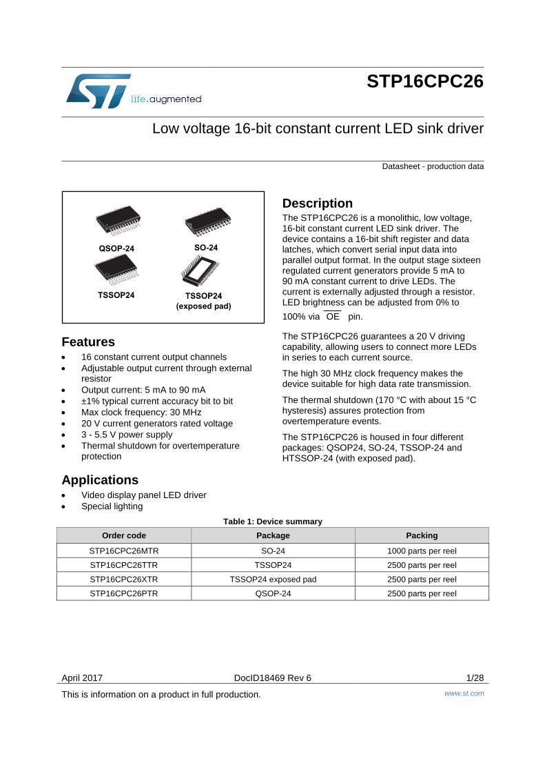
The STP16CPC26 is housed in four different packages: QSOP24, SO-24, TSSOP-24 and HTSSOP-24 (with exposed pad).
Table 1: Device summary
Order code Package Packing
STP16CPC26MTR SO-24 1000 parts per reel
STP16CPC26TTR TSSOP24 2500 parts per reel
STP16CPC26XTR TSSOP24 exposed pad 2500 parts per reel
STP16CPC26PTR QSOP-24 2500 parts per reel
Contents STP16CPC26
2/28 DocID18469 Rev 6
Contents
1 Pin description ................................................................................ 3
2 Electrical ratings ............................................................................. 4
2.1 Absolute maximum ratings ................................................................ 4
2.2 Thermal data ..................................................................................... 4
3 Electrical characteristics ................................................................ 5
4 Simplified internal block diagram .................................................. 8
5 Typical application circuit ............................................................... 8
6 Equivalent circuit and outputs ....................................................... 9
7 Typical test circuits ....................................................................... 11
8 Timing diagrams ............................................................................ 12
9 Current generators characteristics .............................................. 15
9.1 Current setting ................................................................................. 15
9.2 Current accuracy ............................................................................. 15
9.3 Generators voltage drop ................................................................. 16
10 Thermal shutdown ......................................................................... 16
11 Package information ..................................................................... 17
11.1 QSOP-24 package information ....................................................... 18
11.2 SO-24 package information ............................................................ 20
11.3 TSSOP24 package information ....................................................... 21
11.4 TSSOP24 exposed pad package information ................................. 23
11.5 TSSOP24, TSSOP24 exposed pad and ............................................
SO-24 packing information .............................................................. 25
12 Revision history ............................................................................ 27
STP16CPC26 Pin description
DocID18469 Rev 6 3/28
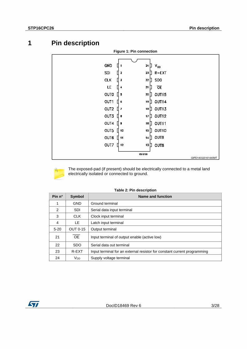
1 Pin description Figure 1: Pin connection
The exposed-pad (if present) should be electrically connected to a metal land electrically isolated or connected to ground.
Table 2: Pin description
Pin n° Symbol Name and function
1 GND Ground terminal
2 SDI Serial data input terminal
3 CLK Clock input terminal
4 LE Latch input terminal
5-20 OUT 0-15 Output terminal
21 OE Input terminal of output enable (active low)
22 SDO Serial data out terminal
23 R-EXT Input terminal for an external resistor for constant current programming
24 VDD Supply voltage terminal

Electrical ratings STP16CPC26
4/28 DocID18469 Rev 6
2 Electrical ratings
2.1 Absolute maximum ratings
Stressing the device above the rating listed in the “absolute maximum ratings” table may cause permanent damage to the device. These are stress ratings only and operation of the device at these or any other conditions above those indicated in the operating sections of this specification is not implied. Exposure to absolute maximum rating conditions for extended periods may affect device reliability.
Table 3: Absolute maximum ratings
Symbol Parameter Value Unit
VDD Supply voltage 0 to 7 V
VO Output voltage -0.5 to 20 V
IO Output current 90 mA
VI Input voltage -0.4 to VDD+0.4 V
IGND GND terminal current 1600 mA
ESD Electrostatic discharge protection HBM human body model ±2 kV
fCLK Clock frequency 30 MHz
2.2 Thermal data
Table 4: Thermal data
Symbol Parameter Value Unit
TA Operating free-air temperature range -40 to +125 °C
TOPR Operating temperature range -40 to +150 °C
TSTG Storage temperature range -55 to +150 °C
RthJA Thermal resistance junction-ambient(1)
SO-24 60 °C/W
TSSOP24 85 °C/W
TSSOP24 (2)
exposed pad 37.5 °C/W
QSOP-24 72 °C/W
Notes:
(1) According with JEDEC standard 51-7. (2) The exposed pad should be soldered directly to the PCB to realize the thermal benefits.
STP16CPC26 Electrical characteristics
DocID18469 Rev 6 5/28
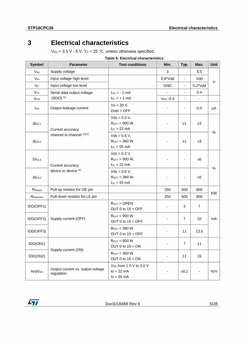
3 Electrical characteristics
VDD = 3.3 V - 5 V, TA = 25 °C, unless otherwise specified.
Table 5: Electrical characteristics
Symbol Parameter Test conditions Min. Typ. Max. Unit
Vdd Supply voltage
3
5.5
V VIH Input voltage high level
0.8*Vdd - Vdd
VIL Input voltage low level GND - 0.2*Vdd
VOL Serial data output voltage
(SDO) (1)
IOH = - 1 mA
IOL = + 1 mA
- - 0.4
VOH VDD -0.4 - -
IOH Output leakage current Vo = 20 V,
Outn = OFF - - 0.5 µA
ΔIOL1
Current accuracy
channel to channel (2)(3)
Vds = 0.3 V,
REXT = 900 W,
IOL = 22 mA
- ±1 ±3
%
ΔIOL2
Vds = 0.6 V,
REXT = 360 W,
IOL = 55 mA
- ±1 ±3
DIOL3
Current accuracy
device to device (2)
Vds = 0.3 V,
REXT = 900 W,
IOL = 22 mA
- - ±6
%
ΔIOL4
Vds = 0.6 V,
REXT = 360 W,
IOL = 55 mA
- - ±6
RIN(up) Pull-up resistor for OE pin
250 500 800 KW
RIN(down) Pull-down resistor for LE pin
250 500 800
IDD(OFF1)
Supply current (OFF)
REXT = OPEN
OUT 0 to 15 = OFF - 3 7
mA IDD(OFF2) REXT = 900 W
OUT 0 to 15 = OFF - 7 10
IDD(OFF3) REXT = 360 W
OUT 0 to 15 = OFF - 11 13.5
IDD(ON1)
Supply current (ON)
REXT = 900 W
OUT 0 to 15 = ON - 7 11
IDD(ON2) REXT = 360 W
OUT 0 to 15 = ON - 11 15
%/dVDS Output current vs. output voltage regulation
VDS from 1.0 V to 3.0 V
Io = 22 mA
Io = 55 mA
- ±0.1 - %/V

Electrical characteristics STP16CPC26
6/28 DocID18469 Rev 6
Symbol Parameter Test conditions Min. Typ. Max. Unit
%/dVDD Output current vs. supply voltage regulation (4)
Io = 22 mA;
VDS = 0.3 V
Io = 55 mA;
VDS = 0.6 V
- ±1 - %/V
Tsd Thermal shutdown
- 170 - °C
Tsd-hy Thermal shutdown hysteresis (4) - 15 20
Notes:
(1) Specification referred to TJ from -40 °C to +125 °C. Specification over the -40 to +125 °C TJ temperature range are assured by design, characterization and statistical correlation. (2) Tested with just one output ON. (3) ΔIOL+ = ((IOLmax - IOLmean)/ IOLmean)*100, DIOL- = ((IOLmin - IOLmean)/ IOLmean)*100, where IOLmean = (IOLout1+IOLout2+…+IOLout16) / 16. (4) Guaranteed by design.

STP16CPC26 Electrical characteristics
DocID18469 Rev 6 7/28
VDD = 3.3 V - 5 V, Tj = 25 °C, unless otherwise specified.
Table 6: Switching characteristics
Symbol Parameter Conditions Min. Typ. Max. Unit
fclk Clock frequency
- - 30 MHz
tPLH1 CLK - OUTn
Propagation delay time
(“L” to “H”)
VDS = 0.8 V
VIH = VDD
VIL = GND
REXT = 900 Ω
RL = 50 Ω
CL = 10 pF
- 100 -
ns
tPLH2 LE - OUTn - 100 -
tPLH3 OE – OUTn - 100 -
tPLHa CLK - SDO
VDD = 3.3 V - 30 -
tPLHb VDD = 5 V - 20 -
tPHL1 CLK - OUTn Propagation delay time
(“H” to “L”)
- 28 -
tPHL2 LE - OUTn
- 28 -
tPHL3 OE – OUTn
- 25 -
tPHLa CLK - SDO
VDD = 3.3 V - 30 -
tPHLb
VDD = 5 V - 20 -
tw(CLK) CLK Pulse width
20 - -
tw(L) LE
20 - -
tw(OE) OE
150 - -
tsu(L) Setup time for LE 5 - -
th(L) Hold time for LE 5 - -
tsu(D) Setup time for SDI 5 - -
th(D) Hold time for SDI 10 - -
tr (1) Maximum CLK rise time - - 5000
tf (1) Maximum CLK fall time - - 5000
tor1a Output rise time of Vout VIH = VDD,
VIL = GND
VDS = 0.8 V,
RL = 50 Ω
CL = 10 pF
Iout = 22 mA
VDD = 3.3 V - 95 -
tor1b Output rise time of Vout VDD = 5 V - 85 -
tof1a Output fall time of Vout VDD = 3.3 V - 40 -
tof1b Output fall time of Vout VDD = 5 V - 25 -
tor2a Output rise time of Vout VIH = VDD,
VIL = GND
VDS = 0.8 V
RL = 50 Ω
CL = 10 pF
Iout = 55 mA
VDD = 3.3 V - 80 -
tor2b Output rise time of Vout VDD = 5 V - 70 -
tof2a Output fall time of Vout VDD = 3.3 V - 40 -
tof2b Output fall time of Vout VDD = 5 V - 30 -
Iout-ov Output current turn-on overshoot
VDS = 0.6 to 3V
CL = 10 pF
Iout = 5 to 60 mA
- - 0 %
Notes:
(1)If devices are connected in cascade and tr or tf is large, it may be critical to achieve the timing required for data transfer between two cascaded devices.

Simplified internal block diagram STP16CPC26
8/28 DocID18469 Rev 6
4 Simplified internal block diagram Figure 2: STP16CPC26 simplified block diagram
5 Typical application circuit Figure 3: Typical application circuit
STP16CPC26 Equivalent circuit and outputs
DocID18469 Rev 6 9/28
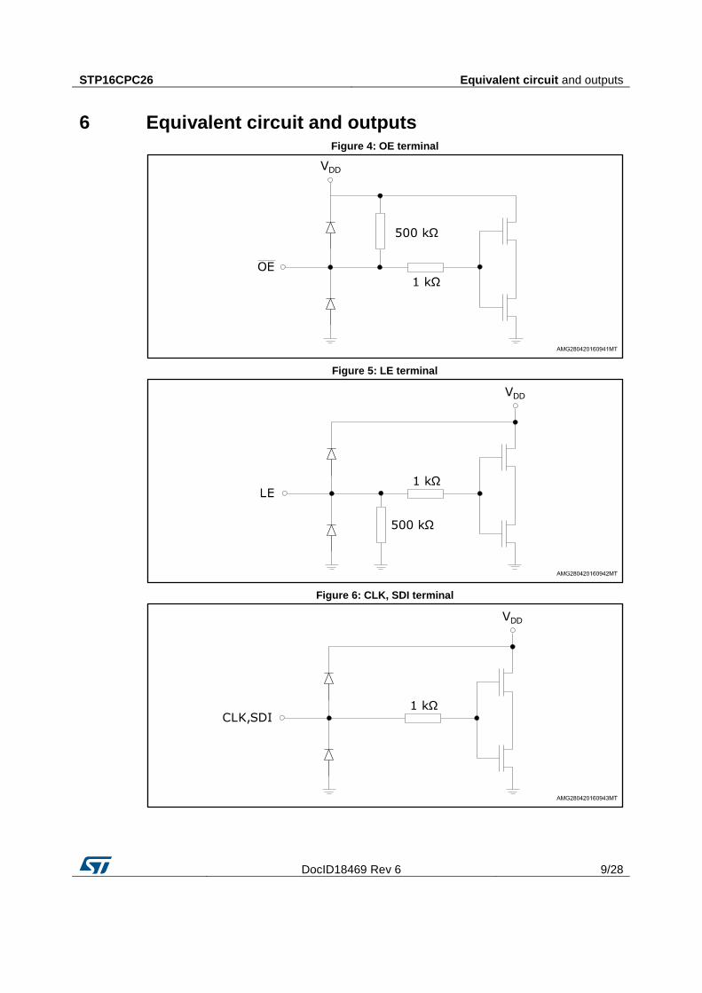
6 Equivalent circuit and outputs Figure 4: OE terminal
Figure 5: LE terminal
Figure 6: CLK, SDI terminal

Equivalent circuit and outputs STP16CPC26
10/28 DocID18469 Rev 6
Figure 7: SDO terminal

STP16CPC26 Typical test circuits
DocID18469 Rev 6 11/28
7 Typical test circuits
Figure 8: "Typical test circuit for electrical characteristics" and Figure 9: "Typical test circuit for switching characteristics" show respectively the typical test circuit used measuring electrical (e.g. input voltage high/low level, output leakage current, supply current, etc.) and switching characteristics (propagation delays, set-up and hold time, rise and fall time of VOUT, etc.). The resistor RL and capacitor CL in parallel connected to each output in Figure 8: "Typical test circuit for electrical characteristics" simulate a LED behavior.
Figure 8: Typical test circuit for electrical characteristics
Figure 9: Typical test circuit for switching characteristics

Timing diagrams STP16CPC26
12/28 DocID18469 Rev 6
8 Timing diagrams
The timing diagram shown in Figure 10: "Timing diagram" and the truth table in Table 7: "Truth table" explain how to send data to the device. This can be summarized in the following points:
LE and OE are level sensitive and not synchronized with the CLK signal
When LE is at low level, the latch circuit holds previous data
If LE is high level, data present in the shift register are latched
When OE is at low level, the status of the outputs OUT0 to OUT15 depends on the
data in the latch circuits
With OE at high level, all outputs are switched off independently on the data stored
in the latch circuits
Every rising edge of the CLK signal, a new data on SDI pin is sampled. This data is loaded into the shift register, whereas a bit is shifted out from SDO
Figure 10: Timing diagram
Table 7: Truth table
Clock LE OE Serial-IN OUT0 ............. OUT7 ................ OUT15 (1) SDO
_|¯ H L Dn Dn ..... Dn - 7 ..... Dn -15 Dn - 15
_|¯ L L Dn + 1 No change Dn - 14
_|¯ H L Dn + 2 Dn + 2 ..... Dn - 5 ..... Dn -13 Dn - 13
¯|_ X L Dn + 3 Dn + 2 ..... Dn - 5 ..... Dn -13 Dn - 13
¯|_ X H Dn + 3 OFF Dn - 13
Notes:
(1) OUTn = ON when Dn = H, OUTn = OFF when Dn = L.
STP16CPC26 Timing diagrams
DocID18469 Rev 6 13/28
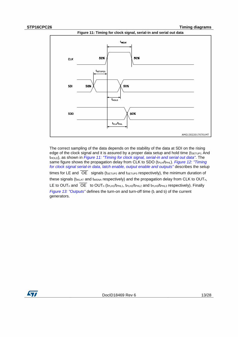
Figure 11: Timing for clock signal, serial-in and serial out data
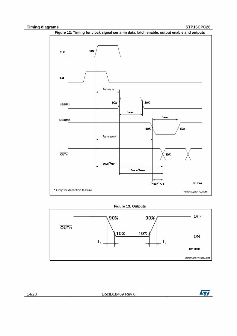
The correct sampling of the data depends on the stability of the data at SDI on the rising edge of the clock signal and it is assured by a proper data setup and hold time (tSETUP1 And tHOLD), as shown in Figure 11: "Timing for clock signal, serial-in and serial out data". The same figure shows the propagation delay from CLK to SDO (tPLH/tPHL). Figure 12: "Timing for clock signal serial-in data, latch enable, output enable and outputs" describes the setup
times for LE and OE signals (tSETUP2 and tSETUP3 respectively), the minimum duration of
these signals (tWLAT and tWENA respectively) and the propagation delay from CLK to OUTn,
LE to OUTn and OE to OUTn (tPLH1/tPHL1, tPLH2/tPHL2 and tPLH3/tPHL3 respectively). Finally
Figure 13: "Outputs" defines the turn-on and turn-off time (tr and tf) of the current generators.
Timing diagrams STP16CPC26
14/28 DocID18469 Rev 6
Figure 12: Timing for clock signal serial-in data, latch enable, output enable and outputs
Figure 13: Outputs
STP16CPC26 Current generators characteristics
DocID18469 Rev 6 15/28
9 Current generators characteristics
9.1 Current setting
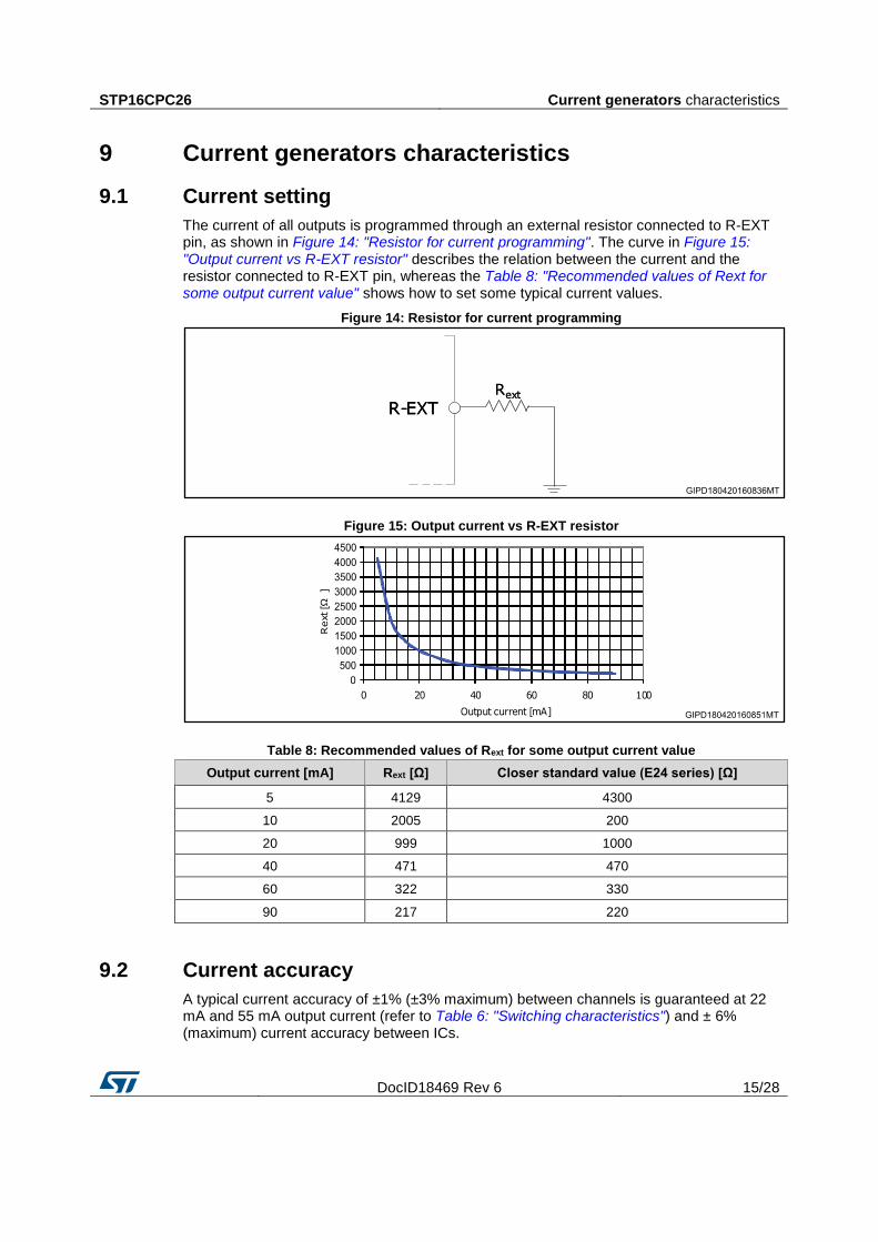
The current of all outputs is programmed through an external resistor connected to R-EXT pin, as shown in Figure 14: "Resistor for current programming". The curve in Figure 15: "Output current vs R-EXT resistor" describes the relation between the current and the resistor connected to R-EXT pin, whereas the Table 8: "Recommended values of Rext for some output current value" shows how to set some typical current values.
Figure 14: Resistor for current programming
Figure 15: Output current vs R-EXT resistor
Table 8: Recommended values of Rext for some output current value
Output current [mA] Rext [Ω] Closer standard value (E24 series) [Ω]
5 4129 4300
10 2005 200
20 999 1000
40 471 470
60 322 330
90 217 220
9.2 Current accuracy
A typical current accuracy of ±1% (±3% maximum) between channels is guaranteed at 22 mA and 55 mA output current (refer to Table 6: "Switching characteristics") and ± 6% (maximum) current accuracy between ICs.
Thermal shutdown STP16CPC26
16/28 DocID18469 Rev 6
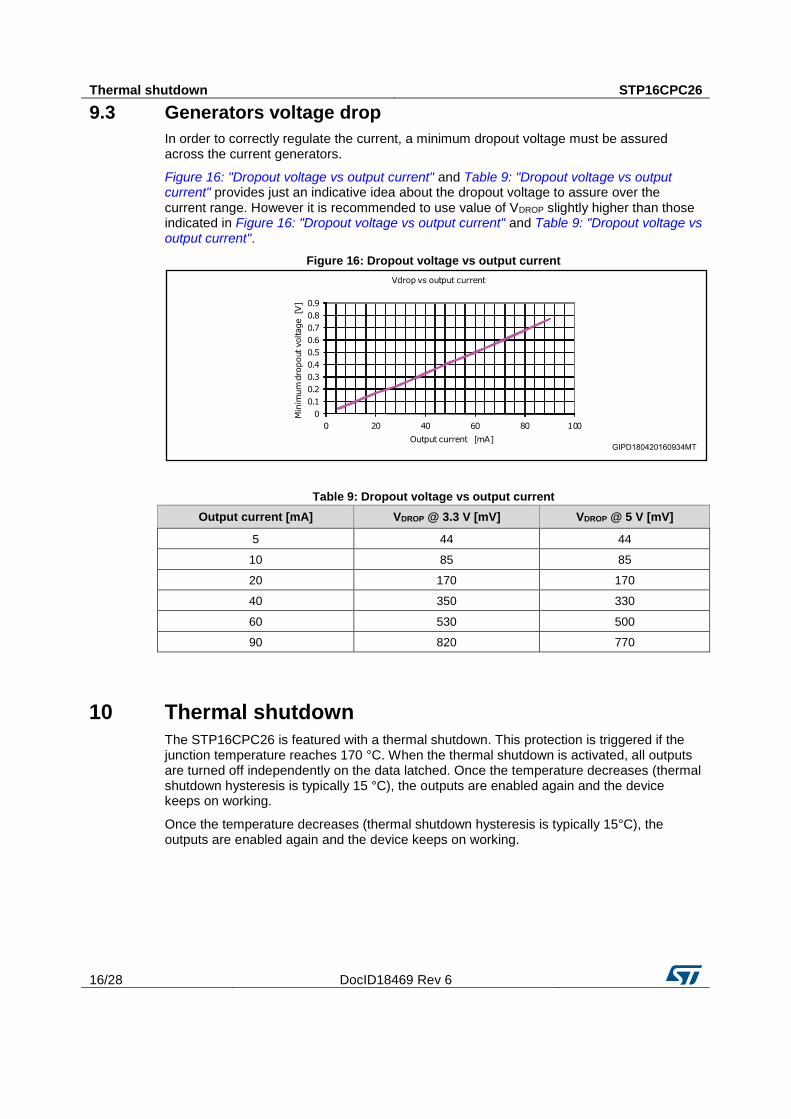
9.3 Generators voltage drop
In order to correctly regulate the current, a minimum dropout voltage must be assured across the current generators.
Figure 16: "Dropout voltage vs output current" and Table 9: "Dropout voltage vs output current" provides just an indicative idea about the dropout voltage to assure over the current range. However it is recommended to use value of VDROP slightly higher than those indicated in Figure 16: "Dropout voltage vs output current" and Table 9: "Dropout voltage vs output current".
Figure 16: Dropout voltage vs output current
Table 9: Dropout voltage vs output current
Output current [mA] VDROP @ 3.3 V [mV] VDROP @ 5 V [mV]
5 44 44
10 85 85
20 170 170
40 350 330
60 530 500
90 820 770
10 Thermal shutdown
The STP16CPC26 is featured with a thermal shutdown. This protection is triggered if the junction temperature reaches 170 °C. When the thermal shutdown is activated, all outputs are turned off independently on the data latched. Once the temperature decreases (thermal shutdown hysteresis is typically 15 °C), the outputs are enabled again and the device keeps on working.
Once the temperature decreases (thermal shutdown hysteresis is typically 15°C), the outputs are enabled again and the device keeps on working.
STP16CPC26 Package information
DocID18469 Rev 6 17/28
11 Package information
In order to meet environmental requirements, ST offers these devices in different grades of ECOPACK® packages, depending on their level of environmental compliance. ECOPACK® specifications, grade definitions and product status are available at: www.st.com. ECOPACK® is an ST trademark.
Package information STP16CPC26
18/28 DocID18469 Rev 6
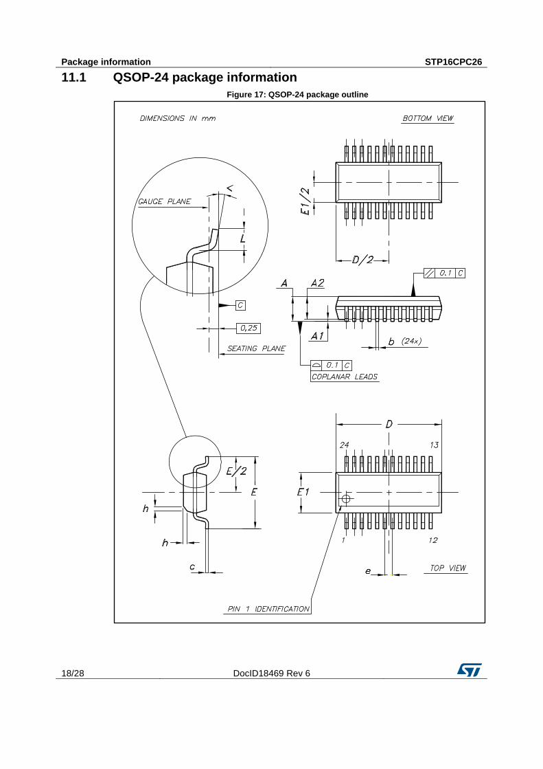
11.1 QSOP-24 package information
Figure 17: QSOP-24 package outline

STP16CPC26 Package information
DocID18469 Rev 6 19/28
Table 10: QSOP-24 mechanical data
Dim. mm
Min. Typ. Max.
A 1.54 1.62 1.73
A1 0.10 0.15 0.25
A2
1.47
b 0.20
0.31
c 0.17
0.254
D 8.56 8.66 8.76
E 5.80 6.00 6.20
E1 3.80 3.91 4.01
e
0.635
L 0.40 0.635 0.89
h 0.25 0.33 0.41
< 0°
8°
Package information STP16CPC26
20/28 DocID18469 Rev 6
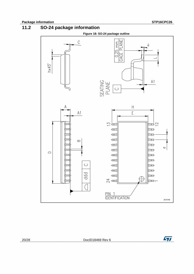
11.2 SO-24 package information
Figure 18: SO-24 package outline

STP16CPC26 Package information
DocID18469 Rev 6 21/28
Table 11: SO-24 mechanical data
Dim. mm
Min. Typ. Max.
A 2.35
2.65
A1 0.10
0.30
B 0.33
0.51
C 0.23
0.32
D 15.20
15.60
E 7.40
7.60
e
1.27
H 10.00
10.65
h 0.25
0.75
L 0.40
1.27
k 0
8
ddd
0.10
11.3 TSSOP24 package information
Figure 19: TSSOP24 package outline
Package information STP16CPC26
22/28 DocID18469 Rev 6
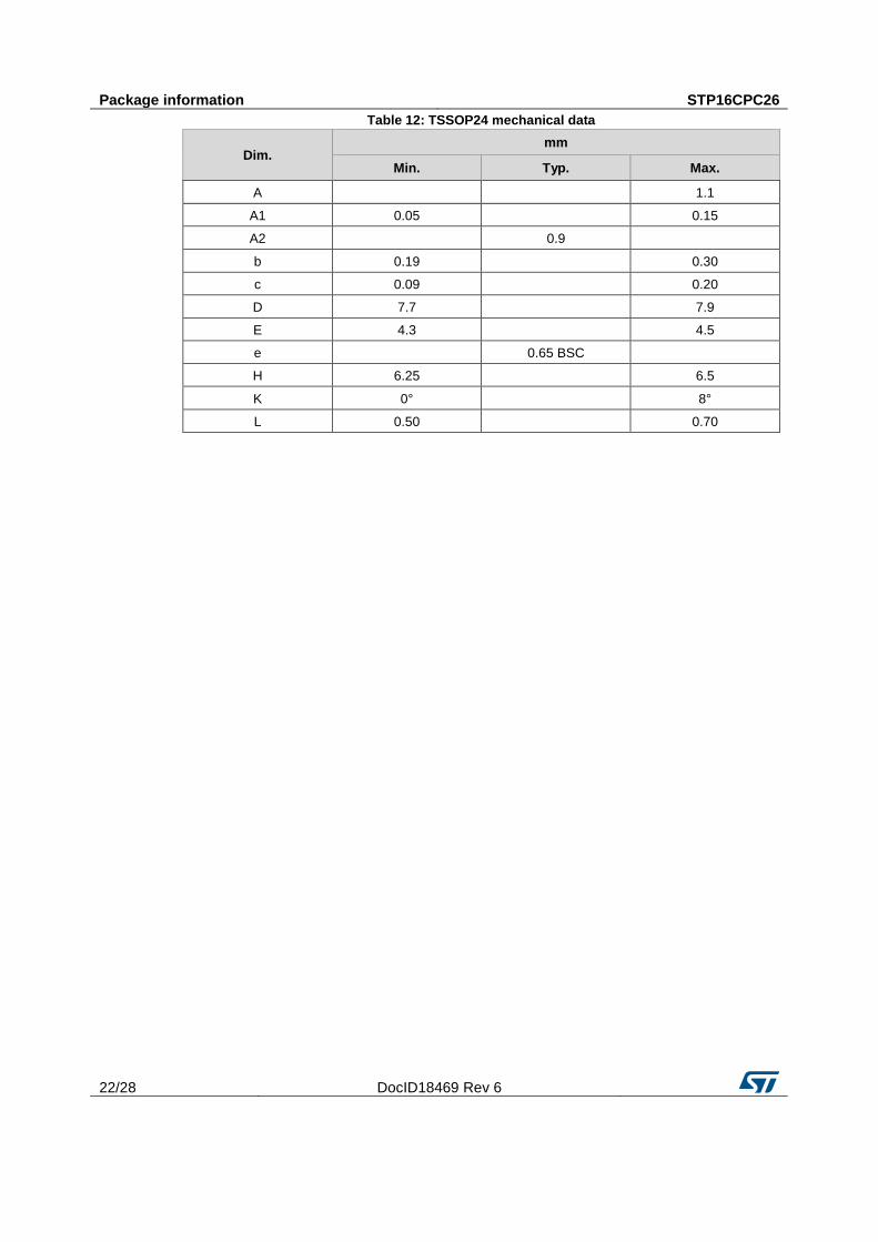
Table 12: TSSOP24 mechanical data
Dim. mm
Min. Typ. Max.
A
1.1
A1 0.05
0.15
A2
0.9
b 0.19
0.30
c 0.09
0.20
D 7.7
7.9
E 4.3
4.5
e
0.65 BSC
H 6.25
6.5
K 0°
8°
L 0.50
0.70
STP16CPC26 Package information
DocID18469 Rev 6 23/28
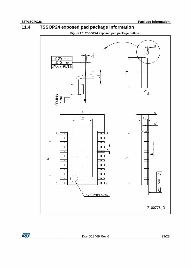
11.4 TSSOP24 exposed pad package information
Figure 20: TSSOP24 exposed pad package outline
Package information STP16CPC26
24/28 DocID18469 Rev 6
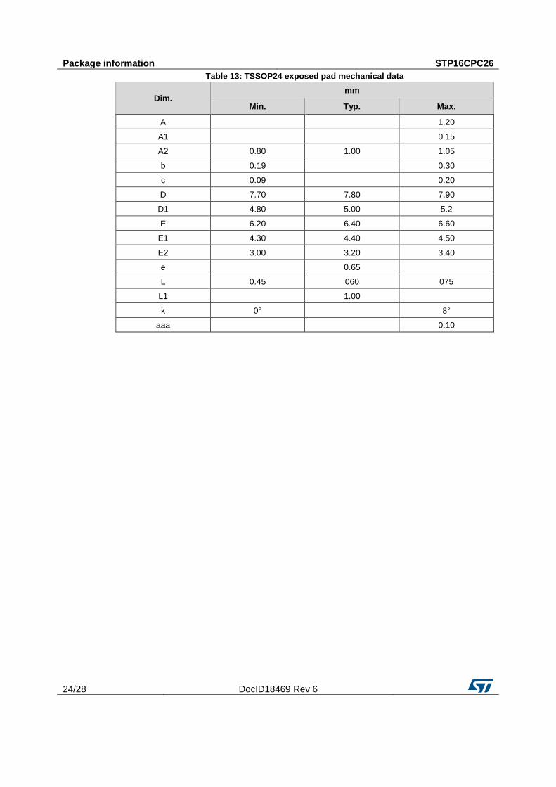
Table 13: TSSOP24 exposed pad mechanical data
Dim. mm
Min. Typ. Max.
A
1.20
A1
0.15
A2 0.80 1.00 1.05
b 0.19
0.30
c 0.09
0.20
D 7.70 7.80 7.90
D1 4.80 5.00 5.2
E 6.20 6.40 6.60
E1 4.30 4.40 4.50
E2 3.00 3.20 3.40
e
0.65
L 0.45 060 075
L1
1.00
k 0°
8°
aaa
0.10

STP16CPC26 Package information
DocID18469 Rev 6 25/28
11.5 TSSOP24, TSSOP24 exposed pad and SO-24 packing information
Figure 21: TSSOP24, TSSOP24 exposed pad and SO-24 reel outline
Table 14: TSSOP24 and TSSOP24 exposed pad tape and reel mechanical data
Dim. mm
Min. Typ. Max.
A
- 330
C 12.8 - 13.2
D 20.2 -
N 60 -
T
- 22.4
Ao 6.8 - 7
Bo 8.2 - 8.4
Ko 1.7 - 1.9
Po 3.9 - 4.1
P 11.9 - 12.1

Package information STP16CPC26
26/28 DocID18469 Rev 6
Table 15: SO-24 tape and reel mechanical data
Dim. mm
Min. Typ. Max.
A
- 330
C 12.8 - 13.2
D 20.2 -
N 60 -
T
- 30.4
Ao 10.8 - 11.0
Bo 15.7 - 15.9
Ko 2.9 - 3.1
Po 3.9 - 4.1
P 11.9 - 12.1

STP16CPC26 Revision history
DocID18469 Rev 6 27/28
12 Revision history Table 16: Document revision history
Date Revision Changes
04-Mar-2011 1 First release
05-Apr-2011 2 Updated Table 6
19-Jul-2012 3 Updated Table 7.
19-Jul-2012 4
Updated characteristics in Table 5: Electrical characteristics and
Table 6: Switching characteristics.
Minor text changes.
1-Jun-2014 5 Updated template and value Table 13: TSSOP24 exposed pad
mechanical data.
13-Apr-2017 6
Updated Figure 11: "Timing for clock signal, serial-in and serial out
data" and Figure 12: "Timing for clock signal serial-in data, latch
enable, output enable and outputs", Section 11.1: "QSOP-24
package information".
Minor text changes.
STP16CPC26
28/28 DocID18469 Rev 6
IMPORTANT NOTICE – PLEASE READ CAREFULLY
STMicroelectronics NV and its subsidiaries (“ST”) reserve the right to make changes, corrections, enhancements, modifications , and improvements to ST products and/or to this document at any time without notice. Purchasers should obtain the latest relevant information on ST products before placing orders. ST products are sold pursuant to ST’s terms and conditions of sale in place at the time of order acknowledgement.
Purchasers are solely responsible for the choice, selection, and use of ST products and ST assumes no liability for application assistance or the design of Purchasers’ products.
No license, express or implied, to any intellectual property right is granted by ST herein.
Resale of ST products with provisions different from the information set forth herein shall void any warranty granted by ST for such product.
ST and the ST logo are trademarks of ST. All other product or service names are the property of their respective owners.
Information in this document supersedes and replaces information previously supplied in any prior versions of this document.
© 2017 STMicroelectronics – All rights reserved