lp5562 four-channel rgb, white-led driver with internal ... · pdf filemcu lp5562 1 p f c in...
TRANSCRIPT
LP5562MCU
1 PFCIN
SCL
SDA
CLK_32K
ADDR_SEL0
ADDR_SEL1
EN/VCC
VDD
GND
R
G
B
-
+
RGB LED 0...25.5 mA/LED
WLED
VDD
Product
Folder
Order
Now
Technical
Documents
Tools &
Software
Support &Community
An IMPORTANT NOTICE at the end of this data sheet addresses availability, warranty, changes, use in safety-critical applications,intellectual property matters and other important disclaimers. PRODUCTION DATA.
LP5562SNVS820B –APRIL 2013–REVISED DECEMBER 2016
LP5562 Four-Channel RGB- or White-LED Driver With Internal Program Memoryand Independent Channel Control
1
1 Features1• Four Independently Programmable LED Outputs
With 8-Bit Current Setting (From 0 mA to 25.5 mAWith 100-μA Steps) and 8-Bit PWM Control
• Typical LED Output Saturation Voltage 60 mV andCurrent Matching 1%
• Flexible PWM Control for LED Outputs• Automatic Power-Save Mode With External Clock• Three Program Execution Engines With Flexible
Instruction Set• Autonomous Operation With Program Execution
Engines• SRAM Program Memory for Lighting Pattern
Programs• DSBGA 12-Pin Package, 0.4-mm Pitch
2 Applications• Fun Lights• Indicator Lights• Keypad RGB Backlighting and Phone Cosmetics
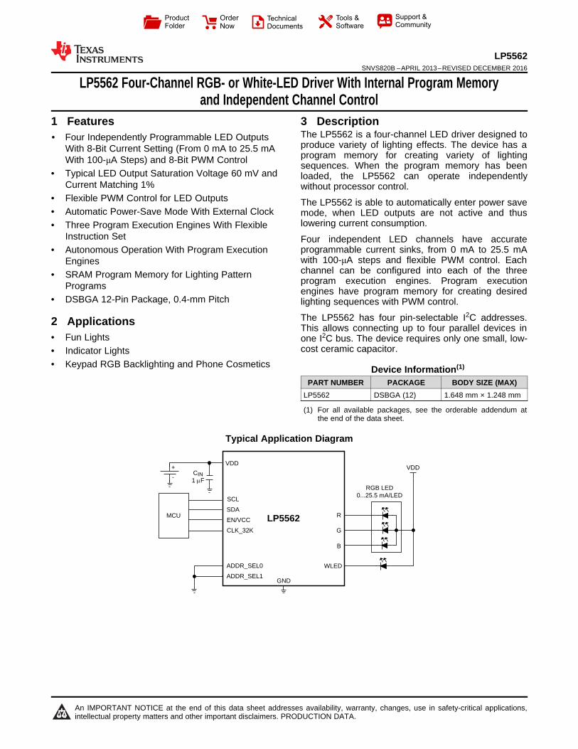
3 DescriptionThe LP5562 is a four-channel LED driver designed toproduce variety of lighting effects. The device has aprogram memory for creating variety of lightingsequences. When the program memory has beenloaded, the LP5562 can operate independentlywithout processor control.
The LP5562 is able to automatically enter power savemode, when LED outputs are not active and thuslowering current consumption.
Four independent LED channels have accurateprogrammable current sinks, from 0 mA to 25.5 mAwith 100-μA steps and flexible PWM control. Eachchannel can be configured into each of the threeprogram execution engines. Program executionengines have program memory for creating desiredlighting sequences with PWM control.
The LP5562 has four pin-selectable I2C addresses.This allows connecting up to four parallel devices inone I2C bus. The device requires only one small, low-cost ceramic capacitor.
Device Information(1)
PART NUMBER PACKAGE BODY SIZE (MAX)LP5562 DSBGA (12) 1.648 mm × 1.248 mm
(1) For all available packages, see the orderable addendum atthe end of the data sheet.
Typical Application Diagram

2
LP5562SNVS820B –APRIL 2013–REVISED DECEMBER 2016 www.ti.com
Product Folder Links: LP5562
Submit Documentation Feedback Copyright © 2013–2016, Texas Instruments Incorporated
Table of Contents1 Features .................................................................. 12 Applications ........................................................... 13 Description ............................................................. 14 Revision History..................................................... 25 Pin Configuration and Functions ......................... 36 Specifications......................................................... 4
6.1 Absolute Maximum Ratings ...................................... 46.2 ESD Ratings.............................................................. 46.3 Recommended Operating Conditions....................... 46.4 Thermal Information .................................................. 46.5 Electrical Characteristics........................................... 56.6 Logic Interface Characteristics.................................. 66.7 Recommended External Clock Source Conditions... 66.8 I2C Timing Requirements (SDA, SCL)...................... 66.9 Typical Characteristics: Current Consumption.......... 86.10 Typical Characteristics: LED Output ...................... 9
7 Detailed Description ............................................ 107.1 Overview ................................................................. 107.2 Functional Block Diagram ....................................... 10
7.3 Feature Description................................................. 107.4 Device Functional Modes........................................ 237.5 Programming........................................................... 257.6 Register Maps ......................................................... 30
8 Application and Implementation ........................ 408.1 Application Information............................................ 408.2 Typical Application ................................................. 40
9 Power Supply Recommendation ........................ 4310 Layout................................................................... 43
10.1 Layout Guidelines ................................................. 4310.2 Layout Example .................................................... 43
11 Device and Documentation Support ................. 4411.1 Device Support...................................................... 4411.2 Documentation Support ........................................ 4411.3 Community Resources.......................................... 4411.4 Trademarks ........................................................... 4411.5 Electrostatic Discharge Caution............................ 4411.6 Glossary ................................................................ 44
12 Mechanical, Packaging, and OrderableInformation ........................................................... 44
4 Revision HistoryNOTE: Page numbers for previous revisions may differ from page numbers in the current version.
Changes from Revision A (September 2015) to Revision B Page
• Changed title for SEO/keyword improvement ....................................................................................................................... 1• Changed RθJA from "68°C/W" to "85.9°C/W"; added additional required thermal information .............................................. 4
Changes from Original (April 2013) to Revision A Page
• Added Pin Configuration and Functions section, ESD Ratings table, Feature Description section, Device FunctionalModes, Application and Implementation section, Power Supply Recommendations section, Layout section, Deviceand Documentation Support section, and Mechanical, Packaging, and Orderable Information section .............................. 1

R
W
SDA
ADDR SEL1
CLK32K
EN/VCC
1 2 3 4
SCLC
B
A
ADDR SEL0
VDD
GND G
B
BIASLED
DRIVER DIGITAL
B
SDA R
G
EN/VCC
CLK_ 32K
1 2 3 4
VDDA
B
C
GND
SCL
ADDR SEL0
ADDR SEL1
W
BIASLED
DRIVER DIGITAL
3
LP5562www.ti.com SNVS820B –APRIL 2013–REVISED DECEMBER 2016
Product Folder Links: LP5562
Submit Documentation FeedbackCopyright © 2013–2016, Texas Instruments Incorporated
(1) A: Analog; G: Ground; P: Power pin; I: Input pin; I/O: Input/Output pin; O: Output pin.
5 Pin Configuration and Functions
YQE Package12-Pin DSBGA
Top View
YQE Package12-Pin DSBGABottom View
Pin FunctionsPIN
TYPE (1) DESCRIPTIONNUMBER NAMEA1 W A LED driver current sink terminalA2 VDD P Power supplyA3 CLK_32K I External 32-kHz clock inputA4 B A LED driver current sink terminalB1 ADDR_SEL1 I I2C address selection pinB2 ADDR_SEL0 I I2C address selection pinB3 GND G GroundB4 G A LED driver current sink terminalC1 SDA I/O I2C serial interface data input/outputC2 SCL I I2C serial interface clockC3 EN/VCC P Enable/Logic power supplyC4 R A LED driver current sink terminal
4
LP5562SNVS820B –APRIL 2013–REVISED DECEMBER 2016 www.ti.com
Product Folder Links: LP5562
Submit Documentation Feedback Copyright © 2013–2016, Texas Instruments Incorporated
(1) Stresses beyond those listed under Absolute Maximum Ratings may cause permanent damage to the device. These are stress ratingsonly, which do not imply functional operation of the device at these or any other conditions beyond those indicated under RecommendedOperating Conditions. Exposure to absolute-maximum-rated conditions for extended periods may affect device reliability.
(2) Internal thermal shutdown circuitry protects the device from permanent damage. Thermal shutdown engages at TJ = 150°C (typical) anddisengages at TJ = 130°C (typical).
(3) For detailed soldering specifications and information, refer to Texas Instruments Application Note AN-1112 : DSBGA Wafer Level ChipScale Package.
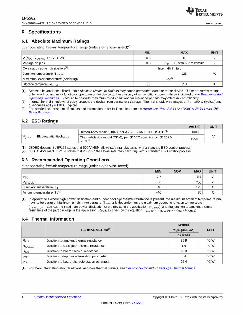
6 Specifications
6.1 Absolute Maximum Ratingsover operating free-air temperature range (unless otherwise noted) (1)
MIN MAX UNITV (VDD, VEN/VCC, R, G, B, W) −0.3 6 VVoltage on pins −0.3 VDD + 0.3 with 6 V maximum VContinuous power dissipation (2) Internally limitedJunction temperature, TJ-MAX 125 °CMaximum lead temperature (soldering) See (3)
Storage temperature, Tstg −65 150 °C
(1) JEDEC document JEP155 states that 500-V HBM allows safe manufacturing with a standard ESD control process.(2) JEDEC document JEP157 states that 250-V CDM allows safe manufacturing with a standard ESD control process.
6.2 ESD RatingsVALUE UNIT
V(ESD) Electrostatic dischargeHuman-body model (HBM), per ANSI/ESDA/JEDEC JS-001 (1) ±1000
VCharged-device model (CDM), per JEDEC specification JESD22-C101 (2) ±250
(1) In applications where high power dissipation and/or poor package thermal resistance is present, the maximum ambient temperature mayhave to be derated. Maximum ambient temperature (TA-MAX) is dependent on the maximum operating junction temperature(TJ-MAX-OP = 125°C), the maximum power dissipation of the device in the application (PD-MAX), and the junction-to ambient thermalresistance of the part/package in the application (RθJA), as given by the equation: TA-MAX = TJ-MAX-OP – (RθJA × PD-MAX).
6.3 Recommended Operating Conditionsover operating free-air temperature range (unless otherwise noted)
MIN NOM MAX UNITVDD 2.7 5.5 VVEN/VCC 1.65 VDD VJunction temperature, TJ −40 125 °CAmbient temperature, TA
(1) −40 85 °C
(1) For more information about traditional and new thermal metrics, see Semiconductor and IC Package Thermal Metrics.
6.4 Thermal Information
THERMAL METRIC (1)LP5562
UNITYQE (DSBGA)12 PINS
RθJA Junction-to-ambient thermal resistance 85.9 °C/WRθJC(top) Junction-to-case (top) thermal resistance 1.0 °C/WRθJB Junction-to-board thermal resistance 15.3 °C/WψJT Junction-to-top characterization parameter 0.6 °C/WψJB Junction-to-board characterization parameter 15.4 °C/W

5
LP5562www.ti.com SNVS820B –APRIL 2013–REVISED DECEMBER 2016
Product Folder Links: LP5562
Submit Documentation FeedbackCopyright © 2013–2016, Texas Instruments Incorporated
(1) The electrical characteristics tables list ensured specifications under the listed recommended conditions except as otherwise modified orspecified by the electrical characteristics test conditions and/or notes. Typical specifications are estimations only and are not verified byproduction testing.
(2) All voltages are with respect to the potential at the GND pins.(3) Minimum and maximum limits are ensured by design, test, or statistical analysis. Typical numbers are not verified by production, but do
represent the most likely norm.(4) Output current accuracy is the difference between the actual value of the output current and programmed value of this current. Matching
is the maximum difference from the average. For the constant current outputs on the part, the following are determined: the maximumoutput current (MAX), the minimum output current (MIN), and the average output current of all outputs (AVG). Two matching numbersare calculated: (MAX – AVG)/AVG and (AVG – MIN)/AVG. The largest number of the two (worst case) is considered the matchingfigure. Note that some manufacturers have different definitions in use.
(5) Saturation voltage is defined as the voltage when the LED current has dropped 10% from the set value.
6.5 Electrical CharacteristicsUnless otherwise specified: limits for typical values are for TA = 25°C and minimum and maximum limits apply over theoperating ambient temperature range (−40°C < TA < +85°C); VIN = 3.6V, VEN/VCC = 1.8 V. (1) (2) (3)
PARAMETER TEST CONDITIONS MIN TYP MAX UNITCURRENT CONSUMPTION AND OSCILLATOR ELECTRICAL CHARACTERISTICS
IVDD
Standby supply current
EN = 0 (pin), CHIP_EN = 0 (bit), external 32kHz clock running or not running 0.2 2 µA
EN = 1 (pin), CHIP_EN = 0 (bit),external 32 kHz clock not running 2 µA
EN = 1 (pin), CHIP_EN = 0 (bit)External 32-kHz clock running 2.4 µA
Normal mode supply currentLED drivers disabled 0.25 mALED drivers enabled 1 mA
Powersave mode supplycurrent
External 32-kHz clock running 10 µAInternal oscillator running 0.25 mA
ƒOSCInternal oscillator frequencyaccuracy
TA = 25°C –4% 4%–7% 7%
LED DRIVER ELECTRICAL CHARACTERISTICS (R, G, B, W OUTPUTS)ILEAKAGE R, G, B, W pin leakage current TA = 25°C 0.1 1 µAIMAX Maximum source current Outputs R, G, B, W 25.5 mA
IOUT Accuracy of output current (4)Output current set to 17.5 mA, VDD = 3.6 VTA = 25°C –4% 4%
Output current set to 17.5 mA, VDD = 3.6 V –5% 5%IMATCH Matching (4) Output current set to 17.5 mA, VDD = 3.6V 1% 2%
ƒLED LED PWM switching frequencyPWM_HF = 1 558
HzPWM_HF = 0 256
VSAT Saturation voltage (5) Output current set to 17.5 mATA = 25°C 60 100 mV

6
LP5562SNVS820B –APRIL 2013–REVISED DECEMBER 2016 www.ti.com
Product Folder Links: LP5562
Submit Documentation Feedback Copyright © 2013–2016, Texas Instruments Incorporated
(1) The I2C host should allow at least 1ms before sending data to the LP5562 after the rising edge of the enable line.
6.6 Logic Interface CharacteristicsUnless otherwise specified: limits for typical values are for TA = 25°C and minimum and maximum limits apply over theoperating ambient temperature range (−40°C < TA < +85°C); VEN = 1.65 V.
PARAMETER TEST CONDITIONS MIN TYP MAX UNITLOGIC INPUT ENVIL Input low level 0.5 VVIH Input high level 1.2 VII Logic input current –1 1 µAtDELAY Input delay (1) 2 µsLOGIC INPUT SCL, SDA, CLK_32K, ADDR_SEL0, ADDR_SEL1, VEN = 1.8 VVIL Input low level 0.2 × VEN VVIH Input high level 0.8 × VEN VII Input current –1 1 µAƒCLK_32K Clock frequency 32 kHzƒSCL Clock frequency 400 kHzLOGIC OUTPUT SDAVOL Output low level IOUT = 3 mA (pullup current) 0.3 0.5 VIL Output leakage current 1 µA
(1) Specification is ensured by design and is not tested in production. VEN = 1.65 V to VDD.(2) The ideal external clock signal for the LP5562 is a 0 V to VEN 25% to 75% duty-cycle square wave. At frequencies above 32.7 kHz,
program execution will be faster and at frequencies below 32.7 kHz program execution will be slower.
6.7 Recommended External Clock Source Conditionsover operating free-air temperature range (unless otherwise noted) (1) (2)
PARAMETER TEST CONDITIONS MIN TYP MAX UNITLOGIC INPUT CLK_32KƒCLK_32K Clock frequency 32.7 kHztCLKH High time 6 µstCLKL Low time 6 µstr Clock rise time 10% to 90% 2 µstf Clock fall time 90% to 10% 2 µs
(1) Specification is ensured by design and is not tested in production. VEN = 1.65 V to VDD.
6.8 I2C Timing Requirements (SDA, SCL)See (1)
MIN MAX UNITƒSCL Clock frequency 400 kHz1 Hold time (repeated) START condition 0.6 µs2 Clock low time 1.3 µs3 Clock high time 600 ns4 Setup time for a repeated START condition 600 ns5 Data hold time 50 ns6 Data setup time 100 ns7 Rise time of SDA and SCL 20 + 0.1Cb 300 ns8 Fall time of SDA and SCL 15 + 0.1Cb 300 ns9 Set-up time for STOP condition 600 ns10 Bus-free time between a STOP and a START condition 1.3 µsCb Capacitive load for each bus line 10 200 pF

SVA-30197402
SVA-30197417
7
LP5562www.ti.com SNVS820B –APRIL 2013–REVISED DECEMBER 2016
Product Folder Links: LP5562
Submit Documentation FeedbackCopyright © 2013–2016, Texas Instruments Incorporated
Figure 1. External Clock Timing
Figure 2. I2C Timing Parameters

0
0.05
0.1
0.15
0.2
0.25
0.3
0.35
0.4
0.45
0.5
0 100 200 300 400 500 600 700
Inpu
t cu
rren
t, m
A
Measurement number
Input current, internal clock,powersave mode, 1 LED
C004
0
0.1
0.2
0.3
0.4
0.5
0 100 200 300 400 500 600 700
Inpi
ut c
urre
nt,
mA
Measurement number
Input current, external clock,powersave, 1 LED
C006
0
0.2
0.4
0.6
0.8
1
1.2
0 100 200 300 400 500 600 700
Inpu
t cu
rren
t, m
A
Measurement number
Input current, internal clock,powersave mode
C003
0
0.2
0.4
0.6
0.8
1
1.2
0 100 200 300 400 500 600 700
Inpu
t cu
rren
t, m
A
Measurement number
Input current, external clock,powersave mode
C002
0
10
20
30
40
50
0 100 200 300 400 500 600 700
Inpu
t cu
rren
t, m
A
Measurement number
Input current, external clock
C001
0
10
20
30
40
50
0 100 200 300 400 500 600 700
Inpu
t cu
rren
t, m
A
Measurement number
Input current, internal clock
C005
8
LP5562SNVS820B –APRIL 2013–REVISED DECEMBER 2016 www.ti.com
Product Folder Links: LP5562
Submit Documentation Feedback Copyright © 2013–2016, Texas Instruments Incorporated
6.9 Typical Characteristics: Current ConsumptionUnless otherwise specified: VDD = 3.6 V, VEN = 3.3 V. Here are presented input current consumption measurements. Currentconsumption is measured during a LED blink program execution. Program code sets every LED output to full PWM value for2 seconds and then PWM is set to 0 for 2 seconds. This is looped endlessly. 750 measurements are taken during onemeasurement cycle.
Figure 3. Input Current Consumption in Normal Mode WithExternal Clock Running. 4 LEDs (RGBW) Set as Load. Every
LED Driver Current Value Is Set to 10 mA.
Figure 4. Input Current Consumption in Normal Mode WithInternal Clock Running. 4 LEDs (RGBW) set as Load. Every
LED Driver Current Value is Set to 10 mA .
Figure 5. Input Current Consumption in Power Save ModeWith External Clock Running, no LEDs as Load. All 4 LED
Drivers are Enabled During Program Execution.
Figure 6. Input Current Consumption in Power Save ModeWith Internal Clock Running, no LEDs as Load. All 4 LED
Drivers are Enabled During Program Execution.
Figure 7. Input Current Consumption in Power Save ModeWith External Clock Running, no LEDs as Load. Only 1 LED
Driver is Enabled During Program Execution.
Figure 8. Input Current Consumption in Power Save ModeWith Internal Clock Running, no LEDs as Load. Only 1 LED
Driver is Enabled During Program Execution.

0
1
2
3
4
5
6
7
8
9
10
0 5 10 15 20 25
Cur
rent
acc
urac
y, %
LED current, mA
WLED RLED
GLED BLED
C010
0
1
2
3
4
5
6
7
0 5 10 15 20 25
LED
cur
rent
mat
chin
g, %
LED current, mA
Matching
C011
0.00
2.00
4.00
6.00
8.00
10.00
12.00
14.00
16.00
18.00
20.00
00.020.040.060.080.10.120.140.160.180.2
LED
cur
rent
, m
A
LED voltage, V
WLED
RLED
GLED
BLED
C008
0.00E+00
5.00E+00
1.00E+01
1.50E+01
2.00E+01
2.50E+01
3.00E+01
0 25 50 75 100 125 150 175 200 225 250
LED
cur
rent
, m
A
Current code
WLED currentRLED currentGLED currentBLED current
C009
0.00E+00
2.00E+00
4.00E+00
6.00E+00
8.00E+00
1.00E+01
1.20E+01
1.40E+01
0 100 200 300 400 500 600 700
Inpu
t cu
rren
t, uA
Measurement number
Input current, external clock,powersave mode, no LEDs
C007
9
LP5562www.ti.com SNVS820B –APRIL 2013–REVISED DECEMBER 2016
Product Folder Links: LP5562
Submit Documentation FeedbackCopyright © 2013–2016, Texas Instruments Incorporated
Typical Characteristics: Current Consumption (continued)Unless otherwise specified: VDD = 3.6 V, VEN = 3.3 V. Here are presented input current consumption measurements. Currentconsumption is measured during a LED blink program execution. Program code sets every LED output to full PWM value for2 seconds and then PWM is set to 0 for 2 seconds. This is looped endlessly. 750 measurements are taken during onemeasurement cycle.
Figure 9. Input Current Consumption in Power Save Mode With External Clock Running, no LEDs as Load and no LED Driversare Enabled During Program Execution.
6.10 Typical Characteristics: LED OutputLED driver typical performance images.
Figure 10. Every LED Driver Saturation Voltage, CurrentSetting 17.5 mA
Figure 11. LED Driver Currents Compared to Current SettingCode
Figure 12. LED Driver Current Accuracy With DifferentCurrent Setting
Figure 13. LED Driver Current Matching Between all LEDDrivers With Different Current Setting

PROGRAM MEMORY
I2C
LP5562
SCL
SDA
CLK_32K
ADDR_SEL0
ADDR_SEL1
EN/VCC
VDD
GND
R
G
B
IDAC
Control
BIAS
REF TSD
POR
OSC
CLK DET
VDD_ IO
Command Based PWM Pattern Generator
1PFCIN
VDD
W
MCU
10
LP5562SNVS820B –APRIL 2013–REVISED DECEMBER 2016 www.ti.com
Product Folder Links: LP5562
Submit Documentation Feedback Copyright © 2013–2016, Texas Instruments Incorporated
7 Detailed Description
7.1 OverviewThe LP5562 is a RGBW LED driver for indicator LED and keypad lighting. The device has an internal programmemory for creating a variety of lighting sequences. When the program memory has been loaded, the LP5562can operate independently without processor control.
The device has 4 LED drivers that are constant current sinks with 8-bit current and 8-bit PWM control. Thecurrent sinks can be controlled via the three execution engines or direct PWM control. The execution engineshave five different functions used to build lighting sequences: Ramp, Set PWM, Go to Start, Branch, or EndTrigger. These control methods and functions are explained in detail in Feature Description and DeviceFunctional Modes.
7.2 Functional Block Diagram
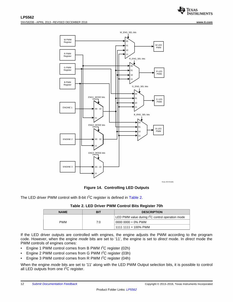
7.3 Feature Description
7.3.1 LED Drivers Operational DescriptionThe LP5562 has 4 LED drivers that are constant current sinks with 8-bit current and 8-bit PWM control. Currentis controlled from I2C registers. PWM can be controlled with program execution engines or direct I2C registerwrites.
7.3.1.1 LED Driver Current ControlLED driver output current can be programmed with I2C register from 0 mA up to 25.5 mA. Current settingresolution is 100 μA (8-bit control).

11
LP5562www.ti.com SNVS820B –APRIL 2013–REVISED DECEMBER 2016
Product Folder Links: LP5562
Submit Documentation FeedbackCopyright © 2013–2016, Texas Instruments Incorporated
Table 1. B_CURRENT Register (05h), G_CURRENT Register (06h), R_CURRENTRegister (07h), W CURRENT Register (0Fh)
NAME BIT DESCRIPTION
CURRENT 7:0
CURRENT SETTINGbin hex dec mA
0000 0000 00 0 0.00000 0001 01 1 0.10000 0010 02 2 0.20000 0011 03 3 0.30000 0100 04 4 0.40000 0101 05 5 0.50000 0110 06 6 0.6
... ... ... ...1010 1111 AF 175 17.5 (def)
... ... ... ...1111 1011 FB 251 25.11111 1100 FC 252 25.21111 1101 FS 253 25.31111 1110 FE 254 25.41111 1111 FF 255 25.5
7.3.1.2 Controlling LED Driver Output PWMPWM can be controlled by either with program execution engines (1, 2 and 3) or via I2C registers (02h for B, 03hfor G, 04h for R and 0Eh for W).
Control of LED driver output PWM selection is managed with 2 bits for each LED output from register 70h. TheTable 3 describes the selection options. With these bits for example all LED outputs can be controlled from oneprogram execution engine.
W PWM Register
R PWM Register
G PWM Register
B PWM Register
ENGINE 1
ENGINE 2
ENGINE 3
W LED PWM
R LED PWM
B LED PWM
G LED PWM
00
01
10
11
W_ENG_SEL bits
00 - 10
11
00 - 10
11
00 - 10
ENG1_MODE bits
ENG2_MODE bits
ENG3_MODE bits
00
01
10
11
00
01
10
11
R_ENG_SEL bits
00
01
10
11
G_ENG_SEL bits
B_ENG_SEL bits
11
SVA-30197406
12
LP5562SNVS820B –APRIL 2013–REVISED DECEMBER 2016 www.ti.com
Product Folder Links: LP5562
Submit Documentation Feedback Copyright © 2013–2016, Texas Instruments Incorporated
Figure 14. Controlling LED Outputs
The LED driver PWM control with 8-bit I2C register is defined in Table 2.
Table 2. LED Driver PWM Control Bits Register 70hNAME BIT DESCRIPTION
PWM 7:0LED PWM value during I2C control operation mode0000 0000 = 0% PWM1111 1111 = 100% PWM
If the LED driver outputs are controlled with engines, the engine adjusts the PWM according to the programcode. However, when the engine mode bits are set to ‘11’, the engine is set to direct mode. In direct mode thePWM controls of engines comes:• Engine 1 PWM control comes from B PWM I2C register (02h)• Engine 2 PWM control comes from G PWM I2C register (03h)• Engine 3 PWM control comes from R PWM I2C register (04h)
When the engine mode bits are set to '11' along with the LED PWM Output selection bits, it is possible to controlall LED outputs from one I2C register.
13
LP5562www.ti.com SNVS820B –APRIL 2013–REVISED DECEMBER 2016
Product Folder Links: LP5562
Submit Documentation FeedbackCopyright © 2013–2016, Texas Instruments Incorporated
Table 3. LED PWM Output Selection BitsB_ENG_SEL bits[1:0]G_ENG_SEL bits[3:2]R_ENG_SEL bits[5:4]W_ENG_SEL bits[7:6]
DESCRIPTION
00 Output is controlled via I2C registers
01 ENG1_MODE and ENG1_EXEC register control LED output PWMinstead of I2C register
10 ENG2_MODE and ENG2_EXEC register control LED output PWMinstead of I2C register
11 ENG3_MODE and ENG3_EXEC register control LED output PWMinstead of I2C register
7.3.2 Direct I2C Register PWM Control Example• Device Start-up
– Supply 3.6 V to VDD– Supply 1.8 V to EN– Wait 1 ms– Write to address 00h 0100 0000b (chip_en to '1')– Wait 500 μs (start-up delay)
• Use internal clock– Write to address 08h 0000 0001b (enable internal clock)
• Direct PWM control– Write to address 70h 0000 0000b (Configure all LED outputs to be controlled from I2C registers)
• Write PWM values– Write to address 02h 1000 0000b (B driver PWM 50% duty cycle)– Write to address 03h 1100 0000b (G driver PWM 75% duty cycle)– Write to address 04h 1111 1111b (R driver PWM 100% duty cycle)
LEDs are turned on after the PWM values are written. Changes to the PWM value registers are reflectedimmediately to the LED brightness. Default LED current (17.5 mA) is used for LED outputs, if no other values arewritten.
PWM frequency is either 256 Hz or 558 Hz. Frequency is set with PWM_HF bit in register 08h. When PWM_HFis 0, the frequency is 256 Hz. When the PWM_HF bit is 1, the PWM frequency is 558 Hz. Brightness adjustmentis either linear or logarithmic. This can be set with LOG_EN bit in register 00h. When LOG_EN = 0 linearadjustment scale is used and when LOG_EN = 1 logarithmic scale is used. By using logarithmic scale the visualeffect seems linear to the eye. Register control bits are presented in following tables:
Table 4. ENABLE Register (00h)NAME BIT DESCRIPTION
LOG_EN 7Logarithmic PWM adjustment enable bit0 = Linear adjustment1 = Logarithmic adjustment
Table 5. CONFIG Register (08h)NAME BIT DESCRIPTION
PWM_HF 6PWM clock frequency0 = 256 Hz1 = 558 Hz

0 25516 32 48 64 80 96 112 128 144 160 176 192 208 224 240
5
10
15
20
25
30
35
40
45
50
55
60
65
70
75
80
85
90
95
100
LOG_EN = 1
LOG_EN = 0
CONTROL (DEC)
BR
IGH
TN
ES
S (
%)
0
SVA-30197405
14
LP5562SNVS820B –APRIL 2013–REVISED DECEMBER 2016 www.ti.com
Product Folder Links: LP5562
Submit Documentation Feedback Copyright © 2013–2016, Texas Instruments Incorporated
Figure 15. Logarithmic and Linear PWM Adjustment Curves
7.3.3 Program Execution EnginesUse of program execution engines is the other LED output PWM control method available in the LP5562. Thedevice has 3 program execution engines. These engines create PWM controlled lighting patterns to the mappedLED outputs according to program codes developed by the user. Program coding is done using programmingcommands (see Program Execution Engine Programming Commands.) Programs are loaded into SRAM memoryand engine control bits are used to run these programs autonomously. LED outputs can be mapped into these 3engines with register 70h bit settings (see Table 3). The engines have different operation modes, programexecution states, and program counters. Each engine has its own section of the SRAM memory.
7.3.3.1 Program Execution Engine StatesEngine program execution is controlled from ENABLE register (00h). There are four different states for eachengine, and these states are described in Table 6.
Table 6. ENABLE Register (00h)NAME BIT DESCRIPTION
ENG1_EXEC 5:4
Engine 1 program execution00b = Hold: Wait until current command is finished then stop whileEXEC mode is hold. PC can be read or written only in this mode.01b = Step: Execute instruction defined by current Engine 1 PC value,increment PC, and change ENG1_EXEC to 00b (Hold).10b = Run: Start at program counter value defined by current Engine 1PC value.11b = Execute instruction defined by current Engine 1 PC value andchange ENG1_EXEC to 00b (Hold).
ENG2_EXEC 3:2
Engine 2 program execution00b = Hold: Wait until current command is finished then stop whileEXEC mode is hold. PC can be read or written only in this mode.01b = Step: Execute instruction defined by current Engine 2 PC value,increment PC, and change ENG2_EXEC to 00b (Hold).10b = Run: Start at program counter value defined by current Engine 2PC value.11b = Execute instruction defined by current Engine 2 PC value andchange ENG2_EXEC to 00b (Hold).
ENG3_EXEC 1:0
Engine 3 program execution00b = Hold: Wait until current command is finished then stop whileEXEC mode is hold. PC can be read or written only in this mode.01b = Step: Execute instruction defined by current engine 3 PC value,increment PC, and change ENG3_EXEC to 00b (Hold).10b = Run: Start at program counter value defined by current engine 3PC value.11b = Execute instruction defined by current engine 3 PC value andchange ENG3_EXEC to 00b (Hold).

15
LP5562www.ti.com SNVS820B –APRIL 2013–REVISED DECEMBER 2016
Product Folder Links: LP5562
Submit Documentation FeedbackCopyright © 2013–2016, Texas Instruments Incorporated
7.3.3.2 Program Execution Engine Operation ModesOperation modes are defined in register address 01h. Each engine (1, 2, 3) operation mode can be configuredseparately. Mode registers are synchronized to a 32-kHz clock. Delay between consecutive I2C writes toOP_MODE register (01h) need to be longer than 153 μs (typ).
Table 7. Operation Mode Register (OP_MODE (01h))NAME BIT DESCRIPTION
ENG1_MODE 5:4
Engine 1 operation mode00b = Disabled, reset engine 1 PC01b = Load program to SRAM, reset engine 1 PC10b = Run program defined by ENG1_EXEC11b = Direct control from B PWM I2C register, reset engine 1 PC
ENG2_MODE 3:2
Engine 2 operation mode00b = Disabled, reset engine 2 PC01b = Load program to SRAM, reset engine 2 PC10b = Run program defined by ENG2_EXEC11b = Direct control from G PWM I2C register, reset engine 2 PC
ENG3_MODE 1:0
Engine 3 operation mode00b = Disabled, reset engine 3 PC01b = Load program to SRAM, reset engine 3 PC10b = Run program defined by ENG3_EXEC11b = Direct control from R PWM I2C register, reset engine 3 PC
7.3.3.2.1 Operation Modes• Disabled
– Each channel can be configured to disabled mode. For the current engine mapped LED output brightnesswill be 0 during this mode. Disabled mode resets respective engine’s PC.
• Load program– LP5562 can store 16 commands for each engine (1, 2, 3). Each command consists of 16 bits. Because
one register has only 8 bits, one command requires two I2C register addresses. In order to reduceprogram load time the LP5562 supports address auto increment. Register address is incremented aftereach 8 data bits. The whole program memory can be written in one I2C write sequence. Program memoryis defined in the LP5562 register table, from address 10h to address 2Fh for engine 1, from address 30hto address 4Fh for engine 2, and from address 50h to address 6Fh for engine 3. In order to accessprogram memory at least one channel operation mode needs to be load program.
– SRAM memory writes are allowed only to the channel in load program mode. All engines are in hold whileone or several engines are in load program mode, and PWM values are frozen for the engines which arenot in load programmode. Program execution continues when all engines are out of load program mode.Load program mode resets respective engine’s Program Counter (PC).
• Run program– Run program mode executes the commands defined in program memory for respective engine (1, 2, 3).
Execution register bits in ENABLE register (00h) define how the program is executed. The program startposition can be programmed to Program Counter register (see Table 8). By manually selecting the PCstart value, user can write different lighting sequences to the SRAM memory, and select appropriatesequence with the PC register. If program counter runs to end (15), next command will be executed fromprogram location 0. If internal clock is used in the run program mode, operation mode needs to be writtendisabled (00b) before disabling the chip (with CHIP_EN bit or EN pin) to ensure that the sequence startsfrom the correct program counter (PC) value when restarting the sequence. PC registers are synchronizedto 32 kHz clock. Delay between consecutive I2C writes to Program Counter (PC) registers (09h, 0Ah, 0Bh)need to be longer than 153μs (typ.).
– Execution registers are synchronized to 32kHz clock. Delay between consecutive I2C writes to ENABLEregister (00h) need to be longer than 488μs (typ.).
– Note that entering LOAD program or Direct Control Mode from RUN PROGRAM mode is not allowed.Engine execution mode should be set to Hold, and Operation Mode to disabled, when changing operationmode from RUN mode.
• Direct control– In Direct control mode the engine PWM output is controlled by R, G and B PWM I2C registers.
16
LP5562SNVS820B –APRIL 2013–REVISED DECEMBER 2016 www.ti.com
Product Folder Links: LP5562
Submit Documentation Feedback Copyright © 2013–2016, Texas Instruments Incorporated
– When engine 1 is in Direct control mode, the engine 1 PWM output is controlled by B PWM I2C register(02h).
– When engine 2 is in Direct control mode, the engine 2 PWM output is controlled by G PWM I2C register(03h).
– When engine 3 is in Direct control mode, the engine 3 PWM output is controlled by R PWM I2C register(04h).
7.3.3.3 Program Execution Engine Program Counter (PC)Program execution engine Program Counter tells the current program code command, which engine is executing.By setting the program counter value before starting the engine execution, user can set the starting point of theprogram execution.
Table 8. Engine1 PC Register (09h), Engine2 PCRegister (0Ah), Engine3 PC Register (0Bh)
NAME BIT DESCRIPTIONPC 3:0 Program counter value from 0 to 15d
7.3.3.4 Program Execution Engine Programming CommandsThe LP5562 has three independent programmable engines (1, 2, 3). Trigger connections between engines arecommon for all engines. All engines have own program memory sections for storing LED lighting patterns.Brightness control and patterns are done with 8-bit PWM control (256 steps) to get accurate and smooth colorcontrol. Program execution is timed with a 32.7-kHz clock. This clock can be generated internally or an external32-kHz clock can be connected to the CLK_32K pin. Using an external clock enables synchronization of LEDtiming to this clock rather than an internal clock. Selection of the clock is made with address 08H bitsINT_CLK_EN and CLK_DET_EN. See External Clock for details. Supported commands are listed in Table 9.

LP5562www.ti.com SNVS820B –APRIL 2013–REVISED DECEMBER 2016
17
Product Folder Links: LP5562
Submit Documentation FeedbackCopyright © 2013–2016, Texas Instruments Incorporated
(1) X means do not care whether 1 or 0.
Table 9. LED Controller Programming Commands (1)
Command 15 14 13 12 11 10 9 8 7 6 5 4 3 2 1 0
RampWait 0 Pre-scale Step time Sign Increment (number of steps)
Set PWM 0 1 0 PWM ValueGo to Start 0 0 0 0 0 0 0 0 0 0 0
Branch 1 0 1 Loop count x Step / command numberEnd 1 1 0 Int Reset X
Trigger 1 1 1 X X X Wait for trigger on engines1, 2, 3 X X X Send trigger to engines 1,2,
3 X

PWM Control Value
Current value
Step time = 31.2 ms
1
2
3
4
5
6
7
8
End of 1st Ramp command, start next command
Steps1 2 43 5 6 7 8 9 10
End of 2nd Ramp command, start next command
Rising ramp, Sign = 0
Downward ramp, Sign = 1
Increment = 4=> 5 cycles
SVA-30197407
18
LP5562SNVS820B –APRIL 2013–REVISED DECEMBER 2016 www.ti.com
Product Folder Links: LP5562
Submit Documentation Feedback Copyright © 2013–2016, Texas Instruments Incorporated
7.3.3.4.1 Ramp/Wait
The ramp command generates a PWM ramp starting from current value. At each ramp step the output isincremented by one. Time for one step is defined with Prescale and Step time bits. Minimum time for one step is0.49 ms and maximum time is 63 × 15.6 ms = 1 second/step, so it is possible to program very fast and also veryslow ramps. Increment value defines how many steps are taken in one command. Number of actual steps isIncrement + 1. Maximum value is 127d, which corresponds to half of full-scale (128 steps). If during rampcommand PWM reaches minimum/maximum (0/255) ramp command will be executed to the end and PWM willstay at minimum/maximum. This enables the ramp command to be used as combined ramp and wait commandin a single instruction.
The ramp command can be used as wait instruction when increment is zero.
Setting register 00h bit LOG_EN sets the scale as either linear to logarithmic. When LOG_EN = 0, linear scale isused, and when LOG_EN = 1, logarithmic scale is used. By using logarithmic scale the visual effect of the rampcommand seems linear to the eye.
Table 10. Ramp/Wait CommandRamp/Wait command
15 14 13 12 11 10 9 8 7 6 5 4 3 2 1 0
0 Pre-scale Step time Sign Increment
Table 11. Ramp/Wait Command BitsNAME VALUE(d) DESCRIPTION
Prescale0 Divides master clock (32.768 Hz) by 16 = 2048 Hz, 0.49 ms cycle time1 Divides master clock (32.768 Hz) by 512 = 64 Hz, 15.6 ms cycle time
Step time 1-63 One ramp increment done in (step time) x (clock after prescale) Note: 0 means set PMWcommand.
Sign0 Increase PWM output1 Decrease PWM output
Increment 0-127 The number of steps is Increment + 1. Note: 0 is a wait instruction.
For example, if following parameters are used for ramp:• Prescale = 1 ≥ cycle time = 15.6 ms• Step time = 2 ≥ time = 15.6 ms × 2 = 31.2 ms• Sign = 0 ≥ rising ramp Increment = 4 ≥ 5 cycles
Ramp command will be: 0100 0010 0000 0100b = 4204h
If current PWM value is 3, and the first command is as described above, the next command is a ramp withotherwise same the parameters, but with Sign = 1 (Command = 4284h), the result will be like in the followingfigure:
Figure 16. Example of 2 Sequential Ramp Commands

19
LP5562www.ti.com SNVS820B –APRIL 2013–REVISED DECEMBER 2016
Product Folder Links: LP5562
Submit Documentation FeedbackCopyright © 2013–2016, Texas Instruments Incorporated
7.3.3.4.2 Set PWM
Set PWM output value from 0 to 255. Command takes sixteen 32-kHz clock cycles (= 488 μs). Setting register00h bit LOG_EN sets the scale from linear to logarithmic.
Table 12. Set PWM Command BitsSet PWM command
15 14 13 12 11 10 9 8 7 6 5 4 3 2 1 00 1 0 0 0 0 0 0 PWM value
7.3.3.4.3 Go-to-Start
Go-to-start command resets the Program Counter register and continues executing program from the 00hlocation. Command takes sixteen 32-kHz clock cycles. Note that default value for all program memory registersis 0000h, which is Go-to-Start command.
Table 13. Go-to-Start Command BitsGo-to-Start command
15 14 13 12 11 10 9 8 7 6 5 4 3 2 1 00 0 0 0 0 0 0 0 0 0 0 0 0 0 0 0
(1) X means do not care whether 1 or 0
7.3.3.4.4 Branch
When branch command is executed, the 'step number' value is loaded to PC, and program execution continuesfrom this location. Looping is done by the number defined in loop count parameter. Nested looping is supported(loop inside loop). The number of nested loops is not limited. Command takes sixteen 32-kHz clock cycles.
Table 14. Branch Command (1)
Branch command15 14 13 12 11 10 9 8 7 6 5 4 3 2 1 01 0 1 Loop count X X X Step number
Table 15. Branch Command BitsNAME VALUE DESCRIPTION
loop count 0-63 The number of loops to be done. 0 means infinite loop.step number 0-15 The step number to be loaded to program counter.
(1) X means do not care whether 1 or 0.
7.3.3.4.5 End
End program execution resets the program counter and sets the corresponding EXEC register to 00b (hold).Command takes sixteen 32 kHz clock cycles.
Table 16. End Command (1)
End command15 14 13 12 11 10 9 8 7 6 5 4 3 2 1 01 1 0 int reset X X X X X X X X X X X
Table 17. End Command BitsNAME VALUE DESCRIPTION
int
0 No interrupt will be sent.
1Send interrupt by setting corresponding status register bit high tonotify that program has ended. Interrupt can only be cleared byreading interrupt status register 0Ch.

20
LP5562SNVS820B –APRIL 2013–REVISED DECEMBER 2016 www.ti.com
Product Folder Links: LP5562
Submit Documentation Feedback Copyright © 2013–2016, Texas Instruments Incorporated
Table 17. End Command Bits (continued)NAME VALUE DESCRIPTION
reset0 Keep the current PWM value.1 Set PWM value to 0.
(1) X means do not care whether 1 or 0.
7.3.3.4.6 Trigger
Wait or send triggers can be used to synchronize operation between different engines. The send-triggercommand takes sixteen 32-kHz clock cycles; the wait-for-trigger command takes at least sixteen 32-kHz clockcycles. The receiving engine stores sent triggers. Received triggers are cleared by wait for trigger command ifreceived triggers match to engines defined in the command. Engine waits until all defined triggers have beenreceived.
Table 18. Trigger Command (1)
15 14 13 12 11 10 9 8 7 6 5 4 3 2 1 01 1 1 X X X wait trigger <2:0> X X X send trigger <2:0> X
ENG3 ENG2 ENG1 ENG3 ENG2 ENG1
Table 19. Trigger Command BitsNAME VALUE(d) DESCRIPTION
waittrigger<2:0> 0-7
Wait for trigger for the engine(s) defined. Several triggers can bedefined in the same command. Bit 0 is engine 1, bit 1 is engine2, bit2 is engine 3.
sendtrigger<2:0> 0-7
Send trigger for the engine(s) defined. Several triggers can bedefined in the same command. Bit 0 is engine 1, bit 1 is engine2, bit2 is engine 3.
7.3.3.5 Program Load and Execution Example• Start up device and configure device to SRAM write mode
– Supply 3.6V to VDD– Supply 1.8V to EN– Wait 1 ms– Generate 32 kHz clock to CLK_32K pin– Write to address 00h 0100 0000b (enable device)– Wait 500 μs (startup delay)– Write to address 01h 0001 0000b (configure engine 1 into 'Load program to SRAM' mode)
• Program load to SRAM– Write to address 10h 0000 0011b (1st ramp command 8MSB)– Write to address 11h 0111 1111b (1st ramp command 8 LSB)– Write to address 12h 0100 1101b (1st wait command 8 MSB)– Write to address 13h 0000 0000b (1st wait command 8 LSB)– Write to address 14h 0000 0011b (2nd ramp command 8 MSB)– Write to address 15h 1111 1111b (2nd ramp command 8 LSB)– Write to address 16h 0110 0000b (2nd wait command 8 MSB)– Write to address 17h 0000 0000b (2nd wait command 8 LSB)
• Enable Power Save and use external 32 kHz clock– Write to address 08h 0010 0000b (enable powersave, use external clock)
• Run program– Write to address 01h 0010 0000b (Configure LED controller operation mode to "Run program" in engine 1)– Write to address 00h 0110 0000b (Configure program execution mode from "Hold" to "Run" in engine 1)
The LP5562 will generate a 1100 ms long LED pattern which will be repeated infinitely. The LED pattern isillustrated in the figure below.
LED PWM mapped to Engine1
PWM value
127
255
Time (ms)
100 200 400300 500 600 700 800 900 1000 1100 1200
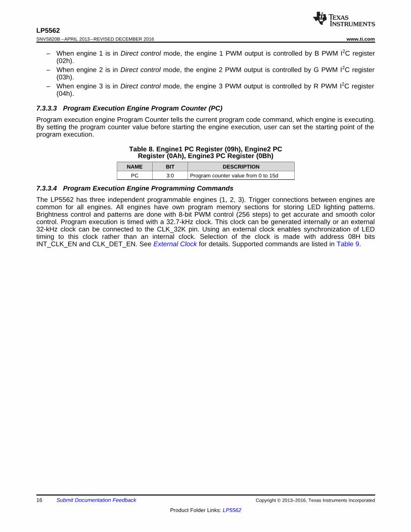
Engine1 program:ramp up to PWM value 128 in 200 mswait 200 msramp down to PWM value 0 in 200 mswait 500 ms
1300 1400 1500 1600 1700
Engine1 program as binary code:0000001101111111010011010000000000000011111111110110000000000000
SVA-30197408
21
LP5562www.ti.com SNVS820B –APRIL 2013–REVISED DECEMBER 2016
Product Folder Links: LP5562
Submit Documentation FeedbackCopyright © 2013–2016, Texas Instruments Incorporated
Figure 17. LED Lighting Pattern and Code for Program Load and Execution Example
7.3.4 Power-Save ModeAutomatic power save mode is enabled when the PS_EN bit in register address 08h is 1. Almost all analogblocks are powered down in power save, if an external clock is used. However, if an internal clock has beenselected, only the LED drivers are disabled during power save since the digital part of the LED controller need toremain active. During program execution the LP5562 can enter power-save mode if there is no PWM activity inengine controlled outputs. To prevent short power-save sequences during program execution, the LP5562 has acommand look-ahead filter. In each instruction cycle every engine commands are analyzed, and if there issufficient time left with no PWM activity, the device will enter power save. In power save program executioncontinues uninterruptedly. When a command that requires PWM activity is executed, fast internal startupsequence will be started automatically. The following tables describe commands and conditions that can activatepower save. All engines need to meet power-save conditions in order to enable power save.
Table 20. Engine Operation Mode and Power SaveENGINE OPERATION
MODE POWER SAVE CONDITION
00b Disabled mode enables power save01b Load program to SRAM mode prevents power save.
10b Run program mode enables power save if there is no PWM activity andcommand look-ahead filter condition is met.
11b Direct control mode enables power save if there is no PWM activity.
Table 21. Engine Commands and Power SaveCOMMAND POWER SAVE CONDITION
Wait No PWM activity and current command wait time longer than 50 ms. Ifprescale = 1 then wait time needs to be longer than 80 ms.
RampRamp command PWM value reaches minimum 0 and current commandexecution time left more than 50 ms. If prescale = 1 then time left needs to bemore than 80 ms.
Trigger No PWM activity during wait for trigger command execution.End No PWM activity or Reset bit = 1.
Set PWM Enables power save if PWM set to 0 and next command generates at least 50ms wait.
Other commands No effect to power save.
22
LP5562SNVS820B –APRIL 2013–REVISED DECEMBER 2016 www.ti.com
Product Folder Links: LP5562
Submit Documentation Feedback Copyright © 2013–2016, Texas Instruments Incorporated
7.3.5 External ClockThe presence of an external clock can be detected by the LP5562. Program execution is clocked with an internal32-kHz clock or with an external clock. Clocking is controlled with register address 08h bits, INT_CLK_EN, andCLK_DET_EN as seen in Table 22.
An external clock can be used if clock is present at the CLK_32K pin. The external clock frequency must be 32kHz for the program execution PWM timing to be as specified. If higher or lower frequency is used, it will affectthe program engine execution speed. If a clock frequency other than 32 kHz is used, the program executiontimings must be scaled accordingly.
The LP5562 has automatic external clock detection. The external clock detector block only detects too low clockfrequency (< 4 kHz), but it is recommended not to use external clock below 20 kHz. If external clock frequency ishigher than specified, the external clock detector notifies that external clock is present. External clock status canbe checked with read only bit EXT_CLK_USED in register address 0Ch, when the external clock detection isenabled (CLK_DET_EN bit = high). If EXT_CLK_USED = 1, then the external clock is detected and it is used fortiming, if automatic clock selection is enabled.
If an external clock is stuck-at-zero or stuck-at-one, or the clock frequency is too low, the clock detector indicatesthat external clock is not present.
If an external clock is not used on the application, CLK_32K pin should be connected to GND to prevent floatingof this pin and extra current consumption.
Table 22. CONFIG Register (08h)NAME BIT DESCRIPTION
CLK_DET_EN,INT_CLK_EN 1:0
LED Controller clock source00b = External clock source (CLK_32K)01b = Internal clock10b = Automatic selection11b = Internal clock
7.3.6 Thermal ShutdownIf the LP5562 reaches thermal shutdown temperature (150°C typical) the device operation is disabled and thedevice state is in STARTUP mode, until no thermal shutdown event is present. Device will enter Normal modewhen temperature drops below 130°C (typical) degrees.
Fault is cleared when thermal shutdown disappears.
7.3.7 Logic Interface Operational DescriptionThe LP5562 features a flexible logic interface for connecting to processor and peripheral devices.Communication is done with the I2C-compatible interface, and different logic input/output pins makes it possibleto synchronize operation of several devices.
7.3.8 I/O LevelsI2C interface, CLK_32K. ADDR_SEL0, and ADDR_SEL1 pins input levels are defined by voltage in EN pin. Usingthe EN pin as a voltage reference for logic inputs simplifies PCB routing and eliminates the need for a dedicatedVIO pin. The following block diagram describes EN pin connections.

InputBuffer
LevelShifter
LevelShifter
SDA
SCL
VDD
EN
LevelShifter
ADDR_SEL0
LevelShifter
ADDR_SEL1
LevelShifter
CLK_32K
SVA-30197409
23
LP5562www.ti.com SNVS820B –APRIL 2013–REVISED DECEMBER 2016
Product Folder Links: LP5562
Submit Documentation FeedbackCopyright © 2013–2016, Texas Instruments Incorporated
Figure 18. Using EN Pin as Digital I/O Voltage Reference
7.3.9 ADDR_SEL0, ADDR_SEL1 PinsThe ADDR_SEL0 and ADDR_SEL1 pins define the device I2C address. Pins are referenced to EN pin signallevel. See I2C Addresses for I2C address definitions.
7.3.10 CLK_32 PinThe CLK_32K pin is used for connecting an external 32-kHz clock to LP5562. An external clock can be used tosynchronize the sequence engines of several LP5562 devices. Using an external clock can also improveautomatic power save mode efficiency, because an internal clock can be switched off automatically when devicehas entered power-save mode, and an external clock is present. Device can be used without the external clock.If external clock is not used on the application, the CLK_32K pin should be connected to GND to prevent floatingof this pin and extra current consumption.
7.4 Device Functional Modes
RESET: In the reset mode all the internal registers are reset to the default values. Reset is done always ifFFh is written to Reset Register (0Dh) or internal Power On Reset is activated. Power On Reset(POR) will activate when supply voltage is connected or when the supply voltage VDD falls below1.5 V (typical). Once VDD rises above 1.9 V (typical), POR will inactivate and the chip will continueto the standby mode. CHIP_EN control bit is low after POR by default.
STANDBY: The standby mode is entered if the register bit CHIP_EN or EN pin is low and Reset is not active.This is the low power consumption mode, when all circuit functions are disabled. Registers can bewritten in this mode if EN pin is high. Control bits are effective after start up.
START-UP: When CHIP_EN bit is written high and EN pin is high, the internal startup sequence powers up allthe needed internal blocks (VREF, Bias, Oscillator etc.). Start-up delay after setting EN pin high is1 ms (typical). Start-up delay after setting chip_en bit to '1' is 500 μs (typical). If the devicetemperature rises too high, the Thermal Shutdown (TSD) disables the device operation and thedevice state is in start-up mode, until no thermal shutdown event is present.
NORMAL: During normal mode the user controls the device using the Control Registers. If EN pin is set low,the CHIP_EN bit is reset to 0.

STANDBY
RESET
INTERNALSTARTUP
SEQUENCE
I2C reset=H and EN=H (pin)
orPOR=H
TSD = H
NORMAL MODE
EN=H (pin) and CHIP_EN=H (bit) EN=L (pin) or
CHIP_EN=L (bit)
POR
TSD = L
POWER SAVE
Enter power save Exit power save
SVA-30197404
24
LP5562SNVS820B –APRIL 2013–REVISED DECEMBER 2016 www.ti.com
Product Folder Links: LP5562
Submit Documentation Feedback Copyright © 2013–2016, Texas Instruments Incorporated
Device Functional Modes (continued)
POWERSAVE:
In power save mode analog blocks are disabled to minimize power consumption. See Power-SaveMode for further information.
Figure 19. Modes of Operation
25
LP5562www.ti.com SNVS820B –APRIL 2013–REVISED DECEMBER 2016
Product Folder Links: LP5562
Submit Documentation FeedbackCopyright © 2013–2016, Texas Instruments Incorporated
7.5 Programming
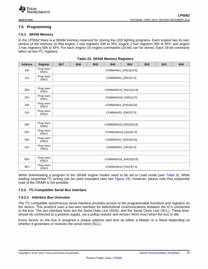
7.5.1 SRAM MemoryIn the LP5562 there is a SRAM memory reserved for storing the LED lighting programs. Each engine has its ownsection of the memory so that engine 1 has registers 10h to 2Fh, engine 2 has registers 30h to 4Fh, and engine3 has registers 50h to 6Fh. For each engine 16 engine commands (16-bit) can be stored. Each 16-bit commandtakes up two I2C registers.
Table 23. SRAM Memory RegistersAddress Register Bit7 Bit6 Bit5 Bit4 Bit3 Bit2 Bit1 Bit0
10h Prog memENG1 COMMAND1_ENG1[15:8]
11h Prog memENG1 COMMAND1_ENG1[7:0]
...
2Eh Prog memENG1 COMMAND16_ENG1[15:8]
2Fh Prog memENG1 COMMAND16_ENG1[7:0]
30h Prog memENG2 COMMAND1_ENG2[15:8]
31h Prog memENG2 COMMAND1_ENG2[7:0]
...
4Eh Prog memENG2 COMMAND16_ENG2[15:8]
4Fh Prog memENG2 COMMAND16_ENG2[7:0]
50h Prog memENG3 COMMAND1_ENG3[15:8]
51h Prog memENG3 COMMAND1_ENG3[7:0]
...
6Eh Prog memENG3 COMMAND16_ENG3[15:8]
6Fh Prog memENG3 COMMAND16_ENG3[7:0]
When downloading a program to the SRAM engine modes need to be set to Load mode (see Table 6). Whileloading sequential I2C writing can be used (repeated start see Figure 24). However, please note that sequentialread of the SRAM is not possible.
7.5.2 I2C-Compatible Serial Bus Interface
7.5.2.1 Interface Bus OverviewThe I2C compatible synchronous serial interface provides access to the programmable functions and registers onthe device. This protocol uses a two-wire interface for bidirectional communications between the IC's connectedto the bus. The two interface lines are the Serial Data Line (SDA), and the Serial Clock Line (SCL). These linesshould be connected to a positive supply, via a pullup resistor and remain HIGH even when the bus is idle.
Every device on the bus is assigned a unique address and acts as either a Master or a Slave depending onwhether it generates or receives the serial clock (SCL).
SDA
SCLS P
START condition STOP condition
SVA-30197412
SC
L
S1 2 3...6 7 8 9
StartCondition
Dat
a O
utpu
tby
Rec
eive
rD
ata
Out
put
by T
rans
mitt
er
Acknowledge Signal from Receiver
Transmitter Stays off theBus During the
Acknowledge Clock
SVA-30197411
SCL
SDA
datachangeallowed
datavalid
datachangeallowed
datavalid
datachangeallowed
SVA-30197410
26
LP5562SNVS820B –APRIL 2013–REVISED DECEMBER 2016 www.ti.com
Product Folder Links: LP5562
Submit Documentation Feedback Copyright © 2013–2016, Texas Instruments Incorporated
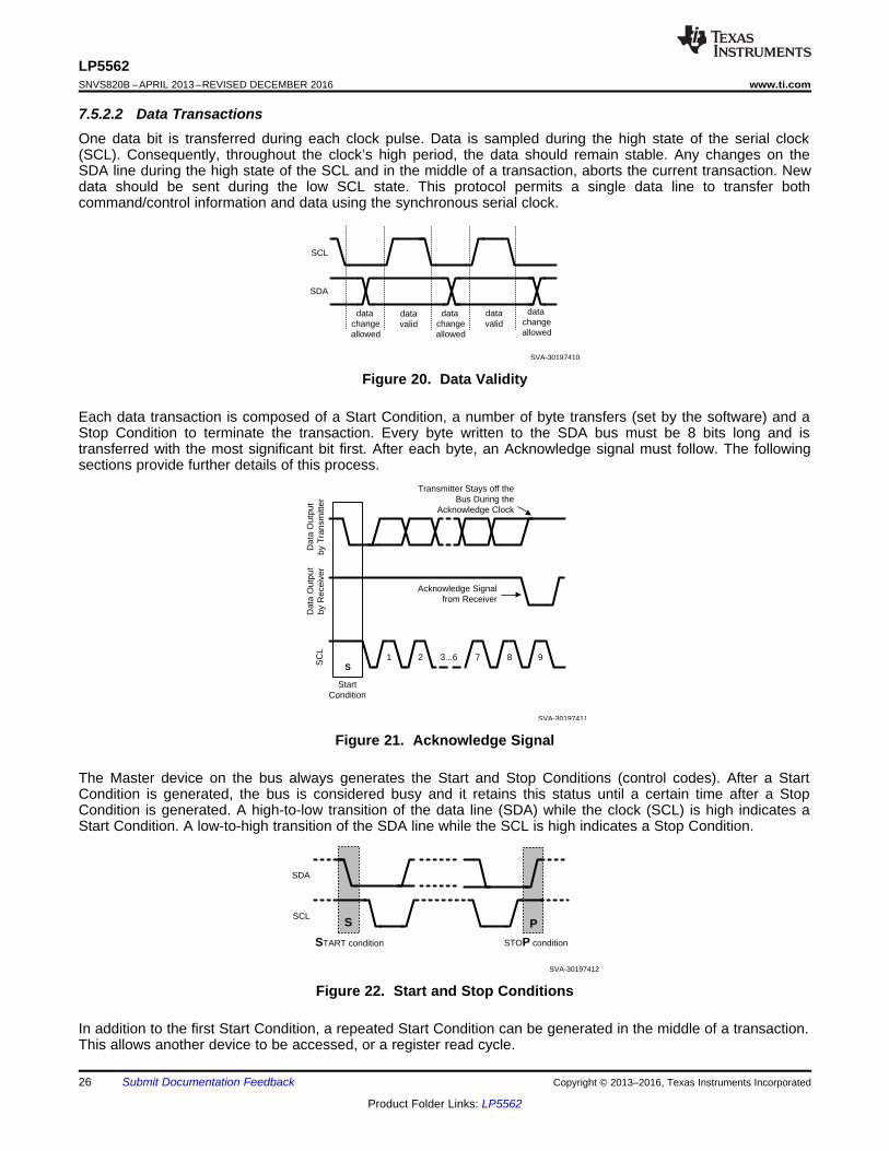
7.5.2.2 Data TransactionsOne data bit is transferred during each clock pulse. Data is sampled during the high state of the serial clock(SCL). Consequently, throughout the clock’s high period, the data should remain stable. Any changes on theSDA line during the high state of the SCL and in the middle of a transaction, aborts the current transaction. Newdata should be sent during the low SCL state. This protocol permits a single data line to transfer bothcommand/control information and data using the synchronous serial clock.
Figure 20. Data Validity
Each data transaction is composed of a Start Condition, a number of byte transfers (set by the software) and aStop Condition to terminate the transaction. Every byte written to the SDA bus must be 8 bits long and istransferred with the most significant bit first. After each byte, an Acknowledge signal must follow. The followingsections provide further details of this process.
Figure 21. Acknowledge Signal
The Master device on the bus always generates the Start and Stop Conditions (control codes). After a StartCondition is generated, the bus is considered busy and it retains this status until a certain time after a StopCondition is generated. A high-to-low transition of the data line (SDA) while the clock (SCL) is high indicates aStart Condition. A low-to-high transition of the SDA line while the SCL is high indicates a Stop Condition.
Figure 22. Start and Stop Conditions
In addition to the first Start Condition, a repeated Start Condition can be generated in the middle of a transaction.This allows another device to be accessed, or a register read cycle.

ADR6Bit7
ADR5bit6
ADR4bit5
ADR3bit4
ADR2bit3
ADR1bit2
ADR0bit1
R/Wbit0
MSB LSB
I2C SLAVE address (chip address)
SVA-30197413
27
LP5562www.ti.com SNVS820B –APRIL 2013–REVISED DECEMBER 2016
Product Folder Links: LP5562
Submit Documentation FeedbackCopyright © 2013–2016, Texas Instruments Incorporated
7.5.2.3 Acknowledge CycleThe Acknowledge Cycle consists of two signals: the acknowledge clock pulse the master sends with each bytetransferred, and the acknowledge signal sent by the receiving device.
The master generates the acknowledge clock pulse on the ninth clock pulse of the byte transfer. The transmitterreleases the SDA line (permits it to go high) to allow the receiver to send the acknowledge signal. The receivermust pull down the SDA line during the acknowledge clock pulse and ensure that SDA remains low during thehigh period of the clock pulse, thus signaling the correct reception of the last data byte and its readiness toreceive the next byte.
7.5.2.4 Acknowledge After Every Byte RuleThe master generates an acknowledge clock pulse after each byte transfer. The receiver sends an acknowledgesignal after every byte received.
There is one exception to the “acknowledge after every byte” rule. When the master is the receiver, it mustindicate to the transmitter an end of data by not-acknowledging (“negative acknowledge”) the last byte clockedout of the slave. This “negative acknowledge” still includes the acknowledge clock pulse (generated by themaster), but the SDA line is not pulled down.
7.5.2.5 Addressing Transfer FormatsEach device on the bus has a unique slave address. The LP5562 operates as a slave device with the 7-bitaddress. LP5562 I2C address is pin selectable from four different choices. If 8-bit address is used forprogramming, the 8th bit is 1 for read and 0 for write. Table 24 shows the 8-bit I2C addresses.
Table 24. I2C AddressesADDR_SEL
[1:0]I 2 C ADDRESS WRITE
(8 bits)I 2 C ADDRESS READ
(8 bits)00 0110 0000 = 60h 0110 0001 = 61h01 0110 0010 = 62h 0110 0011 = 63h10 0110 0100 = 64h 0110 0101 = 65h11 0110 0110 = 66h 0110 0111 = 67h
Before any data is transmitted, the master transmits the address of the slave being addressed.
The slave device should send an acknowledge signal on the SDA line, once it recognizes its address.
The slave address is the first seven bits after a Start Condition. The direction of the data transfer (R/W) dependson the bit sent after the slave address — the eighth bit.
When the slave address is sent, each device in the system compares this slave address with its own. If there is amatch, the device considers itself addressed and sends an acknowledge signal. Depending upon the state of theR/W bit (1:read, 0:write), the device acts as a transmitter or a receiver.
Figure 23. I2C chip address
7.5.2.6 Control Register Write Cycle• Master device generates start condition.• Master device sends slave address (7 bits) and the data direction bit (r/w = 0).• Slave device sends acknowledge signal if the slave address is correct.• Master sends control register address (8 bits).• Slave sends acknowledge signal.• Master sends data byte to be written to the addressed register.

start MSB Chip id LSB w ack MSB Register Addr LSB ack MSB Data LSB ack stop
ack from slave ack from slave ack from slave
SCL
SDA
start id = 011 0000b w ack address = 02H ack ackaddress 02H data stop
SVA-30197414
28
LP5562SNVS820B –APRIL 2013–REVISED DECEMBER 2016 www.ti.com
Product Folder Links: LP5562
Submit Documentation Feedback Copyright © 2013–2016, Texas Instruments Incorporated
• Slave sends acknowledge signal.• If master will send further data bytes the control register address will be incremented by one after
acknowledge signal.• Write cycle ends when the master creates stop condition.
7.5.2.7 Control Register Read Cycle• Master device generates a start condition.• Master device sends slave address (7 bits) and the data direction bit (r/w = 0).• Slave device sends acknowledge signal if the slave address is correct.• Master sends control register address (8 bits).• Slave sends acknowledge signal.• Master device generates repeated start condition.• Master sends the slave address (7 bits) and the data direction bit (r/w = 1).• Slave sends acknowledge signal if the slave address is correct.• Slave sends data byte from addressed register.• If the master device sends acknowledge signal, the control register address will be incremented by one. Slave
device sends data byte from addressed register.• Read cycle ends when the master does not generate acknowledge signal after data byte and generates stop
condition.
(1) <>Data from master [] Data from slave
Table 25. I2C Data Read/Write Flow (1)
ADDRESS MODE
Data Read
<Start Condition><Slave Address><r/w = 0>[Ack]<Register Addr.>[Ack]<Repeated Start Condition><Slave Address><r/w = 1>[Ack][Register Data]<Ack or NAck>... additional reads from subsequent register address possible<Stop Condition>
Data Write
<Start Condition><Slave Address><r/w='0'>[Ack]<Register Addr.>[Ack]<Register Data>[Ack]... additional writes to subsequent register address possible<Stop Condition>
7.5.2.8 Register Read/Write Format
Figure 24. Register Write Format

ack from slave
start MSB Chip id LSB
SCL
ack from slave
w rs r MSB Data LSB stop
ack from slave nack from masterrepeated start data from slave
SDA
start id = 011 0000b w ack address = 00H ack rs r ack address 00H data nack stop
MSB Chip Address LSB
id = 011 0000b
RegisterAddr
MSB LSB
SVA-30197415
29
LP5562www.ti.com SNVS820B –APRIL 2013–REVISED DECEMBER 2016
Product Folder Links: LP5562
Submit Documentation FeedbackCopyright © 2013–2016, Texas Instruments Incorporated
When a read function is to be accomplished, a write function must precede the read function, as show in theRead Cycle waveform.
Figure 25. Register Read Format
w = write (SDA = 0)
r = read (SDA = 1)
ack = acknowledge (SDA pulled down by either master or slave)
rs = repeated start
id = 7-bit chip address

30
LP5562SNVS820B –APRIL 2013–REVISED DECEMBER 2016 www.ti.com
Product Folder Links: LP5562
Submit Documentation Feedback Copyright © 2013–2016, Texas Instruments Incorporated
7.6 Register Maps
Table 26. LP5562 Control Register Names and Default ValuesADDR(HEX) REGISTER D7 D6 D5 D4 D3 D2 D1 D0 DEFAULT
00 ENABLE LOG_EN CHIP_EN ENG1_EXEC[1:0] ENG2_EXEC[1:0] ENG3_EXEC[1:0] 0000 0000
01 OP MODE ENG1_MODE[1:0] ENG2_MODE[1:0] ENG3_MODE[1:0] 0000 0000
02 B PWM B_PWM[7:0] 0000 0000
03 G PWM G_PWM[7:0] 0000 0000
04 R PWM R_PWM[7:0] 0000 0000
05 B CURRENT B_CURRENT[7:0] 1010 1111
06 G CURRENT G_CURRENT[7:0] 1010 1111
07 R CURRENT R_CURRENT[7:0] 1010 1111
08 CONFIG PWM_HF PS_EN CLK_DET_EN INT_CLK_E N 0000 0000
09 ENG1 PC ENG1_PC[3:0] 0000 0000
0A ENG2 PC ENG2_PC[3:0] 0000 0000
0B ENG3 PC ENG3_PC[3:0] 0000 0000
0C STATUS EXT_CLK_USED ENG1_INT ENG2_INT ENG3_INT 0000 0000
0D RESET RESET[7:0] 0000 0000
0E W PWM W_PWM[7:0] 00000000
0F W CURRENT W_CURRENT[7:0] 10101111
70 LED MAP W_ENG_SEL R_ENG_SEL G_ENG_SEL B_ENG_SEL 00111001
10 PROG MEMENG1 CMD_1_ENG1[15:8] 0000 0000
11 PROG MEMENG1 CMD_1_ENG1[7:0] 0000 0000
...
2E PROG MEMENG1 CMD_16_ENG1[15:8] 0000 0000
2F PROG MEMENG1 CMD_16_ENG1[7:0] 0000 0000
30 PROG MEMENG2 CMD_1_ENG2[15:8] 0000 0000
31 PROG MEMENG2 CMD_1_ENG2[7:0] 0000 0000
...
4E PROG MEMENG2 CMD_16_ENG2[15:8] 0000 0000
4F PROG MEMENG2 CMD_16_ENG2[7:0] 0000 0000
50 PROG MEMENG3 CMD_1_ENG3[15:8] 0000 0000
51 PROG MEMENG3 CMD_1_ENG3[7:0] 0000 0000
...
6E PROG MEMENG3 CMD_16_ENG3[15:8] 0000 0000
6F PROG MEMENG3 CMD_16_ENG3[7:0] 0000 0000

31
LP5562www.ti.com SNVS820B –APRIL 2013–REVISED DECEMBER 2016
Product Folder Links: LP5562
Submit Documentation FeedbackCopyright © 2013–2016, Texas Instruments Incorporated
7.6.1 Enable Register (Enable) (Address = 00h) [reset = 00h]EXEC registers are synchronized to the 32-kHz clock. Delay between consecutive I2C writes to ENABLE register(00h) need to be longer than 488 μs (typical).
Figure 26. Enable Register
7 6 5 4 3 2 1 0LOG_EN CHIP_EN ENG1_EXEC[1:0] ENG2_EXEC[1:0] ENG3_EXEC[1:0]
R/W R/W R/W R/W R/WLEGEND: R/W = Read/Write; R = Read only; -n = value after reset
Table 27. Enable Register Field DescriptionsBit Field Type Reset Description7 LOG_EN R/W Logarithmic PWM adjustment generation enable6 CHIP_EN R/W Master chip enable. Enables device internal startup sequence.
See for further information. Setting EN pin low resets theCHIP_EN state to 0. Allow 500 µs delay after setting chip_en bitto '1'
5:4 ENG1_EXEC R/W Engine 1 program execution.00b = Hold: Wait until current command is finished then stopwhile EXEC mode is hold. PC can be read or written only in thismode.01b = Step: Execute instruction defined by current engine 1 PCvalue, increment PC and change ENG1_EXEC to 00b (Hold)10b = Run: Start at program counter value defined by currentengine 1 PC value11b = Execute instruction defined by current engine 1 PC valueand change ENG1_EXEC to 00b (Hold)
3:2 ENG2_EXEC R/W Engine 2 program execution00b = Hold: Wait until current command is finished then stopwhile EXEC mode is hold. PC can be read or written only in thismode.01b = Step: Execute instruction defined by current engine 2 PCvalue, increment PC and change ENG2_EXEC to 00b (Hold)10b = Run: Start at program counter value defined by currentengine 2 PC value11b = Execute instruction defined by current engine 2 PC valueand change ENG2_EXEC to 00b (Hold)
ENG3_EXEC
1:0 R/W Engine 3 program execution00b = Hold: Wait until current command is finished then stopwhile EXEC mode is hold. PC can be read or written only in thismode.01b = Step: Execute instruction defined by current engine 3 PCvalue, increment PC and change ENG3_EXEC to 00b (Hold)10b = Run: Start at program counter value defined by currentengine 3 PC value11b = Execute instruction defined by current engine 3 PC valueand change ENG3_EXEC to 00b (Hold)

32
LP5562SNVS820B –APRIL 2013–REVISED DECEMBER 2016 www.ti.com
Product Folder Links: LP5562
Submit Documentation Feedback Copyright © 2013–2016, Texas Instruments Incorporated
7.6.2 Operation Mode Register (OP Mode) (address = 01h) [reset = 00h]MODE registers are synchronized to 32-kHz clock. Delay between consecutive I2C writes to OP_MODE register(01h) need to be longer than 153 μs (typ).
Figure 27. OP Mode Register
7 6 5 4 3 2 1 0ENG1_MODE[1:0] ENG1_MODE[1:0] ENG1_MODE[1:0]
R/W R/W R/WLEGEND: R/W = Read/Write; R = Read only; -n = value after reset
Table 28. OP Mode Register Field DescriptionsBit Field Type Reset Description5:4 ENG1_MODE R/W Engine 1 operation mode
00b = Disabled01b = Load program to SRAM, reset engine 1 PC10b = Run program defined by ENG1_EXEC11b = Direct control
3:2 ENG2_MODE R/W Engine 2 operation mode00b = Disabled01b = Load program to SRAM, reset engine 2 PC10b = Run program defined by ENG2_EXEC11b = Direct control
1:0 ENG3_MODE R/W Engine 3 operation mode00b = Disabled01b = Load program to SRAM, reset engine 3 PC10b = Run program defined by ENG3_EXEC11b = Direct control
7.6.3 B LED Output PWM Control Register (B_PWM) (address = 02h) [reset = 00h]
Figure 28. B_PWM Control Register
7 6 5 4 3 2 1 0B_PWM[7:0]
R/WLEGEND: R/W = Read/Write; R = Read only; -n = value after reset
Table 29. B_PWM Register Field DescriptionsBit Field Type Reset Description7:0 B_PWM R/W B LED output PWM value during direct control operation mode
33
LP5562www.ti.com SNVS820B –APRIL 2013–REVISED DECEMBER 2016
Product Folder Links: LP5562
Submit Documentation FeedbackCopyright © 2013–2016, Texas Instruments Incorporated
7.6.4 G LED Output PWM Control Register (G_PWM) (address = 03h) [reset = 00h]
Figure 29. G_PWM Control Register
7 6 5 4 3 2 1 0G_PWM[7:0]
R/WLEGEND: R/W = Read/Write; R = Read only; -n = value after reset
Table 30. G_PWM Register Field DescriptionsBit Field Type Reset Description7:0 G_PWM R/W G LED output PWM value during direct control operation mode
7.6.5 R LED Output PWM Control Register (R_PWM) (address = 04h) [reset = 00h]
Figure 30. R_PWM Register
7 6 5 4 3 2 1 0R_PWM[7:0]
R/WLEGEND: R/W = Read/Write; R = Read only; -n = value after reset
Table 31. R_PWM Register Field DescriptionsBit Field Type Reset Description7:0 R_PWM R/W R LED output PWM value during direct control operation mode
7.6.6 B LED Output Current Control Register (B_CURRENT)(address = 05h) [reset = AFh]
Figure 31. B_CURRENT Control Register
7 6 5 4 3 2 1 0B_CURRENT[7:0]
R/WLEGEND: R/W = Read/Write; R = Read only; -n = value after reset
Table 32. B_CURRENT Register Field DescriptionsBit Field Type Reset Description7:0 B_CURRENT R/W Current setting
0000 0000b = 0.0 mA0000 0001b = 0.1 mA0000 0010b = 0.2 mA0000 0011b = 0.3 mA0000 0100b = 0.4 mA0000 0101b = 0.5 mA0000 0110b = 0.6 mA...1010 1111b = 17.5 mA (default)...1111 1011b = 25.1 mA1111 1100b = 25.2 mA1111 1101b = 25.3 mA1111 1110b = 25.4 mA1111 1111b = 25.5 mA

34
LP5562SNVS820B –APRIL 2013–REVISED DECEMBER 2016 www.ti.com
Product Folder Links: LP5562
Submit Documentation Feedback Copyright © 2013–2016, Texas Instruments Incorporated
7.6.7 G LED Output Current Control Register (G_CURRENT)(address = 06h) [reset = AFh]
Figure 32. G_CURRENT Control Register
7 6 5 4 3 2 1 0G_CURRENT[7:0]
R/WLEGEND: R/W = Read/Write; R = Read only; -n = value after reset
Table 33. G_CURRENT Register Field DescriptionsBit Field Type Reset Description7:0 G_CURRENT R/W Current setting
0000 0000b = 0.0 mA0000 0001b = 0.1 mA0000 0010b = 0.2 mA0000 0011b = 0.3 mA0000 0100b = 0.4 mA0000 0101b = 0.5 mA0000 0110b = 0.6 mA...1010 1111b = 17.5 mA (default)...1111 1011b = 25.1 mA1111 1100b = 25.2 mA1111 1101b = 25.3 mA1111 1110b = 25.4 mA1111 1111b = 25.5 mA

35
LP5562www.ti.com SNVS820B –APRIL 2013–REVISED DECEMBER 2016
Product Folder Links: LP5562
Submit Documentation FeedbackCopyright © 2013–2016, Texas Instruments Incorporated
7.6.8 R LED Output Current Control Register (R_CURRENT) (address = 07h) [reset = AFh]
Figure 33. R_CURRENT Control Register
7 6 5 4 3 2 1 0R_CURRENT[7:0]
R/WLEGEND: R/W = Read/Write; R = Read only; -n = value after reset
Table 34. R_CURRENT Register Field DescriptionsBit Field Type Reset Description7:0 R_CURRENT R/W Current setting
0000 0000b = 0.0 mA0000 0001b = 0.1 mA0000 0010b = 0.2 mA0000 0011b = 0.3 mA0000 0100b = 0.4 mA0000 0101b = 0.5 mA0000 0110b = 0.6 mA...1010 1111b = 17.5 mA (default)...1111 1011b = 25.1 mA1111 1100b = 25.2 mA1111 1101b = 25.3 mA1111 1110b = 25.4 mA1111 1111b = 25.5 mA
7.6.9 Configuration Control Register (CONFIG) (address = 08h) [reset = 00h]
Figure 34. CONFIG Register
7 6 5 4 3 2 1 0PWM_HF PS_EN CLK_DET_EN INT_CLK_EN
R/W R/W R/W R/WLEGEND: R/W = Read/Write; R = Read only; -n = value after reset
Table 35. CONFIG Register Field DescriptionsBit Field Type Reset Description6 PWM_HF R/W PWM clock
0 = 256-Hz PWM clock used1 = 558-Hz PWM clock used
5 PWRSAVE_EN R/W Power save mode enable1:0 CLK_DET_EN,
INT_CLK_ENR/W LED Controller clock source
00b = External clock source (CLK_32K)01b = Internal clock10b = Automatic selection11b = Internal clock
36
LP5562SNVS820B –APRIL 2013–REVISED DECEMBER 2016 www.ti.com
Product Folder Links: LP5562
Submit Documentation Feedback Copyright © 2013–2016, Texas Instruments Incorporated
7.6.10 Engine 1 Program Counter Value Register (Engine 1 PC) (address = 09h) [reset = 00h]PC registers are synchronized to a 32-kHz clock. Delay between consecutive I2C writes to PC registers needs tobe longer than 153 μs (typical). PC register can be read or written only when EXEC mode is hold.
Figure 35. Engine 1 PC Value Register
7 6 5 4 3 2 1 0ENG1_PC[3:0]
R/WLEGEND: R/W = Read/Write; R = Read only; -n = value after reset
Table 36. Engine 1 PC Register Field DescriptionsBit Field Type Reset Description3:0 ENG1_PC R/W Engine 1 program counter value
7.6.11 Engine 2 Program Counter Value Register (Engine 2 PC) (address = 0Ah) [reset = 00h]PC registers are synchronized to 32-kHz clock. Delay between consecutive I2C writes to PC registers needs tobe longer than 153 μs (typical). PC register can be read or written only when EXEC mode is hold.
Figure 36. Engine 2 PC Value Register
7 6 5 4 3 2 1 0ENG2_PC[3:0]
R/WLEGEND: R/W = Read/Write; R = Read only; -n = value after reset
Table 37. Engine 2 PC Register Field DescriptionsBit Field Type Reset Description3:0 ENG2_PC R/W Engine 2 program counter value
7.6.12 Engine 3 Program Counter Value Register (Engine 3 PC) (address = 0Ah) [reset = 00h]PC registers are synchronized to 32 kHz clock. Delay between consecutive I2C writes to PC registers needs tobe longer than 153 μs (typ.). PC register can be read or written only when EXEC mode is hold.
Figure 37. Engine 3 PC Value Register
7 6 5 4 3 2 1 0ENG3_PC[3:0]
R/WLEGEND: R/W = Read/Write; R = Read only; -n = value after reset
Table 38. Engine 3 PC Register Field DescriptionsBit Field Type Reset Description3:0 ENG3_PC R/W Engine 3 program counter value

37
LP5562www.ti.com SNVS820B –APRIL 2013–REVISED DECEMBER 2016
Product Folder Links: LP5562
Submit Documentation FeedbackCopyright © 2013–2016, Texas Instruments Incorporated
7.6.13 STATUS/INTERRUPT Register (address = 0Ch) [reset = 00h]Note:Register INT bits will be cleared when read operation to Status/Interrupt register occurs.
Figure 38. STATUS/INTERRUPT Register
7 6 5 4 3 2 1 0EXT_CLK
USEDENG1_INT ENG2_INT ENG3_INT
R R R RLEGEND: R/W = Read/Write; R = Read only; -n = value after reset
Table 39. STATUS/INTERRUPT Register Field DescriptionsBit Field Type Reset Description3 EXT_CLK USED R External clock state
0 = Internal clock used1 = External 32kHz clock used
2 ENG1_INT R Interrupt from engine 11 ENG2_INT R Interrupt from engine 20 ENG3_INT R Interrupt from engine 3
7.6.14 RESET Register (address = 0Dh) [reset = 00h]
Figure 39. RESET Register
7 6 5 4 3 2 1 0RESET[7:0]
R/WLEGEND: R/W = Read/Write; R = Read only; -n = value after reset
Table 40. RESET Register Field DescriptionsBit Field Type Reset Description7:0 RESET R/W Reset all register values when FFh is written.
7.6.15 WLED Output PWM Control Register (W_PWM) (address = 0Eh) [reset = 00h]
Figure 40. W_PWM Control Register
7 6 5 4 3 2 1 0W_PWM[7:0]
R/WLEGEND: R/W = Read/Write; R = Read only; -n = value after reset
Table 41. W_PWM Register Field DescriptionsBit Field Type Reset Description7:0 W_PWM R/W W LED Output PWM value during direct control operation mode
38
LP5562SNVS820B –APRIL 2013–REVISED DECEMBER 2016 www.ti.com
Product Folder Links: LP5562
Submit Documentation Feedback Copyright © 2013–2016, Texas Instruments Incorporated
7.6.16 W LED Output Current Control Register (W_CURRENT) (address = 0Fh) [reset = AFh]
Figure 41. W_CURRENT Control Register
7 6 5 4 3 2 1 0W_CURRENT[7:0]
R/WLEGEND: R/W = Read/Write; R = Read only; -n = value after reset
Table 42. W_CURRENT Register Field DescriptionsBit Field Type Reset Description7:0 W_CURRENT R/W Current setting
0000 0000b = 0.0 mA0000 0001b = 0.1 mA0000 0010b = 0.2 mA0000 0011b = 0.3 mA0000 0100b = 0.4 mA0000 0101b = 0.5 mA0000 0110b = 0.6 mA...1010 1111b = 17.5 mA (default)... 1111 1011b = 25.1 mA1111 1100b = 25.2 mA1111 1101b = 25.3 mA1111 1110b = 25.4 mA1111 1111b = 25.5 mA
7.6.17 LED Mapping Register (LED Map) (address = 70h) [reset = 39h]
Figure 42. LED Map Register
7 6 5 4 3 2 1 0W_ENG_SEL[1:0] R_ENG_SEL[1:0] G_ENG_SEL[1:0] B_ENG_SEL[1:0]
R/W R/W R/W R/WLEGEND: R/W = Read/Write; R = Read only; -n = value after reset
Table 43. LED Map Register Field DescriptionsBit Field Type Reset Description7:6 W_ENG_SEL R/W Selection from where W LED output PWM is controlled, 00 = I2C
register 0Eh, 01 = Engine 1, 10 = Engine 2, 11 = Engine 35:4 R_ENG_SEL R/W Selection from where R LED output PWM is controlled 00 = I2C
register 04h, 01 = Engine 1, 10 = Engine 2, 11 = Engine 33:2 G_ENG_SEL R/W Selection from where G LED output PWM is controlled 00 = I2C
register 03h, 01 = Engine 1, 10 = Engine 2, 11 = Engine 31:0 B_ENG_SEL R/W Selection from where B LED output PWM is controlled 00 = I2C
register 02h, 01 = Engine 1, 10 = Engine 2, 11 = Engine 3

39
LP5562www.ti.com SNVS820B –APRIL 2013–REVISED DECEMBER 2016
Product Folder Links: LP5562
Submit Documentation FeedbackCopyright © 2013–2016, Texas Instruments Incorporated
7.6.18 Program Memory (address = 10h – 6Fh) [reset = 00h]See chapter SRAM Memory for further information.
Figure 43. Program Execution Engine Commands
Command 15 14 13 12 11 10 9 8 7 6 5 4 3 2 1 0RampWait 0 Pre-
scaleStep time Sign Increment
Set PWM 0 1 0 PWM ValueGo toStart 0 0 0 0 0 0 0 0 0 0 0
Branch 1 0 1 Loop Count X Step numberEnd 1 1 0 Int Reset X
Trigger 1 1 1 Wait for trigger on channels 5-0 Send trigger on channels 5-0 XLEGEND: R/W = Read/Write; R = Read only; -n = value after reset

LP5562MCU
1 PFCIN
SCL
SDA
CLK_32K
ADDR_SEL0
ADDR_SEL1
EN/VCC
VDD
GND
R
G
B-
+
RGB LED 0...25.5 mA/LED
WLED
VDD
40
LP5562SNVS820B –APRIL 2013–REVISED DECEMBER 2016 www.ti.com
Product Folder Links: LP5562
Submit Documentation Feedback Copyright © 2013–2016, Texas Instruments Incorporated
8 Application and Implementation
NOTEInformation in the following applications sections is not part of the TI componentspecification, and TI does not warrant its accuracy or completeness. TI’s customers areresponsible for determining suitability of components for their purposes. Customers shouldvalidate and test their design implementation to confirm system functionality.
8.1 Application InformationThe LP5562 is designed for mobile applications with an input voltage VIN between 2.7 V to 5.5 V to support a 1Slithium-ion battery source. A microcontroller or other I2C host is required to initialize and configure the LP5562after power-up. An internal of external 32-kHz clock is required. If multiple LP5562 devices are used to sequencemultiple RGB LEDs, then the external 32-kHz clock input is required. The ADDRSEL0 and ADDRSEL1 pins canbe used to allow unique sequencing of up to four LP5562 devices on the same I2C bus.
The four LED current drivers can be configured up to 25.5-mA LED current each and are tolerant up to 6-V LEDsupply voltage.
8.2 Typical ApplicationFigure 44 shows the typical application for LP5562 supporting one RGB LED and one White LED with the fourLED current outputs.
Figure 44. LP5562 Typical Application
8.2.1 Design RequirementsFor typical LED-driver applications, use the parameters listed in Table 44.
Table 44. Design ParametersDESIGN PARAMETER EXAMPLE VALUEMinimum input voltage 2.7 VMaximum input voltage 5.5 V
EN/VCC logic level 1.8 VR output current 24 mAG output current 20 mAB output current 22 mA
WLED output current 18 mAPWM frequency 256 Hz
32-kHz clock source ExternalLight engines 1, 2 and 3 Blink on/off
Power-save mode Enabled

41
LP5562www.ti.com SNVS820B –APRIL 2013–REVISED DECEMBER 2016
Product Folder Links: LP5562
Submit Documentation FeedbackCopyright © 2013–2016, Texas Instruments Incorporated
8.2.2 Detailed Design Procedure
Table 45. Recommended External ComponentsMODEL TYPE VENDOR VOLTAGE RATING SIZE INCH (MM)
1 µF for CIN
C1005X5R1A105K Ceramic X5R TDK 10 V 0402 (1005)GRM155R61A105KE15D Ceramic X5R Murata 10 V 0402 (1005)LEDs User Defined
8.2.2.1 Output Current Configuration• For 22-mA “B” output current the register address 0x05 is set to 0xDC. B_CURRENT[7:0] = (22 mA / 0.1) =
220 decimal.• For 22-mA “G” output current the register address 0x06 is set to 0xC8. G_CURRENT[7:0] = (20 mA / 0.1) =
200 decimal.• For 24-mA “R” output current the register address 0x07 is set to 0xF0. R_CURRENT[7:0] = (24 mA / 0.1) =
240 decimal.• For 18-mA “WLED” output current the register address 0x0F is set to 0xB4. W_CURRENT[7:0] = (18 mA /
0.1) = 180 decimal.
8.2.2.2 PWM Frequency ConfigurationTo set the PWM frequency to 256 Hz the PWM_HF bit must be written to '0'. It is located at register address0x08 bit 6.
8.2.2.3 Clock Source ConfigurationTo set the clock source to external clock input the INT_CLK_EN and CLK_DET_EN bits are set to “00”. Theseare located at register address 0x08 bits 0 and 1.
8.2.2.4 Power-Save Mode ConfigurationTo enable the power save mode function the PWRSAVE_EN bit must be set to '1'. It is located at registeraddress 0x08 bit 5.

42
LP5562SNVS820B –APRIL 2013–REVISED DECEMBER 2016 www.ti.com
Product Folder Links: LP5562
Submit Documentation Feedback Copyright © 2013–2016, Texas Instruments Incorporated
8.2.2.5 Light Engine ConfigurationSample code for 100% to 0% duty blinking LED function is shown in Table 46.
Table 46. LED Function Sample CodesADDRESS VALUE COMMENTSEngine 1 Section Start
0 40FF
Loop1
set_pwm 2551 4D00 wait 2002 4000 set_pwm 03 6000 wait 5004 A200 branch 4, loop15 D000 end, i
Engine 2 Section Start10 40FF
Loop2
set_pwm 25511 4D00 wait 20012 4000 set_pwm 013 6000 wait 50014 A290 branch 5, loop215 D000 end, i
Engine 3 Section Start20 40FF
Loop3
set_pwm 25521 4D00 wait 20022 4000 set_pwm 023 6000 wait 50024 A320 branch 6, loop325 D000 end, i
8.2.3 Application Curve
External Clock PS. Blink-Program
Figure 45. LED Driver Current Accuracy vs RGBW Current

W VDDCLK32K
B
ADDRSEL1
ADDRSEL0
GND G
SDA SCLEN/VCC
R
TO HOST
TO HOST
TO HOST
TO HOST
BLUE
GREEN
RED
WHITE
VDD
GND
43
LP5562www.ti.com SNVS820B –APRIL 2013–REVISED DECEMBER 2016
Product Folder Links: LP5562
Submit Documentation FeedbackCopyright © 2013–2016, Texas Instruments Incorporated
9 Power Supply RecommendationThe LP5562 is intended to operate from a single cell lithium-ion battery or battery charger up to 5.5 V. Theresistance of the input supply rail should be low enough so that the input current transient does not cause toohigh drop at the LP5562 VDD pin. If the input supply is also powering the LEDs and is connected by using longwires additional bulk capacitance may be required in addition to the ceramic bypass capacitors in the VDD / LEDsupply line.
10 Layout
10.1 Layout GuidelinesFigure 46 is a layout recommendation for the LP5562 used to demonstrate the principles of good layout. Thisexample is for a 2-layer PCB and a single LP5562 device. This layout can be adapted to the actual applicationlayout if/where possible. If multiple LP5562 devices are used in the application then not all the ADDRSEL pinswill be tied to ground. In that case a PCB using HDI process is needed to route ADDRSEL0 and GND bumps.The VDD decoupling cap must be placed close to VDD bump, and the traces for W, R, G, and B bumps must besized to carry 25.5 mA.
10.2 Layout Example
Figure 46. LP5562 Layout Example

44
LP5562SNVS820B –APRIL 2013–REVISED DECEMBER 2016 www.ti.com
Product Folder Links: LP5562
Submit Documentation Feedback Copyright © 2013–2016, Texas Instruments Incorporated
11 Device and Documentation Support
11.1 Device Support
11.1.1 Third-Party Products DisclaimerTI'S PUBLICATION OF INFORMATION REGARDING THIRD-PARTY PRODUCTS OR SERVICES DOES NOTCONSTITUTE AN ENDORSEMENT REGARDING THE SUITABILITY OF SUCH PRODUCTS OR SERVICESOR A WARRANTY, REPRESENTATION OR ENDORSEMENT OF SUCH PRODUCTS OR SERVICES, EITHERALONE OR IN COMBINATION WITH ANY TI PRODUCT OR SERVICE.
11.2 Documentation Support
11.2.1 Related DocumentationFor additional information, see the following:
AN-1112 DSBGA Wafer Level Chip Scale Package.
11.3 Community ResourcesThe following links connect to TI community resources. Linked contents are provided "AS IS" by the respectivecontributors. They do not constitute TI specifications and do not necessarily reflect TI's views; see TI's Terms ofUse.
TI E2E™ Online Community TI's Engineer-to-Engineer (E2E) Community. Created to foster collaborationamong engineers. At e2e.ti.com, you can ask questions, share knowledge, explore ideas and helpsolve problems with fellow engineers.
Design Support TI's Design Support Quickly find helpful E2E forums along with design support tools andcontact information for technical support.
11.4 TrademarksE2E is a trademark of Texas Instruments.All other trademarks are the property of their respective owners.
11.5 Electrostatic Discharge CautionThis integrated circuit can be damaged by ESD. Texas Instruments recommends that all integrated circuits be handled withappropriate precautions. Failure to observe proper handling and installation procedures can cause damage.
ESD damage can range from subtle performance degradation to complete device failure. Precision integrated circuits may be moresusceptible to damage because very small parametric changes could cause the device not to meet its published specifications.
11.6 GlossarySLYZ022 — TI Glossary.
This glossary lists and explains terms, acronyms, and definitions.
12 Mechanical, Packaging, and Orderable InformationThe following pages include mechanical, packaging, and orderable information. This information is the mostcurrent data available for the designated devices. This data is subject to change without notice and revision ofthis document. For browser-based versions of this data sheet, refer to the left-hand navigation.
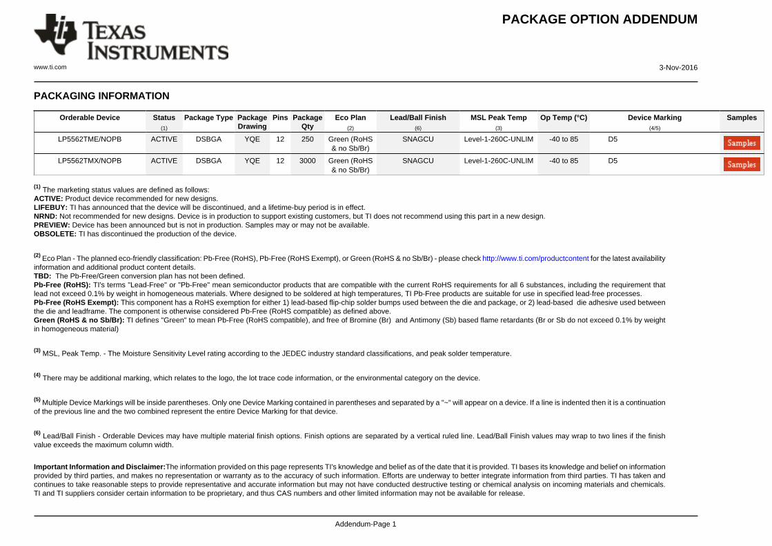
PACKAGE OPTION ADDENDUM
www.ti.com 3-Nov-2016
Addendum-Page 1
PACKAGING INFORMATION
Orderable Device Status(1)
Package Type PackageDrawing
Pins PackageQty
Eco Plan(2)
Lead/Ball Finish(6)
MSL Peak Temp(3)
Op Temp (°C) Device Marking(4/5)
Samples
LP5562TME/NOPB ACTIVE DSBGA YQE 12 250 Green (RoHS& no Sb/Br)
SNAGCU Level-1-260C-UNLIM -40 to 85 D5
LP5562TMX/NOPB ACTIVE DSBGA YQE 12 3000 Green (RoHS& no Sb/Br)
SNAGCU Level-1-260C-UNLIM -40 to 85 D5
(1) The marketing status values are defined as follows:ACTIVE: Product device recommended for new designs.LIFEBUY: TI has announced that the device will be discontinued, and a lifetime-buy period is in effect.NRND: Not recommended for new designs. Device is in production to support existing customers, but TI does not recommend using this part in a new design.PREVIEW: Device has been announced but is not in production. Samples may or may not be available.OBSOLETE: TI has discontinued the production of the device.
(2) Eco Plan - The planned eco-friendly classification: Pb-Free (RoHS), Pb-Free (RoHS Exempt), or Green (RoHS & no Sb/Br) - please check http://www.ti.com/productcontent for the latest availabilityinformation and additional product content details.TBD: The Pb-Free/Green conversion plan has not been defined.Pb-Free (RoHS): TI's terms "Lead-Free" or "Pb-Free" mean semiconductor products that are compatible with the current RoHS requirements for all 6 substances, including the requirement thatlead not exceed 0.1% by weight in homogeneous materials. Where designed to be soldered at high temperatures, TI Pb-Free products are suitable for use in specified lead-free processes.Pb-Free (RoHS Exempt): This component has a RoHS exemption for either 1) lead-based flip-chip solder bumps used between the die and package, or 2) lead-based die adhesive used betweenthe die and leadframe. The component is otherwise considered Pb-Free (RoHS compatible) as defined above.Green (RoHS & no Sb/Br): TI defines "Green" to mean Pb-Free (RoHS compatible), and free of Bromine (Br) and Antimony (Sb) based flame retardants (Br or Sb do not exceed 0.1% by weightin homogeneous material)
(3) MSL, Peak Temp. - The Moisture Sensitivity Level rating according to the JEDEC industry standard classifications, and peak solder temperature.
(4) There may be additional marking, which relates to the logo, the lot trace code information, or the environmental category on the device.
(5) Multiple Device Markings will be inside parentheses. Only one Device Marking contained in parentheses and separated by a "~" will appear on a device. If a line is indented then it is a continuationof the previous line and the two combined represent the entire Device Marking for that device.
(6) Lead/Ball Finish - Orderable Devices may have multiple material finish options. Finish options are separated by a vertical ruled line. Lead/Ball Finish values may wrap to two lines if the finishvalue exceeds the maximum column width.
Important Information and Disclaimer:The information provided on this page represents TI's knowledge and belief as of the date that it is provided. TI bases its knowledge and belief on informationprovided by third parties, and makes no representation or warranty as to the accuracy of such information. Efforts are underway to better integrate information from third parties. TI has taken andcontinues to take reasonable steps to provide representative and accurate information but may not have conducted destructive testing or chemical analysis on incoming materials and chemicals.TI and TI suppliers consider certain information to be proprietary, and thus CAS numbers and other limited information may not be available for release.

PACKAGE OPTION ADDENDUM
www.ti.com 3-Nov-2016
Addendum-Page 2
In no event shall TI's liability arising out of such information exceed the total purchase price of the TI part(s) at issue in this document sold by TI to Customer on an annual basis.

TAPE AND REEL INFORMATION
*All dimensions are nominal
Device PackageType
PackageDrawing
Pins SPQ ReelDiameter
(mm)
ReelWidth
W1 (mm)
A0(mm)
B0(mm)
K0(mm)
P1(mm)
W(mm)
Pin1Quadrant
LP5562TME/NOPB DSBGA YQE 12 250 178.0 8.4 1.35 1.75 0.76 4.0 8.0 Q2
LP5562TMX/NOPB DSBGA YQE 12 3000 178.0 8.4 1.35 1.75 0.76 4.0 8.0 Q2
PACKAGE MATERIALS INFORMATION
www.ti.com 3-Nov-2016
Pack Materials-Page 1

*All dimensions are nominal
Device Package Type Package Drawing Pins SPQ Length (mm) Width (mm) Height (mm)
LP5562TME/NOPB DSBGA YQE 12 250 210.0 185.0 35.0
LP5562TMX/NOPB DSBGA YQE 12 3000 210.0 185.0 35.0
PACKAGE MATERIALS INFORMATION
www.ti.com 3-Nov-2016
Pack Materials-Page 2
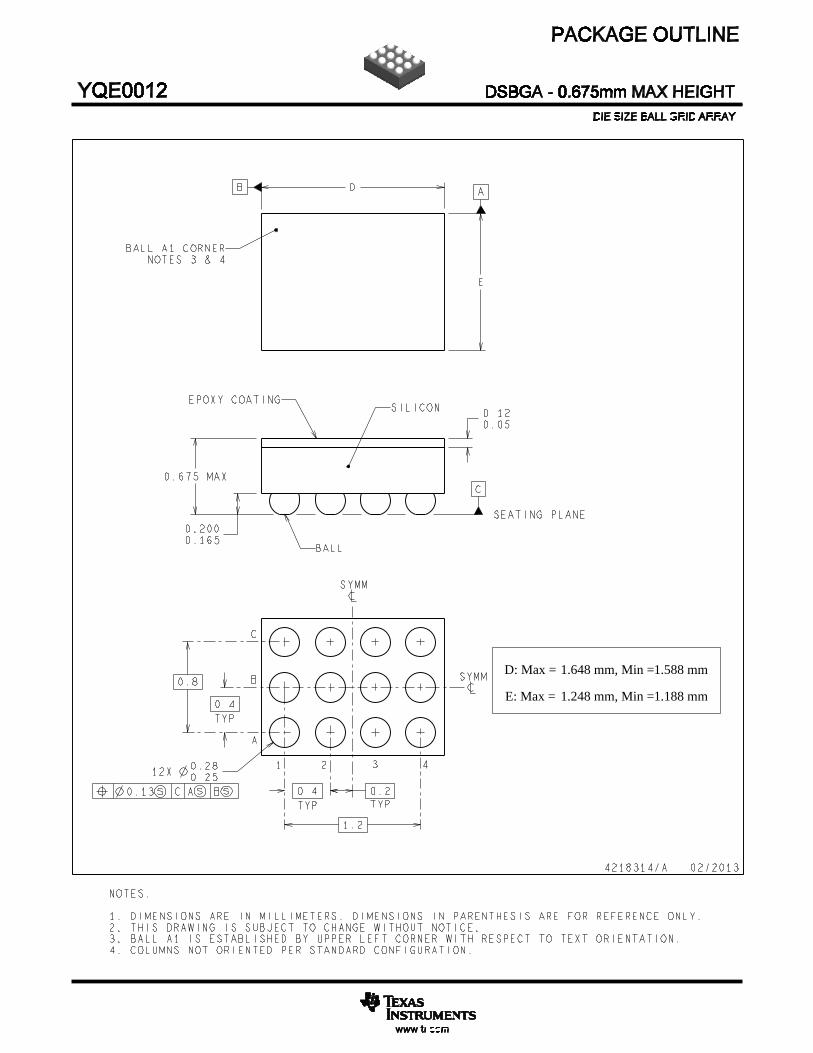
D: Max =
E: Max =
1.648 mm, Min =
1.248 mm, Min =
1.588 mm
1.188 mm


IMPORTANT NOTICE
Texas Instruments Incorporated (TI) reserves the right to make corrections, enhancements, improvements and other changes to itssemiconductor products and services per JESD46, latest issue, and to discontinue any product or service per JESD48, latest issue. Buyersshould obtain the latest relevant information before placing orders and should verify that such information is current and complete.TI’s published terms of sale for semiconductor products (http://www.ti.com/sc/docs/stdterms.htm) apply to the sale of packaged integratedcircuit products that TI has qualified and released to market. Additional terms may apply to the use or sale of other types of TI products andservices.Reproduction of significant portions of TI information in TI data sheets is permissible only if reproduction is without alteration and isaccompanied by all associated warranties, conditions, limitations, and notices. TI is not responsible or liable for such reproduceddocumentation. Information of third parties may be subject to additional restrictions. Resale of TI products or services with statementsdifferent from or beyond the parameters stated by TI for that product or service voids all express and any implied warranties for theassociated TI product or service and is an unfair and deceptive business practice. TI is not responsible or liable for any such statements.Buyers and others who are developing systems that incorporate TI products (collectively, “Designers”) understand and agree that Designersremain responsible for using their independent analysis, evaluation and judgment in designing their applications and that Designers havefull and exclusive responsibility to assure the safety of Designers' applications and compliance of their applications (and of all TI productsused in or for Designers’ applications) with all applicable regulations, laws and other applicable requirements. Designer represents that, withrespect to their applications, Designer has all the necessary expertise to create and implement safeguards that (1) anticipate dangerousconsequences of failures, (2) monitor failures and their consequences, and (3) lessen the likelihood of failures that might cause harm andtake appropriate actions. Designer agrees that prior to using or distributing any applications that include TI products, Designer willthoroughly test such applications and the functionality of such TI products as used in such applications.TI’s provision of technical, application or other design advice, quality characterization, reliability data or other services or information,including, but not limited to, reference designs and materials relating to evaluation modules, (collectively, “TI Resources”) are intended toassist designers who are developing applications that incorporate TI products; by downloading, accessing or using TI Resources in anyway, Designer (individually or, if Designer is acting on behalf of a company, Designer’s company) agrees to use any particular TI Resourcesolely for this purpose and subject to the terms of this Notice.TI’s provision of TI Resources does not expand or otherwise alter TI’s applicable published warranties or warranty disclaimers for TIproducts, and no additional obligations or liabilities arise from TI providing such TI Resources. TI reserves the right to make corrections,enhancements, improvements and other changes to its TI Resources. TI has not conducted any testing other than that specificallydescribed in the published documentation for a particular TI Resource.Designer is authorized to use, copy and modify any individual TI Resource only in connection with the development of applications thatinclude the TI product(s) identified in such TI Resource. NO OTHER LICENSE, EXPRESS OR IMPLIED, BY ESTOPPEL OR OTHERWISETO ANY OTHER TI INTELLECTUAL PROPERTY RIGHT, AND NO LICENSE TO ANY TECHNOLOGY OR INTELLECTUAL PROPERTYRIGHT OF TI OR ANY THIRD PARTY IS GRANTED HEREIN, including but not limited to any patent right, copyright, mask work right, orother intellectual property right relating to any combination, machine, or process in which TI products or services are used. Informationregarding or referencing third-party products or services does not constitute a license to use such products or services, or a warranty orendorsement thereof. Use of TI Resources may require a license from a third party under the patents or other intellectual property of thethird party, or a license from TI under the patents or other intellectual property of TI.TI RESOURCES ARE PROVIDED “AS IS” AND WITH ALL FAULTS. TI DISCLAIMS ALL OTHER WARRANTIES ORREPRESENTATIONS, EXPRESS OR IMPLIED, REGARDING RESOURCES OR USE THEREOF, INCLUDING BUT NOT LIMITED TOACCURACY OR COMPLETENESS, TITLE, ANY EPIDEMIC FAILURE WARRANTY AND ANY IMPLIED WARRANTIES OFMERCHANTABILITY, FITNESS FOR A PARTICULAR PURPOSE, AND NON-INFRINGEMENT OF ANY THIRD PARTY INTELLECTUALPROPERTY RIGHTS. TI SHALL NOT BE LIABLE FOR AND SHALL NOT DEFEND OR INDEMNIFY DESIGNER AGAINST ANY CLAIM,INCLUDING BUT NOT LIMITED TO ANY INFRINGEMENT CLAIM THAT RELATES TO OR IS BASED ON ANY COMBINATION OFPRODUCTS EVEN IF DESCRIBED IN TI RESOURCES OR OTHERWISE. IN NO EVENT SHALL TI BE LIABLE FOR ANY ACTUAL,DIRECT, SPECIAL, COLLATERAL, INDIRECT, PUNITIVE, INCIDENTAL, CONSEQUENTIAL OR EXEMPLARY DAMAGES INCONNECTION WITH OR ARISING OUT OF TI RESOURCES OR USE THEREOF, AND REGARDLESS OF WHETHER TI HAS BEENADVISED OF THE POSSIBILITY OF SUCH DAMAGES.Unless TI has explicitly designated an individual product as meeting the requirements of a particular industry standard (e.g., ISO/TS 16949and ISO 26262), TI is not responsible for any failure to meet such industry standard requirements.Where TI specifically promotes products as facilitating functional safety or as compliant with industry functional safety standards, suchproducts are intended to help enable customers to design and create their own applications that meet applicable functional safety standardsand requirements. Using products in an application does not by itself establish any safety features in the application. Designers mustensure compliance with safety-related requirements and standards applicable to their applications. Designer may not use any TI products inlife-critical medical equipment unless authorized officers of the parties have executed a special contract specifically governing such use.Life-critical medical equipment is medical equipment where failure of such equipment would cause serious bodily injury or death (e.g., lifesupport, pacemakers, defibrillators, heart pumps, neurostimulators, and implantables). Such equipment includes, without limitation, allmedical devices identified by the U.S. Food and Drug Administration as Class III devices and equivalent classifications outside the U.S.TI may expressly designate certain products as completing a particular qualification (e.g., Q100, Military Grade, or Enhanced Product).Designers agree that it has the necessary expertise to select the product with the appropriate qualification designation for their applicationsand that proper product selection is at Designers’ own risk. Designers are solely responsible for compliance with all legal and regulatoryrequirements in connection with such selection.Designer will fully indemnify TI and its representatives against any damages, costs, losses, and/or liabilities arising out of Designer’s non-compliance with the terms and provisions of this Notice.
Mailing Address: Texas Instruments, Post Office Box 655303, Dallas, Texas 75265Copyright © 2017, Texas Instruments Incorporated