lpc1343 introduction
TRANSCRIPT
8/13/2019 Lpc1343 Introduction
http://slidepdf.com/reader/full/lpc1343-introduction 1/11
Microcontroller (lpc1343)
Introduction:
The LPC13xx are ARM Cortex-M3 based microcontrollers for embedded applications featuring
a high level of integration and low power consumption. The ARM Cortex-M3 is a next
generation core that offers system enhancements such as enhanced debug features and a higher
level of support block integration. The LPC13xx operate at CPU frequencies of up to 72mhz.
The ARM Cortex-M3 CPU incorporates a 3-stage pipeline and uses Harvard architecture with
separate local instruction and data buses as well as a third bus for peripherals. The ARM Cortex-
M3 CPU also includes an internal prefects unit that supports speculative branching. The
peripheral complement of the LPC13xx series includes up to 32 kb of flash memory, up to 8kb of
data memory, USB Device, one Fast-mode Plus (FM+) I2C interface, one UART, four general
purpose timers, and up to 42 general purpose I/O pins.
Features:
ARM Cortex-M3 processor, running at frequencies of up to 72 MHz.
ARM Cortex-M3 built-in Nested Vectored Interrupt Controller (NVIC).
32 kb (LPC1343/13)/16 kb (LPC1342)/8 kb (LPC1311) on-chip flash programming
memory.
8 kb (LPC1343/13)/4 kb (LPC1342/11) SRAM.
In-System Programming (ISP) and In-Application Programming (IAP) via on-chip boot
loader software.
Selectable boot-up: UART or USB (USB on LPC134x only).•On LPC134x: USB MSC
and HID on-chip drivers.
Serial interfaces:
UART with fractional baud rate generation, modem, internal FIFO, and RS-485/EIA-485
support.

8/13/2019 Lpc1343 Introduction
http://slidepdf.com/reader/full/lpc1343-introduction 2/11
SSP controller with FIFO and multi-protocol capabilities.
Additional SSP controller on LPC1313FBD48/01.
I2C-bus interface supporting full I2C-bus specification and Fast-mode Plus with a data
rate of 1 Mbit/s with multiple address recognition and monitor mode.
Other peripherals: – Up to 42 General Purpose I/O (GPIO) pins with configurable pull-
up/pull-down resistors.
Four general purpose counter/timers with a total of four capture inputs and 13 match
outputs.
Programmable watchdog Timer (WDT).
Programmable Windowed Watchdog Timer (WWDT) on LPC1311/01 and LPC1313/01.
System tick timer.
Serial Wire Debug and Serial Wire Trace port.
High-current output driver (20 ma) on one pin.
High-current sink drivers (20 ma) on two I2C-bus pins in Fast-mode Plus.
Integrated PMU (Power Management Unit) to minimize power consumption during
Sleep, Deep-sleep, and Deep power-down modes.
Power profiles residing in boot ROM allowing to optimize performance and minimize
power consumption for any given application through one simple function call.
(LPC1300L series, on LPC1311/01 and LPC1313/01 only.)
Three reduced power modes: Sleep, Deep-sleep, and Deep power-down.
Single power supply (2.0V to 3.6V).
10-bit ADC with input multiplexing among 8 pins.
GPIO pins can be used as edge and level sensitive interrupt sources.
Clock output function with divider that can reflect the system oscillator clock, IRC clock,
CPU clock, or the watchdog clock.
Processor wake-up from Deep-sleep mode via a dedicated start logic using up to 40 of the
functional pins.
Brownout detect with four separate thresholds for interrupt and one threshold for forced
reset (four thresholds for forced reset on the LPC1311/01 and LPC1313/01 parts).
Power-On Reset (POR).
Integrated oscillator with an operating range of 1mhz to 25mhz.

8/13/2019 Lpc1343 Introduction
http://slidepdf.com/reader/full/lpc1343-introduction 3/11
12mhz internal RC oscillator trimmed to 1 % accuracy over the entire temperature and
voltage range that can optionally be used as a system clock.
Programmable watchdog oscillator with a frequency range of 7.8 khz to 1.8mhz.
Block diagram:

8/13/2019 Lpc1343 Introduction
http://slidepdf.com/reader/full/lpc1343-introduction 4/11
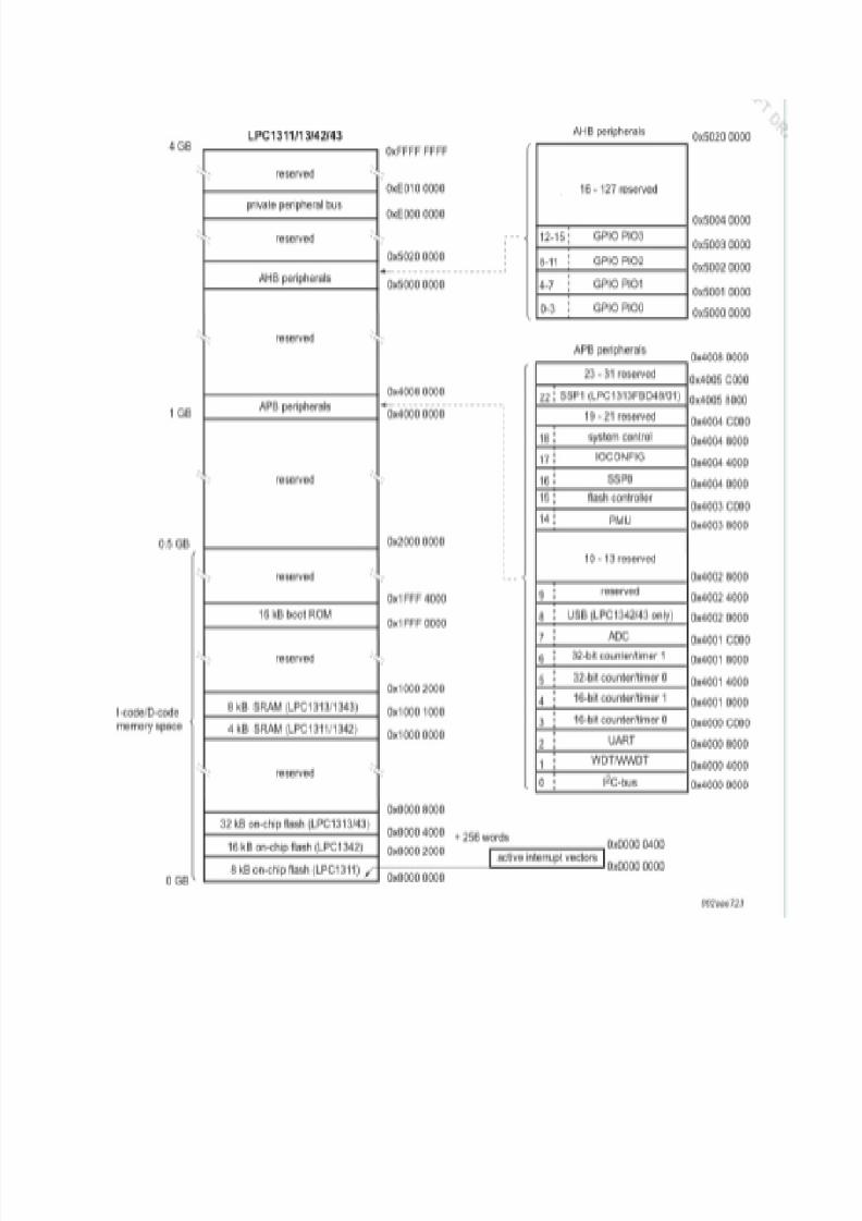
Memory:
Memory map:
The AHB peripheral area is 2 MB in size and is divided to allow for up to 128 peripherals. On
the LPC13xx, the GPIO ports are the only AHB peripherals. The APB peripheral area is 512 kb
in size and is divided to allow for up to 32 peripherals. Each peripheral of either type is allocated
16 kb of space. This allows simplifying the address decoding for each peripheral.All peripheral
register addresses are 32-bit word aligned regardless of their size. An implication of this is that
word and half-word registers must be accessed all at once. For example, it is not possible to read
or write the upper byte of a word register separately.
8/13/2019 Lpc1343 Introduction
http://slidepdf.com/reader/full/lpc1343-introduction 5/11

8/13/2019 Lpc1343 Introduction
http://slidepdf.com/reader/full/lpc1343-introduction 6/11
Pin diagram:

8/13/2019 Lpc1343 Introduction
http://slidepdf.com/reader/full/lpc1343-introduction 7/11
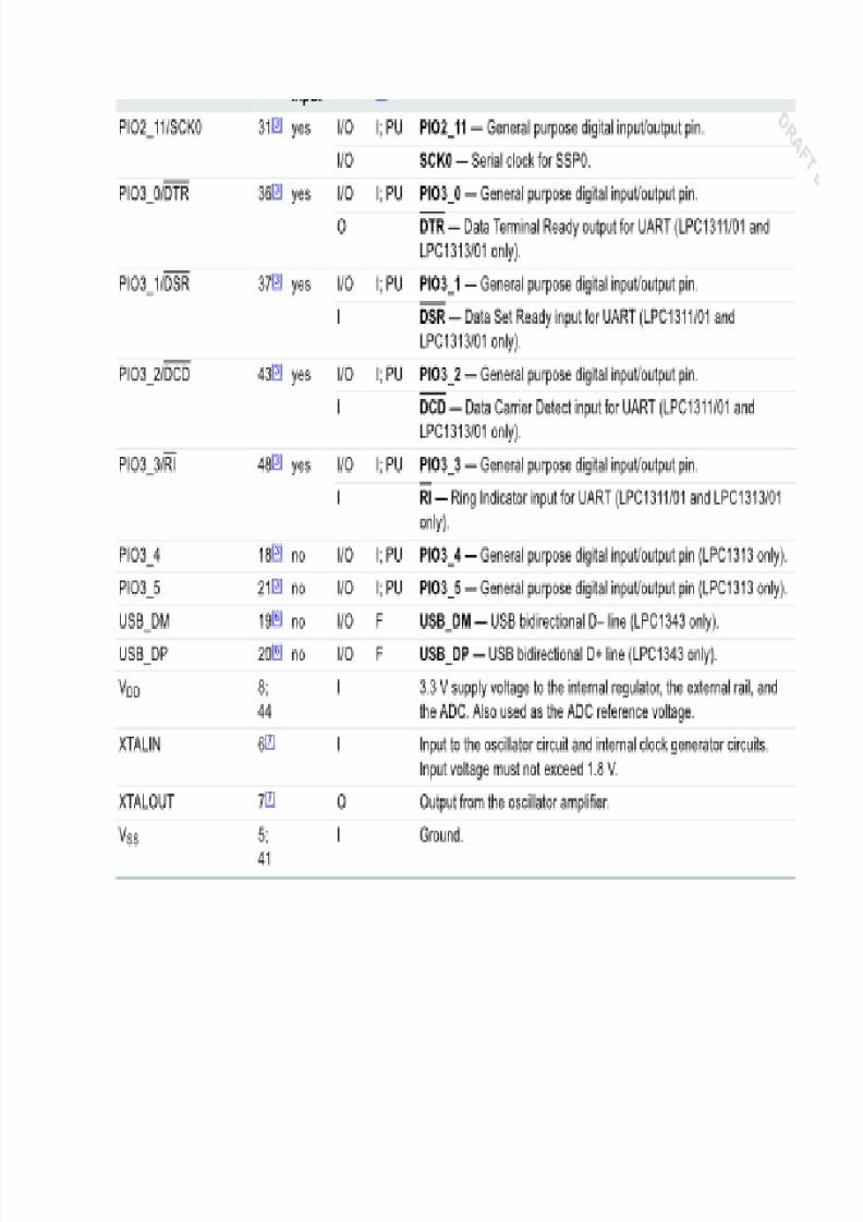
Pin description:

8/13/2019 Lpc1343 Introduction
http://slidepdf.com/reader/full/lpc1343-introduction 8/11

8/13/2019 Lpc1343 Introduction
http://slidepdf.com/reader/full/lpc1343-introduction 9/11
8/13/2019 Lpc1343 Introduction
http://slidepdf.com/reader/full/lpc1343-introduction 10/11
8/13/2019 Lpc1343 Introduction
http://slidepdf.com/reader/full/lpc1343-introduction 11/11
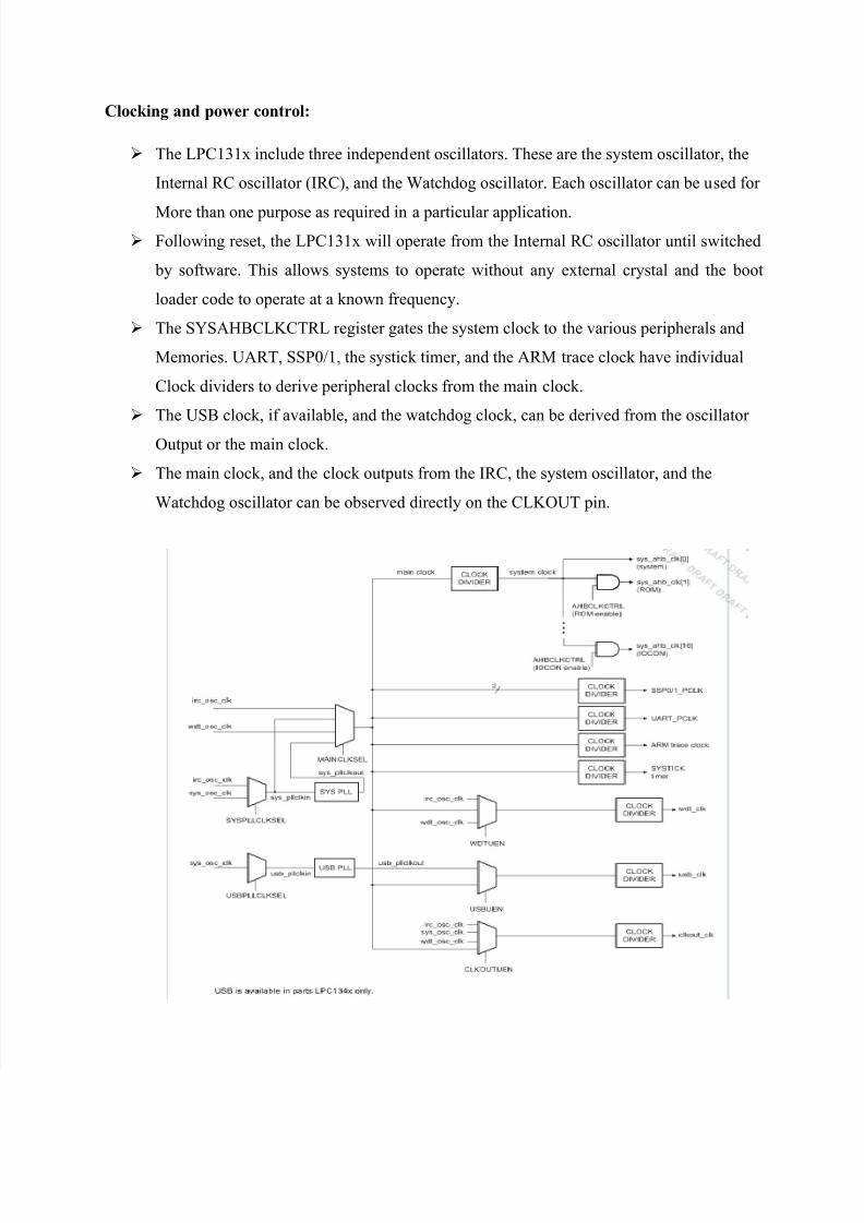
Clocking and power control:
The LPC131x include three independent oscillators. These are the system oscillator, the
Internal RC oscillator (IRC), and the Watchdog oscillator. Each oscillator can be used for
More than one purpose as required in a particular application.
Following reset, the LPC131x will operate from the Internal RC oscillator until switched
by software. This allows systems to operate without any external crystal and the boot
loader code to operate at a known frequency.
The SYSAHBCLKCTRL register gates the system clock to the various peripherals and
Memories. UART, SSP0/1, the systick timer, and the ARM trace clock have individual
Clock dividers to derive peripheral clocks from the main clock.
The USB clock, if available, and the watchdog clock, can be derived from the oscillator
Output or the main clock.
The main clock, and the clock outputs from the IRC, the system oscillator, and the
Watchdog oscillator can be observed directly on the CLKOUT pin.