ls1043a design checklist - nxp community
TRANSCRIPT

1 About this documentThis document provides recommendations for new designsbased on the LS1043A/LS1023A, which is a cost-effective,power-efficient, and highly integrated system-on-chip (SoC)design that extends the reach of the NXP Value Performanceline of QorIQ communications processors.
This document can also be used to debug newly-designedsystems by highlighting those aspects of a design that meritspecial attention during initial system start-up.
NOTEThis document applies to the LS1043A andLS1023A. For a list of functionalitydifferences, see the appendixes in LS1043A/LS1023A QorIQ Integrated MulticoreCommunications Processor ReferenceManual.
2 Before you beginEnsure you are familiar with the following NXP collateralbefore proceeding:
Freescale Semiconductor Document Number: AN5012
Application Note Rev. 0, 03/2016
LS1043A Design Checklist
© 2016 Freescale Semiconductor, Inc.
Contents
1 About this document........................... ...................... 1
2 Before you begin............................... ........................1
3 Simplifying the first phase of design.........................2
4 Power design recommendations.......... ..................... 5
5 Interface recommendations......................................14
6 Thermal................................ ................................... 63
7 Revision history.......................... ............................ 65
• LS1043A QorIQ Advanced Multicore Processor (LS1043A)• LS1023A QorIQ Advanced Multicore Processor (LS1023A)
3 Simplifying the first phase of designBefore designing a system with the chip, it is recommended that the designer be familiar with the available documentation,software, models, and tools.
This figure shows the major functional units within the LS1043A chip.
Watchpoint Cross Trigger
Trust Zone
Power Management
IFC, QuadSPI, SPI
2x DUART
32-bitDDR3L/4
Memory Controller
Real Time Debug
PerfMonitor
4x I2C, GPIO
Secure Boot
8x FlexTimer
QueueManager
BufferManager
Parse, classify,distribute
1/2.5/10G
PC
Ie 2
.0
SAT
A 3
.0Trace
4-Lane 10 GHz SerDes
ARM Cortex-A53 64b Cores
1G
SMMUs
3x USB3.0 w/PHY
CCI-400™ Coherency Fabric
32 KBD-Cache
32 KBI-Cache
ARM Cortex-A53 64b Cores
32 KBD-Cache
32 KBI-Cache
ARM Cortex-A53 64b Cores
32 KBD-Cache
32 KBI-Cache
ARM Cortex-A53 64b Cores
1G
1G
1G 1/2.5G1G
uQE
PC
Ie 2
.0
PC
Ie 2
.0
Frame ManagerSD/SDIO/eMMC
DMA
6x LPUART
Core ComplexAccelerators and Memory Control
Basic Peripherals, Interconnect and DebugNetworking Elements
SecurityEngine(SEC)
DPAA Hardware
ARM® Cortex®
A53 64b Core
32 KBD-Cache
32 KB I-Cache
1 MB L2 - Cache
Figure 1. LS1043A block diagram
This figure shows the major functional units within the LS1023A chip.
Simplifying the first phase of design
LS1043A Design Checklist , Rev. 0, 03/2016
2 Freescale Semiconductor, Inc.

Watchpoint Cross Trigger
Trust Zone
Power Management
IFC, QuadSPI, SPI
2x DUART
32-bitDDR3L/4
Memory Controller
Real Time Debug
PerfMonitor
4x I2C, GPIO
Secure Boot
8x FlexTimer
QueueManager
BufferManager
Parse, classify,distribute
1/2.5/10G
PC
Ie 2
.0
SAT
A 3
.0
Trace
4-Lane 10 GHz SerDes
ARM Cortex-A53 64b Cores
1G
SMMUs
3x USB3.0 w/PHY
CCI-400™ Coherency Fabric
32 KBD-Cache
32 KBI-Cache
ARM Cortex-A53 64b Cores
32 KBD-Cache
32 KBI-Cache
ARM Cortex-A53 64b Cores
32 KBD-Cache
32 KBI-Cache
ARM Cortex-A53 64b Cores
1G
1G
1G 1/2.5G1G
uQE
PC
Ie 2
.0
PC
Ie 2
.0
Frame ManagerSD/SDIO/eMMC
DMA
6x LPUART
Core ComplexAccelerators and Memory Control
Basic Peripherals, Interconnect and DebugNetworking Elements
SecurityEngine(SEC)
DPAA Hardware
ARM® Cortex®
A53 64b Core
32 KBD-Cache
32 KB I-Cache
1 MB L2 - Cache
Figure 2. LS1023A block diagram
3.1 Recommended resources
This table lists helpful tools, training resources, and documentation, some of which may be available only under a non-disclosure agreement (NDA). Contact your local field applications engineer or sales representative to obtain a copy.
Table 1. Helpful tools and references
ID Name Location
Related collateral
LS1043ACE LS1043AChip Errata
NOTE: This document describes the latest fixes and workarounds for thechip. It is strongly recommended that this document be thoroughlyresearched prior to starting a design with the chip.
Contact your NXPrepresentative
LS1043A LS1043A/LS1023A QorIQ Integrated Multicore Processor Data Sheet Contact your NXPrepresentative
QorIQLS1043A -Fact Sheet
LS1043A Fact Sheet Contact your NXPrepresentative
LS1043ARM LS1043A/LS1023A Integrated Multicore Processor Family Reference Manual Contact your NXPrepresentative
QorIQLS1043AProduct Brief
LS1043A/LS1023A Product Brief
Table continues on the next page...
Simplifying the first phase of design
LS1043A Design Checklist , Rev. 0, 03/2016
Freescale Semiconductor, Inc. 3

Table 1. Helpful tools and references (continued)
ID Name Location
AN5125 Introduction to Device Trees - Application note
Core Reference Manual Contact your NXPrepresentative
AN4871 Assembly Handling and Thermal Solutions for Lidless Flip Chip Ball GridArray Packages
www.nxp.com
QorIQ P1xxx series to LS1043A Migration Guide - Application Note www.nxp.com
Hardware and Layout Design Considerations for DDR4 SDRAM MemoryInterfaces - Application Note
www.nxp.com
Software tools
CodeWarrior Development Software for ARM® v8 64-bit based QorIQ LS-Series Processors
www.nxp.com
Software Development Kit for LS1043A www.nxp.com
Hardware tools
CodeWarrior TAP www.nxp.com
QorIQ LS Processor Probe Tips for CodeWarrior TAP www.nxp.com
QorIQ LS1043A reference design board www.nxp.com
Models
IBIS To ensure first path success, NXP strongly recommends using the IBISmodels for board-level simulations, especially for SerDes and DDRcharacteristics.
Contact your NXPrepresentative
BSDL Use the BSDL files in board verification. Contact your NXPrepresentative
Flotherm Use the Flotherm model for thermal simulation. Especially without forcedcooling or constant airflow, a thermal simulation should not be skipped.
Contact your NXPrepresentative
Available training
- Our third-party partners are part of an extensive alliance network. Moreinformation can be found at www.NXP.com/alliances.
www.nxp.com/alliances
- Training materials from past Smart Network Developer's Forums and NXPTechnology Forums (FTF) are also available at our website. These trainingmodules are a valuable resource for understanding the chip.
www.nxp.com/alliances
3.2 Product revisionsThis table lists the System Version Register (SVR) and ARM Core main ID register (TRCIDR1) values for the various chipsilicon derivatives.
Simplifying the first phase of design
LS1043A Design Checklist , Rev. 0, 03/2016
4 Freescale Semiconductor, Inc.

Table 2. Chip product revisions
Part DeviceRevision
ARM®Cortex®-A53
MPCoreProcessorRevision
ARM Core Main IDRegister
System VersionRegister Value
Note
LS1043A 1.0 r0p4 0x4100_0404h 0x8792_0110h Without Security
LS1043AE 1.0 r0p4 0x4100_0404h 0x8792_0010h With Security
LS1023AE 1.0 r0p4 0x4100_0404h 0x8792_0810h Without Security
LS1023A 1.0 r0p4 0x4100_0404h 0x8792_0910h With Security
4 Power design recommendations
4.1 Power pin recommendationsTable 3. Power and ground pin termination checklist
Signal name Signal type Used Not used Completed
AVDD_CGA1 I Power supply for cluster group A PLL 1 supply (1.8 Vthrough a filter)
Mustremainpowered
AVDD_CGA2 I Power supply for cluster group A PLL 2 supply (1.8 Vthrough a filter)
Mustremainpowered
AVDD_D1 I Power supply for DDR1 PLL (1.8 V through a filter) Mustremainpowered
AVDD_PLAT I Power supply for Platform PLL (1.8 V through a filter) Mustremainpowered
AVDD_SD1_PLL1 I Power supply for SerDes1 PLL 1 (SerDes, filtered fromX1VDD) (1.35 V)
Mustremainpowered(no need tofilter fromX1VDD)
AVDD_SD1_PLL2 I Power supply for SerDes1 PLL 2 (SerDes, filtered fromX1VDD) (1.35 V)
Mustremainpowered(no need tofilter fromX1VDD)
VDD I Core and platform supply voltage (1.0 V)
Table continues on the next page...
Power design recommendations
LS1043A Design Checklist , Rev. 0, 03/2016
Freescale Semiconductor, Inc. 5

Table 3. Power and ground pin termination checklist (continued)
Signal name Signal type Used Not used Completed
S1VDD I Core power supply for the SerDes logic transceiver Mustremainpowered
EVDD I eSDHC[0-3]/CLK/CMD,GPIO2,LPUART2_CTS_B,LPUART2_RTS_B,LPUART3,LPUART5, LPUART6,FTM4_CH6/7,FTM4_EXTCLK/FAULT/QD_PHA/QD_PHB (3.3 V / 1.8V)
Mustremainpowered
DVDD I DUART1/2, I2C, DMA, QE, LPUART1,LPUART2_SOUT/SIN, LPUART4, GPIO1, GPIO4,GIC (IRQ3/4/5/6/7/8/9/10), FTM 3/8, USB Control(DRVVBUS,PWRFAULT), FTM4_CH0/1/2/3/4/5 (3.3 V / 1.8 V)
Mustremainpowered
G1VDD I Power supply for the DDR3L/DDR4 (1.35 V / 1.2 V) Mustremainpowered
TVDD I Ethernet management interface 2 (EMI2) (1.2 V / 1.8 V /2.5 V)
Mustremainpowered
LVDD I Ethernet Interface 1/2, Ethernet management interface 1(EMI1), TSEC_1588, GPIO1, GPIO3,FTM1/2, GIC(IRQ11) (2.5 V/1.8 V)
Mustremainpowered
OVDD I IFC, SPI, GIC (IRQ 0/1/2), Temper_Detect, Systemcontrol and power management, SYSCLK,DDR_CLK,DIFF_SYSCLK, GPIO2, GPIO1,eSDHC[4-7]/VS/DAT123_DIR/DAT0_DIR/CMD_DIR/SYNC), Debug,SYSCLK, JTAG, RTC, FTM5/6/7,POR signals (1.8 V)
Mustremainpowered
X1VDD I Pad power supply for the SerDes transceiver (1.35 V) Mustremainpowered
TA_PROG_SFP I Should only be supplied 1.8V during secure boot programming. Fornormal operation, this pin needs to be tied to GND.
PROG_MTR I Should only be supplied 1.8V during secure boot programming. Fornormal operation, this pin needs to be tied to GND.
FA_VL - This pin must be pulled to GND -
TA_BB_VDD - Low power security monitor supply. This signal should beconnected to 1.0 V always on supply.
This signalshould beconnectedto 1.0 Vswitchablesupply.
TH_VDD I Reserved. Thermal monitor unit supply (1.8 V) Mustremainpowered
USB_HVDD I USB PHY Transceiver supply (3.3 V) Mustremainpowered(No
need to addfilter)
Table continues on the next page...
Power design recommendations
LS1043A Design Checklist , Rev. 0, 03/2016
6 Freescale Semiconductor, Inc.

Table 3. Power and ground pin termination checklist (continued)
Signal name Signal type Used Not used Completed
USB_SDVDD I Analog and Digital HS supply for USBPHY Mustremainpowered(No
need to addfilter)
USB_SVDD I Analog and Digital SS supply for USBPHY Mustremainpowered(No
need to addfilter)
SENSEVDD O VDD sense pin Do notconnect.This pinsshould beleft floating.
GND I Ground Tie to GND
SENSEGND O GND sense pin Do notconnect.This pinsshould beleft floating.
SD_GND I GND pin for SerDes and PLL supplies. Tie to GND
4.2 Power system-level recommendationsTable 4. Power design system-level checklist
Item Completed
General
Ensure that the ramp rate for all voltage supplies (including OVDD, DVDD, G1VDD, S1VDD, X1VDD, LVDD,EVDD, TVDD, OVDD all core and platform VDD supplies, D1_MVREF and all AVDD supplies.) follows therecommendations as mentined in "Power-on ramp rate" table in datasheet.
Ensure that VDD nominal voltage supply is set for 1.0 V with voltage tolerance of +/- 30 mV from thenominal VDD value.
Ensure that all other power supplies have a voltage tolerance as specified in "Recommended operatingconditions in datasheet., 1
Ensure that power supply is selected based on MAXIMUM power dissipation.1
Ensure the thermal design is based on THERMAL power dissipation.1
Ensure the power-up sequence is within 75 ms.1
Use large power planes to the extent possible.
Ensure the PLL filter circuit is applied to AVDD_PLAT, AVDD_CGA1, AVDD_CGA2, AVDD_D1.
Table continues on the next page...
Power design recommendations
LS1043A Design Checklist , Rev. 0, 03/2016
Freescale Semiconductor, Inc. 7

Table 4. Power design system-level checklist (continued)
Item Completed
If SerDes is enabled, ensure the PLL filter circuit is applied to the respective AVDD_SD1_PLL1,AVDD_SD1_PLL2. Otherwise, a filter is not required. Even if an entire SerDes module is not used, the poweris still needed to the AVDD pins. However, instead of using a filter, it needs to be connected to the XVDD railthrough a zero Ω resistor.
Ensure the PLL filter circuits are placed as close to the respective AVDD_SD1_PLL1, AVDD_SD1_PLL2 pinas possible.
Power supply decoupling
Provide sufficiently-sized power planes for the respective power rail. Use separate planes if possible; split(shared) planes if necessary. If split planes are used, ensure that signals on adjacent layers do not crosssplits. Avoid splitting ground planes at all costs.
Place at least one decoupling capacitor of 0.1μF (SMT ceremic chip) at each VDD, OVDD, DVDD, G1VDD,S1VDD, X1VDD, LVDD, EVDD, and TVDD pin of this chip
It is recommended that the decoupling capacitors receive their power from separate VDD, OVDD, DVDD,G1VDD, S1VDD, X1VDD, LVDD, EVDD, and TVDD and GND planes in the PCB, utilizing short traces tominimize inductance.
Capacitors may be placed directly under the chip using a standard escape pattern, and others may surroundthe part.
Ensure these capacitors have a value of at least 0.1μF. Recommended 0201.
Only use ceramic surface-mount technology (SMT) capacitors to minimize lead inductance, preferably 0402or 0603.
Distribute several bulk storage capacitors around the PCB, feeding the VDD and other planes (for example,DVDD, EVDD, LVDD, and G1VDD), to enable quick recharging of the smaller chip capacitors.
Ensure the bulk capacitors have a low equivalent series-resistance (ESR) rating to ensure the quickresponse time necessary.
Ensure the bulk capacitors are connected to the power and ground planes through two vias to minimizeinductance.
Ensure you work directly with your power regulator vendor for best values and types of bulk capacitors. Thecapacitors need to be selected to work well with the power supply to be able to handle the chip's powerrequirements. 2 Most regulators perform best with a mix of ceramic and very low ESR Tantalum typecapacitors.
As a guideline for customers and their power regulator vendors, Freescale recommends that these bulkcapacitors be chosen to maintain the positive transient power surges to less than +50 mV (negativetransient undershoot should comply with specification -30mV) for current steps of up to 2A with a slew rateof 1.5A/μs (10 A with a slew rate of 12A/μs).
Additional power supply decoupling
Use only SMT capacitors to minimize inductance.
Connections from all capacitors to power and ground must be done with multiple vias to further reduceinductance.
Ensure the board has at least one 0.1 μF SMT ceramic chip-capacitor as close as possible to each supplyball of the chip (S1VDD, X1VDD)
Where the board has blind vias, ensure these capacitors are placed directly below the chip supply andground connections.
Where the board does not have blind vias, ensure these capacitors are placed in a ring around the chip asclose to the supply and ground connections as possible.
For all SerDes supplies: Ensure there is a 1-µF ceramic chip capacitor on each side of the chip.
Table continues on the next page...
Power design recommendations
LS1043A Design Checklist , Rev. 0, 03/2016
8 Freescale Semiconductor, Inc.
Table 4. Power design system-level checklist (continued)
Item Completed
For all SerDes supplies: Ensure there is a 10-µF, low equivalent series resistance (ESR) SMT tantalumchip capacitor and a 100-µF, low ESR SMT tantalum chip capacitor between the device and any SerDesvoltage regulator.
PLL power supply filtering3
Provide independent filter circuits per PLL power supply, as illustrated in this figure.
1.8 V sourceR
C1 C2
GNDLow-ESL surface-mount capacitors
AVDD_PLAT, AVDD_D1AVDD_CGA1, AVDD_CGA2
• R = 5 Ω ± 5%• C1 = 10 μF ± 10%, 0603, X5R, with ESL ≤ 0.5 nH• C2 = 1.0 μF ± 10%, 0402, X5R, with ESL ≤ 0.5 nH• Low-ESL surface-mount capacitors
NOTE: A higher capacitance value for C2 may be used to improve the filter as long as the other C2parameters do not change (0402 body, X5R, ESL ≤ 0.5 nH).
NOTE: Voltage for AVDD is defined at the input of the PLL supply filter and not the pin of AVDD.
Ensure filter circuits use surface mount capacitors with minimum effective series inductance (ESL).
Place each circuit as close as possible to the specific AVDD pin being supplied to minimize noise coupledfrom nearby circuits.
NOTE: If done properly, it is possible to route directly from the capacitors to the AVDD pin, which is on theperiphery of the 621 (or 780) FC-PBGA footprint, without the added inductance of vias.
NOTE: It is recommended that an area fill or power plane split be provided to provide a low-impedanceprofile, which helps keep nearby crosstalk noise from inducing unwanted noise.
Ensure each of the PLLs is provided with power through independent power supply pins (AVDD_CGA1,AVDD_CGA2, AVDD_PLAT, AVDD_D1, AVDD_SD1_PLL1, and AVDD_SD1_PLL2, respectively).
For maximum effectiveness, ensure the filter circuit is placed as close as possible to the AVDD_SD1_PLLnball to ensure it filters out as much noise as possible.
Ensure the ground connection is near the AVDD_SD1_PLLn ball. The 0.003-μF capacitor is closest to theball, followed by a 4.7-μF capacitor and 47-μF capacitor, and finally the 0.33-Ω resistor to the boardsupplyplane.
To ensure stability of the internal clock, ensure the power supplied to the PLL is filtered using a circuit similarto the one shown in this figure.
• AVDD_SD1_PLLn should be a filtered version of X1VDD.• Signals on the SerDes interface are fed from the X1VDD power plane.• It is recommended that an area fill or power plane split be provided for both AVDD and AGND to
provide a low-impedance profile, which helps keep nearby crosstalk noise from inducing unwantednoise.
• Voltage for AVDD_SD1_PLLn is defined at the PLL supply filter and not the pin of AVDD_SD1_PLLn.• A 47 μF 0805 XR5 or XR7, 4.7 μF 0603, and 0.003 μF 0402 capacitor are recommended. The size
and material type are important. A 0.33 Ω ± 1% resistor is recommended.• Caution: These filters are a necessary extension of the PLL circuitry and are compliant with the
device specifications. Any deviation from the recommended filters is done at the user's risk.
Table continues on the next page...
Power design recommendations
LS1043A Design Checklist , Rev. 0, 03/2016
Freescale Semiconductor, Inc. 9

Table 4. Power design system-level checklist (continued)
Item Completed
X1VDD0.33 Ω
AVDD_SD1_PLLn
47 µF 4.7 µF 0.003 µF
SD_GND
Caution: These filters are a necessary extension of the PLL circuitry and are compliant with the devicespecifications. Any deviation from the recommended filters is done at the user's risk.
Ensure the capacitors are connected from AVDD_SD1_PLLn to the ground plane.
Use ceramic chip capacitors with the highest possible self-resonant frequency. All traces should be keptshort, wide, and direct.
Ensure AVDD_SD1_PLLn is a filtered version of X1VDD
Ensure that signals on the SerDes interface are fed from the X1VDD power plane.
S1VDD should be supplied by a linear regulator and needs a nominal voltage of 1.0V. An example solutionfor S1VDD filtering, where S1VDD is sourced from a linear regulator, is shown in the following figure. Thecomponent values in this example filter are system-dependent and are still under characterization, socomponent values may need adjustment based on the system or environment noise.
Where:
• C1 = 0.003 μF ± 10%, X5R, with ESL ≤ 0.5 nH• C2 and C3 = 2.2 μF ± 10%, X5R, with ESL ≤ 0.5 nH• F1 and F2 = 120 Ω at 100 MHz 2A 25% 0603 Ferrite (for example, Murata BLM18KG121TN1)• Bulk and decoupling capacitors are added, as needed, per power supply design.
S1VDDLinear regulator output
C1C2C3
GND
Bulk and decoupling capacitors
F1
F2
NOTE: See section "Power-on ramp rate" in the applicable chip data sheet for maximum SnVDD power-upramp rate.
NOTE: There must be enough output capacitance or a soft-start feature to assure the ramp-raterequirement is met.
NOTE: The ferrite beads should be placed in parallel to reduce voltage droop.NOTE: Besides a linear regulator, a low-noise-dedicated switching regulator can be used. 10 mVp-p, 50
kHz-500 MHz is the noise goal.
X1VDD may be supplied by a linear regulator or sourced by a filtered G1VDD. Systems may design-in bothoptions to allow flexibility to address system noise dependencies. However, for initial system bring-up, thelinear regulator option is highly recommended. An example solution for XnVDD filtering, where XnVDD issourced from a linear regulator, is shown in the following figure. The component values in this example filterare system-dependent and are still under characterization, so component values may need adjustmentbased on the system or environment noise.
Where:
• C1 = 0.003 μF ± 10%, X5R, with ESL ≤ 0.5 nH• C2 and C3 = 2.2 μF ± 10%, X5R, with ESL ≤ 0.5 nH• F1 and F2 = 120 Ω at 100 MHz 2A 25% 0603 Ferrite (for example, Murata BLM18KG121TN1)• Bulk and decoupling capacitors are added, as needed, per power supply design.
Table continues on the next page...
Power design recommendations
LS1043A Design Checklist , Rev. 0, 03/2016
10 Freescale Semiconductor, Inc.
Table 4. Power design system-level checklist (continued)
Item Completed
X1VDDLinear regulator output
C1C2C3
GND
Bulk and decoupling capacitors
F1
F2
NOTE: See section "Power-on ramp rate" in the applicable chip data sheet for maximum XnVDD power-upramp rate.
NOTE: There must be enough output capacitance or a soft-start feature to assure the ramp-raterequirement is met.
NOTE: The ferrite beads should be placed in parallel to reduce voltage droop.NOTE: Besides a linear regulator, a low-noise-dedicated switching regulator can be used. 10 mVp-p, 50
kHz-500 MHz is the noise goal.
USB_HVDD must be sourced by a filtered 3.3V voltage source using a star connection. An example solutionfor USB_HVDD filtering, where USB_HVDD is sourced from a 3.3V voltage source, is illustrated in thefollowing figure. The component values in this example filter are system-dependent and are still undercharacterization, so component values may need adjustment based on the system or environment noise.
Where:
• C1 = 0.003 μF ± 10%, X5R, with ESL ≤ 0.5 nH• C2 and C3 = 2.2 μF ± 10%, X5R, with ESL ≤ 0.5 nH• F1 = 120 Ω at 100 MHz 2A 25% 0603 Ferrite (for example, Murata BLM18KG121TN1)• Bulk and decoupling capacitors are added, as needed, per power supply design.
USB_HVDD3.3-V source
C1C2C3
GND
Bulk and decoupling capacitors
F1
USB_SDVDD must be sourced by a filtered VDD using a star connection. An example solution forUSB_SDVDD filtering, where USB_SDVDD is sourced from VDD, is illustrated in the following figure. Thecomponent values in this example filter are system-dependent and are still under characterization, socomponent values may need adjustment based on the system or environment noise.
Where:
• C1 = 2.2 μF ± 20%, X5R, with low ESL (for example, Panasonic ECJ0EB0J225M)• F1 = 120 Ω at 100-MHz 2A 25% Ferrite (for example, Murata BLM18KG121TN1)• Bulk and decoupling capacitors are added, as needed, per power supply design
USB_SnVDDVDD
C1
GND
Bulk and decoupling capacitors
F1
C1
Use ceramic chip capacitors with the highest possible self-resonant frequency. All traces should be keptshort, wide, and direct.
Power design recommendations
LS1043A Design Checklist , Rev. 0, 03/2016
Freescale Semiconductor, Inc. 11

1. See the applicable chip data sheet for more details.2. Suggested bulk capacitors are 100-330 μF (AVX TPS tantalum or Sanyo OSCON).3. The PLL power supply filter circuit filters noise in the PLLs' resonant frequency range from 500 kHz-10 MHz.
4.3 Power-on reset recommendations
Various chip functions are initialized by sampling certain signals during the assertion of PORESET_B. These power-on reset(POR) inputs are pulled either high or low during this period. While these pins are generally output pins during normaloperation, they are treated as inputs while PORESET_B is asserted. When PORESET_B de-asserts, the configuration pinsare sampled and latched into registers, and the pins then take on their normal output circuit characteristics.
Table 5. Power-on reset system-level checklist
Item Completed
Ensure PORESET_B is asserted for a minimum of 1 ms.
Ensure HRESET_B is asserted for a minimum of 32 SYSCLK cycles.
In cases where a configuration pin has no default, use a 4.7 kΩ pull-up or pull-down resistor for appropriateconfiguration of the pin.
Optional: An alternative to using pull-up and pull-down resistors to configure the POR pins is to use a PLD orsimilar device that drives the configuration signals to the chip when HRESET_B is asserted. The PLD mustbegin to drive these signals at least four SYSCLK cycles prior to the de-assertion of PORESET_B (PLLconfiguration inputs must meet a 100 µs set-up time to HRESET_B), hold their values for at least twoSYSCLK cycles after the de-assertion of PORESET_B, and then release the pins to high impedanceafterward for normal device operation
NOTE: See the applicable chip data sheet for details about reset initialization timing specifications.
Configuration settings
Ensure the settings in Configuration signals sampled at reset are selected properly.
NOTE: See the applicable chip reference manual for a more detailed description of each configurationoption.
Power sequencing
The chip requires that its power rails be applied in a specific sequence in order to ensure proper deviceoperation. Please refer to "QorIQ LS1043A, LS1023A Data Sheet" for details.
4.3.1 Configuration signals sampled at resetThe signals that serve alternate functions as configuration input signals during system reset are summarized in this table.
Reset configuration signals are sampled at the negation of PORESET_B. However, there is a setup and hold time for thesesignals relative to the rising edge of PORESET_B, as described in the chip's data sheet document.
The reset configuration signals are multiplexed with other functional signals. The values on these signals during reset areinterpreted to be logic one or zero, regardless of whether the functional signal name is defined as active-low. The resetconfiguration signals have internal pull-up resistors so that if the signals are not driven, the default value is high (a one), asshown in the table. Some signals must be driven high or low during the reset period. For details about all the signals thatrequire external pull-up resistors, see the applicable device data sheet.
Power design recommendations
LS1043A Design Checklist , Rev. 0, 03/2016
12 Freescale Semiconductor, Inc.
Table 6. LS1043A reset configuration signals
Configuration Type Functional Pins Comments
Reset configuration word (RCW) sourceinputs cfg_rcw_src[0:8]
IFC_AD[8:15]
IFC_CLE
They must be set to one of the validoptions. The 512 bit RCW word has all thenecessary configuration information for thechip. If there is no valid RCW in theexternal memory, it can be programmedusing the Code Warrior or otherprogrammer. The JTAG configuration filescan be used in the following situations:
• target boards that do not have RCWalready programmed
• new board bring up• recovering boards with blank or
damaged flash
IFC external transceiver enable polarityselect (cfg_ifc_te)
IFC_TE Default is "1"
DRAM type select (cfg_dram_type) IFC_A[21] Default is DDR3L. This reset configutationpin selects the porper I/O voltage:DDR3L=1.35V or DDR4=1.2V. Ensure theselection value that matches the DDR typeused on board.
General-purpose input (cfg_gpinput[0:7]) IFC_AD[0:7] Default "1111 1111", values can beapplication defined
"Single Oscillator Source" clock select.
This field selects between SYSCLK(Single ended) and DIFF_SYSCLK/DIFF_SYSCLK_B (differential) inputs.
(cfg_eng_use0)
IFC_WE0_B 0=DIFF_SYSCLK/DIFF_SYSCLK_B(differential)
1=SYSCLK (single ended)
Default selection is single ended SYSCLK;"1"
"Single Oscillator Source" clock.
This field indicates whether on-chipLVDS termination for differential clock isenabled or disabled.
configuration (cfg_eng_use1)
IFC_OE_B 0 = Disabled (MUST make sure thatExternal termination pads ofDIFF_SYSCLK/DIFF_SYSCLK_B haveproper termination)
1 = Enabled (default)
Default is "1".
It is recommened to keep provision foroptional pull-down resistor on board.
"Single Oscillator Source" clockconfiguration (cfg_eng_use2)
IFC_WP0_B Default is "1". Reserved.
It is recommened to keep provision foroptional pull-down resistor on board.
NOTE1. The hardcoded RCW can be used as an alternative method for initial board bring up
when there is no valid RCW in the external memory. For more information, see thehardcoded RCW table below.
Power design recommendations
LS1043A Design Checklist , Rev. 0, 03/2016
Freescale Semiconductor, Inc. 13

This table shows the some basic hardcoded RCW values. For details please refer to LS1043A Reference Manual.
Table 7. Hardcoded RCW values
Harcoded RCW
cfg_rcw_src[0:8] 9'b0_1001_1010 (0x9A) 9'b0_1001_1110 (0x9E)
SYSCLK (MHz) 66 100
DDRCLK (MHz) 100 100
PLL configuration
SYS_PLL_RAT 4:1 3:1
RCW[2:6] 5'd4 5'd3
MEM_PLL_RAT 13:1 13:1
RCW[10:15] 6'd13 6'd13
CGA_PLL1_RAT 18:1 12:1
RCW[26:31] 6'd18 6'd12
CGA_PLL2_RAT 15:1 10:1
RCW[34:39] 6'd15 6'd10
C1_PLL_SEL CGA_PLL1 / 1 CGA_PLL1 / 1
If a new board is using a blank flash and flash is the source of RCW, then the all 0xff value from flash for RCW will put thedevice in an unknown state.
There are two methods to work around this problem:
1. Put switches on cfg_rcw_src signals to choose hardcoded RCW(0x9A, 0x9E).
2. Use CodeWarrior tool from Freescale to override RCW.”
5 Interface recommendations
5.1 DDR controller recommendationsLS1043A/LS1023A supports DDR3L(1.35V) and DDR4(1.2V) SDRAM
The memory interface controls main memory accesses. The interface supports 32 bit data access.
5.1.1 DDR controller pin termination recommendationsTable 8. DDR controller pin termination checklist
Signal Name1 I/Otype
Used Not used Completed
DDR3L Signal DDR4 Signal
D1_MA[13:00]
D1_MA[14]
D1_MA[15]
D1_MA[13:00]
D1_MBG1
D1_MACT_B
O Must be properly terminated toVTT
These pins can be leftunconnected.
Table continues on the next page...
Interface recommendations
LS1043A Design Checklist , Rev. 0, 03/2016
14 Freescale Semiconductor, Inc.

Table 8. DDR controller pin termination checklist (continued)
Signal Name1 I/Otype
Used Not used Completed
DDR3L Signal DDR4 Signal
D1_MBA[0:1]
D1_MBA[2]
D1_MBA[0:1]
D1_MBG0
O Must be properly terminated toVTT
These pins can be leftunconnected.
D1_MCK[0:1]/D1_MCK[0:1]_B O These pins must be properlyterminated.
These pins may be leftunconnected.
D1_MCKE[0:1] O Must be properly terminated toVTT
These pins are actively drivenduring reset instead of beingreleased to high impedance.
These pins can be leftunconnected.
D1_MCS[0:3]_B O Must be properly terminated toVTT
These pins can be leftunconnected.
D1_MDIC[0:1] I/O • These pins are used forautomatic calibration ofthe DDR3L/DDR4 IOs.The MDIC[0:1] pins mustbe connected to 162Ωprecision 1% resistors.
• MDIC[0] is groundedthrough a 162Ω precision1% resistor and MDIC[1]is connected to GVDDthrough a 162Ω precision1% resistor.
• For either full- or half-driver strength calibrationof DDR IOs, use thesame MDIC resistorvalue of 162 Ω.
• The memory controllerregister setting can beused to determine ifautomatic calibration isdone to full- or half-drivestrength.
These pins can be leftunconnected.
D1_MDM[0:3],
D1_MDM[8]
O - These pins can be leftunconnected.
D1_MDQ[0:32] I/O - These pins can be leftunconnected.
D1_MDQS[0:3]/D1_MDQS[0:3]_B,D1_MDQS[8]/D1_MDQS[8]_B
I/O - These pins can be leftunconnected.
D1_MECC[0:3] I/O - These pins can be leftunconnected.
D1_MAPAR_ERR_B
D1_MALERT_B O This pin is an open drain outputfrom registered DIMMs. Ensurethat a 2-10 kΩ pull-up to G1VDDis present on this pin.
This pin should be pulled up.
Table continues on the next page...
Interface recommendations
LS1043A Design Checklist , Rev. 0, 03/2016
Freescale Semiconductor, Inc. 15

Table 8. DDR controller pin termination checklist (continued)
Signal Name1 I/Otype
Used Not used Completed
DDR3L Signal DDR4 Signal
D1_MAPAR O If the controller supports theoptional MAPAR andMAPAR_ERR signals, ensurethat they are hooked up asfollows:
• MAPAR_OUT (from thecontroller) => PAR_IN (atthe RDIMM)
• ERR_OUT (from theRDIMM) =>MAPAR_ERR (at thecontroller)
This pin can be leftunconnected.
D1_MODT[0:1] O Ensure the MODT signals areconnected correctly. Two dualranked DIMMs topology is notsupported on LS1043A.
For a single, dual-rankedDIMM, consider the followingconnections
• MODT(0), MCS(0),MCKE(0)
• MODT(1), MCS(1),MCKE(1)
For quad-ranked DIMMS, it isrecommended to obtain a datasheet from the memory supplierto confirm required signals. Butin general, each controllerneeds MCS(0:3), MODT(0:1),and MCKE(0:1) connected tothe one quad-ranked DIMM.
These pins are actively drivenduring reset instead of beingreleased to high impedance.
These pins can be leftunconnected.
D1_MRAS_B O Must be properly terminated toVTT
This pin can be leftunconnected.
D1_MCAS_B O Must be properly terminated toVTT
This pin can be leftunconnected.
D1_MWE_B O Must be properly terminated toVTT
This pin can be leftunconnected.
D1_MVREF DDR4 Vref isprovided
internally, theexternal vref
signal needs to begrounded when
using DDR4SDRAM
I DDR reference voltage: 0.49 xGVDD to 0.51 x G1VDD.D1_MVREF can be generatedusing a divider from G1VDD asMVREF. Another option is touse supplies that generateG1VDD, VTT, and D1_MVREFvoltage. These methods helpreduce differences between
This pin must be connected toGND.
Interface recommendations
LS1043A Design Checklist , Rev. 0, 03/2016
16 Freescale Semiconductor, Inc.

Table 8. DDR controller pin termination checklist
Signal Name1 I/Otype
Used Not used Completed
DDR3L Signal DDR4 Signal
G1VDD and MVREF.D1_MVREF generated from aseparate regulator is notrecommended, becauseD1_MVREF does not trackG1VDD as closely.
1. DDR3L signals are muxed with DDR4 signals and shown in this table
5.1.2 DDR system-level recommendationsTable 9. DDR system-level checklist
Item Completed
General
DDR3L /DDR4 mode selection is through por-config signal cfg_dram_type. Ensure that the pin is configuredcorrectly as per the DDR mode. Setting DDR4 mode while applying GVdd=1.35V can lead to damage ofIO's.
Data Bus inversion (DBI) signals are muxed on Data Mask (D1_MDM) signals and are optional function forDDR4. Only one function can be used at a time.
PORESET_B assertion should also reset SDRAM Memory.
NOTE1. Stacked memory for DDR4 are not supported2. DDR4 RDIMM are not supported.3. For devices with 4 ECC pins, ensure to connect one of the ECC pins to the Prime
DQ of ECC DRAM.
5.2 IFC pin termination recommendationsTable 10. IFC pin termination checklist
Signal name I/O type Used Not used Completed
IFC_A[16:20] O These pins must not be pulled down during power-on reset. It may be pulledup, driven high, or if there are no externally connected devices, left in tristate.If these pins are connected to a device that pulls down during reset, anexternal pull-up is required to drive these pins to a safe state during reset.
IFC_A[21] O This pin is a reset configuration pin. It has a weak (~20 kΩ ) internal pull-up P-FET that is enabled only when the processor is in its reset state. The pull-upis designed such that it can be overpowered by an external 4.7 kΩ resistor.However, if the signal is intended to be high after reset, and if there is anydevice on the net that might pull down the value of the net at reset, a pull-upor active driver is needed.
Table continues on the next page...
Interface recommendations
LS1043A Design Checklist , Rev. 0, 03/2016
Freescale Semiconductor, Inc. 17
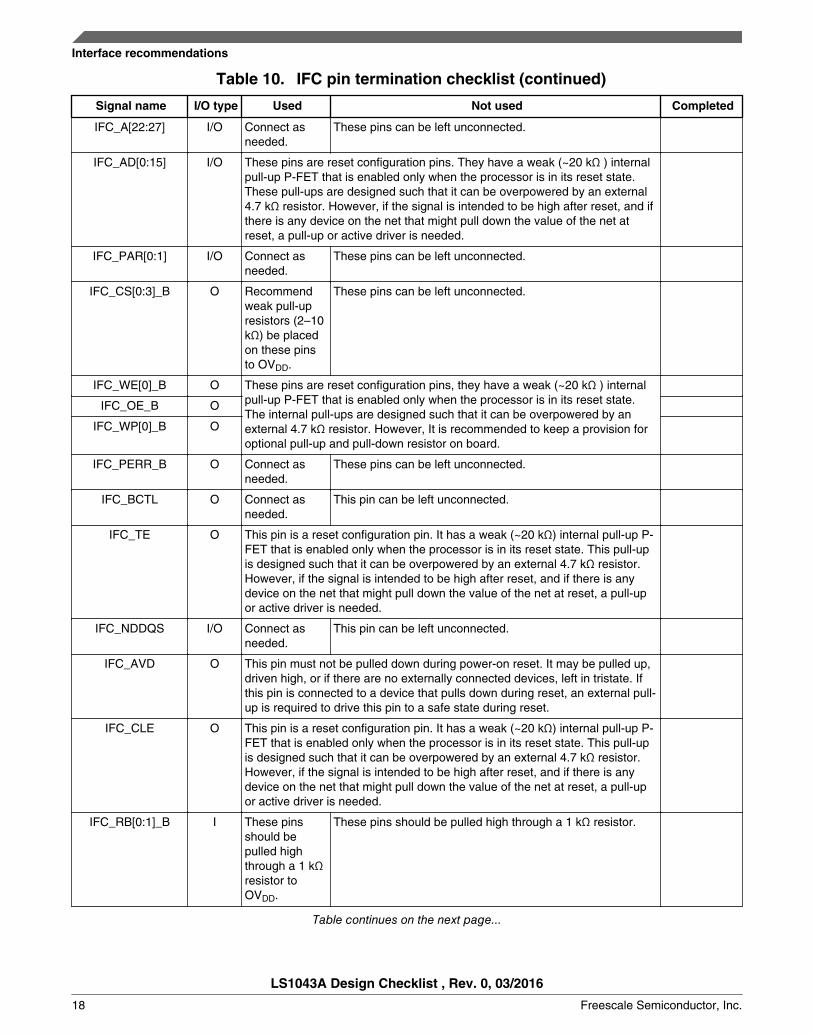
Table 10. IFC pin termination checklist (continued)
Signal name I/O type Used Not used Completed
IFC_A[22:27] I/O Connect asneeded.
These pins can be left unconnected.
IFC_AD[0:15] I/O These pins are reset configuration pins. They have a weak (~20 kΩ ) internalpull-up P-FET that is enabled only when the processor is in its reset state.These pull-ups are designed such that it can be overpowered by an external4.7 kΩ resistor. However, if the signal is intended to be high after reset, and ifthere is any device on the net that might pull down the value of the net atreset, a pull-up or active driver is needed.
IFC_PAR[0:1] I/O Connect asneeded.
These pins can be left unconnected.
IFC_CS[0:3]_B O Recommendweak pull-upresistors (2–10kΩ) be placedon these pinsto OVDD.
These pins can be left unconnected.
IFC_WE[0]_B O These pins are reset configuration pins, they have a weak (~20 kΩ ) internalpull-up P-FET that is enabled only when the processor is in its reset state.The internal pull-ups are designed such that it can be overpowered by anexternal 4.7 kΩ resistor. However, It is recommended to keep a provision foroptional pull-up and pull-down resistor on board.
IFC_OE_B O
IFC_WP[0]_B O
IFC_PERR_B O Connect asneeded.
These pins can be left unconnected.
IFC_BCTL O Connect asneeded.
This pin can be left unconnected.
IFC_TE O This pin is a reset configuration pin. It has a weak (~20 kΩ) internal pull-up P-FET that is enabled only when the processor is in its reset state. This pull-upis designed such that it can be overpowered by an external 4.7 kΩ resistor.However, if the signal is intended to be high after reset, and if there is anydevice on the net that might pull down the value of the net at reset, a pull-upor active driver is needed.
IFC_NDDQS I/O Connect asneeded.
This pin can be left unconnected.
IFC_AVD O This pin must not be pulled down during power-on reset. It may be pulled up,driven high, or if there are no externally connected devices, left in tristate. Ifthis pin is connected to a device that pulls down during reset, an external pull-up is required to drive this pin to a safe state during reset.
IFC_CLE O This pin is a reset configuration pin. It has a weak (~20 kΩ) internal pull-up P-FET that is enabled only when the processor is in its reset state. This pull-upis designed such that it can be overpowered by an external 4.7 kΩ resistor.However, if the signal is intended to be high after reset, and if there is anydevice on the net that might pull down the value of the net at reset, a pull-upor active driver is needed.
IFC_RB[0:1]_B I These pinsshould bepulled highthrough a 1 kΩresistor toOVDD.
These pins should be pulled high through a 1 kΩ resistor.
Table continues on the next page...
Interface recommendations
LS1043A Design Checklist , Rev. 0, 03/2016
18 Freescale Semiconductor, Inc.

Table 10. IFC pin termination checklist (continued)
Signal name I/O type Used Not used Completed
IFC_CLK[0:1] O Connect asneeded.
This pin can be left unconnected.
IFC_NDDDR_CLK O Connect asneeded
This pin can be left unconnected.
NOTE
IFC interface is on OVDD power domain which is 1.8V only
For functional connection diagram, refer chip reference manual.
5.3 DUART pin termination recommendationsTable 11. DUART pin termination checklist
Signal name I/O type Used Not used Completed
UART1_SOUT O The functionality of these pinsisdetermined by the UART_BASEandUART_EXT fields in theresetconfigurationword(RCW[UART_BASE],RCW[UART_EXT]).
These pins can be left unconnected.
UART1_RTS_B O
UART1_SIN I Program as GPIO and output.
UART1_CTS_B I This pin should be pulled high through a2-10 kΩ resistor to DVDD or elseprogrammed as GPIO and output
UART2_SOUT O This pin can be left unconnected.
UART2_RTS_B O
UART2_SIN I Program as GPIO and output.
UART2_CTS_B I This pin should be pulled high through a2-10 kΩ resistor to DVDD or elseprogrammed as GPIO and output
UART3_SOUT O This pin can be left unconnected.
UART3_SIN I Program as GPIO and output.
UART4_SOUT O This pin can be left unconnected.
UART4_SIN I Programas GPIO and output.
5.4 LPUART pin termination recommendations
Table 12. LPUART pin termination checklist
Signal Name IO type Used Not Used Completed
LPUART[1:3]_CTS_B I The functionality ofLPUART1_CTS_B is determinedby the UART_BASE and
Program as GPIOs and outputs.
Table continues on the next page...
Interface recommendations
LS1043A Design Checklist , Rev. 0, 03/2016
Freescale Semiconductor, Inc. 19

Table 12. LPUART pin termination checklist (continued)
Signal Name IO type Used Not Used Completed
UART_EXT fields in the resetconfiguration word(RCW[UART_BASE],RCW[UART_EXT]).
The functionality ofLPUART[2:3]_CTS_B isdetermined by the SDHC_BASEand SDHC_EXT fields in the resetconfiguration word(RCW[SDHC_BASE],RCW[SDHC_EXT]).
LPUART[1:3]_RTS_B O The functionality ofLPUART1_RTS_B is determinedby the UART_BASE andUART_EXT fields in the resetconfiguration word(RCW[UART_BASE],RCW[UART_EXT]).
The functionality ofLPUART[2:3]_RTS_B isdetermined by the SDHC_BASEand SDHC_EXT fields in the resetconfiguration word(RCW[SDHC_BASE],RCW[SDHC_EXT]).
Program as GPIOs and outputs.
LPUART[1:6]_SIN I The functionality ofLPUART[1:2]_SIN andLPUART[4]_SIN is determined bythe UART_BASE and UART_EXTfields in the reset configurationword (RCW[UART_BASE],RCW[UART_EXT]).
The functionality ofLPUART[5:6]_SIN andLPUART[3]_SIN is determined bythe SDHC_BASE and SDHC_EXTfields in the reset configurationword (RCW[SDHC_BASE],RCW[SDHC_EXT]).
Program as GPIOs and outputs.
LPUART[1:6]_SOUT O The functionality ofLPUART[1:2]_SOUT andLPUART[4]_SOUT is determinedby the UART_BASE andUART_EXT fields in the resetconfiguration word(RCW[UART_BASE],RCW[UART_EXT]).
The functionality ofLPUART[5:6]_SOUT andLPUART[3]_SOUT is determinedby the SDHC_BASE andSDHC_EXT fields in the reset
Program as GPIOs and outputs.
Interface recommendations
LS1043A Design Checklist , Rev. 0, 03/2016
20 Freescale Semiconductor, Inc.

Table 12. LPUART pin termination checklist
Signal Name IO type Used Not Used Completed
configuration word(RCW[SDHC_BASE],RCW[SDHC_EXT]).
5.5 I2C pin termination recommendationsTable 13. I2C pin termination checklist
Signal Name I/O type Used Not used Completed
IIC1_SDA I/O Tie these open-drain signals high througha nominal 1 kΩ resistor to DVDD. Optimumpull-up value depends on the capacitiveloading of external devices and requiredoperating speed.
These pins should be pulled high througha 2-10 kΩ resistor to DVDD.IIC1_SCL I/O
IIC2_SDA I/O The functionality of this signal isdetermined by the IIC2_EXT andIIC2_BASE field in the reset configurationword (RCW[IIC2_EXT]) and(RCW[IIC2_BASE]). Recommendthat aweak pull-up resistor (1 kΩ)be placed onthis pin to theres pective powersupply.This pin is an open-drain signal.
If I2C2 is not used, all pins can beprogrammed as GPIO's and output.IIC2_SCL I/O
IIC3_SDA I/O The functionality of this signal isdetermined by theSCFG_RCWPMUXCR0 register.Recommend that a weak pull-up resistor(1 kΩ)be placed on this pin to therespective power supply.This pin is an open-drain signal.
If I2C3 is not used, all pins can beprogrammed as GPIO's and output.IIC3_SCL I/O
IIC4_SDA I/O The functionality of this signal isdetermined by theSCFG_RCWPMUXCR0 register.Recommend that a weak pull-up resistor(1 kΩ) be placed on this pin to therespective power supply.This pin is an open-drain signal.
If I2C4 is not used, all pins can beprogrammed as GPIO's and output.IIC4_SCL I/O
5.6 eSDHC recommendationsThe LS1043A/LS1023A eSDHC interface supports a large variety of devices
• SDXC cards Upto 2TB space, with UHS-I speed grade• UHS-I (Ultra high speed grade) SDR12, SDR25, SDR50, SDR104, DDR50 are supported• UHS-I cards work on 1.8V signaling
Interface recommendations
LS1043A Design Checklist , Rev. 0, 03/2016
Freescale Semiconductor, Inc. 21
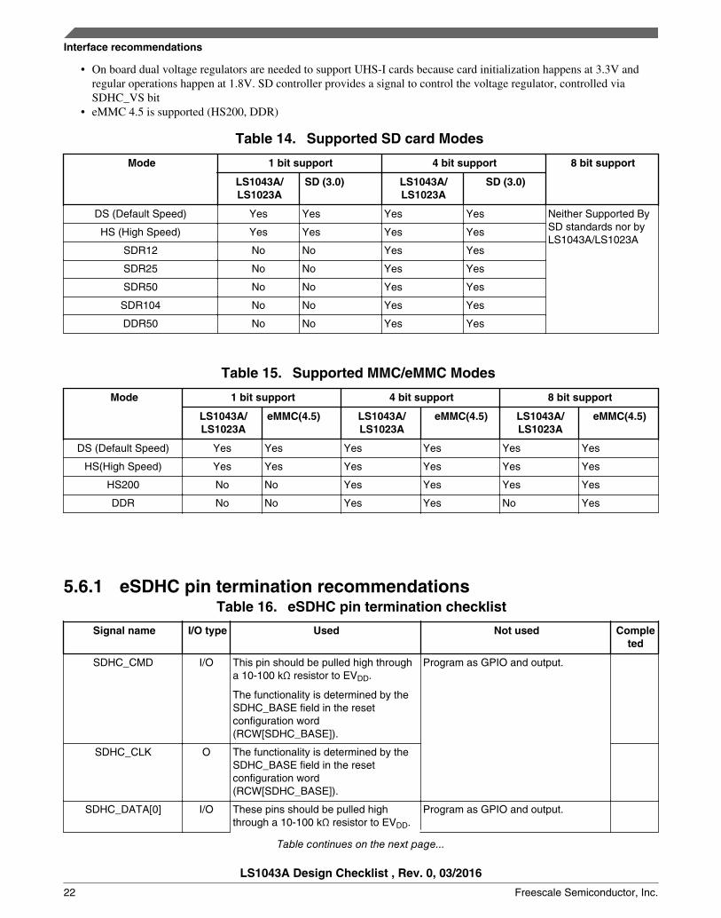
• On board dual voltage regulators are needed to support UHS-I cards because card initialization happens at 3.3V andregular operations happen at 1.8V. SD controller provides a signal to control the voltage regulator, controlled viaSDHC_VS bit
• eMMC 4.5 is supported (HS200, DDR)
Table 14. Supported SD card Modes
Mode 1 bit support 4 bit support 8 bit support
LS1043A/LS1023A
SD (3.0) LS1043A/LS1023A
SD (3.0)
DS (Default Speed) Yes Yes Yes Yes Neither Supported BySD standards nor byLS1043A/LS1023A
HS (High Speed) Yes Yes Yes Yes
SDR12 No No Yes Yes
SDR25 No No Yes Yes
SDR50 No No Yes Yes
SDR104 No No Yes Yes
DDR50 No No Yes Yes
Table 15. Supported MMC/eMMC Modes
Mode 1 bit support 4 bit support 8 bit support
LS1043A/LS1023A
eMMC(4.5) LS1043A/LS1023A
eMMC(4.5) LS1043A/LS1023A
eMMC(4.5)
DS (Default Speed) Yes Yes Yes Yes Yes Yes
HS(High Speed) Yes Yes Yes Yes Yes Yes
HS200 No No Yes Yes Yes Yes
DDR No No Yes Yes No Yes
5.6.1 eSDHC pin termination recommendationsTable 16. eSDHC pin termination checklist
Signal name I/O type Used Not used Completed
SDHC_CMD I/O This pin should be pulled high througha 10-100 kΩ resistor to EVDD.
The functionality is determined by theSDHC_BASE field in the resetconfiguration word(RCW[SDHC_BASE]).
Program as GPIO and output.
SDHC_CLK O The functionality is determined by theSDHC_BASE field in the resetconfiguration word(RCW[SDHC_BASE]).
SDHC_DATA[0] I/O These pins should be pulled highthrough a 10-100 kΩ resistor to EVDD.
Program as GPIO and output.
Table continues on the next page...
Interface recommendations
LS1043A Design Checklist , Rev. 0, 03/2016
22 Freescale Semiconductor, Inc.

Table 16. eSDHC pin termination checklist (continued)
Signal name I/O type Used Not used Completed
SDHC_DATA[1:3] I/O The functionality is determined by theSDHC_BASE field in the resetconfiguration word(RCW[SDHC_BASE]).
Unused pins should be pulled highthrough a 10-100 kΩ resistor to EVDD.
SDHC_DATA[4:7] I/O These pins should be pulled highthrough 10-100 kΩ resistors to OVDD.
The functionality is determined by theSPI_BASE field in the resetconfiguration word (RCW[SPI_BASE]).
Program as GPIO's and output.
SDHC_CD_B I These pins should be pulled highthrough 10-100 kΩ resistors to DVDD.
The functionality is determined by theSDHC field in the reset configurationword (RCW[IIC2_EXT]).
These pins should be pulled highthrough a 10-100 kΩ resistor to DVDDor Program as GPIO's and output.
SDHC_WP I
SDHC_CMD_DIR O These pins should be pulled highthrough 10-100 kΩ resistors to OVDD.
The functionality is determined by theSPI_EXT field in the resetconfiguration word (RCW[SPI_EXT]).
NOTE: DIR signals are used asdirection controls of externalvoltage translator
Pins can be programmed for otherfunctions or GPIO and output.SDHC_DAT0_DIR O
SDHC_DAT123_DIR O
SDHC_VS O These pins should be pulled highthrough 10-100 kΩ resistors to OVDD.
The functionality isdetermined bytheSPI_BASE field andSPI_EXT fieldin thereset configurationword(RCW[SPI_BASE]andRCW[SPI_EXT]).
NOTE: External voltage select, tochange voltage of externalregulator
Can be left floating or programmed forother function.
SDHC_CLK_SYNC_IN I The functionality isdetermined bytheSPI_BASE field andSPI_EXT fieldin thereset configurationword(RCW[SPI_BASE]andRCW[SPI_EXT]).
If signal is not used, pin can beprogrammed as output for otherfunctions or pulled down using a weakresistor.
SDHC_CLK_SYNC_OUT
O The functionality isdetermined bytheSPI_BASE field andSPI_EXT fieldin thereset configurationword(RCW[SPI_BASE]andRCW[SPI_EXT]).
Can be left floating or programmed forother function.
NOTE1. Separate DIR signals are implemented to support card interrupt on DAT1 in single
bit mode.2. SDHC_CLK_SYNC_OUT to SDHC_CLK_SYNC_IN connection is required in
SDR50 and DDR50 mode only.
Interface recommendations
LS1043A Design Checklist , Rev. 0, 03/2016
Freescale Semiconductor, Inc. 23

3. In SDR50 and DDR50 mode all the input signals are sampled with respect toSDHC_CLK_SYNC_IN
4. SDHC_CLK_SYNC_OUT and SDHC_CLK_SYNC_IN should be routed as closeas possible to card, with minimum skew with respect to SD_CLK.
5. When using 8-bit MMC/eMMC configuration, EVDD and OVDD should be set atsame voltage
5.6.2 eSDHC system-level recommendationsTable 17. eSDHC system-level checklist
Item Completed
SD Card interfacing (8 bit is not supported)
SD Card Connections (DS and HS mode)
EVDD configured for 3.3V
3.3 V 3.3 V SDCARD
LS1043/LS1023ACMD, DAT[0], DAT[1:3],
CLK, CD_B, WP
Figure 3. DS and HS modesSD Card Connections (DS and HS modes with voltage translator )
EVDD configured for 1.8V
LS1043A/LS1023A
CMD, DAT[0], DAT[1:3], CLK, CD_B, WP
1.8V 1.8V VoltageTranslator
3.3V 3.3V SDCARD
Figure 4. DS and HS modesSD Card Connections (SDR12, 25, 50, 104 and DDR50 Modes without voltage translator)
UHS-I modes, work on 1.8V signalling.
SYNC_OUT, SYNC_IN connections are required in SDR50, DDR50 modes only
NOTE: Resistor R=10K is needed when RCW loading is required to be done from SD card
Table continues on the next page...
Interface recommendations
LS1043A Design Checklist , Rev. 0, 03/2016
24 Freescale Semiconductor, Inc.

Table 17. eSDHC system-level checklist (continued)
Item Completed
3.3 V/1.8V 3.3 V/1.8V SDCARD
LS1043A/LS1023A
CMD, DAT[0], DAT[1:3], CLK, CD_B, WP
SDHC_CLK_SYNC_OUT
SDHC_CLK_SYNC_IN
Dual VoltageRegulator
(3.3V/1.8V)
R
VoltageSelect
SDHC_VS
Figure 5. SDR12, 25, 50, 104 and DDR50 modesSD Card Connections (SDR12, 25, 50, 104 and DDR50 Modes with voltage translator)
UHS-I modes, work on 1.8V signalling.
SYNC_IN connections are required in SDR50, DDR50 modes only
NOTE: Resistor R=10K is needed when RCW loading is required to be done from SD card.
SDHC_VS
LS1043A/LS1023A
DIR
CMD, DAT[0], DAT[1:3], CLK, CD_B, WP
SDHC_CLK_SYNC_IN
VoltageTranslator
(3.3V/1.8V)
3.3V/1.8V
SD-CARDBoot @ 3.3Vwork @ 1.8V
1.8V
R
VoltageSelect
VoltageRegulator
(1.8V)
VoltageRegulator
3.3V)
Figure 6. SDR12, 25, 50, 104 and DDR50 modeseMMC Interfacing
Table continues on the next page...
Interface recommendations
LS1043A Design Checklist , Rev. 0, 03/2016
Freescale Semiconductor, Inc. 25

Table 17. eSDHC system-level checklist (continued)
Item Completed
eMMC Card Connections (DS, HS, HS200 Modes) @ 1.8 V Card
8-bit eMMC requires EVDD and OVDD configured at same voltage. Switch to 1.8 V operation
1.8V 1.8V eMMCCARD1.8 V
LS1043A/LS1023A
CMD, DAT[0], DAT[1:7], CLK, CD
Figure 7. DS, HS, HS200 modes for eMMC (1.8 v)
NOTE: 1. Voltage translator requirment depends upon the chosen eMMC voltage and OVDD/EVDD voltageconfiguration
2. HS200 mode is 1.8V only mode as per eMMC 4.5 specification
eMMC Card Connection in DDR mode
8 bit operation cannot be supported due to pin multiplexing constraints
DDR mode supports both 3.3 V and 1.8 V operation as per eMMC 4.4 specification
Different AC timings are supported at 3.3 V/1.8 V, refer device data sheet for details
3.3 V/1.8V 3.3 V/1.8V
eMMCCARD
LS1043A/LS1023A
CMD, DAT[0], DAT[1:3], CLK, CD
In DDR mode, all the input signals are sampledwith respect to SYNC_IN
SDHC_CLK_SYNC_OUT
SDHC_CLK_SYNC_IN
Figure 8. DDR mode without voltage translator
Interface recommendations
LS1043A Design Checklist , Rev. 0, 03/2016
26 Freescale Semiconductor, Inc.

Table 17. eSDHC system-level checklist
Item Completed
SDHC_CLK_SYNC_IN
DIR
1.8V
LS1043A/LS1023A
VoltageTranslator
(3.3V/1.8V)
3.3V
eMMC (3.3V)
CMD, DAT[0], DAT[1:3], CLK, CD
DIRIn DDR mode, all the input signals are sampledwith respect to SYNC_INVoltage translator is not needed for 1.8V MMC
Figure 9. DDR mode with voltage translator
5.7 Global Interrupt Controller (GIC) recommendationsNote that the GIC pins in LS1043/LS1023A are distributed over several voltage domains. Some GIC signals can be used togenerate interrupt for wake up from deep sleep mode.
5.7.1 GIC pin termination recommendationsTable 18. GIC pin termination checklist
Signal Name I/O type Used Not used Completed
IRQ[0:2] I Ensure these pins are driven in thenon-asserted state.
These pins should be tied high througha 2-10 kΩ resistor to OVDD.
IRQ[3:10] I The functionality is determined bytheIRQ_BASE and IRQ_EXT field inthereset configurationword(RCW[IRQ_BASE]andRCW[IRQ_EXT]).
These pins should be pulled highthrough a 2-10 kΩ resistor to DVDD orelse programmed as GPIO's and output.
IRQ[11] I The functionality is determined bytheIRQ_BASE and IRQ_EXT field inthereset configurationword(RCW[IRQ_BASE]andRCW[IRQ_EXT]).
These pins should be pulled highthrough a 2-10 kΩ resistor to LVDD elseprogrammed as GPIO's and output.
IRQ_OUT_B O The functionality of this signal isdetermined by the IRQ_OUT field inthe reset configuration word(RCW[IRQ_OUT]).
If unused it may be left floating.
Interface recommendations
LS1043A Design Checklist , Rev. 0, 03/2016
Freescale Semiconductor, Inc. 27

Table 18. GIC pin termination checklist
Signal Name I/O type Used Not used Completed
Tie this open-drain signal high througha weak pull-up resistor ( 2-10 kΩ) toOVDD.
5.8 Trust pin termination recommendationsTable 19. Trust pin termination checklist
Signal Name IO type Used Not Used Completed
TA_BB_TMP_DETECT_B I If a tamper sensor is used, it mustmaintain the signal at the specifiedvoltage (1.0V) until a tamper isdetected. A 1 kΩ pull-downresistor is strongly recommended.
If trust is used without tampersensors tie high.
Tie this pin to ground(GND). This forces theSecMon to enter the non-secure state.
TA_TMP_DETECT_B I If a tamper sensor is used, it mustmaintain the signal at the specifiedvoltage (OVDD) until a tamper isdetected. A 1 kΩ pull-downresistor is strongly recommended.
If trust is used without tempersensors tie high.
Tie this pin to ground(GND). This forces theSecMon to enter the non-secure state.
TA_BB_RTC I Pull low through a 2-10kΩ resistorto GND.
Pull low through a 2-10kΩresistor to GND.
5.9 Power Management pin termination recommendationsTable 20. Power Management pin termination checklist
Signal Name IO type Used Not Used Completed
ASLEEP O This pin is a reset configuration pin. It has a weak (~20 kΩ) internalpull-up P-FET that is enabled only when the processor is in its resetstate. The internal pull-up resistor value for applicable IFC pins is~33kΩ. This pull-up is designed such that it can be over powered by anexternal 4.7 kΩ resistor. However, if the signal is intended to be highafter reset, and if there is any device on the net that might pull downthe value of the net at reset, a pull-up or active driver is needed.
The functionality of this signal is determined by the ASLEEP field in thereset configuration word (RCW[ASLEEP]).
Interface recommendations
LS1043A Design Checklist , Rev. 0, 03/2016
28 Freescale Semiconductor, Inc.

5.10 Debug and reserved pin recommendations
5.10.1 Debug and reserved pin termination recommendationsTable 21. Debug and test pin termination checklist
Signal Name I/O type Used Not used Completed
SCAN_MODE_B I This is a test signal for factory use only and must be pulled up (100 Ω-1 kΩ) toOVDD for normal device operation.
TEST_SEL_B I This pin must be pulled to OVDD through a 100-ohm to 1k-ohm resistor for a 4core LS1043A and tied to ground for a 2 core LS1023A device.
EVT_B[0:4] I/O These pins have a weak (~20KΩ )internal pull-up P_FET that is alwaysenabled.
Pull high through a 2-10kΩ resistor toOVDD.
EVT_B[5:8] I/O The functionality of these signals isdetermined by the IIC3 and IIC4 fieldin the SCFG_RCWPMUXCR0 register
EVT[5:8] can be programmed asGPIO outputs throughSCFG_RCWPMUXCR0 bits and leftfloating
EVT_B[9] I/O This pin should be pulled high througha 2-10 kΩ resistor to OVDD. Thefunctionality of this signal isdetermined by the IRQ_OUT field inthe reset configuration word(RCW[IRQ_OUT]).
EVT_B[9] can be programmed asoutput through RCW[IRQ_OUT] bitand left floating (naveenm)
JTAG_BSR_VSEL I Depending upon the requirement, this pin should either be pulled up to OVDD(through a 2 - 4.7 kΩ resistor) OR should an pulled down to ground (through4.7 kΩ resistor).
TBSCAN_EN_B I Depending upon the requirement, this pin should either be pulled up to OVDD(through a 2 - 4.7 kΩ resistor) OR should an pulled down to ground (through4.7 kΩ resistor).
CKSTP_OUT_B O This pin is an open drain signal and should be pulled high through a 2-10 kΩresistor to OVDD.
FA_VL - Reserved. This pin must be pulled to ground (GND).
PROG_MTR - Reserved. This pin must be pulled to ground (GND).
FA_ANALOG_G_V - Reserved. This pin must be pulled to ground (GND).
FA_ANALOG_PIN - Reserved. This pin must be pulled to ground (GND).
TH_TPA - Do not connect. This pin should be left floating.
TD1_ANODE - Connect as required. Tie to GND if not used.
TD1_CATHODE - Connect as required. Tie to GND if not used.
NOTE1. JTAG standard allows the BSR mode to be entered anytime during the functioning
of the chip OR even prior to PORESET de-assertion of the chip. If BSR mode isentered duing the normal functioning of the chip, the pads have already beenconfigured for appropriate voltage levels. If BSR mode is entered even prior toPORESET, the pads may have not been configured to adjust to applied voltages,therefore it becomes necessary to put the pads in safe mode (auto mode).
Interface recommendations
LS1043A Design Checklist , Rev. 0, 03/2016
Freescale Semiconductor, Inc. 29

JTAG_BSR_VSEL is sampled at the de-assertion of TRST_B, if this pad is set toOVDD then pads are put to “auto mode”. An auto-mode is the state which preparesand protects pads against any overvoltage damage. For example if the pad isconfigured to work at 1.8/2.5V and the applied voltage is 3.3V then there is achance that pads undergoes stress. When in Auto-Mode, the pads can be subjectedto maximum allowable voltage without damage/stress. .
2. TBSCAN_EN=0 means only FSL TAP connected to JTAG interface;TBSCAN_EN=1 means FSL TAP in series with DAP.
5.11 Analog Signals pin termination recommendationsTable 22. Analog Signals pin termination checklist
Signal Name IO type Used Not Used Completed
D1_MVREF IO DDR reference voltage: 0.49 xGVDD to 0.51 x G1VDD.D1_MVREF can be generatedusing a divider from GVDD asMVREF. Another option is to usesupplies that generate GVDD,VTT, and D1_MVREF voltage.These methods help reducedifferences between GVDD andMVREF. D1_MVREF generatedfrom a separate regulator is notrecommended, becauseD1_MVREF does not track GVDDas closely.
-
D1_TPA IO Do not connect. These pins should be left floating.
5.12 SerDes pin termination recommendationsTable 23. SerDes pin termination checklist
Signal Name IO type Used Not Used Completed
SD1_IMP_CAL_RX I Tie to S1VDD through a 200 Ω 1%resistor.
If the SerDes interface is entirelyunused, the unused pin must beleft unconnected.
SD1_IMP_CAL_TX I Tie to X1VDD through a 698 Ω 1%resistor.
If the SerDes interface is entirelyunused, the unused pin must beleft unconnected.
SD1_PLL1_TPA O Provide a test point if possible. These pins should be left floating
SD1_PLL1_TPD O Provide a test point if possible. These pins should be left floating
SD1_PLL2_TPA O Provide a test point if possible. These pins should be left floating
SD1_PLL2_TPD O Provide a test point if possible. These pins should be left floating
Table continues on the next page...
Interface recommendations
LS1043A Design Checklist , Rev. 0, 03/2016
30 Freescale Semiconductor, Inc.

Table 23. SerDes pin termination checklist (continued)
Signal Name IO type Used Not Used Completed
SD1_REF_CLK1_P
SD1_REF_CLK1_N
I Ensure clocks are driven fromanappropriate clock source, as perthe default allocation with theRCW settings.
PLL1 can support 100, 125 and156.25 MHz. In addition to PCIe,SATA, SGMII, QSGMII whichrequire 100/125 MHz, it can alsosupport XFI. 2.5 G SGMII required125 MHz or 156.25 MHz, thereforecan be supported only by PLL1 if156.25 MHz is chosen.
If the SerDes lanes are unused,connect to SD_GND, where 1corresponds to the unusedSerDes lanes.
SD1_REF_CLK2_N
SD1_REF_CLK2_P
I Ensure clocks are driven fromanappropriate clock source, as perthe default allocation with theRCW settings.
PLL2 supports only 100 and 125MHz frequency therefore hassupport limited to PCIe SGMII andQSGMII.
If the SerDes lanes are unused,connect to SD_GND,
SD1_RX[0:3]_N I Ensure pins are correctlyterminated for the interface typeused.
If the SerDes interface is entirelyor partly unused, the unused pinsmust be connected to SD_GND.
SD1_RX[0:3]_P I Ensure pins are correctlyterminated for the interface typeused.
If the SerDes interface is entirelyor partly unused, the unused pinsmust be connected to SD_GND.
SD1_TX[0:3]_N O Ensure pins are correctlyterminated for the interface typeused.
If SerDes interface is entirely orpartly unused, the unused pinsmust be left unconnected.
SD1_TX[0:3]_P O Ensure pins are correctlyterminated for the interface typeused.
If SerDes interface is entirely orpartly unused, the unused pinsmust be left unconnected.
NOTE
1. In the RCW configuration field SRDS_PLL_PD_S1, the respective bits for eachunused PLL must be set to power it down. The SerDes module is disabled when both ofits PLLs are turned off.
2. After POR, if an entire SerDes module is unused, it must be powered down by clearingthe SDEN fields of its corresponding PLL1 and PLL2 reset control registers(SRDSxPLLaRSTCTL).
3.Unused lanes must be powered down by clearing the RRST_B and TRST_B fields andsetting the RX_PD and TX_PD fields in the corresponding lane's general control register(SRDSxLNmGCR0).
4. A spread-spectrum reference clock is permitted for PCI Express. However, if any otherhigh-speed interface, such as SGMII or SATA, is used concurrently on the same SerDesbank, spread-spectrum clocking is not permitted.
5. Select the optimal setting for the SerDes channel Rx Equalization Boost bitsuitable for a particular end product system board
Interface recommendations
LS1043A Design Checklist , Rev. 0, 03/2016
Freescale Semiconductor, Inc. 31

Description:
For certain high speed SerDes protocols, the Rx Equalization Boost bits for all theSerDes lanes in use are initialized with a default value of 1b by the RCW. In reality,although the default 1b setting does overlap with the 0b setting in terms of RxEqualization boost effect, the 0b setting works better for short and normal SerDeschannels, while the 1b setting works better for high loss channels.
For end product system with non-high loss SerDes channels (lanes), using the default 1bsetting of the Rx Equalization Boost bit may adversely enhance the return loss due tosome discontinuities possibly presented in the channel. This may further causes morereflection. Therefore, unless the channel is high loss, to ensure the channel’s health andbetter performance, the 0b setting of Rx Equalization Boost bit should be used for all thelanes, instead of the default 1b setting.
The following high speed SerDes protocols are related to this issue. If a protocol supportsmore than one speed, only the speed(s) listed below is affected.
• SATA 6 Gbaud• XFI 10.3125 Gbaud
Since the channel characteristics is board and layout dependent, NXP cannot quantify theactual channel loss introduced during board design, layout and fabrication of all endproduct systems for our customers. Customers should always perform board levelsimulation and also use other appropriate tool (for example, NXP’s SerDes ValidationTool) and/or instrument to determine whether the SerDes channels (lanes) are in high losscondition and then adopt the best setting suitable for their end product and application.Instead of quantifying a SerDes channel as high or non-high loss, a more practical way isto try both the 1b and 0b settings and find out which setting yields better signal integrityfor the customer’s particular end product system or board.
Once determined that the channels are in non-high loss condition, the Rx EqualizationBoost bit for all the lanes in use should be set to 0b during the Pre-boot Initialization(PBI) stage.
Since the Rx Equalization Boost bit is defined in different SerDes registers depending onthe SerDes protocols in use, it is important to select the appropriate SerDes register withthe correct offset and value as described below when implementing the register write inPBI. The SerDes registers involved are defined on a per lane basis. Therefore, PBIregister write must be implemented for all the lanes utilized for the affected SerDesprotocols and speeds.
• For SATA 6 Gbaud:• Perform a PBI write to each lane’s LNaSSCR1 register with a value of
0x0050_2880, which sets this lane’s Rx Equalization Boost bit, LNaSSCR1[RXEQ_BST_1] to 0b.
• For XFI 10.3125 Gbaud:• Perform a PBI write to each lane’s LNaRECR0 register with a value of
0x0000_045F, which sets this lane’s Rx Equalization Boost bit, LNaRECR0[RXEQ_BST] to 0b.
Interface recommendations
LS1043A Design Checklist , Rev. 0, 03/2016
32 Freescale Semiconductor, Inc.

5.13 USB PHY pin termination recommendationsTable 24. USB 1/2/3 PHY pin termination checklist
Signal Name IO type Used Not Used Completed
USB[1/2/3]_D_P IO USB PHY Data Plus Do not connect. These pins shouldbe left floating.
USB[1/2/3]_D_M IO USB PHY Data Minus Do not connect.These pins shouldbe left floating.
USB[1/2/3]_VBUS I USB1 power supply pin. A chargepump external to the USB 3.0 PHYmust provide power to this pin. Thenominal voltage for this pin is 5 V.
Do not connect.These pins shouldbe left floating.
USB[1/2/3]_ID I USB PHY ID Detect Pull low through a 1kΩ resistor toGND.
USB[1/2/3]_TX_P O USB PHY 3.0 Transmit Data(positive)
Do not connect.These pins shouldbe left floating.
USB[1/2/3]_TX_M O USB PHY 3.0 Transmit Data(negative)
Do not connect.These pins shouldbe left floating.
USB[1/2/3]_RX_P I USB PHY 3.0 Receive Data (positive) Connect to ground (GND)
USB[1/2/3]_RX_M I USB PHY 3.0 Receive Data(negative)
Connect to ground (GND)
USB[1/2/3]_RESREF IO Attach a 200-Ω 1% 100-ppm/Cprecision resistor-to-ground on theboard.
Do not connect.These pins shouldbe left floating.
USB_DRVVBUS O VBUS power enable. For example, ifan external hub is used, it can handlethis signal. The functionality of theUSB_DRVVBUS signal is determinedby the RCW[USB_DRVVBUS] field inthe reset configuration word.
The registerSCFG_USBDRVVBUS_SELCRselects which of the three controllersdrives USB_DRVVBUS.
Do not connect.These pins shouldbe left floating.
USB_PWRFAULT I Indicates that a VBUS fault hasoccurred. For example, if an externalhub is used, it can handle this signal.The functionality of theUSB_PWRFAULT signal isdetermined by the RCW[PWRFAULT]field in the reset configuration word.
The registerSCFG_USBPWRFAULT_SELCRselects which of the three controllersdrives USB_PWRFAULT.
Pull low through a 1kΩ resistor toGND.
USB2_DRVVBUS O VBUS power enable. For example, ifan external hub is used, it can handlethis signal. The functionality of theUSB2_DRVVBUS signal isdetermined by Extended RCW
Do not connect.These pins shouldbe left floating.
Table continues on the next page...
Interface recommendations
LS1043A Design Checklist , Rev. 0, 03/2016
Freescale Semiconductor, Inc. 33

Table 24. USB 1/2/3 PHY pin termination checklist (continued)
Signal Name IO type Used Not Used Completed
PinMux ControlRegister(SCFG_RCWPMUXCR0) inbitfield IIC3_SCL.
The registerSCFG_USBDRVVBUS_SELCRselects which of the three controllersdrives USB_DRVVBUS.
USB2_PWRFAULT I Indicates that a VBUS fault hasoccurred. For example, if an externalhub is used, it can handle this signal.The functionality of theUSB_PWRFAULT signal isdetermined by by Extended RCWPinMux ControlRegister(SCFG_RCWPMUXCR0) inbitfield IIC3_SDA.
The registerSCFG_USBPWRFAULT_SELCRselects which of the three controllersdrives USB_PWRFAULT.
Pull low through a 1kΩ resistor toGND.
USB3_DRVVBUS O VBUS power enable. For example, ifan external hub is used, it can handlethis signal. The functionality of theUSB_DRVVBUS signal is determinedby by Extended RCW PinMux ControlRegister(SCFG_RCWPMUXCR0) inbitfield IIC4_SCL.
The registerSCFG_USBDRVVBUS_SELCRselects which of the three controllersdrives USB_DRVVBUS.
Do not connect.These pins shouldbe left floating.
USB3_PWRFAULT I Indicates that a VBUS fault hasoccurred. For example, if an externalhub is used, it can handle this signal.The functionality of theUSB_PWRFAULT signal isdetermined by by Extended RCWPinMux ControlRegister(SCFG_RCWPMUXCR0) inbitfield IIC4_SDA.
The registerSCFG_USBPWRFAULT_SELCRselects which of the three controllersdrives USB_PWRFAULT.
Pull low through a 1kΩ resistor toGND.
NOTE
USB3.0 PLLs can receive clock either from SYSCLK or DIFF_SYSCLK/DIFF_SYSCLK_B. Ensure that clock selected has 100 MHz frequency.
Interface recommendations
LS1043A Design Checklist , Rev. 0, 03/2016
34 Freescale Semiconductor, Inc.

5.13.1 USB1 PHY connectionsThis section describes the hardware connections required for the USB PHY.
This figure shows the VBUS interface for the chip.
VBUS(USB connector)
VBUS chargepump
USB1_DRVVBUS
USB1_PWRFAULT
USB1_VBUS
Chip
Figure 10. USB1 PHY VBUS interface
5.14 Ethernet Management Interface 1/2 pin terminationrecommendations
Table 25. Ethernet Management Interface (EMI1/2) pin termination checklist
Signal Name IO type Used Not Used Completed
EMI1_MDC O The functionality of these signalsis determined by the EM1 field inthe reset configuration word(RCW[EM1]).
(To configure as open drain signal,write EMI1_CMODE in resetconfiguration word)
Must be pulled down through2-10K resistance to GND OR canbe configured as a GPIO andoutput.
EMI1_MDIO IO The functionality of these signalsis determined by the EM1 field inthe reset configuration word(RCW[EM1]).
(To configure as open drain signal,write EMI1_DMODE in resetconfiguration word).
This pin should be pulled highthrough a 2-10kΩ resistor toLVDD.
This pin should be tied low througha 2-10kΩ resistor to ground(GND), or this may be configuredas a a GPIO and output.
EMI2_MDC O The functionality of these signalsis determined by the EM2 field inthe reset configuration word(RCW[EM2]).
Must be pulled down through2-10K resistance to GND OR canbe configured as a GPIO andoutput.
Table continues on the next page...
Interface recommendations
LS1043A Design Checklist , Rev. 0, 03/2016
Freescale Semiconductor, Inc. 35
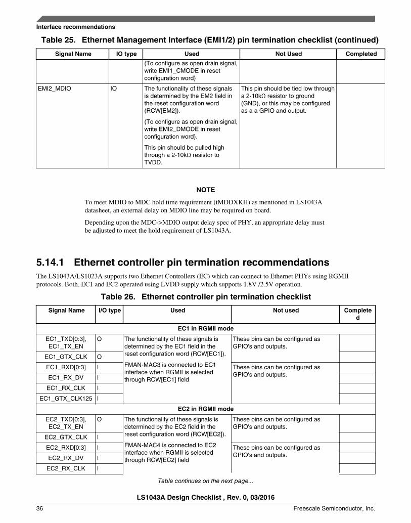
Table 25. Ethernet Management Interface (EMI1/2) pin termination checklist (continued)
Signal Name IO type Used Not Used Completed
(To configure as open drain signal,write EMI1_CMODE in resetconfiguration word)
EMI2_MDIO IO The functionality of these signalsis determined by the EM2 field inthe reset configuration word(RCW[EM2]).
(To configure as open drain signal,write EMI2_DMODE in resetconfiguration word).
This pin should be pulled highthrough a 2-10kΩ resistor toTVDD.
This pin should be tied low througha 2-10kΩ resistor to ground(GND), or this may be configuredas a a GPIO and output.
NOTE
To meet MDIO to MDC hold time requirement (tMDDXKH) as mentioned in LS1043Adatasheet, an external delay on MDIO line may be required on board.
Depending upon the MDC->MDIO output delay spec of PHY, an appropriate delay mustbe adjusted to meet the hold requirement of LS1043A.
5.14.1 Ethernet controller pin termination recommendationsThe LS1043A/LS1023A supports two Ethernet Controllers (EC) which can connect to Ethernet PHYs using RGMIIprotocols. Both, EC1 and EC2 operated using LVDD supply which supports 1.8V /2.5V operation.
Table 26. Ethernet controller pin termination checklist
Signal Name I/O type Used Not used Completed
EC1 in RGMII mode
EC1_TXD[0:3],EC1_TX_EN
O The functionality of these signals isdetermined by the EC1 field in thereset configuration word (RCW[EC1]).
FMAN-MAC3 is connected to EC1interface when RGMII is selectedthrough RCW[EC1] field
These pins can be configured asGPIO's and outputs.
EC1_GTX_CLK O
EC1_RXD[0:3] I These pins can be configured asGPIO's and outputs.EC1_RX_DV I
EC1_RX_CLK I
EC1_GTX_CLK125 I
EC2 in RGMII mode
EC2_TXD[0:3],EC2_TX_EN
O The functionality of these signals isdetermined by the EC2 field in thereset configuration word (RCW[EC2]).
FMAN-MAC4 is connected to EC2interface when RGMII is selectedthrough RCW[EC2] field
These pins can be configured asGPIO's and outputs.
EC2_GTX_CLK I
EC2_RXD[0:3] I These pins can be configured asGPIO's and outputs.EC2_RX_DV I
EC2_RX_CLK I
Table continues on the next page...
Interface recommendations
LS1043A Design Checklist , Rev. 0, 03/2016
36 Freescale Semiconductor, Inc.

Table 26. Ethernet controller pin termination checklist (continued)
Signal Name I/O type Used Not used Completed
EC2_GTX_CLK125 I
5.15 QUICC Engine recommendationsQUICC Engine Block in LS1043/LS1023 supports two TDM/HDLC interfaces.
The functionality of these signals is determined by the QE-TDMA and QE-TDMB fields in the reset configuration word.
QUICC Engine supports 3.3V and 1.8V operation only
5.15.1 QUICC Engine pin termination recommendations
Table 27. QUICC Engine pin termination checklist
Signal Name I/O type Used Not used Completed
QE Clock Signals
BRGO[1 & 4] O The functionality of BRGO1 andBRGO4 signals is determined by theIIC3_SDA and IIC3_SCL respectivelyin SCFG_RCWPMUXCR0 register.
Similarly CLK12 and CLK11 signalsis determined by the IIC3_SDA andIIC3_SCL respectively inSCFG_RCWPMUXCR0 register.
Program as GPIOs and as output.
CLK[11:12] I
BRGO[2:3] O The functionality of this signal isdetermined by the RCW[IIC2_EXT]fields in reset configuration word.
RCW[QE_CLK_OVRRIDE] field inreset configuration word providesoptions to select other combinationsof BRGs and CLKs. Please refer toreference manual for more details.
Program as GPIOs and as output.
CLK[9:10] I
UCC1 signals
UC1_CDB_RXER I The functionality of these signals isdetermined by the RCW[IRQ_EXT]field in the reset configuration wordexcept for UC1_CDB_RXER which isdetermined by the IIC4_SCL bitfieldin register SCFG_RCWPMUXCR0
If UCC1 is not used, all the pins canbe programmed as GPIO's andoutputs.
UC1_CTSB_RXDV I
UC1_RXD7 I
UC1_TXD7 O
UC1_RTSB_TXEN O
UCC3 signals
Table continues on the next page...
Interface recommendations
LS1043A Design Checklist , Rev. 0, 03/2016
Freescale Semiconductor, Inc. 37

Table 27. QUICC Engine pin termination checklist (continued)
Signal Name I/O type Used Not used Completed
UC3_CDB_RXER I The functionality of these signals isdetermined by the RCW[IRQ_EXT]field in the reset configuration wordexcept for UC3_CDB_RXER which isdetermined by the IIC4_SDA bitfieldin register SCFG_RCWPMUXCR0
If UCC3 is not used, all the pins canbe programmed as GPIO's andoutputs.
UC3_CTSB_RXDV I
UC3_RXD7 I
UC3_TXD7 O
UC3_RTSB_TXEN O
TDMA signals
TDMA_TXD O The functionality of these signals isdetermined by the RCW[IRQ_EXT]field in the reset configuration wordexcept for TDMA_RQ which isdetermined by the IIC4_SCL bitfieldin register SCFG_RCWPMUXCR0
If TDMA is not used, all the pins canbe programmed as GPIO's andoutputs.
TDMA_TSYNC I
TDMA_RQ O
TDMA_RSYNC I
TDMA_RXD I
TDMB signals
TDMB_TXD O The functionality of these signals isdetermined by the RCW[IRQ_EXT]field in the reset configuration wordexcept for TDMB_RQ which isdetermined by the IIC4_SDA bitfieldin register SCFG_RCWPMUXCR0
If TDMB is not used, all the pins canbe programmed as GPIO's andoutputs.
TDMB_TSYNC I
TDMB_RQ O
TDMB_RSYNC I
TDMB_RXD I
Strobe signals
QE_SI1_STROBE[0:1] O The functionality of these signals isdetermined by the RCW[IIC2_EXT]field in the reset configuration word.
If Strobes are not used, all the pinscan be programmed as GPIO's andoutputs.
5.16 QSPI pin termination recommendationsTable 28. QSPI pin termination checklist
Signal Name IO type Used Not Used Completed
QSPI_A_SCK O The functionality of these signals isdetermined by theRCW[IFC_GRP_F_EXT] bits ofreset configuration word.
Pin can be left unconnected.
QSPI_B_SCK O The functionality of these signals isdetermined by theRCW[IFC_GRP_F_EXT] bits ofreset configuration word.
Pin can be left unconnected
QSPI_A_CS[0:1] O The functionality of these signals isdetermined by theRCW[IFC_GRP_F_EXT] bits ofreset configuration word.
Pin can be left unconnected
Table continues on the next page...
Interface recommendations
LS1043A Design Checklist , Rev. 0, 03/2016
38 Freescale Semiconductor, Inc.

Table 28. QSPI pin termination checklist (continued)
Signal Name IO type Used Not Used Completed
QSPI_B_CS[0:1] O The functionality of these signals isdetermined by theRCW[IFC_GRP_F_EXT] bits ofreset configuration word.
Pin can be left unconnected
QSPI_A_DATA[0:2] IO The functionality of these signals isdetermined by theRCW[IFC_GRP_F_EXT] bits ofreset configuration word.
If this pin is not used, it should beprogrammed as GPIO and output.
QSPI_A_DATA[3] IO The functionality of these signals isdetermined by theRCW[IFC_GRP_A_EXT] bits ofreset configuration word.
If this pin is not used, it should beprogrammed as GPIO and output.
QSPI_B_DATA[0:2] IO The functionality of these signals isdetermined by theRCW[IFC_GRP_D_EXT] bits ofreset configuration word.
If this pin is not used, it should beprogrammed as GPIO and output.
QSPI_B_DATA[3] IO The functionality of these signals isdetermined by theRCW[IFC_GRP_E1_EXT] bits ofreset configuration word.
If this pin is not used, it should beprogrammed as GPIO and output.
5.17 SPI recommendationsThe LS1043A/LS1023A serial peripheral interface (SPI) pins are powered from OVDD supply, which supports 1.8V only.
5.17.1 SPI pin termination recommendationsTable 29. SPI pin termination checklist
Signal name I/O type Used Not used Completed
SPI_MISO I The functionality of this signal isdetermined by the SPI_BASE andSPI_EXT field in the reset configuration(RCW[SPI_EXT]).
This pin should be pulled high through a2-10 kΩ resistor to OVDD.
SPI_MOSI I/O The functionality of this signal isdetermined by the SPI_BASE andSPI_EXT field in the reset configuration(RCW[SPI_EXT]).
This pin should be pulled high through a2-10 kΩ resistor to OVDD.
SPI_CLK O The functionality of this signal isdetermined by the SPI_BASE andSPI_EXT field in the reset configuration(RCW[SPI_EXT]).
This pin may be left unconnected.
SPI_CS[0:3]_B O The functionality of this signal isdetermined by the SPI_BASE field inthe reset configuration(RCW[SPI_BASE]).
These pins may be left unconnected.
Interface recommendations
LS1043A Design Checklist , Rev. 0, 03/2016
Freescale Semiconductor, Inc. 39

5.18 General Purpose Input/Output pin terminationrecommendations
Table 30. General Purpose Input/Output pin termination checklist
Signal Name IO type Used Not Used Completed
GPIO1_13 IO The functionality of this signal isdetermined by the RCW[ASLEEP]field in the reset configurationword.
For all GPIOx pins: Whenprogrammed as outputs, notermination is required.
GPIO1_14 IO The functionality of this signal isdetermined by the RCW[RTC] fieldin the reset configuration word.
GPIO1_[15:22] IO The functionality of these signalsis determined by theRCW[UART_BASE] &RCW[UART_EXT] field in thereset configuration word.
GPIO1_[23:31] IO The functionality of these signalsis determined by theRCW[IRQ_EXT] andRCW[IRQ_BASE] fields in thereset configuration word.
GPIO2_[0:3] IO The functionality of these signalsis determined by theRCW[SPI_BASE] fields in thereset configuration word.
For all GPIOx pins: Whenprogrammed as outputs, notermination is required.
GPIO2_[4:9] IO The functionality of these signalsis determined by theRCW[SDHC_BASE] fields in thereset configuration word.
For all GPIOx pins: Whenprogrammed as outputs, notermination is required.
GPIO2_[10:12] IO The functionality of these signalsis determined by theRCW[IFC_GRP_E1_BASE] field inthe reset configuration word.
For all GPIOx pins: Whenprogrammed as outputs, notermination is required.
GPIO2_[13:15] IO The functionality of these signalsis determined by theRCW[IFC_GRP_D_BASE] fields inthe reset configuration word.
GPIO2_[25:27] IO The functionality of these signalsis determined by theRCW[IFC_GRP_A_BASE] field inthe reset configuration word.
GPIO3_[0:1] IO The functionality of these signalsis determined by the RCW[EM1]field in the reset configurationword.
For all GPIOx pins: Whenprogrammed as outputs, notermination is required.
Table continues on the next page...
Interface recommendations
LS1043A Design Checklist , Rev. 0, 03/2016
40 Freescale Semiconductor, Inc.

Table 30. General Purpose Input/Output pin termination checklist (continued)
Signal Name IO type Used Not Used Completed
GPIO3_[2:14] IO The functionality of these signalsis determined by the RCW[EC1]field in the reset configurationword.
GPIO3_[15:27] IO The functionality of these signalsis determined by the RCW[EC2]field in the reset configurationword.
GPIO4_[0:1] IO The functionality of these signalsis determined by the RCW[EM2]field in the reset configurationword.
For all GPIOx pins: Whenprogrammed as outputs, notermination is required.
GPIO4_[2:3] IO The functionality of these signalsis determined by theRCW[IIC2_EXT] field in the resetconfiguration word.
GPIO4_[10:11] IO The functionality of these signalsis determined by the IIC3_SCLand IIC3_SDA fields inSCFG_RCWPMUXCR0respectively.
GPIO4_[12:13] IO The functionality of these signalsis determined by the IIC4_SCLand IIC4_SDA fields inSCFG_RCWPMUXCR0respectively.
GPIO4_[29] IO The functionality of these signalsis determined by theRCW[USB_DRVVBUS] field in thereset configuration word.
GPIO4_[30] IO The functionality of these signalsis determined by theRCW[USB_PWRFAULT] fields inthe reset configuration word.
For all GPIOx pins: Whenprogrammed as outputs, notermination is required.
5.19 FTM1 pin termination recommendationsTable 31. FTM1 pin termination checklist
Signal Name IO type Used Not Used Completed
FTM1_CH[0:7] IO The functionality of this signal isdetermined by the EC1 field in thereset configuration (RCW[EC1]).
Program as GPIOs and asoutputs.
FTM1_EXTCLK I The functionality of this signal isdetermined by the EC1 field in thereset configuration (RCW[EC1]).
Program as GPIOs and asoutputs.
Table continues on the next page...
Interface recommendations
LS1043A Design Checklist , Rev. 0, 03/2016
Freescale Semiconductor, Inc. 41

Table 31. FTM1 pin termination checklist (continued)
Signal Name IO type Used Not Used Completed
FTM1_FAULT I The functionality of this signal isdetermined by the EC1 field in thereset configuration (RCW[EC1]).
Program as GPIOs and asoutputs.
FTM1_QD_PHA I The functionality of this signal isdetermined by the EC1 field in thereset configuration (RCW[EC1]).
Program as GPIOs and asoutputs.
FTM1_QD_PHB I The functionality of this signal isdetermined by the EC1 field in thereset configuration (RCW[EC1]).
Program as GPIOs and asoutputs.
5.20 FTM2 pin termination recommendationsTable 32. FTM2 pin termination checklist
Signal Name IO type Used Not Used Completed
FTM2_CH[0:7] IO The functionality of this signal isdetermined by the EC2 field in thereset configuration (RCW[EC2]).
Program as a GPIO and as anoutput.
FTM2_EXTCLK I The functionality of this signal isdetermined by the EC2 field in thereset configuration (RCW[EC2]).
Program as a GPIO and as anoutput.
FTM2_FAULT I The functionality of this signal isdetermined by the EC2 field in thereset configuration (RCW[EC2]).
Program as a GPIO and as anoutput.
FTM2_QD_PHA I The functionality of this signal isdetermined by the EC2 field in thereset configuration (RCW[EC2]).
Program as a GPIO and as anoutput.
FTM2_QD_PHB I The functionality of this signal isdetermined by the EC2 field in thereset configuration (RCW[EC2]).
Program as a GPIO and as anoutput.
5.21 FTM3 pin termination recommendationsTable 33. FTM3 pin termination checklist
Signal Name IO type Used Not Used Completed
FTM3_CH[0:7] IO The functionality of these signalsis determined by the IRQ_BASEand IRQ_EXT fields in the resetconfiguration word(RCW[IRQ_BASE] andRCW[IRQ_EXT]).
Program as a GPIO and as anoutput.
Table continues on the next page...
Interface recommendations
LS1043A Design Checklist , Rev. 0, 03/2016
42 Freescale Semiconductor, Inc.

Table 33. FTM3 pin termination checklist (continued)
Signal Name IO type Used Not Used Completed
FTM3_EXTCLK I The functionality of these signalsis determined by the IIC4_SDAbitfield in registerSCFG_RCWPMUXCR0
Program as a GPIO and as anoutput.
FTM3_FAULT I The functionality of these signalsis determined by the IIC4_SCLbitfield in registerSCFG_RCWPMUXCR0
Program as a GPIO and as anoutput.
FTM3_QD_PHA I The functionality of these signalsis determined by the IIC2_EXTfields in the reset configurationword (RCW[IIC2_EXT]).
Program as a GPIO and as anoutput.
FTM3_QD_PHB I The functionality of these signalsis determined by the IIC2_EXTfields in the reset configurationword (RCW[IIC2_EXT]).
Program as a GPIO and as anoutput.
5.22 FTM4 pin termination recommendationsTable 34. FTM4 pin termination checklist
Signal Name IO type Used Not Used Completed
FTM4_CH[0:7] IO he functionality of FTM4_CH[0-5]signals is determined by theUART_EXT fields in the resetconfiguration word(RCW[UART_EXT]).
The functionality of FTM4_CH6and FTM4_CH7 signals isdetermined by the SDHC_EXTfields in the reset configurationword (RCW[SDHC_EXT]).
Program as a GPIO and as anoutput.
FTM4_EXTCLK I The functionality of these signalsis determined by the SDHC_EXTfields in the reset configurationword (RCW[SDHC_EXT]).
Program as a GPIO and as anoutput.
FTM4_FAULT I The functionality of these signalsis determined by the SDHC_EXTfields in the reset configurationword (RCW[SDHC_EXT]).
Program as a GPIO and as anoutput.
FTM4_QD_PHA I The functionality of these signalsis determined by the SDHC_EXTfields in the reset configurationword (RCW[SDHC_EXT]).
Program as a GPIO and as anoutput.
FTM4_QD_PHB I The functionality of these signalsis determined by the SDHC_EXTfields in the reset configurationword (RCW[SDHC_EXT]).
Program as a GPIO and as anoutput.
Interface recommendations
LS1043A Design Checklist , Rev. 0, 03/2016
Freescale Semiconductor, Inc. 43

5.23 FTM5 pin termination recommendationsTable 35. FTM5 pin termination checklist
Signal Name IO type Used Not Used Completed
FTM5_CH[0:1] IO The functionality of these signalsis determined by theIFC_GRP_A_EXT fields in thereset configuration word(RCW[IFC_GRP_A_EXT]).
Program as a GPIO and as anoutput.
FTM5_EXTCLK I The functionality of these signalsis determined by theIFC_GRP_A_EXT fields in thereset configuration word(RCW[IFC_GRP_A_EXT]).
Program as a GPIO and as anoutput.
5.24 FTM6 pin termination recommendationsTable 36. FTM6 pin termination checklist
Signal Name IO type Used Not Used Completed
FTM6_CH[0:1] IO The functionality of these signalsis determined by theIFC_GRP_D_EXT fields in thereset configuration word(RCW[IFC_GRP_D_EXT]).
Program as a GPIO and as anoutput.
FTM6_EXTCLK I The functionality of these signalsis determined by theIFC_GRP_D_EXT fields in thereset configuration word(RCW[IFC_GRP_D_EXT]).
Program as a GPIO and as anoutput.
5.25 FTM7 pin termination recommendationsTable 37. FTM7 pin termination checklist
Signal Name IO type Used Not Used Completed
FTM7_CH[0:1] IO The functionality of these signalsis determined by theIFC_GRP_E1_EXT fields in thereset configuration word(RCW[IFC_GRP_E1_EXT]).
Program as a GPIO and as anoutput.
Table continues on the next page...
Interface recommendations
LS1043A Design Checklist , Rev. 0, 03/2016
44 Freescale Semiconductor, Inc.

Table 37. FTM7 pin termination checklist (continued)
Signal Name IO type Used Not Used Completed
FTM7_EXTCLK I The functionality of these signalsis determined by theIFC_GRP_E1_EXT fields in thereset configuration word(RCW[IFC_GRP_E1_EXT]).
Program as a GPIO and as anoutput.
5.26 FTM8 pin termination recommendationsTable 38. FTM8 pin termination checklist
Signal Name IO type Used Not Used Completed
FTM8_CH[0:1] IO The functionality of these signalsis determined by the IIC3_SCLand IIC3_SDA bitfieldsrespectively in registerSCFG_RCWPMUXCR0
Program as a GPIO and as anoutput.
5.27 IEEE1588 recommendations
5.27.1 IEEE 1588 pin termination recommendationsTable 39. IEEE 1588 pin termination checklist
Signal Name I/O type Used Not used Completed
TSEC_1588_CLK_IN I Connect to external high-precisiontimer reference input.
The functionality of these signals isdetermined by the EC2 field in thereset configuration word(RCW[EC2]).
Program as GPIO's and output.
TSEC_1588_ALARM_OUT1
O The functionality of these signals isdetermined by the EC2 field in thereset configuration word(RCW[EC2]).
Program as GPIO's and output.
TSEC_1588_ALARM_OUT2
O The functionality of these signals isdetermined by the EC2 field in thereset configuration word(RCW[EC2]).
Program as GPIO's and output.
TSEC_1588_CLK_OUT
O The functionality of these signals isdetermined by the EC2 field in the
Program as GPIO's and output.
Table continues on the next page...
Interface recommendations
LS1043A Design Checklist , Rev. 0, 03/2016
Freescale Semiconductor, Inc. 45

Table 39. IEEE 1588 pin termination checklist (continued)
Signal Name I/O type Used Not used Completed
reset configuration word(RCW[EC2]).
TSEC_1588_PULSE_OUT1
O The functionality of these signals isdetermined by the EC2 field in thereset configuration word(RCW[EC2]).
Program as GPIO's and output.
TSEC_1588_PULSE_OUT2
O The functionality of these signals isdetermined by the EC2 field in thereset configuration word(RCW[EC2]).
Program as GPIO's and output.
TSEC_1588_TRIG_IN1
I The functionality of these signals isdetermined by the EC2 field in thereset configuration word(RCW[EC2]).
Program as GPIO's and output.
TSEC_1588_TRIG_IN2
I The functionality of these signals isdetermined by the EC2 field in thereset configuration word(RCW[EC2]).
Program as GPIO's and output.
NOTE1. When configured for IEEE1588, the EC2 pins those are not available for
IEEE1588, are configured for GPIO. All IEEE 1588 pins are referenced to LVDD.
5.28 System control pin termination recommendationsTable 40. System Control pin termination checklist
Signal Name I/O type Used Not used Completed
PORESET_B I This pin is required to be asserted as per the applicable chip data sheet, inrelation to minimum assertion time and during power-up/power-down. It is aninput-only pin and must be asserted to sample power on configuration pins.
HRESET_B I/O This pin is an open drain signal and should be pulled high through a 2-10 kΩresistor to OVDD.
RESET_REQ_B O Must not be pulled down during power-on reset.
This pin should be pulled high througha 2-10 kΩ resistor to OVDD and mustnot be pulled down during power-onreset.
NOTE1. If on-board programming of NOR and NAND boot flash, QSPI boot flash, or SD
card is needed, then maintain an option (may be via a jumper) that keepsPORESET_B and RESET_REQ_B disconnected from each other. Booting from ablank NAND flash or SPI flash causes boot error, which in turn causes assertion ofRESET_REQ_B. When RESET_REQ_B is connected with PORESET_B, thedevice goes in a recurring reset loop and does not provide enough time for JTAG totake control of the device and perform any operation.
Interface recommendations
LS1043A Design Checklist , Rev. 0, 03/2016
46 Freescale Semiconductor, Inc.

2. For RCW override, RESET_REQ_B should be disconnected from PORESET_B orHRESET_B. An option on board is required.
5.29 JTAG pin termination recommendationsTable 41. JTAG pin termination checklist
Signal Name IO type Used Not Used Completed
TCK I Connect to pin 4 of the ARM Cortex 10-pin header. This pin requires a2-10kΩ resistor to OVDD.
TDI I Connect to pin 8 of the ARMCortex 10-pin header. This pin hasa weak (~20 kΩ) internal pull-up P-FET that is always enabled.
May be left unconnected.
TDO O Connect to pin 6 of the ARMCortex 10-pin header. This outputis actively driven during resetrather than being tri-stated duringreset.
May be left unconnected.
TMS I Connect to pin 2 of the ARMCortex 10-pin header. This pin hasa weak (~20 kΩ) internal pull-up P-FET that is always enabled.
May be left unconnected.
TRST_B I This pin has a weak (~20 kΩ)internal pull-up P-FET that isalways enabled.
Connect as shown in Figure 11.
Tie TRST_B to PORESET_Bthrough a 0 kΩ resistor.
5.29.1 JTAG system-level recommendationsTable 42. JTAG system-level checklist
Item Completed
ARM®Cortex® 10-pin header signal interface to JTAG port
Configure the group of system control pins as shown in Figure 11.
NOTE: These pins must be maintained at a valid deasserted state under normal operating conditions,because most have asynchronous behavior and spurious assertion gives unpredictable results.
The JTAG port of these processors allows a remote computer system (typically, a PC with dedicated hardwareand debugging software) to access and control the internal operations of the processor. The ARM Cortex 10-pin header connects primarily through the JTAG port of the processor, with some additional status monitoringsignals. The ARM Cortex 10-pin header interface requires the ability to independently assert PORESET_B inorder to fully control the processor. If the target system has independent reset sources, such as voltagemonitors, watchdog timers, power supply failures, or push-button switches, then the nRESET signals must bemerged into these signals with logic.
Boundary-scan testing
Ensure that TRST_B is asserted during power-on reset flow to ensure that the JTAG boundary logic does notinterfere with normal chip operation.
Table continues on the next page...
Interface recommendations
LS1043A Design Checklist , Rev. 0, 03/2016
Freescale Semiconductor, Inc. 47

Table 42. JTAG system-level checklist (continued)
Item Completed
Follow the arrangement shown in Figure 11 to allow the ARM Cortex 10-pin header to assert PORESET_Bindependently while ensuring that the target can drive PORESET_B as well.
The ARM® Cortex® 10-pin interface has a standard header, shown in the following figure. The connectortypically has pin 7 removed as a connector key. The signal placement recommended in this figure is commonto all known emulators.
1 2
3
5
9
4
6
8
10
KEYNo pin
VDD
GND
GND
KEY
GNDDetect
TMS
nRESET
TCK
TDO
TDI
NOTE: The ARM Cortex 10-pin header adds many benefits such as breakpoints, watch points, register andmemory examination/modification, and other standard debugger features. An inexpensive option is toleave the ARM Cortex 10-pin header unpopulated until needed.
Correct operation of the JTAG interface requires configuration of a group of system control pins as demonstrated in Figure11. Care must be taken to ensure that these pins are maintained at a valid deasserted state under normal operating conditions,as most have asynchronous behavior and spurious assertion gives unpredictable results.
Interface recommendations
LS1043A Design Checklist , Rev. 0, 03/2016
48 Freescale Semiconductor, Inc.

1 2
3
5
9
4
6
8
10 2
1
10
VDD
10 kΩ
10 kΩ
1 kΩ
HRESET_B
PORESET_B
TMS
TDO
TDI
TCK
OVDD
HRESET_B
PORESET_B
From targetboard sources
(if any)
nRESET
10 Ω
KEYNo pin
TCK
TDI
TDO
TMS
AR
M C
ort
ex 1
0-p
in h
ead
er
10 kΩ
6
8
4
GNDDetect1
GND
GND9
5
3
ARM Cortex 10-pinphysical pinout
Note:1. GNDDetect is an optional board feature. Check with 3rd-party tool vendor.2. This switch is included as a precaution for BSDL testing. The switch should be open during BSDL testing to avoid accidentally asserting the TRST line. If BSDL testing is not being performed, ensure this switch is closed.
TRST_B
OVDD
10 kΩ
Other TRST_B source(for example, boundary scan)
10 kΩ
2
Figure 11. JTAG interface connection
Interface recommendations
LS1043A Design Checklist , Rev. 0, 03/2016
Freescale Semiconductor, Inc. 49

5.30 Clock pin termination recommendationsTable 43. Clock pin termination checklist
Signal Name IO type Used Not Used Completed
EC1_GTX_CLK O The functionality of this signal isdetermined by the EC1 field in thereset configuration word(RCW[EC1]).
LS1043A has a duty cyclereshaper inside RGMII block. Thisallows GTX clock from RGMII PHYto be used.
Program as a GPIO and as an output.
EC1_GTX_CLK125 I
EC2_GTX_CLK O The functionality of this signal isdetermined by the EC2 field in thereset configuration word(RCW[EC2]).
LS1043A has a duty cyclereshaper inside RGMII block. Thisallows GTX clock from RGMII PHYto be used.
Program as a GPIO and as an output.
EC2_GTX_CLK125 I
SYSCLK I This is the single-ended primaryclock input to the chip. It supportsa 64.0 MHz to 100.0 MHz clockrange.
Note that 64MHz SYSCLKreference frequency is specificallyfor Profibus support on QUICCEngine.
This pin should be pulled low through a2-10kΩ resistor to GND.1
DIFF_SYSCLK I These pins are the differentialprimary clock input to the chip.These pins support 100MHz only.When used, these pins should beconnected to a 100MHz differentialclock generator.
These pins should be pulled low througha 2-10kΩ resistor to GND, or they can beleft floating.3
DIFF_SYSCLK_B I
RTC I The functionality of this signal isdetermined by the RTC field in thereset configuration word(RCW[RTC]).
Pull low through a 2-10kΩ resistor toGND, or program pin as a GPIO andoutput.
DDRCLK I The reference clock for the DDRcontroller supports a 64 MHz to100 MHz input clock range.
This pin should be pulled low through a2-10kΩ resistor to GND.2, 4
NOTE1. In the "Single Oscillator Source" reference clock mode supported by LS1043A,
DIFF_SYSCLK/DIFF_SYSCLK_B (differential) clock inputs are used as primaryclock inputs and SYSCLK is unused. Power-on-configuration signal cfg_eng_use0selects between SYSCLK (single ended) and DIFF_SYSCLK/DIFF_SYSCLK_B(differential) clock inputs.
2. In the "Single Oscillator Source" reference clock mode, DIFF_SYSCLK/DIFF_SYSCLK_B clock inputs can be selected to feed the DDR PLL. RCW bits[DDR_REFCLK_SEL] are used for this selection and DDRCLK is unused.
Interface recommendations
LS1043A Design Checklist , Rev. 0, 03/2016
50 Freescale Semiconductor, Inc.

3. When SYSCLK is chosen as the primary clock input to the chip, these pins areunused.
4. The options for RCW bits 186-187 (DDR_REFCLK_SEL, DDR reference clockselection) are as follows:
00 The DDRCLK pin provides the reference clock to the DDR PLL
10 DIFF_SYSCLK/DIFF_SYSCLK_B provides the reference clock to the DDRPLL
5.31 Single Source ClockingThe chip supports the single source clocking options with single, two, and more reference clocks.
5.32 "Single Oscillator Source" Reference Clock ModeIn this mode, single onboard oscillator can provide the reference clock (100MHz) to the following PLLs:
• Platform PLL• Core PLLs• USB PLL• DDR PLL• SerDes PLLs
The reset configuration field identifies whether the SYSCLK (single-ended) or DIFF_SYSCLK (differential) is selected asthe clock input to the chip.
The RCW[DDR_REFCLK_SEL] bit is used to select clock input (DIFF_SYSCLK or DDRCLK) to the DDR PLL.
The following figure shows the system view of single oscillator source clocking. In this figure, the on-board oscillatorgenerates three differential clock outputs. The first differential output is used to provide the clock to system clock associatedPLLs and DDR PLL. However, the second and third differential outputs are used to provide clocks to SerDes PLLs.
A multiplexer between system clock and USBCLK is used to provide the USB PHY reference clock to the USB PLL. And,multiplexer between DIFF_SYSCLK/DIFF_SYSCLK_B inputs and DDRCLK is used to provide reference clock to the DDRPLL.
The duty cycle reshaper reshapes the 125 MHz ECn_GTX_CLK125 which is fed into frame manager for transmission asECn_GTX_CLK.
Interface recommendations
LS1043A Design Checklist , Rev. 0, 03/2016
Freescale Semiconductor, Inc. 51

DDRPLL
DDR Controller
RCW[MEM_PLL_RAT]RCW[MEM_PLL_CFG]
1G-1.6G
DDRCLK
Platform Clock
RCW[SYS_PLL_CFG]RCW[SYS_PLL_RAT]
USB PHY
usb phy clkUSBCLK
SerDes PLL1
SerDes PLL2
Core PLL
Platform PLL
SYSCLK
SYS_REF_CLK
MU
X
EC1_GTX_CLK125
EC2_GTX_CLK125
On Board Oscillator
MU
X
RCW[DDR_REFCLK_SEL]
MU
X
DIFF_SYSCLK_B/DIFF_SYSCLK
cfg_eng_use0
Duty Cycle
Reshaper
125MHz duty cycle corrected clockS
D1_
RE
F_C
LK1_
P/S
D1_
RE
F_C
LK1_
N
SD
1_R
EF
_CLK
2_P
/SD
1_R
EF
_CLK
2_N
RCW[MEM_PLL_SPD]
RCW[SYS_PLL_SPD]
MU
X
(SCFG_USB_REFCLK_SELCR[1-3])
RGMII1 TX CLK (125MHz)
RGMII2 TX CLK (125MHz)
400 MHZ
1.0 - 1.5 GHz
100 MHZ
3 Differential outputs
3 instances
Figure 12. Single Oscillator Source Clocking
5.33 "Single Oscillator Source" clock selectThe single oscillator source clock select input, described in this table, selects between SYSCLK (single ended) andDIFF_SYSCLK/DIFF_SYSCLK_B (differential) inputs.
Table 44. Single oscillator source clock select
Functional signals Reset configuration name Value (binary) Options
IFC_WE0_B
Default (1)
cfg_eng_use0 0 DIFF_SYSCLK/DIFF_SYSCLK_B(differential)
1 SYSCLK (single ended)
IFC_OE_B
Default (1)
cfg_eng_use1
On-chip LVDS termination mustNOT be enabled when external(off-chip) termination are active.
0 On-chip LVDS termination disabled
1 On-chip LVDS termination enabled
IFC_WP_B[0] cfg_eng_use2 Reserved Reserved
Interface recommendations
LS1043A Design Checklist , Rev. 0, 03/2016
52 Freescale Semiconductor, Inc.
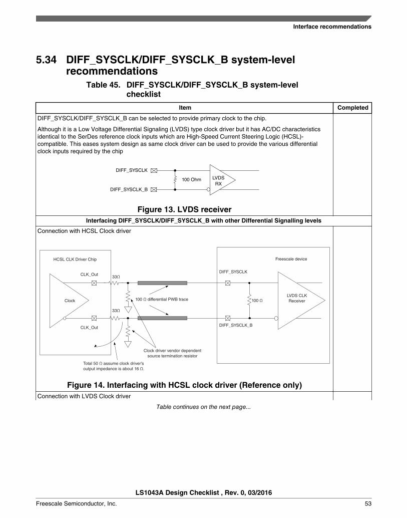
5.34 DIFF_SYSCLK/DIFF_SYSCLK_B system-levelrecommendations
Table 45. DIFF_SYSCLK/DIFF_SYSCLK_B system-levelchecklist
Item Completed
DIFF_SYSCLK/DIFF_SYSCLK_B can be selected to provide primary clock to the chip.
Although it is a Low Voltage Differential Signaling (LVDS) type clock driver but it has AC/DC characteristicsidentical to the SerDes reference clock inputs which are High-Speed Current Steering Logic (HCSL)-compatible. This eases system design as same clock driver can be used to provide the various differentialclock inputs required by the chip
DIFF_SYSCLK
DIFF_SYSCLK_B
100 Ohm LVDSRX
Figure 13. LVDS receiverInterfacing DIFF_SYSCLK/DIFF_SYSCLK_B with other Differential Signalling levels
Connection with HCSL Clock driver
HCSL CLK Driver Chip
CLK_Out
Clock
33Ω
100 Ω differential PWB trace
Total 50 Ω assume clock driver'soutput impedance is about 16 Ω.
Clock driver vendor dependentsource termination resistor
DIFF_SYSCLK
LVDS CLKReceiver
33Ω
CLK_Out
100 Ω
DIFF_SYSCLK_B
Freescale device
Figure 14. Interfacing with HCSL clock driver (Reference only)Connection with LVDS Clock driver
Table continues on the next page...
Interface recommendations
LS1043A Design Checklist , Rev. 0, 03/2016
Freescale Semiconductor, Inc. 53

Table 45. DIFF_SYSCLK/DIFF_SYSCLK_B system-level checklist(continued)
Item Completed
LVDS CLK Driver chip
CLK_Out
Clock 100 Ω differential PWB trace
DIFF_SYSCLK
LVDS CLKReceiver
CLK_Out
100 Ω
DIFF_SYSCLK_B
Freescale device
Figure 15. Interfacing with LVDS clock driver (Reference only)Connection with LVPECL Clock driver
LVPECL CLKDriver chip
CLK_Out
Clock 100 Ω differential PWB trace
DIFF_SYSCLK
LVDS CLKReceiver
R1
CLK_Out
100 Ω
DIFF_SYSCLK_B
Freescale device
R2
R2
R1
R1=140 Ω to 240 Ω
Figure 16. Interfacing with LVPECL clock driver (Reference only)Single-Ended Connection with Clock driver
The DIFF_SYSCLK_B should be terminated to OVDD/2
Interface recommendations
LS1043A Design Checklist , Rev. 0, 03/2016
54 Freescale Semiconductor, Inc.
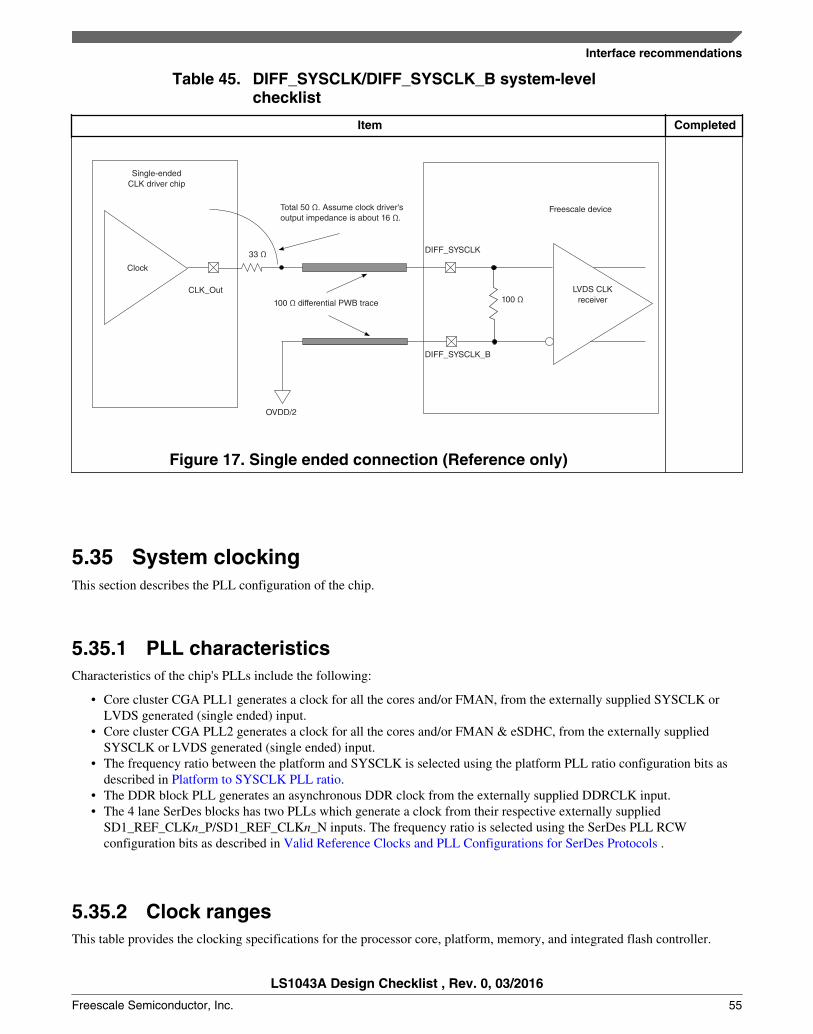
Table 45. DIFF_SYSCLK/DIFF_SYSCLK_B system-levelchecklist
Item Completed
Single-endedCLK driver chip
OVDD/2
Clock
100 Ω differential PWB trace
DIFF_SYSCLK
LVDS CLKreceiver
CLK_Out
DIFF_SYSCLK_B
Freescale device
100 Ω
33 Ω
Total 50 Ω. Assume clock driver'soutput impedance is about 16 Ω.
Figure 17. Single ended connection (Reference only)
5.35 System clockingThis section describes the PLL configuration of the chip.
5.35.1 PLL characteristicsCharacteristics of the chip's PLLs include the following:
• Core cluster CGA PLL1 generates a clock for all the cores and/or FMAN, from the externally supplied SYSCLK orLVDS generated (single ended) input.
• Core cluster CGA PLL2 generates a clock for all the cores and/or FMAN & eSDHC, from the externally suppliedSYSCLK or LVDS generated (single ended) input.
• The frequency ratio between the platform and SYSCLK is selected using the platform PLL ratio configuration bits asdescribed in Platform to SYSCLK PLL ratio.
• The DDR block PLL generates an asynchronous DDR clock from the externally supplied DDRCLK input.• The 4 lane SerDes blocks has two PLLs which generate a clock from their respective externally supplied
SD1_REF_CLKn_P/SD1_REF_CLKn_N inputs. The frequency ratio is selected using the SerDes PLL RCWconfiguration bits as described in Valid Reference Clocks and PLL Configurations for SerDes Protocols .
5.35.2 Clock rangesThis table provides the clocking specifications for the processor core, platform, memory, and integrated flash controller.
Interface recommendations
LS1043A Design Checklist , Rev. 0, 03/2016
Freescale Semiconductor, Inc. 55

Table 46. Processor, platform, and memory clocking specifications @ 1.0 V
Characteristic Maximum processor core frequency Unit Notes
1000 MHz 1200 MHz 1400 MHz 1600 MHz
Min Max Min Max Min Max Min Max
Core cluster group PLLfrequency
1000 1000 1000 1200 1000 1400 1000 1600 MHz 1
Platform clock frequency 256 300 256 300 256 300 256 400 MHz 1
Memory Bus Clock Frequency(DDR3L)
500 800 500 800 500 800 500 800 MHz 1, 2, 3
Memory Bus Clock Frequency(DDR4)
650 800 650 800 650 800 650 800 MHz 1, 3
IFC clock frequency - 100 - 100 - 100 - 100 MHz 4
FMan 350 500 350 500 350 500 350 500 MHz
1. Caution:The platform clock to SYSCLK ratio and core to SYSCLK ratio settings must be chosen such that the resultingSYSCLK frequency, core frequency, and platform clock frequency do not exceed their respective maximum or minimumoperating frequencies.
2. The memory bus clock speed is half the DDR3L/DDR4 data rate. DDR3L memory bus clock frequency is limited to min =1000 MT/s whereas DDR4 memory bus clock frequency is limited to min = 1300 MT/s.
3. The memory bus clock speed is dictated by its own PLL.
4. The integrated flash controller (IFC) clock speed on IFC_CLK[0:1] is determined by the IFC module input clock (platformclock / 2) divided by the IFC ratio programmed in CCR[CLKDIV]. See the chip reference manual for more information.
5. The minimum platform frequency should meet the requirements in Minimum platform frequency requirements for high-speed interfaces.
5.35.2.1 DDR clock rangesThe DDR memory controller can run only in asynchronous mode, where the memory bus is clocked with the clock providedon the DDRCLK input pin, which has its own dedicated PLL.
This table provides the clocking specifications for the memory bus.
Table 47. Memory bus clocking specifications @ 1.0 V
Characteristic Min Freq.(MHz) Max Freq.(MHz) Min Data Rate(MT/s)
Max Data Rate(MT/s)
Notes
Memory bus clockfrequency and DataRate for DDR3L
500 800 1000 1600 1, 2, 3
Memory bus clockfrequency and DataRate for DDR4
650 800 1300 1600 1, 2, 3
Notes:
1. Caution: The platform clock to SYSCLK ratio and core to platform clock ratio settings must be chosen such that theresulting SYSCLK frequency, core frequency, and platform frequency do not exceed their respective maximum or minimumoperating frequencies. See Platform to SYSCLK PLL ratio, and Core cluster to SYSCLK PLL ratio, and DDR controller PLLratios, for ratio settings.
Interface recommendations
LS1043A Design Checklist , Rev. 0, 03/2016
56 Freescale Semiconductor, Inc.

Table 47. Memory bus clocking specifications @ 1.0 V
Characteristic Min Freq.(MHz) Max Freq.(MHz) Min Data Rate(MT/s)
Max Data Rate(MT/s)
Notes
2. The memory bus clock refers to the chip's memory controllers' Dn_MCK[0:3] and Dn_MCK[0:3]_B output clocks, running athalf of the DDR data rate.
3. The memory bus clock speed is dictated by its own PLL. See DDR controller PLL ratios.
5.35.3 Platform to SYSCLK PLL ratioThis table lists the allowed platform clock to SYSCLK ratios.
Because the DDR operates asynchronously, the memory-bus clock-frequency is decoupled from the platform bus frequency.
For all valid platform frequencies supported on this chip, set the RCW Configuration field SYS_PLL_CFG = 0b00.
Table 48. Platform to SYSCLK PLL ratios @ 1.0 V
Binary Value of SYS_PLL_RAT Platform:SYSCLK Ratio
0_0011 3:1
0_0100 4:1
0_0101 5:1
0_0110 6:1
All Others Reserved
5.35.4 Core cluster to SYSCLK PLL ratioThe clock ratio between SYSCLK and each of the core cluster PLLs is determined by the binary value of the RCWConfiguration field CGm_PLLn_RAT. This table describes the supported ratios. For all valid core cluster frequenciessupported on this chip, set the RCW Configuration field CGn_PLL_CFG = 0b00.
This table below lists the supported asynchronous core cluster to SYSCLK ratios.
Table 49. Core cluster PLL to SYSCLK ratios @ 1.0 V
Binary value of CGm_PLLn_RAT Core cluster:SYSCLK Ratio
00_1010 10:1
00_1011 11:1
00_1100 12:1
00_1101 13:1
00_1110 14:1
00_1111 15:1
01_0000 16:1
01_0001 17:1
01_0010 18:1
Table continues on the next page...
Interface recommendations
LS1043A Design Checklist , Rev. 0, 03/2016
Freescale Semiconductor, Inc. 57

Table 49. Core cluster PLL to SYSCLK ratios @ 1.0 V(continued)
Binary value of CGm_PLLn_RAT Core cluster:SYSCLK Ratio
01_0011 19:1
01_0100 20:1
01_0101 21:1
01_0110 22:1
01_0111 23:1
01_1000 24:1
01_1001 25:1
All others Reserved
5.35.5 Core complex PLL selectThe clock frequency of each core is determined by the binary value of the RCW Configuration field C1_PLL_SEL. Thetables describe the selections available for each core, where each individual core can select a frequency from their respectivetables.
NOTEThere is a restriction that requires that the frequency provided to the ARM A53 core afterany dividers must always be greater than half of the platform frequency. Special caremust be used when selecting the /2 outputs of a cluster PLL in which this restriction isobserved.
Table 50. Core PLL select
Binary Value of C1_PLL_SEL Core cluster ratio
0000 CGA PLL1 /1
0001 CGA PLL1 /2
0100 CGA PLL2 /1
0101 CGA PLL2 /2
5.35.6 DDR controller PLL ratiosDDR memory controller operates asynchronous to the platform.
In asynchronous DDR mode, the DDR data rate to DDRCLK ratios supported are listed in the following table. This ratio isdetermined by the binary value of the RCW Configuration field MEM_PLL_RAT (bits 10-15).
The RCW Configuration field MEM_PLL_CFG (bits 8-9) must be set to MEM_PLL_CFG = 0b00 for all valid DDR PLLreference clock frequencies supported on this chip.
Interface recommendations
LS1043A Design Checklist , Rev. 0, 03/2016
58 Freescale Semiconductor, Inc.

Table 51. DDR clock ratio @ 1.0 V
Binary value of MEM_PLL_RAT DDR data-rate:DDRCLK
ratio
Maximum supported DDR data-rate (MT/s)
00_1010 10:1 The product of Input DDR Clock X Multiplication factorshould range between 1000 MHz-1600MHz.
00_1011 11:1 The product of Input DDR Clock X Multiplication factorshould range between 1000 MHz-1600MHz.
00_1100 12:1 The product of Input DDR Clock X Multiplication factorshould range between 1000 MHz-1600MHz.
00_1101 13:1 The product of Input DDR Clock X Multiplication factorshould range between 1000 MHz-1600MHz.
00_1110 14:1 The product of Input DDR Clock X Multiplication factorshould range between 1000 MHz-1600MHz.
00_1111 15:1 The product of Input DDR Clock X Multiplication factorshould range between 1000 MHz-1600MHz.
01_0000 16:1 The product of Input DDR Clock X Multiplication factorshould range between 1000 MHz-1600MHz.
01_0001 17:1 The product of Input DDR Clock X Multiplication factorshould range between 1000 MHz-1600MHz.
01_0010 18:1 The product of Input DDR Clock X Multiplication factorshould range between 1000 MHz-1600MHz.
01_0011 19:1 The product of Input DDR Clock X Multiplication factorshould range between 1000 MHz-1600MHz.
01_0100 20:1 The product of Input DDR Clock X Multiplication factorshould range between 1000 MHz-1600MHz.
01_0101 21:1 The product of Input DDR Clock X Multiplication factorshould range between 1000 MHz-1600MHz.
01_0110 22:1 The product of Input DDR Clock X Multiplication factorshould range between 1000 MHz-1600MHz.
01_0111 23:1 The product of Input DDR Clock X Multiplication factorshould range between 1000 MHz-1600MHz.
01_1000 24:1 The product of Input DDR Clock X Multiplication factorshould range between 1000 MHz-1600MHz.
All Others Reserved -
5.35.7 Valid Reference Clocks and PLL Configurations for SerDesProtocols
Each supported SerDes protocol allows for a finite set of valid SerDes-related RCW fields and reference clock frequencies.
The clock ratio between each SerDes PLLs and their respective externally supplied SD1_REF_CLKn_P/SD1_REF_CLKn_Ninputs is determined by a set of RCW Configuration fields-SRDS_PRTCL_S1, SRDS_PLL_REF_CLK_SEL_S1, andSRDS_DIV_* as shown in this table.
Interface recommendations
LS1043A Design Checklist , Rev. 0, 03/2016
Freescale Semiconductor, Inc. 59

Table 52. Valid SerDes RCW Encodings and Reference Clocks
SerDes protocol(given lane)
Valid referenceclock frequency
Valid
setting forSRDS_PRTCL_S1
Valid setting for SRDS_PLL_REF_CLK_SEL_S1
Valid
setting forSRDS_DIV_*_SnPLL1 PLL2
High Speed Serial interface
PCI Express 2.5Gbps (doesn'tnegotiate upwards)
100 MHz Any PCIe 0: 100 MHz 0: 100 MHz 10: 2.5G
125 MHz 1: 125 MHz 1: 125 MHz
PCI Express 5Gbps (cannegotiate up to 5Gbps)
100 MHz Any PCIe 0: 100 MHz 0: 100 MHz 01: 5G
125 MHz 1: 125 MHz 1: 125 MHz
SATA (1.5, 3, 6Gbps)
100 MHz Any SATA 0: 100 MHz - Don't Care
125 MHz 1: 125 MHz -
Networking interfaces
SGMII (1.25 Gbps) 100 MHz SGMII @ 1.25Gbps
0: 100 MHz 0: 100 MHz Don't Care
125 MHz 1: 125 MHz 1: 125 MHz
2.5 G SGMII (3.125Gbps)
125 Mhz SGMII @ 3.125Gbps
0: 125 MHz - Don't Care
156.25 MHz 1: 156.25 MHz -
QSGMII (5 Gbps) 100 MHz Any QSGMII 0: 100 MHz 0: 100 MHz Don't Care
125 MHz 1: 125 MHz 1: 125 MHz
XFI (10.3125 Gbps) 156.25 Mhz1: 156.25 MHz
- -
-
Notes:
1) A spread-spectrum reference clock is permitted for PCI Express. However, if any other high speed interface such asSGMII, QSGMII, SATA, or Debug is used concurrently on the same SerDes bank, spread-spectrum clocking is not permitted.
2) SerDes lanes configured as SATA initially operate at 3.0Gbps. 1.5Gbps operation may later be enabled through the SATAIP itself. It is possible for software to set each SATA at different rates.
5.35.8 Frequency optionsThis section discusses interface frequency options.
5.35.8.1 SYSCLK and core cluster frequency optionsThis table shows the expected frequency options for SYSCLK and core cluster frequencies.
Table 53. SYSCLK and core cluster frequency @ 1.0 V1
Core cluster: SYSCLK Ratio SYSCLK (MHz)
64.00 66.67 100.00
Core cluster Frequency - (MHz)1
10:1 1000
Table continues on the next page...
Interface recommendations
LS1043A Design Checklist , Rev. 0, 03/2016
60 Freescale Semiconductor, Inc.

Table 53. SYSCLK and core cluster frequency @ 1.0 V1 (continued)
Core cluster: SYSCLK Ratio SYSCLK (MHz)
64.00 66.67 100.00
Core cluster Frequency - (MHz)1
11:1 1100
12:1 1200
13:1 1300
14:1 1400
15:1 1000 1500
16:1 1024 1067 1600
17:1 1088 1133
18:1 1152 1200
19:1 1216 1267
20:1 1280 1333
21:1 1344 1400
22:1 1408 1467
23:1 1472 1533
24:1 1536 1600
25:1 1600
Notes:
1. Core cluster output is the operating frequency of the core.
2. Core cluster frequency values are shown rounded up to the nearest whole number (decimal place accuracy removed)
3. When using Single Source clocking only 100MHz input is available.
5.35.8.2 SYSCLK and platform frequency optionsThis table shows the expected frequency options for SYSCLK and platform frequencies.
Table 54. SYSCLK and platform frequency options @ 1.0 V
Platform: SYSCLK Ratio SYSCLK (MHz)
64.00 66.67 100.00
Platform Frequency (MHz)1
3:1 300
4:1 256 267 400
5:1 320 333
6:1 384 400
Notes:
1. Platform frequency values are shown rounded down to the nearest whole number (decimal place accuracy removed)
2. When using Single source clocking, only 100MHz options are valid
Interface recommendations
LS1043A Design Checklist , Rev. 0, 03/2016
Freescale Semiconductor, Inc. 61
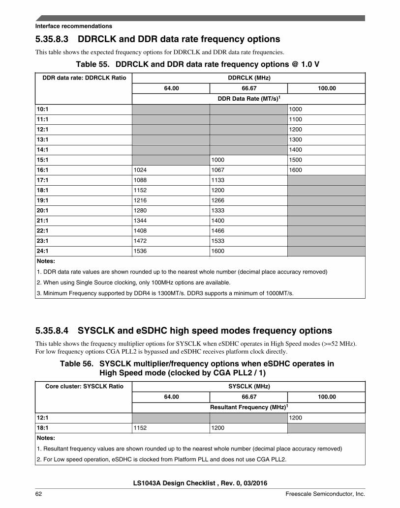
5.35.8.3 DDRCLK and DDR data rate frequency optionsThis table shows the expected frequency options for DDRCLK and DDR data rate frequencies.
Table 55. DDRCLK and DDR data rate frequency options @ 1.0 V
DDR data rate: DDRCLK Ratio DDRCLK (MHz)
64.00 66.67 100.00
DDR Data Rate (MT/s)1
10:1 1000
11:1 1100
12:1 1200
13:1 1300
14:1 1400
15:1 1000 1500
16:1 1024 1067 1600
17:1 1088 1133
18:1 1152 1200
19:1 1216 1266
20:1 1280 1333
21:1 1344 1400
22:1 1408 1466
23:1 1472 1533
24:1 1536 1600
Notes:
1. DDR data rate values are shown rounded up to the nearest whole number (decimal place accuracy removed)
2. When using Single Source clocking, only 100MHz options are available.
3. Minimum Frequency supported by DDR4 is 1300MT/s. DDR3 supports a minimum of 1000MT/s.
5.35.8.4 SYSCLK and eSDHC high speed modes frequency optionsThis table shows the frequency multiplier options for SYSCLK when eSDHC operates in High Speed modes (>=52 MHz).For low frequency options CGA PLL2 is bypassed and eSDHC receives platform clock directly.
Table 56. SYSCLK multiplier/frequency options when eSDHC operates inHigh Speed mode (clocked by CGA PLL2 / 1)
Core cluster: SYSCLK Ratio SYSCLK (MHz)
64.00 66.67 100.00
Resultant Frequency (MHz)1
12:1 1200
18:1 1152 1200
Notes:
1. Resultant frequency values are shown rounded up to the nearest whole number (decimal place accuracy removed)
2. For Low speed operation, eSDHC is clocked from Platform PLL and does not use CGA PLL2.
Interface recommendations
LS1043A Design Checklist , Rev. 0, 03/2016
62 Freescale Semiconductor, Inc.

5.35.8.5 Minimum platform frequency requirements for high-speedinterfaces
The platform clock frequency must be considered for proper operation of high-speed interfaces as described below:.Forproper PCI Express operation, the platform clock frequency must be greater than or equal to:
527 MHz x (PCI Express link width)
16
Figure 18. Gen 1 PEX minimum platform frequency
527 MHz x (PCI Express link width)
8
Figure 19. Gen 2 PEX minimum platform frequency
See section "Link Width," in the chip reference manual for PCI Express interface width details. Note that "PCI Express linkwidth" in the above equation refers to the negotiated link width as the result of PCI Express link training, which may or maynot be the same as the link width POR selection. It refers to the widest port in use, not the combined width of the numberports in use.
6 ThermalThis section discusses the thermal model and management of the chip.
6.1 Recommended thermal modelInformation about Flotherm models of the package or thermal data not available in this document can be obtained from yourlocal Freescale sales office.
6.2 Temperature diodeThe chip has a temperature diode on the microprocessor that can be used in conjunction with other system temperaturemonitoring devices (such as Analog Devices, ADT7461A). These devices feature series resistance cancellation using 3current measurements, where up to 1.5kΩ of resistance can be automatically cancelled from the temperature result, allowingnoise filtering and a more accurate reading.
The following are the specifications of the chip's on-board temperature diode:
Operating range: 10 - 230μA
Ideality factor over 13.5 - 220 μA; Temperature range 80°C - 105°C: n = 1.004 ± 0.008
Thermal
LS1043A Design Checklist , Rev. 0, 03/2016
Freescale Semiconductor, Inc. 63

6.3 Thermal management informationThis section provides thermal management information for the flip-chip, plastic-ball, grid array (FC-PBGA) package for air-cooled applications. Proper thermal control design is primarily dependent on the system-level design-the heat sink, airflow,and thermal interface material.
The recommended attachment method to the heat sink is illustrated in Figure 20. The heat sink should be attached to theprinted-circuit board with the spring force centered over the die. This spring force should not exceed 15 pounds force (65Newton).
Heat sink
Heat sink clip
Adhesive or thermal interface material
Printed circuit-board
Die
FC-PBGA package (no lid)
Figure 20. Package exploded, cross-sectional view-FC-PBGA (no lid)
The system board designer can choose between several types of heat sinks to place on the device. There are severalcommercially-available thermal interfaces to choose from in the industry. Ultimately, the final selection of an appropriateheat sink depends on many factors, such as thermal performance at a given air velocity, spatial volume, mass, attachmentmethod, assembly, and cost.
6.3.1 Internal package conduction resistanceFor the package, the intrinsic internal conduction thermal resistance paths are as follows:
• The die junction-to-case thermal resistance• The die junction-to-board thermal resistance
This figure shows the primary heat transfer path for a package with an attached heat sink mounted to a printed-circuit board.
Thermal
LS1043A Design Checklist , Rev. 0, 03/2016
64 Freescale Semiconductor, Inc.

External resistance
External resistance
Internal resistance
(Note the internal versus external package resistance)
Radiation Convection
Radiation Convection
Heat sink
Thermal interface material
Die/Package
Die junction
Package/Solder balls
Printed-circuit board
Figure 21. Package with heat sink mounted to a printed-circuit board
The heat sink removes most of the heat from the device. Heat generated on the active side of the chip is conducted throughthe silicon and through the heat sink attach material (or thermal interface material), and finally to the heat sink. The junction-to-case thermal resistance is low enough that the heat sink attach material and heat sink thermal resistance are the dominantterms.
6.3.2 Thermal interface materialsA thermal interface material is required at the package-to-heat sink interface to minimize the thermal contact resistance. Theperformance of thermal interface materials improves with increasing contact pressure; this performance characteristic chart isgenerally provided by the thermal interface vendor. The recommended method of mounting heat sinks on the package is bymeans of a spring clip attachment to the printed-circuit board (see Figure 20).
The system board designer can choose among several types of commercially available thermal interface materials.
7 Revision historyThis table summarizes changes to this document.
Revision history
LS1043A Design Checklist , Rev. 0, 03/2016
Freescale Semiconductor, Inc. 65

Table 57. Revision history
Revision Date Change
0 03/2016 Initial release
Revision history
LS1043A Design Checklist , Rev. 0, 03/2016
66 Freescale Semiconductor, Inc.
How to Reach Us:
Home Page:freescale.com
Web Support:freescale.com/support
Information in this document is provided solely to enable system and
software implementers to use Freescale products. There are no express
or implied copyright licenses granted hereunder to design or fabricate
any integrated circuits based on the information in this document.
Freescale reserves the right to make changes without further notice to
any products herein. Freescale makes no warranty, representation, or
guarantee regarding the suitability of its products for any particular
purpose, nor does Freescale assume any liability arising out of the
application or use of any product or circuit, and specifically disclaims
any and all liability, including without limitation consequential or
incidental damages. “Typical” parameters that may be provided in
Freescale data sheets and/or specifications can and do vary in different
applications, and actual performance may vary over time. All operating
parameters, including “typicals,” must be validated for each customer
application by customer's technical experts. Freescale does not convey
any license under its patent rights nor the rights of others. Freescale
sells products pursuant to standard terms and conditions of sale, which
can be found at the following address: freescale.com/
SalesTermsandConditions.
Freescale, the Freescale logo, AltiVec, C-5, CodeTest, CodeWarrior,
ColdFire, ColdFire+, C-Ware, Energy Efficient Solutions logo, Kinetis,
mobileGT, PowerQUICC, Processor Expert, QorIQ, Qorivva, StarCore,
Symphony, and VortiQa are trademarks of Freescale Semiconductor,
Inc., Reg. U.S. Pat. & Tm. Off. Airfast, BeeKit, BeeStack, CoreNet,
Flexis, Layerscape, MagniV, MXC, Platform in a Package, QorIQ
Qonverge, QUICC Engine, Ready Play, SafeAssure, SafeAssure logo,
SMARTMOS, Tower, TurboLink, Vybrid, and Xtrinsic are trademarks of
Freescale Semiconductor, Inc. All other product or service names are
the property of their respective owners.
© 2016 Freescale Semiconductor, Inc.
Document Number AN5012Revision 0, 03/2016