lt3992 - monolithic dual tracking 3a step-down … nc vout1 nc bst1 cmpo1 cmpi1 fb1 nc fb2 cmpi2...
TRANSCRIPT
LT3992
13992fa
For more information www.linear.com/LT3992
Typical applicaTion
FeaTures
applicaTions
DescripTion
Monolithic Dual Tracking 3A Step-Down Switching Regulator
The LT®3992 is a dual current mode PWM step-down DC/DC converter with two internal 4.6A switches. Inde-pendent input voltage, shutdown, feedback, soft-start, UVLO current limit and comparator pins for each channel simplify complex power supply tracking and sequencing requirements.
To optimize efficiency and component size, both convert-ers have a programmable maximum current limit and are synchronized to either a common external clock input, or a resistor settable fixed 250kHz to 2MHz internal oscillator. A frequency divider is provided for channel 1 to further optimize component size. At all frequencies, a 180° phase relationship between channels is maintained, reducing volt-age ripple and component size. A clock output is available for synchronizing multiple regulators.
Minimum input to output voltage ratios are improved by allowing the switch to stay on through multiple clock cycles only switching off when the boost capacitor needs recharg-ing. Independent channel operation can be programmed using the SHDN pin. Disabling both converters reduces the total quiescent current to <10µA.L, LT, LTC, LTM, Linear Technology, the Linear logo and Burst Mode are registered trademarks of Linear Technology Corporation. All other trademarks are the property of their respective owners.
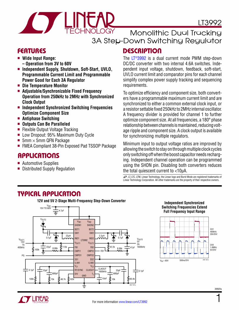
12V and 5V 2-Stage Multi-Frequency Step-Down Converter
n Wide Input Range: – Operation from 3V to 60Vn Independent Supply, Shutdown, Soft-Start, UVLO,
Programmable Current Limit and Programmable Power Good for Each 3A Regulator
n Die Temperature Monitorn Adjustable/Synchronizable Fixed Frequency
Operation from 250kHz to 2MHz with Synchronized Clock Output
n Independent Synchronized Switching Frequencies Optimize Component Size
n Antiphase Switching n Outputs Can Be Paralleledn Flexible Output Voltage Trackingn Low Dropout: 95% Maximum Duty Cyclen 5mm × 5mm QFN Packagen FMEA Compliant 38-Pin Exposed Pad TSSOP Package
n Automotive Suppliesn Distributed Supply Regulation
Independent Synchronized Switching Frequencies Extend
Full Frequency Input Range
BST1
SW1
VOUT1
CMPI1
CMPO1
SS1ILIM1
RT/SYNC
DIV
VC1
FB1
IND1
SW2
VOUT2
CMPI2
CMPO2
SS2ILIM2
CLKOUT
VC2
TJ
FB2
IND2
3992 TA01a
BST2
SHDN1 SHDN2
VIN1VOUT2
LT3992
GND
VIN2
4.7µF
VIN115V TO 60V
VOUT25V2A1600kHz
VOUT112V1A
400kHz100k
PG
22µH 2.2µH0.1µF 0.1µF
8.06k
102k15k100k
680pF33pF0.1µF
48.7k
680pF0.1µF33pF
60.4k10k
42.2k
FB1
10nF
CLKOUT1600kHz
8.06k 113k22µF 47µF
CH1400kHz20V/DIV
CH21.6MHz5V/DIV
VIN = 60V 500ns/DIV 3992 TA01b
LT3992
23992fa
For more information www.linear.com/LT3992
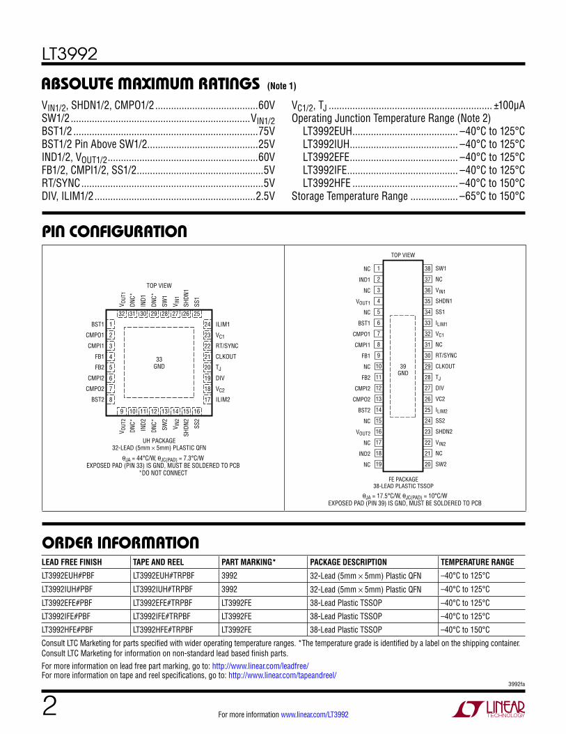
absoluTe MaxiMuM raTingsVIN1/2, SHDN1/2, CMPO1/2 .......................................60VSW1/2 ....................................................................VIN1/2BST1/2 ......................................................................75VBST1/2 Pin Above SW1/2 ..........................................25VIND1/2, VOUT1/2 .........................................................60VFB1/2, CMPI1/2, SS1/2 ................................................5VRT/SYNC .....................................................................5VDIV, ILIM1/2 .............................................................2.5V
(Note 1)
pin conFiguraTion
orDer inForMaTionLEAD FREE FINISH TAPE AND REEL PART MARKING* PACKAGE DESCRIPTION TEMPERATURE RANGE
LT3992EUH#PBF LT3992EUH#TRPBF 3992 32-Lead (5mm × 5mm) Plastic QFN –40°C to 125°C
LT3992IUH#PBF LT3992IUH#TRPBF 3992 32-Lead (5mm × 5mm) Plastic QFN –40°C to 125°C
LT3992EFE#PBF LT3992EFE#TRPBF LT3992FE 38-Lead Plastic TSSOP –40°C to 125°C
LT3992IFE#PBF LT3992IFE#TRPBF LT3992FE 38-Lead Plastic TSSOP –40°C to 125°C
LT3992HFE#PBF LT3992HFE#TRPBF LT3992FE 38-Lead Plastic TSSOP –40°C to 150°C
Consult LTC Marketing for parts specified with wider operating temperature ranges. *The temperature grade is identified by a label on the shipping container. Consult LTC Marketing for information on non-standard lead based finish parts.For more information on lead free part marking, go to: http://www.linear.com/leadfree/ For more information on tape and reel specifications, go to: http://www.linear.com/tapeandreel/
VC1/2, TJ .............................................................. ±100µAOperating Junction Temperature Range (Note 2) LT3992EUH ........................................ –40°C to 125°C LT3992IUH ......................................... –40°C to 125°C LT3992EFE ......................................... –40°C to 125°C LT3992IFE .......................................... –40°C to 125°C LT3992HFE ........................................ –40°C to 150°CStorage Temperature Range .................. –65°C to 150°C
32 31 30 29 28 27 26 25
9 10 11 12
TOP VIEW
33GND
UH PACKAGE32-LEAD (5mm × 5mm) PLASTIC QFN
13 14 15 16
17
18
19
20
21
22
23
24
8
7
6
5
4
3
2
1BST1
CMPO1
CMPI1
FB1
FB2
CMPI2
CMPO2
BST2
ILIM1
VC1
RT/SYNC
CLKOUT
TJ
DIV
VC2
ILIM2
V OUT
1
DNC*
IND1
DNC*
SW1
V IN1
SHDN
1
SS1
V OUT
2
DNC*
IND2
DNC*
SW2
V IN2
SHDN
2
SS2
θJA = 44°C/W, θJC(PAD) = 7.3°C/W
EXPOSED PAD (PIN 33) IS GND, MUST BE SOLDERED TO PCB*DO NOT CONNECT
1
2
3
4
5
6
7
8
9
10
11
12
13
14
15
16
17
18
19
TOP VIEW
FE PACKAGE38-LEAD PLASTIC TSSOP
38
37
36
35
34
33
32
31
30
29
28
27
26
25
24
23
22
21
20
NC
IND1
NC
VOUT1
NC
BST1
CMPO1
CMPI1
FB1
NC
FB2
CMPI2
CMPO2
BST2
NC
VOUT2
NC
IND2
NC
SW1
NC
VIN1
SHDN1
SS1
ILIM1
VC1
NC
RT/SYNC
CLKOUT
TJ
DIV
VC2
ILIM2
SS2
SHDN2
VIN2
NC
SW2
39GND
θJA = 17.5°C/W, θJC(PAD) = 10°C/W EXPOSED PAD (PIN 39) IS GND, MUST BE SOLDERED TO PCB
LT3992
33992fa
For more information www.linear.com/LT3992
elecTrical characTerisTics The l denotes the specifications which apply over the full operating temperature range, otherwise specifications are at TA = 25°C. VVIN1/2 = 15V unless otherwise specified. (Note 2)
PARAMETER CONDITIONS MIN TYP MAX UNITS
SHDN Voltage Threshold CH1/2 l 1.24 1.32 1.4 V
SHDN Input Current CH1/2 VSHDN = 1.35V –1 0 1 µA
VIN1 Undervoltage Lockout (Note 3) 2.6 2.9 3.2 V
VIN1 Shutdown Current VSHDN = 0V l 6 13 µA
VIN2 Shutdown Current VSHDN = 0V l 0.1 2 µA
VIN1 Quiescent Current VFB1/2 = 2V 3 4.2 6 mA
VIN2 Quiescent Current VFB1/2 = 2V 300 530 900 µA
Feedback Voltage CH1/2 VVC1/2 = 1V l 786 806 824 mV
Feedback Voltage Regulation VVIN1/2 = 4V to 60V l 780 806 830 mV
Feedback Voltage Offset CH1 to CH2 VVC1/2 = 1V l –13 0 13 mV
Feedback Bias Current CH1/2 VVC1/2 = 1V l 0 85 300 nA
TJ Output Voltage (Note 4) TJ = 25°C, ITJ = 25µA, Temperature = 25°C ITJ = 25µA, Temperature = 125°C ITJ = 25µA, Temperature = –40°C
250 1.23 –380
mV V
mV
TJ Error Temperature = 25°C to 125°C l –100 0 100 mV
Error Amp gm CH1/2 VVC1/2 = 1V, IVC1/2 = ±10µA 250 350 450 µMho
Error Amp Source Current CH1/2 VFB1/2 = 0.7V, VVC1/2 = 1V 15 25 40 µA
Error Amp Sink Current CH1/2 VFB1/2 =0.9V, VVC1/2 = 1V 15 25 40 µA
Error Amp High Clamp CH1/2 VFB1/2 = 0.7V 1.7 1.9 2.1 V
Error Amp Switching Threshold CH1/2 VFB1/2 = 0V 0.8 1.0 1.2 V
Soft-Start Source Current CH1/2 VFB1/2 = 2V, VSS1/2 = 0.07V l 9 13.5 17 µA
Soft-Start VOH CH1/2 VFB1/2 = 2.0V 1.9 2.15 2.4 V
Soft-Start Sink Current CH1/2 VFB1/2 = 0.7V, VSS1/2 = 2V 0.4 0.9 2 mA
Soft-Start VOL CH1/2 VFB1/2 = 0V 130 170 210 mV
Soft-Start to Feedback Offset CH1/2 VVC1/2 = 1V, VSS1/2 = 0.4V l 16 0 16 mV
SS POR Threshold CH1/2 70 110 140 mV
Soft-Start Sink Current CH1/2 POR VFB1/2 = 2V, VSS1/2 = 0.14V (Note 5) 150 450 600 µA
Soft-Start SW Disable CH1/2 VFB1/2 = 0V (Note 5) 80 115 150 mV
CMPI Bias Current CH1/2 VCMPI1/2 = 0.8V –100 0 100 nA
CMPO Leakage CH1/2 VCMP1/2 = 0.8V, VCMPO1/2 = 60V 70 500 nA
CMPI Threshold CH1/2 VCMPI1/2 Rising l 690 725 760 mV
CMPI Threshold CH1/2 of VFB1/2 VCMPI1/2 Rising (Note 6) 86 90 94 %
CMPI Hysteresis CH1/2 VCMPI1/2 50 80 105 mV
CMPO Sink Current CH1/2 VCMPI1/2 = 0.6V, VCMPO1/2 = 0.2V 150 250 µA
RT/SYNC Reference Current VRT/SYNC = 0.36V E- & I-Grade l 11.3 12 12.7 µA
RT/SYNC Reference Current VRT/SYNC = 0.36V H-Grade l 11.2 12 13 µA
Minimum Switching Frequency RRT/SYNC =0Ω 50 110 150 kHz
Switching Frequency RRT/SYNC = 28k 900 1000 1100 kHz
Maximum Switching Frequency RRT/SYNC =100k 2.2 2.5 3.0 MHz
Switching Phase Angle CH1 ≥ CH2 185 Deg
DIV Reference Current VDIV = 1V l 10.7 12 13.3 µA
CH1 DIV 2 Threshold RRT/SYNC = 0V 0.44 0.5 0.56 V

LT3992
43992fa
For more information www.linear.com/LT3992
elecTrical characTerisTics The l denotes the specifications which apply over the full operating temperature range, otherwise specifications are at TA = 25°C. VVIN1/2 = 15V unless otherwise specified. (Note 2)
PARAMETER CONDITIONS MIN TYP MAX UNITS
CH1 DIV 4 Threshold RRT/SYNC = 0V 0.89 1.0 1.06 V
CH1 DIV 8 Threshold RRT/SYNC = 0V 1.39 1.5 1.56 V
CLKOUT VOL 0.25 V
CLKOUT VOH 2 V
CLKOUT to SW1ON Delay ( tDCLKOSW1) CLKOUT Rising 60 ns
CLKOUT to SW2ON Delay ( tDCLKOSW2) CLKOUT Falling 30 ns
RT/SYNC to CLKOUT Delay ( tDRTSYNCH) VRT/SYNC = 0V to 2V Rising Edge 300 ns
RT/SYNC to CLKOUT Delay ( tDRTSYNCL) VRT/SYNC = 2V to 0V Falling Edge 150 ns
SYNC Frequency Range 250 2000 kHz
SYNC Phase Angle CH1 to CH2 SYNC Frequency = 250kHz 180 Deg
Minimum Switch On-Time CH1/2 160 ns
Minimum Switch Off-Time CH1/2 200 ns
Minimum Boost for 100% DC CH1/2 (Note 7) 1.6 2.2 2.6 V
IND + VOUT Current CH1/2 VVOUT1/2 = 0V VVOUT1/2 = 5V
1.5 0.5
5 5
µA µA
ILIM1/2 Reference Current VILIM = 0V l 10 12 16 µA
IND to VOUT Maximum Current CH1/2 VILIM1/2 = 0.5V, VVOUT = 1V (Note 8) VILIM1/2 = 0.5V, VVOUT = 5V (Note 8) VILIM1/2 = 1.5V, VVOUT = 1V (Note 8) VILIM1/2 = 1.5V, VVOUT = 5V (Note 8)
l
l
0.5 0.7 3.5 3.5
1.5 1.8 4.6 4.6
3 3
6.4 6.4
A A A A
Switch Leakage Current CH1/2 VSW1/2 = 0V l 1 10 µA
Switch Saturation Voltage CH1/2 ISW1/2 = 500mA, VBST1/2 = 18V ISW1/2 = 3A, VBST1/2 = 18V
200 325
mV mV
Boost Current CH1/2 ISW1/2 = 500mA, VBST1/2 = 8V ISW1/2 = 3A, VBST1/2 = 8V
5 35
8 55
25 85
mA mA
Minimum Boost Voltage CH1/2 (Note 9) ISW1/2 = 3A, VBST1/2 = 8V 1.0 2.2 3.0 V
Note 1: Stresses beyond those listed under Absolute Maximum Ratings may cause permanent damage to the device. Exposure to any Absolute Maximum Rating condition for extended periods may affect device reliability and lifetime.Note 2: The LT3992EUH/LT3992EFE is guaranteed to meet performance specifications from 0°C to 125°C junction temperature. Specifications over the –40°C to 125°C operating junction temperature range are assured by design, characterization and correlation with statistical process controls. The LT3992IUH/LT3992IFE is guaranteed over the full –40°C to 125°C operating junction temperature range. The LT3992HFE is guaranteed over the full –40°C to 150°C operating junction temperature range. High junction temperatures degrade operating lifetimes. Operating lifetime is derated at junction temperatures greater than 125°C.Note 3: VIN undervoltage lockout is defined as the voltage which the VIN pin must exceed for operation. The threshold guarantees that internal bias lines are regulated and switching frequency is constant. Actual minimum input voltage to maintain a regulated output will depend upon output voltage and load current. See the Applications Information section.
Note 4: The TJ output voltage represents the temperature at the center of the die while dissipating quiescent power. Due to switch power dissipation and temperature gradients across the die, the TJ output voltage measurement does not guarantee that absolute maximum junction temperature will not be exceeded.Note 5: An internal power on reset (POR) latch is set on the positive transition of the SHDN1/2 pin through its threshold, thermal shutdown or overvoltage lockout. The output of the latch activates current sources on each SS pin which typically sink 450µA and discharge the SS capacitor. The latch is reset when both SS pins are driven below the soft-start POR threshold or the SHDN pin is taken below its threshold.Note 6: The threshold is expressed as a percentage of the feedback reference voltage for the channel.Note 7: To enhance dropout operation, the output switch will be turned off for the minimum off-time only when the voltage across the boost capacitor drops below the minimum boost for 100% duty cycle threshold.Note 8: The IND to VOUT maximum current is defined as the value of current flowing from the IND pin to the VOUT pin which resets the switch latch when the VC pin is at its high clamp. Note 9: This is the minimum voltage across the boost capacitor needed to guarantee full saturation of the internal power switch.
LT3992
53992fa
For more information www.linear.com/LT3992
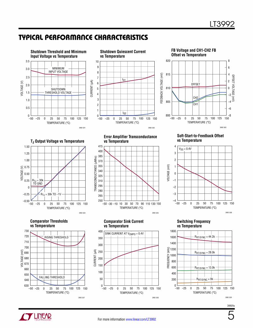
Typical perForMance characTerisTics
Shutdown Threshold and Minimum Input Voltage vs Temperature
Shutdown Quiescent Current vs Temperature
FB Voltage and CH1-CH2 FB Offset vs Temperature
TJ Output Voltage vs TemperatureError Amplifier Transconductance vs Temperature
Soft-Start-to-Feedback Offset vs Temperature
Comparator Thresholds vs Temperature
TEMPERATURE (°C)–50
VOLT
AGE
(V)
2.0
2.5
3.0
25 50 75 100 125
3992 G01
1.5
1.0
–25 0 150
0.5
0
3.5
MINIMUMINPUT VOLTAGE
SHUTDOWNTHRESHOLD VOLTAGE
TEMPERATURE (°C)–50
0
CURR
ENT
(µA)
2
1
3
5
4
7
6
0 50 100 150
3992 G02
9
8
10
IQ1
IQ2
–25 25 75 125TEMPERATURE (°C)
–50800
FEED
BACK
VOL
TAGE
(mV) OFFSET VOLTAGE (m
V)
820
815
810
805
0 50 75
3992 G03
–8
–4
–6
8
4
0
–2
6
2
–25 25 100
CH1
CH2
125 150
OFFSET
TEMPERATURE (°C)–50
VOLT
AGE
(V)
0.50
1.00
150
3992 G04
0
–0.500 50 100–25 25 75 125
1.50
0.25
0.75
–0.25
1.25
RTJ = 30kTO GND
RTJ = 30k TO –1V
TEMPERATURE (°C)–50
TRAN
SCON
DUCT
ANCE
(µM
ho)
295
385
400
415
10 50 70 90
3992 G05
265
355
325
280
370
250
340
310
–30 –10 30 130110 150TEMPERATURE (°C)
–50
VOLT
AGE
(mV)
0
2
150
3992 G06
–2
–40 50 100–25 25 75 125
4
–1
1
–3
3VSS = 0.4V
TEMPERATURE (°C)–50
630
VOLT
AGE
(mV)
640
660
670
680
730
700
0 50 75
3992 G07
650
710
720
690
–25 25 100 125 150
RISING THRESHOLD
FALLING THRESHOLD
Comparator Sink Current vs Temperature
Switching Frequency vs Temperature
TEMPERATURE (°C)–50
CURR
ENT
(µA)
200
300
150
3992 G08
100
00 50 100–25 25 75 125
400
150
250
50
350
SINK CURRENT AT VCMPO = 0.4V
TEMPERATURE (°C)–50
FREQ
UENC
Y (k
Hz)
1000
1200
1400
150
3992 G09
800
400
600
00 50 100–25 25 75 125
200
1800
1600 RRT/SYNC = 44.2k
RRT/SYNC = 28.0k
RRT/SYNC = 13.0k
RRT/SYNC = 0k

LT3992
63992fa
For more information www.linear.com/LT3992
Typical perForMance characTerisTics
Switching Phase vs TemperatureCLKOUT-to-SW1 Delay vs Temperature
RT/SYNC-to-CLKOUT and SW1 Delay vs Temperature
Synchronization Duty Cycles vs Temperature
DIV Voltage Threshold vs Temperature
Switch Saturation Voltage vs Temperature
Boost Current vs TemperatureMinimum Boost Voltage vs Temperature
Switch Peak Current vs Temperature
TEMPERATURE (°C)–50
PHAS
E (D
EG)
187
191
150
3992 G10
183
181
179
1750 50 100–25 25 75 125
195
185
189
177
193
TEMPERATURE (°C)–50
60
DELA
Y (n
s)
70
90
100
110
160
130
0 50 75
3992 G11
80
140
150
120
–25 25 100 125 150TEMPERATURE (°C)
–50
DELA
Y (n
s)
250
300
350
150
3992 G12
200
150
00 50 100–25 25 75 125
100
50
450
400SW1
CLKOUT
TEMPERATURE (°C)–50
0
DUTY
CYC
LE (%
)
10
30
40
50
100
70
0 50 75
3992 G13
20
80
90
60
–25 25 100 125 150
RT/SYNC FREQUENCY = 1MHz
MAXIMUM RT/SYNC DUTY CYCLE
MINIMUM RT/SYNC DUTY CYCLE
TEMPERATURE (°C)–50
VOLT
AGE
(V)
1.0
1.2
1.4
150
3992 G14
0.8
0.6
00 50 100–25 25 75 125
0.4
0.2
1.8
1.6 ÷8
÷4
÷2
TEMPERATURE (°C)–50
100
VOLT
AGE
(mV)
150
200
250
300
0 50 100 150
3992 G15
350
400
–25 25 75 125
ISW = 3A
ISW = 1A
ISW = 500mA
TEMPERATURE (°C)–50
0
BOOS
T CU
RREN
T (m
A)
10
30
40
50
100
70
0 50 75
3992 G16
20
80
90
60
–25 25 100 125 150
0.5A
1A
3A
TEMPERATURE (°C)–50
0
PEAK
CUR
RENT
(A)
0.5
1.5
2.0
2.5
5.0
3.5
0 50 75
3992 G17
1.0
4.0
4.5
3.0
–25 25 100 125 150
VILIM = 1.5V
VILIM = 0.5V
TEMPERATURE (°C)–50
VOLT
AGE
(V)
2.00
2.50
150
3992 G18
1.50
1.000 50 100–25 25 75 125
3.00
1.75
2.25
1.25
2.75
ISW = 3A
LT3992
73992fa
For more information www.linear.com/LT3992
Typical perForMance characTerisTics
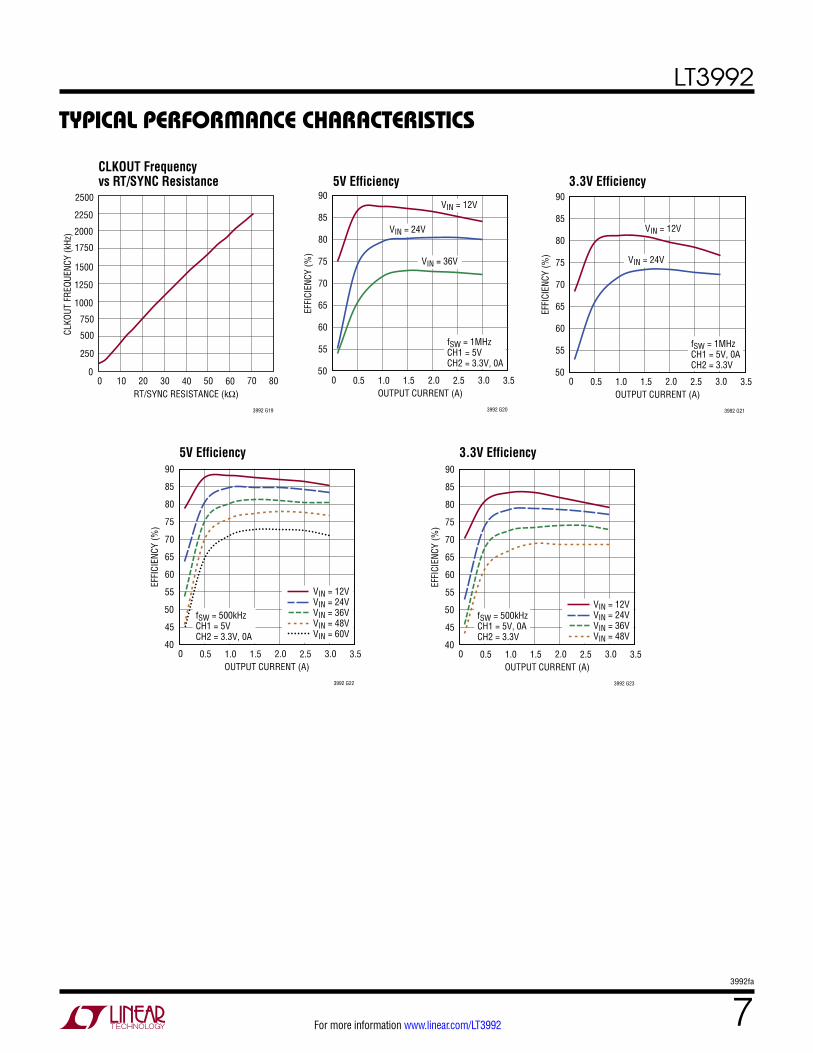
CLKOUT Frequency vs RT/SYNC Resistance 5V Efficiency 3.3V Efficiency
RT/SYNC RESISTANCE (kΩ)0
0
CLKO
UT F
REQU
ENCY
(kHz
)
250
500
750
1500
1750
2000
2250
2500
20 40 50 80
3992 G19
1000
1250
10 30 60 70OUTPUT CURRENT (A)
050
EFFI
CIEN
CY (%
)
70
75
80
90
1.0 2.0 2.5
3992 G20
65
60
55
85
0.5 1.5 3.0 3.5
VIN = 12V
VIN = 24V
VIN = 36V
fSW = 1MHzCH1 = 5VCH2 = 3.3V, 0A
OUTPUT CURRENT (A)0
50
EFFI
CIEN
CY (%
)
70
75
80
90
1.0 2.0 2.5
3992 G21
65
60
55
85
0.5 1.5 3.0 3.5
VIN = 12V
VIN = 24V
fSW = 1MHzCH1 = 5V, 0ACH2 = 3.3V
5V Efficiency 3.3V Efficiency
OUTPUT CURRENT (A)0
40
EFFI
CIEN
CY (%
)
70
75
80
90
1.0 2.0 2.5
3992 G22
65
60
45
50
55
85
0.5 1.5 3.0 3.5
fSW = 500kHzCH1 = 5VCH2 = 3.3V, 0A
VIN = 12VVIN = 24VVIN = 36VVIN = 48VVIN = 60V
OUTPUT CURRENT (A)0
40
EFFI
CIEN
CY (%
)
70
75
80
90
1.0 2.0 2.5
3992 G23
65
60
45
50
55
85
0.5 1.5 3.0 3.5
fSW = 500kHzCH1 = 5V, 0ACH2 = 3.3V
VIN = 12VVIN = 24VVIN = 36VVIN = 48V

LT3992
83992fa
For more information www.linear.com/LT3992
pin FuncTionsBST1/2: The BST pin provides a higher than VIN base drive to the power NPN to ensure a low switch drop. If the voltage between the BST pin and the VIN pin is less than the voltage required to fully turn on the power NPN, the power switch is turned off to recharge the BST capacitor.
CMPI1/2: The CMPI pin is an input to a comparator with a threshold of 725mV and 80mV of hysteresis. Connecting the CMPI pin to the FB pin will generate a power good signal when the output is within 90% of its regulated value.
CMPO1/2: The CMPO pin is an open-collector output that sinks current when the CMPI pin falls below its threshold. For a typical input voltage above 2.9V, its output state re-mains true, although during shutdown, VIN1 undervoltage lockout or thermal shutdown, its current sink capability is reduced. The COMPO pins can be left open circuit or tied together to form a single power good signal.
DIV: The voltage present at the DIV pin determines the ratio of channel 1 frequency to the master clock frequency set by the RT/SYNC pin. The DIV pin is driven by an internal current source with a typical value of 12µA which allows a single resistor from the DIV pin to ground to set the DIV voltage and resulting channel 1 frequency divider. Ratios of 1, 2, 4 and 8 are available. See the Applications Information section for more information.
DNC: Do Not Connect.
GND: The exposed pad pin is the only ground connec-tion for the device. The exposed pad should be soldered to a large copper area to reduce thermal resistance. The GND pin is common to both channels and also serves as small-signal ground. For ideal operation all small-signal ground paths should connect to the GND pin at a single point avoiding any high current ground returns.
FB1/2: The FB pin is the negative input to the error amplifier. The output switches to regulate this pin to 806mV with respect to the exposed ground pad. Bias current flows out of the FB pin.
ILIM1/2: The voltage present at the ILIM pin determines the peak inductor current for the channel. The ILIM pin is driven by an internal current source with a typical value of 12µA. A resistor from the ILIM pin to ground sets the ILIM voltage; the resistor value must be between 42.2k and 120k. The maximum current limit range is 4.8A to 1.8A when the ILIM voltages are 1V and 0.5V respectively.
IND1/2: The IND pin is the input to the internal sense resistor that measures current flowing in the inductor. When the current in the resistor exceeds the current dictated by the VC pin, the SW latch is held in reset, disabling the output switch. Bias current flows out of the IND pin.
RT/SYNC: The voltage present at the RT/SYNC pin deter-mines the constant switching frequency. The RT/SYNC pin is driven by an internal current source with a typical value of 12µA which allows a single resistor from the RT/SYNC pin to ground to set the RT/SYNC voltage and result-ing switching frequency. Minimum switching frequency is typically 110kHz when VRT/SYNC is 0V and maximum switching frequency is typically 2.5MHz when VRT/SYNC is above 950mV.
Driving the RT/SYNC pin with an external clock signal will synchronize the switch to the applied frequency. Synchro-nization occurs on the rising edge of the clock signal after the clock signal is detected. Each rising clock edge initiates an oscillator ramp reset. A gain control loop servos the oscillator charging current to maintain constant oscillator amplitude. Hence, the slope compensation and channel phase relationship remain unchanged. If the clock signal is removed, the oscillator reverts to resistor mode after the synchronization detection circuitry times out. The clock source impedance should be set such that the current out of the RT/SYNC pin in resistor mode generates a frequency roughly equivalent to the synchronization frequency. See the Applications Information section for more information.
LT3992
93992fa
For more information www.linear.com/LT3992
pin FuncTionsSHDN1/2: The shutdown pin is used to control each channel’s operation. In addition to controlling channel 1, the SHDN1 pin also activates control circuitry for both channels and must be present for channel 2 to operate. When SHDN1 is below its threshold, quiescent current is reduced to a typical value of 6µA. Independent channel UVLO can be programmed by connecting the SHDN pin to an input voltage divider. See the Applications Information section for more information. If the shutdown features are not used, the SHDN pin should be tied to VIN.
SS1/2: Current flowing out the SS pin into an external capacitor defines the rise time of the output voltage. When the SS pin is lower than the 0.806V reference, the feedback is regulated to the SS voltage. When the SS pin exceeds the reference voltage, the output will regulate the FB pin voltage to 0.806V and the SS pin will continue to rise until its clamp voltage. During an output overload, the VC pin is driven above the maximum switch current level activating its voltage clamp. When the VC clamp is activated, the SS pin is discharged until the output reaches a regulation point that the maximum output current can maintain. When the overload condition is removed, the output soft starts from that voltage. In the case of a SHDN or thermal shutdown event, a power on reset latch ensures the capacitors on both channels are fully discharged before either is released. Connecting both SS pins together ensures the outputs track together.
CLKOUT: The CLKOUT pin generates a square wave of 0V to 2.5V which is synchronized to the internal oscillator. If the switching frequency is set by an external resistor the resultant clock duty cycle will be 50%. If the RT/SYNC pin is driven by an external clock source, the resultant CLKOUT duty cycle will mirror the external source.
SW1/2: The SW pin is the emitter of the internal power NPN. At switch off, the inductor will drive this pin below ground with a high dV/dt. An external Schottky catch diode to ground, close to the SW pin and respective VIN decoupling capacitor’s ground, must be used to prevent this pin from excessive negative voltages.
TJ: The TJ pin outputs a voltage proportional to junction temperature. The pin is 250mV for 25°C and has a slope of 10mV/°C. See the Applications Information section for more information.
VC1/2: The VC pin is the output of the error amplifier and the input to the peak switch current comparator. It is normally used for frequency compensation, but can also be used as a current clamp or control loop override. If the error amplifier drives VC above the maximum switch current level, a voltage clamp activates. This indicates that the output is overloaded and current is pulled from the SS pin reducing the regulation point.
VIN1: The VIN1 pin powers the internal control circuitry for both channels and is monitored by an undervoltage lockout comparator. The VIN1 pin is also connected to the collector of channel 1’s on-chip power NPN switch. The VIN1 pin has high dI/dt edges and must be decoupled to ground close to the pin of the device.
VIN2: The VIN2 pin powers the output stage for channel 2 and is monitored by an undervoltage lockout comparator. VIN1 voltage must be greater than typically 2.9V for VIN2 operation. The VIN2 pin is also the collector of channel 2’s on-chip power NPN switch. The VIN2 pin has high dI/dt edges and must be decoupled to ground close to the pin of the device.
VOUT1/2: The VOUT pin is the output to the internal sense resistor that measures current flowing in the inductor. When the current in the resistor exceeds the current dic-tated by the VC pin, the SW latch is held in reset disabling the output switch. Bias current flows out of the VOUT pin.
LT3992
103992fa
For more information www.linear.com/LT3992
block DiagraM
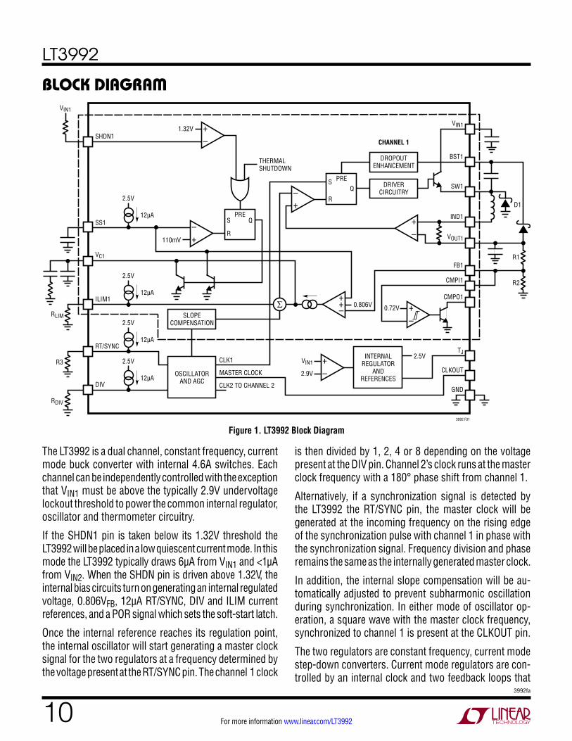
Figure 1. LT3992 Block Diagram
The LT3992 is a dual channel, constant frequency, current mode buck converter with internal 4.6A switches. Each channel can be independently controlled with the exception that VIN1 must be above the typically 2.9V undervoltage lockout threshold to power the common internal regulator, oscillator and thermometer circuitry.
If the SHDN1 pin is taken below its 1.32V threshold the LT3992 will be placed in a low quiescent current mode. In this mode the LT3992 typically draws 6µA from VIN1 and <1µA from VIN2. When the SHDN pin is driven above 1.32V, the internal bias circuits turn on generating an internal regulated voltage, 0.806VFB, 12µA RT/SYNC, DIV and ILIM current references, and a POR signal which sets the soft-start latch.
Once the internal reference reaches its regulation point, the internal oscillator will start generating a master clock signal for the two regulators at a frequency determined by the voltage present at the RT/SYNC pin. The channel 1 clock
is then divided by 1, 2, 4 or 8 depending on the voltage present at the DIV pin. Channel 2’s clock runs at the master clock frequency with a 180° phase shift from channel 1.
Alternatively, if a synchronization signal is detected by the LT3992 the RT/SYNC pin, the master clock will be generated at the incoming frequency on the rising edge of the synchronization pulse with channel 1 in phase with the synchronization signal. Frequency division and phase remains the same as the internally generated master clock.
In addition, the internal slope compensation will be au-tomatically adjusted to prevent subharmonic oscillation during synchronization. In either mode of oscillator op-eration, a square wave with the master clock frequency, synchronized to channel 1 is present at the CLKOUT pin.
The two regulators are constant frequency, current mode step-down converters. Current mode regulators are con-trolled by an internal clock and two feedback loops that
2.9V
3992 F01
+–
VIN1
+–
+–
++–
1.32V
THERMALSHUTDOWN
VIN1
SHDN1
SS1
VC1
110mV+–
12µA
2.5V
12µA
2.5V
ILIM1
RLIM
PRE
SLOPECOMPENSATION
DRIVERCIRCUITRY
DROPOUTENHANCEMENT
CHANNEL 1
OSCILLATORAND AGC
INTERNALREGULATOR
ANDREFERENCES
CLK2 TO CHANNEL 2
MASTER CLOCK
CLK1
0.806V
2.5V
0.72V
S Q
R
+–
PRESQ
R
12µA
2.5V
RT/SYNC
12µA
2.5V
DIV
R3
RDIV
BST1
SW1
IND1
FB1R1
D1
R2CMPI1
CMPO1
TJ
CLKOUT
GND
VOUT1
VIN1
+–

LT3992
113992fa
For more information www.linear.com/LT3992
block DiagraMcontrol the duty cycle of the power switch. In addition to the normal error amplifier, there is a current sense amplifier that monitors switch current on a cycle-by-cycle basis. This technique means that the error amplifier commands current to be delivered to the output rather than voltage. A voltage fed system will have low phase shift up to the resonant frequency of the inductor and output capacitor, then an abrupt 180° shift will occur. The current fed sys-tem will have 90° phase shift at a much lower frequency, but will not have the additional 90° shift until well beyond the LC resonant frequency. This makes it much easier to frequency compensate the feedback loop and also gives much quicker transient response.
The Block Diagram in Figure 1 shows only one of the switching regulators whose operation will be discussed below. The additional regulator will operate in a similar manner with the exception that its clock will be 180° out of phase with the other regulator.
When, during power-up, an internal POR signal sets the soft-start latch, both SS pins will be discharged to ground to ensure proper start-up operation. When the SS pin voltage drops below 110mV, the VC pin is driven low disabling switching and the soft-start latch is reset. Once the latch is reset the soft-start capacitor starts to charge with a typical value of 12µA.
As the voltage rises above 110mV on the SS pin, the VC pin will be driven high by the error amplifier. When the voltage on the VC pin exceeds 1V, the clock set-pulse sets the driver flip-flop, which turns on the internal power NPN switch. This causes current from VIN, through the NPN switch, inductor and internal sense resistor to increase. When the voltage drop across the internal sense resistor exceeds a predetermined level set by the voltage on the VC pin, the flip-flop is reset and the internal NPN switch is turned off. Once the switch is turned off the inductor will drive the voltage at the SW pin low until the external Schottky diode starts to conduct, decreasing the current in the inductor. The cycle is repeated with the start of each clock cycle. However, if the internal sense resistor voltage exceeds the predetermined level at the start of a clock cycle, the flip-flop will not be set resulting in a further decrease in inductor current. Since the output current is controlled
by the VC voltage, output regulation is achieved by the error amplifier continually adjusting the VC pin voltage.
The error amplifier is a transconductance amplifier that compares the FB voltage to the lowest voltage present at either the SS pin or an internal 806mV reference. Compen-sation of the loop is easily achieved with a simple capacitor or series resistor/capacitor from the VC pin to ground.
The regulators’ maximum output current occurs when the VC pin is driven to its maximum clamp value by the error amplifier. The value of the typical maximum switch current can be programmed from 4.6A to 1.8A by placing a resistor from the ILIM pin to ground.
Since the SS pin is driven by a constant current source, a single capacitor on the soft-start pin will generate controlled linear ramp on the output voltage.
If the current demanded by the output exceeds the maxi-mum current dictated by the VC pin clamp, the SS pin will be discharged, lowering the regulation point until the output voltage can be supported by the maximum current. Once the overload condition is removed, the regulator will soft-start from the overload regulation point.
Shutdown control or thermal shutdown will set the soft-start latch, resulting in a complete soft-start sequence.
The switch driver operates from either the VIN or BST volt-age. An external diode and capacitor are used to generate a drive voltage higher than VIN to saturate the output NPN and maintain high efficiency. If the BST capacitor voltage is sufficient, the switch is allowed to operate to 100% duty cycle. If the boost capacitor discharges towards a level insufficient to drive the output NPN, a BST pin compara-tor forces a minimum cycle off time, allowing the boost capacitor to recharge.
A comparator with a threshold of 720mV and 80mV of hysteresis is provided for detecting error conditions. The CMPO output is an open-collector NPN that is off when the CMPI pin is above the threshold allowing a resistor to pull the CMPO pin to a desired voltage.
The voltage present at the TJ pin is proportional to the junction temperature of the LT3992. The TJ pin will be 250mV for a die temperature of 25°C and will have a slope of 10mV/°C.

LT3992
123992fa
For more information www.linear.com/LT3992
applicaTions inForMaTionChoosing the Output Voltage
The output voltage is programmed with a resistor divider between the output and the FB pin. Choose the 1% resis-tors according to:
R1=R2 •
VOUT0.806
–1⎛⎝⎜
⎞⎠⎟
R2 should be 10k or less to avoid bias current errors. Ref-erence designators refer to the Block Diagram in Figure 1.
Choosing the Switching Frequency
The LT3992 switching frequency is set by resistor R3 in Figure 1. The RT/SYNC pin is driven by a 12µA current source. Setting resistor R3 sets the voltage present at the RT/SYNC pin which determines the master oscillator frequency as illustrated in Figure 2. The R3 resistance (in kΩ) may be calculated from the desired switching frequency (in kHz) by the equation:
R3 = 1.86E-6 • fSW2 + 2.81E-2 • fSW –1.76
for frequencies between 150kHz and 2000kHz. A 0V to 2.5V square wave with the same frequency as the master oscillator and in phase with channel 1 is output via the CLKOUT pin. The CLKOUT signal can be used to synchro-nize multiple switching regulators.
Figure 2. Switching Frequency vs RT/SYNC Resistance
RT/SYNC RESISTANCE (kΩ)0
0
CLKO
UT F
REQU
ENCY
(kHz
)
250
500
750
1500
1750
2000
2250
2500
20 40 50 80
3992 F02
1000
1250
10 30 60 70
To alleviate duty cycle restrictions due to minimum switch-on times, channel 1’s switching frequency can be divided from the master clock by 1, 2, 4 or 8 determined by resistor RDIV in Figure 1. Channel 2’s switching frequency is not affected by the DIV pin. The DIV pin is driven by a 12µA current source. Setting resistor RDIV sets the voltage pres-ent at the DIV pin which determines the divisor as shown in Table 1. The DIV pin doesn’t have any input hysteresis near the ratio thresholds.
Table 1. Channel 1 Divisor vs VDIV
TYPICAL DIV VOLTAGE FREQUENCY RATIO RDIV (Ω)
VDIV < 0.5V 1 0
0.5V < VDIV < 1.0V 2 61.9k
1.0V < VDIV < 1.5V 4 102k
1.5V < VDIV 8 150k
The switching frequency is typically set as high as pos-sible to reduce overall solution size. The LT3992 employs techniques to enhance dropout at high frequencies but efficiency and maximum input voltage decrease due to switching losses and minimum switch on times.
The maximum recommended frequency can be approxi-mated by the equation:
Frequency(Hz)= VOUT +VD
VIN – VSW +VD•
1tON(MIN)
where VD is the forward voltage drop of the catch diode (D1 Figure 1), VSW is the voltage drop of the internal switch, and tON(MIN) in the minimum on-time of the switch.
LT3992
133992fa
For more information www.linear.com/LT3992
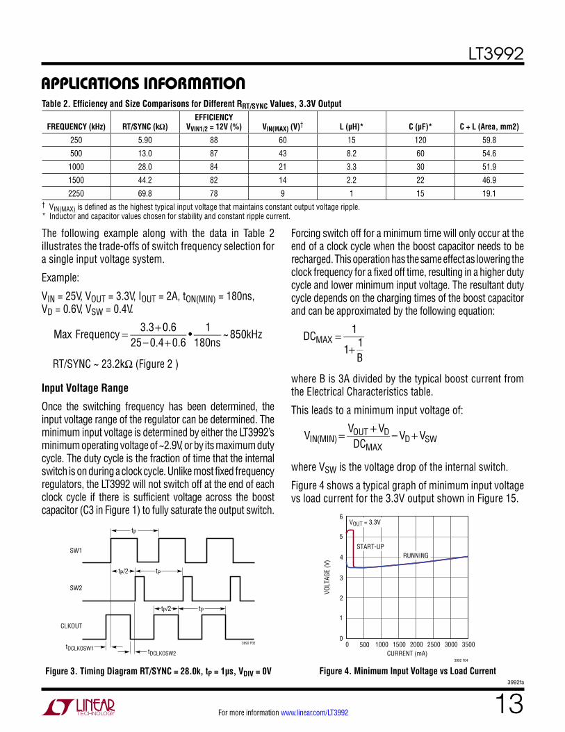
applicaTions inForMaTion
The following example along with the data in Table 2 illustrates the trade-offs of switch frequency selection for a single input voltage system.
Example:
VIN = 25V, VOUT = 3.3V, IOUT = 2A, tON(MIN) = 180ns, VD = 0.6V, VSW = 0.4V.
MaxFrequency = 3.3+0.6
25– 0.4+0.6•
1180ns
~850kHz
RT/SYNC ~ 23.2kΩ (Figure 2 )
Input Voltage Range
Once the switching frequency has been determined, the input voltage range of the regulator can be determined. The minimum input voltage is determined by either the LT3992’s minimum operating voltage of ~2.9V, or by its maximum duty cycle. The duty cycle is the fraction of time that the internal switch is on during a clock cycle. Unlike most fixed frequency regulators, the LT3992 will not switch off at the end of each clock cycle if there is sufficient voltage across the boost capacitor (C3 in Figure 1) to fully saturate the output switch.
Forcing switch off for a minimum time will only occur at the end of a clock cycle when the boost capacitor needs to be recharged. This operation has the same effect as lowering the clock frequency for a fixed off time, resulting in a higher duty cycle and lower minimum input voltage. The resultant duty cycle depends on the charging times of the boost capacitor and can be approximated by the following equation:
DCMAX = 1
1+ 1B
where B is 3A divided by the typical boost current from the Electrical Characteristics table.
This leads to a minimum input voltage of:
VIN(MIN)=
VOUT +VDDCMAX
– VD+VSW
where VSW is the voltage drop of the internal switch.
Figure 4 shows a typical graph of minimum input voltage vs load current for the 3.3V output shown in Figure 15.
Table 2. Efficiency and Size Comparisons for Different RRT/SYNC Values, 3.3V Output
FREQUENCY (kHz) RT/SYNC (kΩ)EFFICIENCY
VVIN1/2 = 12V (%) VIN(MAX) (V)† L (µH)* C (µF)* C + L (Area, mm2)
250 5.90 88 60 15 120 59.8
500 13.0 87 43 8.2 60 54.6
1000 28.0 84 21 3.3 30 51.9
1500 44.2 82 14 2.2 22 46.9
2250 69.8 78 9 1 15 19.1† VIN(MAX) is defined as the highest typical input voltage that maintains constant output voltage ripple. * Inductor and capacitor values chosen for stability and constant ripple current.
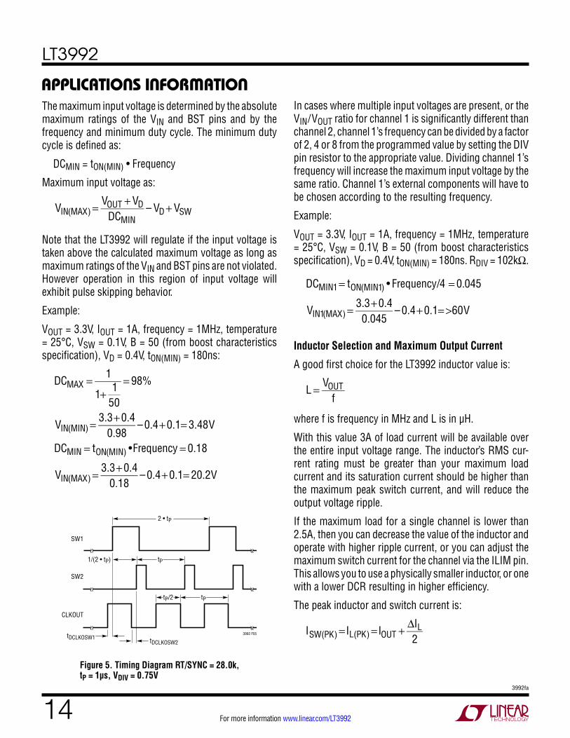
Figure 3. Timing Diagram RT/SYNC = 28.0k, tP = 1µs, VDIV = 0V Figure 4. Minimum Input Voltage vs Load Current
tP
tP
tP
tP/2
tP/2
tDCLKOSW2tDCLKOSW1
SW1
SW2
CLKOUT
3992 F03
CURRENT (mA)0
0
VOLT
AGE
(V)
1
2
3
4
6
500 1000 1500 2000
3992 F04
2500 35003000
5
VOUT = 3.3V
START-UPRUNNING
LT3992
143992fa
For more information www.linear.com/LT3992
applicaTions inForMaTionThe maximum input voltage is determined by the absolute maximum ratings of the VIN and BST pins and by the frequency and minimum duty cycle. The minimum duty cycle is defined as:
DCMIN = tON(MIN) • Frequency
Maximum input voltage as:
VIN(MAX)=
VOUT +VDDCMIN
– VD+VSW
Note that the LT3992 will regulate if the input voltage is taken above the calculated maximum voltage as long as maximum ratings of the VIN and BST pins are not violated. However operation in this region of input voltage will exhibit pulse skipping behavior.
Example:
VOUT = 3.3V, IOUT = 1A, frequency = 1MHz, temperature = 25°C, VSW = 0.1V, B = 50 (from boost characteristics specification), VD = 0.4V, tON(MIN) = 180ns:
DCMAX = 1
1+ 150
= 98%
VIN(MIN)=3.3+0.4
0.98– 0.4+0.1= 3.48V
DCMIN = tON(MIN) •Frequency = 0.18
VIN(MAX)=3.3+0.4
0.18– 0.4+0.1= 20.2V
In cases where multiple input voltages are present, or the VIN/VOUT ratio for channel 1 is significantly different than channel 2, channel 1’s frequency can be divided by a factor of 2, 4 or 8 from the programmed value by setting the DIV pin resistor to the appropriate value. Dividing channel 1’s frequency will increase the maximum input voltage by the same ratio. Channel 1’s external components will have to be chosen according to the resulting frequency.
Example:
VOUT = 3.3V, IOUT = 1A, frequency = 1MHz, temperature = 25°C, VSW = 0.1V, B = 50 (from boost characteristics specification), VD = 0.4V, tON(MIN) = 180ns. RDIV = 102kΩ.
DCMIN1= tON(MIN1) • Frequency/4 = 0.045
VIN1(MAX)=3.3+0.4
0.045– 0.4+0.1=>60V
Inductor Selection and Maximum Output Current
A good first choice for the LT3992 inductor value is:
L = VOUT
f
where f is frequency in MHz and L is in µH.
With this value 3A of load current will be available over the entire input voltage range. The inductor’s RMS cur-rent rating must be greater than your maximum load current and its saturation current should be higher than the maximum peak switch current, and will reduce the output voltage ripple.
If the maximum load for a single channel is lower than 2.5A, then you can decrease the value of the inductor and operate with higher ripple current, or you can adjust the maximum switch current for the channel via the ILIM pin. This allows you to use a physically smaller inductor, or one with a lower DCR resulting in higher efficiency.
The peak inductor and switch current is:
ISW(PK)= IL(PK)= IOUT +
ΔIL2
Figure 5. Timing Diagram RT/SYNC = 28.0k, tP = 1µs, VDIV = 0.75V
2 • tP
tP
tP
1/(2 • tP)
tP/2
tDCLKOSW2tDCLKOSW1
SW1
SW2
CLKOUT
3992 F05

LT3992
153992fa
For more information www.linear.com/LT3992
applicaTions inForMaTionTo maintain output regulation, this peak current must be less than the LT3992’s switch current limit, ILIM. ILIM can be set between 1.8A and 4.6A for each channel via a resistor from the ILIM pin to ground. The ILIM pin is driven by a 12µA current source. Setting resistor RLIM sets the voltage present at the ILIM pin which determines the maximum switch current as illustrated in Figure 6. The value for RLIM must be greater than 42.2k. A capacitor from the ILIM pin to ground, or a resistor divider from the output, can be used to limit the peak current during start-up. If a capacitor is used it must be discharged before power-up to ensure proper operation.
Referring to Figure 6, as the peak current limit is reduced, slope compensation further reduces the peak current with increasing duty cycle.
When the ILIM pin is used to reduce the peak switch cur-rent, the equation for inductor choice becomes:
L = 50 • VOUT
f •RILIM
where f is frequency in MHz, L in µH and R in kΩ.
When the LT3992’s input supplies are operated at different input voltages, an input capacitor sized for that channel should be placed as close as possible to the respective VIN pins.
A caution regarding the use of ceramic capacitors at the input. A ceramic input capacitor can combine with stray inductance to form a resonant tank circuit. If power is applied quickly (for example by plugging the circuit into a live power source) this tank can ring, doubling the in-put voltage and damaging the LT3992. The solution is to either clamp the input voltage or dampen the tank circuit by adding a lossy capacitor in parallel with the ceramic capacitor. For details, see Application Note 88.
Output Capacitor Selection
Typically step-down regulators are easily compensated with an output crossover frequency that is 1/10 of the switch-ing frequency. This means that the time that the output capacitor must supply the output load during a transient step is ~2 or 3 switching periods. With an allowable 1% drop in output voltage during the step, a good starting value for the output capacitor can be expressed by:
CVOUT =
MaxLoadStepFrequency •0.01• VOUT
Example:
VOUT = 3.3V, Frequency = 1MHz, Max Load Step = 2A.
CVOUT =
21E6•0.01•3.3V
= 60µF
The calculated value is only a suggested starting value. Increase the value if transient response needs improvement or reduce the capacitance if size is a priority. The output capacitor filters the inductor current to generate an output with low voltage ripple. It also stores energy in order to satisfy transient loads and to stabilize the LT3992’s control loop. The switching frequency of the LT3992 determines the value of output capacitance required. Also, the current mode control loop doesn’t require the presence of output capacitor series resistance (ESR). For these reasons, you are free to use ceramic capacitors to achieve very low output ripple and small circuit size.
Figure 6. Peak Switch Current vs ILIM Resistor
ILIM PIN RESISTOR (kΩ)40
1.0
PEAK
SW
ITCH
CUR
RENT
(A)
1.5
2.5
3.0
3.5
4.5
50 70
3992 F06
2.0
4.0
90 10060 80
Input Capacitor Selection
Bypass the inputs of the LT3992 circuit with a 4.7µF or higher ceramic capacitor of X7R or X5R type. A lower value or a less expensive Y5V type can be used if there is additional bypassing provided by bulk electrolytic or tantalum capacitors.
LT3992
163992fa
For more information www.linear.com/LT3992
applicaTions inForMaTionYou can also use electrolytic capacitors. The ESRs of most aluminum electrolytics are too large to deliver low output ripple. Tantalum and newer, lower ESR organic electrolytic capacitors intended for power supply use, are suitable and the manufacturers will specify the ESR. The choice of capacitor value will be based on the ESR required for low ripple. Because the volume of the capacitor determines its ESR, both the size and the value will be larger than a ceramic capacitor that would give you similar ripple per-formance. One benefit is that the larger capacitance may give better transient response for large changes in load current. Table 3 lists several capacitor vendors.
Table 3VENDOR TYPE SERIES
Taiyo Yuden Ceramic X5R, X7R
AVX Ceramic X5R, X7R Tantalum
Kemet Tantalum TA Organic AL Organic
T491, T494, T495 T520 A700
Sanyo TA/AL Organic POSCAP
Panasonic AL Organic SP CAP
TDK Ceramic X5R, X7R
Catch Diode
The diode D1 (Figure 1) conducts current only during switch-off time. Use a Schottky diode to limit forward volt-age drop to increase efficiency. The Schottky diode must have a peak reverse voltage that is equal to regulator input voltage and sized for average forward current in normal operation. Average forward current can be calculated from:
ID(AVG)=
IOUTVIN
• VIN – VOUT( )
With a shorted condition, diode current will increase to the typical value determined by the peak switch current limit of the LT3992 set by the ILIM pin. This is safe for short periods of time, but it would be prudent to check with the diode manufacturer if continuous operation under these conditions can be tolerated.
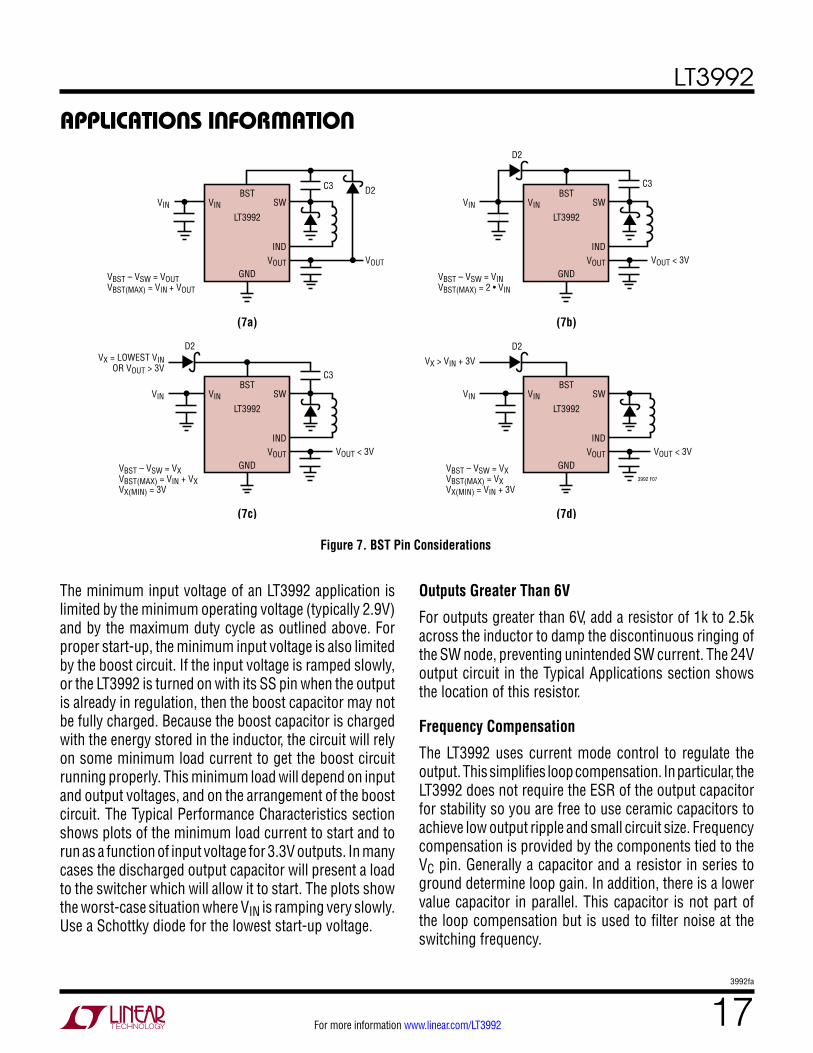
BST Pin Considerations
The capacitor and diode tied to the BST pin generate a voltage that is higher than the input voltage. In most cases a 0.47µF capacitor and a small Schottky diode (such as the BAT41) will work well. To ensure optimal performance at duty cycles greater than 80%, use a 0.5A Schottky diode (such as a MBR0560). Almost any type of film or ceramic capacitor is suitable, but the ESR should be <1Ω to ensure it can be fully recharged during the off time of the switch. The capacitor value can be approximated by:
CBST =
IOUT(MAX) • VOUT
5 • VIN VOUT – 2( ) • f
where IOUT(MAX) is the maximum load current.
Figure 7 shows four ways to arrange the boost circuit. The BST pin must be more than 3V above the SW pin for full efficiency. Generally, for outputs of 3.3V and higher the standard circuit (Figure 7a) is the best. For lower output voltages the boost diode can be tied to the input (Fig-ure 7b). The circuit in Figure 7a is more efficient because the BST pin current comes from a lower voltage source. Figure 7c shows the boost voltage source from available DC sources that are greater than 3V. The highest efficiency is attained by choosing the lowest boost voltage above 3V. For example, if you are generating 3.3V and 1.8V and the 3.3V is on whenever the 1.8V is on, the 1.8V boost diode can be connected to the 3.3V output. In any case, you must also be sure that the maximum voltage at the BST pin is less than the maximum specified in the Absolute Maximum Ratings section.
The boost circuit can also run directly from a DC voltage that is higher than the input voltage by more than 3V, as in Figure 7d. The diode is used to prevent damage to the LT3992 in case VX is held low while VIN is present. The circuit saves several components (both BST pins can be tied to D2). However, efficiency may be lower and dissipa-tion in the LT3992 may be higher. Also, if VX is absent, the LT3992 will still attempt to regulate the output, but will do so with very low efficiency and high dissipation because the switch will not be able to saturate, dropping 1.5V to 2V in conduction.
LT3992
173992fa
For more information www.linear.com/LT3992
applicaTions inForMaTion
Figure 7. BST Pin Considerations
The minimum input voltage of an LT3992 application is limited by the minimum operating voltage (typically 2.9V) and by the maximum duty cycle as outlined above. For proper start-up, the minimum input voltage is also limited by the boost circuit. If the input voltage is ramped slowly, or the LT3992 is turned on with its SS pin when the output is already in regulation, then the boost capacitor may not be fully charged. Because the boost capacitor is charged with the energy stored in the inductor, the circuit will rely on some minimum load current to get the boost circuit running properly. This minimum load will depend on input and output voltages, and on the arrangement of the boost circuit. The Typical Performance Characteristics section shows plots of the minimum load current to start and to run as a function of input voltage for 3.3V outputs. In many cases the discharged output capacitor will present a load to the switcher which will allow it to start. The plots show the worst-case situation where VIN is ramping very slowly. Use a Schottky diode for the lowest start-up voltage.
Outputs Greater Than 6V
For outputs greater than 6V, add a resistor of 1k to 2.5k across the inductor to damp the discontinuous ringing of the SW node, preventing unintended SW current. The 24V output circuit in the Typical Applications section shows the location of this resistor.
Frequency Compensation
The LT3992 uses current mode control to regulate the output. This simplifies loop compensation. In particular, the LT3992 does not require the ESR of the output capacitor for stability so you are free to use ceramic capacitors to achieve low output ripple and small circuit size. Frequency compensation is provided by the components tied to the VC pin. Generally a capacitor and a resistor in series to ground determine loop gain. In addition, there is a lower value capacitor in parallel. This capacitor is not part of the loop compensation but is used to filter noise at the switching frequency.
VINVIN
VX > VIN + 3V
BST
GND
LT3992
SW
INDVOUT
VBST – VSW = VXVBST(MAX) = VXVX(MIN) = VIN + 3V
VOUT < 3V
3992 F07
VINVIN
VX = LOWEST VINOR VOUT > 3V
BST
GND
LT3992
SW
INDVOUT
VBST – VSW = VXVBST(MAX) = VIN + VXVX(MIN) = 3V
VOUT < 3V
C3
VINVINBST
D2
GND
(7d)(7c)
(7b)
LT3992
SW
INDVOUT
VBST – VSW = VINVBST(MAX) = 2 • VIN
VOUT < 3V
C3
VINVINBST D2
GND
(7a)
LT3992
SW
INDVOUT
VBST – VSW = VOUTVBST(MAX) = VIN + VOUT
VOUT
C3
D2D2
LT3992
183992fa
For more information www.linear.com/LT3992
applicaTions inForMaTionLoop compensation determines the stability and transient performance. Designing the compensation network is a bit complicated and the best values depend on the application and in particular the type of output capacitor. A practical approach is to start with one of the circuits in this data sheet that is similar to your application and tune the com-pensation network to optimize the performance. Stability should then be checked across all operating conditions, including load current, input voltage and temperature.
The LT1375 data sheet contains a more thorough discus-sion of loop compensation and describes how to test the stability using a transient load.
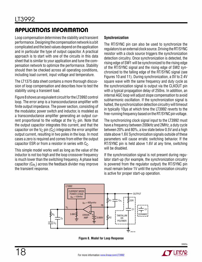
Figure 8 shows an equivalent circuit for the LT3992 control loop. The error amp is a transconductance amplifier with finite output impedance. The power section, consisting of the modulator, power switch and inductor, is modeled as a transconductance amplifier generating an output cur-rent proportional to the voltage at the VC pin. Note that the output capacitor integrates this current, and that the capacitor on the VC pin (CC) integrates the error amplifier output current, resulting in two poles in the loop. In most cases a zero is required and comes from either the output capacitor ESR or from a resistor in series with CC.
This simple model works well as long as the value of the inductor is not too high and the loop crossover frequency is much lower than the switching frequency. A phase lead capacitor (CPL) across the feedback divider may improve the transient response.
Synchronization
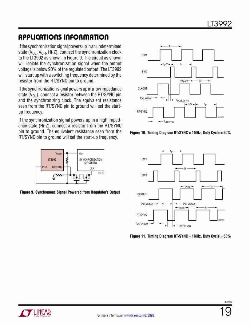
The RT/SYNC pin can also be used to synchronize the regulators to an external clock source. Driving the RT/SYNC resistor with a clock source triggers the synchronization detection circuitry. Once synchronization is detected, the rising edge of SW1 will be synchronized to the rising edge of the RT/SYNC signal and the rising edge of SW2 syn-chronized to the falling edge of the RT/SYNC signal (see Figures 10 and 11). During synchronization, a 0V to 2.4V square wave with the same frequency and duty cycle as the synchronization signal is output via the CLKOUT pin with a typical propagation delay of 250ns. In addition, an internal AGC loop will adjust slope compensation to avoid subharmonic oscillation. If the synchronization signal is halted, the synchronization detection circuitry will timeout in typically 10µs at which time the LT3992 reverts to the free-running frequency based on the RT/SYNC pin voltage.
The synchronizing clock signal input to the LT3992 must have a frequency between 200kHz and 2MHz, a duty cycle between 20% and 80%, a low state below 0.5V and a high state above 1.6V. Synchronization signals outside of these parameters will cause erratic switching behavior. If the RT/SYNC pin is held above 1.6V at any time, switching will be disabled.
If the synchronization signal is not present during regu-lator start-up (for example, the synchronization circuitry is powered from the regulator output) the RT/SYNC pin must remain below 1V until the synchronization circuitry is active for proper start-up operation.
Figure 8. Model for Loop Response
+
+–
0.806V
LT3992
FBVC
CF
CPL
OUTPUT
C1 C1
3992 F08
CC
RC
R1 ESR
TANTALUMOR
POLYMER
CERAMICR2
3.6M ERRORAMP
gm = 400µmho
CURRENT MODEPOWER STAGEgm = 4.8mho
LT3992
193992fa
For more information www.linear.com/LT3992
applicaTions inForMaTionIf the synchronization signal powers up in an undetermined state (VOL, VOH, Hi-Z), connect the synchronization clock to the LT3992 as shown in Figure 9. The circuit as shown will isolate the synchronization signal when the output voltage is below 90% of the regulated output. The LT3992 will start up with a switching frequency determined by the resistor from the RT/SYNC pin to ground.
If the synchronization signal powers up in a low impedance state (VOL), connect a resistor between the RT/SYNC pin and the synchronizing clock. The equivalent resistance seen from the RT/SYNC pin to ground will set the start-up frequency.
If the synchronization signal powers up in a high imped-ance state (Hi-Z), connect a resistor from the RT/SYNC pin to ground. The equivalent resistance seen from the RT/SYNC pin to ground will set the start-up frequency.
Figure 9. Synchronous Signal Powered from Regulator’s Output
Figure 10. Timing Diagram RT/SYNC = 1MHz, Duty Cycle = 50%
Figure 11. Timing Diagram RT/SYNC = 1MHz, Duty Cycle > 50%
LT3992 SYNCHRONIZATIONCIRCUITRY
VOUT1
RT/SYNC
3992 F09
VCC
CLKPG1
tP
tP
tP
tP/2
tP/2
tPtP/2tDCLKOSW2
tDRTSYNC
tDCLKOSW1
SW1
SW2
CLKOUT
RT/SYNC
3992 F10
tP
tDCLKOSW2tDCLKOSW1
SW1
SW2
CLKOUT
RT/SYNC
tDRTSYNCHtDRTSYNCH
3992 F11
tP
tPON
tPON
tP
tP
LT3992
203992fa
For more information www.linear.com/LT3992
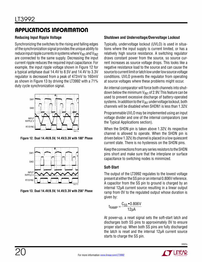
applicaTions inForMaTionReducing Input Ripple Voltage
Synchronizing the switches to the rising and falling edges of the synchronization signal provides the unique ability to reduce input ripple currents in systems where VIN1 and VIN2 are connected to the same supply. Decreasing the input current ripple reduces the required input capacitance. For example, the input ripple voltage shown in Figure 12 for a typical antiphase dual 14.4V to 8.5V and 14.4V to 3.3V regulator is decreased from a peak of 472mV to 160mV as shown in Figure 13 by driving the LT3992 with a 71% duty cycle synchronization signal.
Shutdown and Undervoltage/Overvoltage Lockout
Typically, undervoltage lockout (UVLO) is used in situa-tions where the input supply is current limited, or has a relatively high source resistance. A switching regulator draws constant power from the source, so source cur-rent increases as source voltage drops. This looks like a negative resistance load to the source and can cause the source to current limit or latch low under low source voltage conditions. UVLO prevents the regulator from operating at source voltages where these problems might occur.
An internal comparator will force both channels into shut-down below the minimum VIN1 of 2.9V. This feature can be used to prevent excessive discharge of battery-operated systems. In addition to the VIN1 undervoltage lockout, both channels will be disabled when SHDN1 is less than 1.32V.
Programmable UVLO may be implemented using an input voltage divider and one of the internal comparators (see the Typical Applications section).
When the SHDN pin is taken above 1.32V, its respective channel is allowed to operate. When the SHDN pin is driven below 1.32V, its channel is placed in a low quiescent current state. There is no hysteresis on the SHDN pins.
Keep the connections from any series resistors to the SHDN pins short and make sure that the interplane or surface capacitance to switching nodes is minimized.
Soft-Start
The output of the LT3992 regulates to the lowest voltage present at either the SS pin or an internal 0.806V reference. A capacitor from the SS pin to ground is charged by an internal 12µA current source resulting in a linear output ramp from 0V to the regulated output whose duration is given by:
tRAMP = CSS •0.806V
12µA
At power-up, a reset signal sets the soft-start latch and discharges both SS pins to approximately 0V to ensure proper start-up. When both SS pins are fully discharged the latch is reset and the internal 12µA current source starts to charge the SS pin.
Figure 12. Dual 14.4V/8.5V, 14.4V/3.3V with 180° Phase
Figure 13. Dual 14.4V/8.5V, 14.4V/3.3V with 256° Phase
SW1
SW2
RT/SYNC
3992 F12
INPUTRIPPLE V
SW1
SW2
RT/SYNC
INPUTRIPPLE V
3992 F13
LT3992
213992fa
For more information www.linear.com/LT3992
applicaTions inForMaTionWhen the SS pin voltage is below 110mV, the VC pin is pulled low which disables switching. This allows the SS pin to be used as an individual shutdown for each channel.
As the SS pin voltage rises above 110mV, the VC pin is released and the output is regulated to the SS voltage. When the SS pin voltage exceeds the internal 0.806V reference, the output is regulated to the reference. The SS pin voltage will continue to rise until it is clamped at typically 2.15V.
In the event of a VIN1 undervoltage lockout, the soft-start latch is set for both channels, triggering a full start-up sequence. If a channel’s SHDN pin is driven below 1.32V, its overvoltage lockout is enabled, or the internal die temperature for its power switch exceeds its maximum rating during normal operation, the soft-start latch is set for that channel.
In addition, if the load exceeds the maximum output switch current, the output will start to drop causing the VC pin clamp to be activated. As long as the VC pin is clamped, the SS pin will be discharged. As a result, the output will be regulated to the highest voltage that the maximum output current can support. For example, if a 6V output is loaded by 1Ω the SS pin will drop to 0.46V, regulating the output at 4.6V ( 4.6A • 1Ω ). Once the overload condition is removed, the output will soft start from the temporary voltage level to the normal regulation point.
Since the SS pin is clamped at typically 2.15V and has to discharge to 0.806V before taking control of regulation, momentary overload conditions will be tolerated without a soft-start recovery. The typical time before the SS pin takes control is:
tSS(CONTROL) =
CSS •1.2V0.9mA
Open-Collector Comparators
The CMPO pin is the open-collector output of an internal comparator. The comparator compares the CMPI pin volt-age to 90% of the reference voltage (0.72V) with 80mV of hysteresis.
The CMPO pin has a typical sink capability of 250µA when the CMPI pin is below the threshold and can withstand 60V
when the threshold is exceeded. The CMPO pin is active (sink capability is reduced in shutdown and undervoltage lockout mode) as long as the VIN1 pin voltage exceeds typically 2.9V.
The comparators can be used to monitor input and output voltages as well as die temperature. See the Typical Ap-plications circuit collection for examples.
Output Tracking/Sequencing
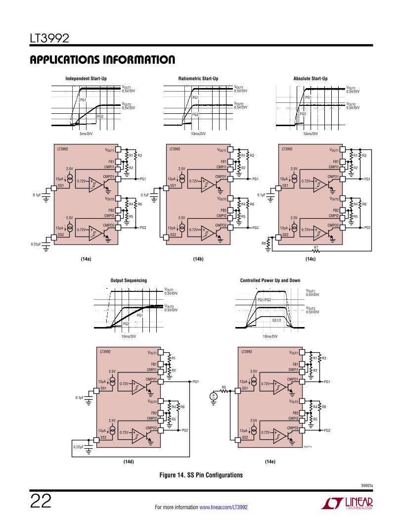
Complex output tracking and sequencing between channels can be implemented using the LT3992’s SS and CMPO pins. Figure 14 shows several configurations for output tracking/sequencing for a 3.3V and 1.8V application.
Independent soft-start for each channel is shown in Fig-ure 14a. The output ramp time for each channel is set by the soft-start capacitor as described in the soft-start section.
Ratiometric tracking is achieved in Figure 14b by con-necting both SS pins together. In this configuration, the SS pin source current is doubled (24µA) which must be taken into account when calculating the output rise time.
By connecting a feedback network from VOUT1 to the SS2 pin with the same ratio that sets VOUT2 voltage, absolute tracking shown in Figure 14c is implemented. The mini-mum value of the top feedback resistor (R1) should be set such that the SS pin can be driven all the way to ground with 0.9mA of sink current when VOUT1 is at its regulated voltage. In addition, a small VOUT2 voltage offset will be present due to the SS2 12µA source current. This offset can be corrected for by slightly reducing the value of R2.
Figure 14d illustrates output sequencing. When VOUT1 is within 10% of its regulated voltage, CMPO1 releases the SS2 soft-start pin allowing VOUT2 to soft-start. In this case CMPO1 will be pulled up to 2V by the SS pin. If a greater voltage is needed for CMPO1 logic, a pull-up resistor to VOUT1 can be used. This will decrease the soft-start ramp time and increase tolerance to momentary shorts.
If precise output ramp up and down is required, drive the SS pins as shown in Figure 14e. The minimum value of resistor (R3) should be set such that the SS pin can be driven all the way to ground with 0.9mA of sink current during power-up and fault conditions.
LT3992
223992fa
For more information www.linear.com/LT3992
applicaTions inForMaTion
Figure 14. SS Pin Configurations
+–
VOUT1
FB1CMPI1
CMPO1
LT3992
SS1
0.1µF
0.22µF
0.72V
2.5V
12µA
R1
R2
PG1
PG2
R3
5ms/DIV
Independent Start-Up
(14a)
VOUT10.5V/DIV
VOUT20.5V/DIV
+–
VOUT2
FB2CMPI2
CMPO20.72V
R4
R5
R6
SS2
2.5V
12µA
PG1
PG2
+–
VOUT1
FB1CMPI1
CMPO1
LT3992
SS1
0.1µF
0.22µF
0.72V
2.5V
12µA
R1
R2
PG1
PG2
10ms/DIV
Output Sequencing
(14d)
VOUT10.5V/DIV
VOUT20.5V/DIV
+–
VOUT2
FB2CMPI2
CMPO20.72V
R4
R5
R6
SS2
2.5V
12µA
PG1
PG2
+–
VOUT1
FB1CMPI1
CMPO1
LT3992
SS1R50.72V
2.5V
12µA
R1
R2
R3
PG1
10ms/DIV
Controlled Power Up and Down
(14e)
VOUT10.5V/DIV
VOUT20.5V/DIV
+–
VOUT2
FB2CMPI2
CMPO20.72V
R4
R5
3992 F14
R6
PG2
SS2
2.5V
12µA
PG1/PG2
SS1/2
+–
VOUT1
FB1CMPI1
CMPO1
LT3992
SS1
0.1µF
0.72V
2.5V
12µA
R1
R2
R3
PG1
PG2
10ms/DIV
Ratiometric Start-Up
(14b)
VOUT10.5V/DIV
VOUT20.5V/DIV
+–
VOUT2
FB2CMPI2
CMPO20.72V
R4
R5
R6
SS2
2.5V
12µA
PG1
PG2
+–
VOUT1
FB1CMPI1
CMPO1
LT3992
SS1
0.1µF
R8R7
0.72V
2.5V
12µA
R1
R2
R3
PG1
PG2
10ms/DIV
Absolute Start-Up
(14c)
VOUT10.5V/DIV
VOUT20.5V/DIV
+–
VOUT2
FB2CMPI2
CMPO20.72V
R4
R5
R6
SS2
2.5V
12µA
PG1
PG2
+–
LT3992
233992fa
For more information www.linear.com/LT3992
Application Optimization
In multiple channel applications requiring large VIN to VOUT ratios, the maximum frequency and resulting in-ductor size is determined by the channel with the largest ratio. The LT3992’s multi-frequency operation allows the user to minimize component size for each channel while maintaining constant frequency operation. The circuit in Figure 15 illustrates this approach. A 2-stage step-down approach coupled with multi-frequency operation will further reduce external component size by allowing an increase in frequency for the channel with the lower VIN to VOUT ratio. The drawback to this approach is that the output power capability for the first stage is determined by the output power drawn from the second stage. The dual step-down application in Figure 16 steps down the input voltage (VIN1) to the highest output voltage then uses that voltage to power the second output (VIN2). VOUT1 must be able to provide enough current for its output plus VOUT2 maximum load. Note that the VOUT1 voltage must be above VIN2’s minimum input voltage as specified in the Electrical Characteristics (typically 2.9V) when the second channel starts to switch. Delaying channel 2 can be accomplished by either independent soft-start capacitors or sequencing with the CMP01 output.
For example, assume a maximum input of 60V:
VIN = 60V, VOUT1 = 3.3V at 1.5A and VOUT2 = 12V at 1.5A.
Frequency(Hz)= VOUT +VDVIN – VSW +VD
•1
tON(MIN)
L =VIN – VOUT( ) • VOUT
VIN • f
Single Step-Down:
Frequency(Hz)= 3.3+0.660V – 0.4+0.6
•1
180ns≅ 350kHz
L1=60V – 3.3( ) •3.360V •350kHz
≥9µH
L2=60V –12( ) •1260V •350kHz
≥27µH
2-Stage Step-Down:
Frequency(Hz)= 12+0.660V – 0.4+0.6
•1
180ns≅1MHz
L1=60V –12( ) •1260V •1MHz
≥10µH
L2=12– 3.3( ) •3.3
12 •1MHz≥2.4µH
2-Stage Step-Down Multi-Frequency:
RDIV = 61.9k, FREQ1 = 900kHz, FREQ2 = 1800kHz.
L1=60V –12( ) •1260V •900kHz
≥11µH
L2=12– 3.3( ) •3.312 •1800kHz
≥1.3µH
In addition, RILIM2 = 52.3k reduces the peak current limit on Channel 2 to 2.5A, which reduces inductor size and catch diode requirements.
applicaTions inForMaTion

LT3992
243992fa
For more information www.linear.com/LT3992
Figure 15. 12V and 3.3V Dual Step-Down Multi-Frequency Converter
applicaTions inForMaTion
BST1
SW1
VOUT1
CMPI1
CMPO1
SS1ILIM1 ILIM1
RT/SYNC
DIV
VC1
FB1
IND1
SW2
VOUT2
CMPI2
CMPO2
SS2ILIM2
CLKOUT
VC2
TJ
FB2
IND2
3992 F15
BST2
SHDN1 SHDN2
VIN1
LT3992
GND
VIN2
4.7µF 4.7µF
VIN115V TO 60V
VOUT212V1.5A400kHz
VOUT1
VOUT13.3V1.5A
200kHz100k
PG1
22µH 22µH0.47µF 0.22µF
8.06k
61.9k13k60.4k
1000pF33pF0.1µF
10k
680pF0.1µF
33pF15k
113k
10nF
CLKOUT400kHz
8.06k24.9k100µF
×2 47µF100k
PG2
Figure 16. 12V and 3.3V 2-Stage Multi-Frequency Step-Down Converter
BST1
SW1
VOUT1
CMPI1
CMPO1
SS1ILIM1 ILIM1
RT/SYNC
DIV
VC1
FB1
IND1
SW2
VOUT2
CMPI2
CMPO2
SS2ILIM2
CLKOUT
VC2
TJ
FB2
IND2
3992 F16
BST2
SHDN1 SHDN2
VIN1VOUT2
LT3992
GND
VIN2
4.7µF
VIN115V TO 60V
VOUT23.3V2A1600kHz
VOUT112V1A
400kHz100k
PG
22µH 2.2µH0.1µF 0.1µF
8.06k
102k15k60.4k
680pF33pF
0.1µF
48.7k
470pF 0.1µF33pF
16k
24.9k
FB1
10nF
CLKOUT1600kHz
8.06k 113k10µF 47µF

LT3992
253992fa
For more information www.linear.com/LT3992
applicaTions inForMaTion
Figure 17. Diode D4 Prevents a Shorted Input from Discharging a Backup Battery Tied to the Output
Figure 18. Subtracting the Current When the Switch Is On (18a) from the Current When the Switch Is Off (18b) Reveals the Path of the High Frequency Switching Current (18c). Keep this Loop Small. The Voltage on the SW and BST Traces Will Also Be Switched; Keep These Traces As Short As Possible. Finally, Make Sure the Circuit Is Shielded with a Local Ground Plane
Shorted and Reverse Input Protection
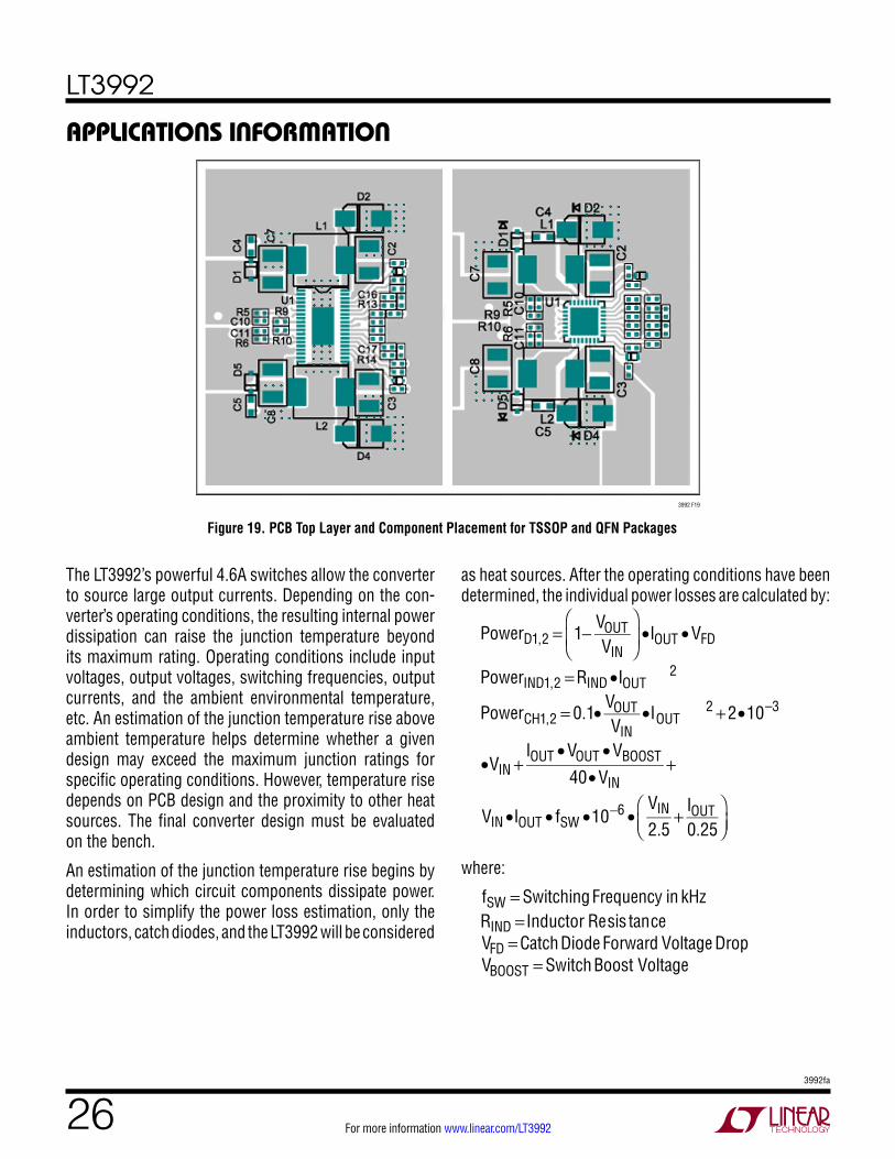
If the inductor is chosen so that it won’t saturate exces-sively, an LT3992 step-down regulator will tolerate a shorted output. There is another situation to consider in systems where the output will be held high when the input to the LT3992 is absent. This may occur in battery charging applications or in battery back-up systems where a battery or some other supply is diode OR-ed with the LT3992’s output. If the VIN1/2 pin is allowed to float and the SHDN pin is held high (either by a logic signal or because it is tied to VIN), then the LT3992’s internal circuitry will pull its quiescent current through its SW pin. This is fine if your system can tolerate a few mA in this state. If you ground the SHDN pin, the SW pin current will drop to essentially zero. However, if the VIN pin is grounded while the output is held high, then parasitic diodes inside the LT3992 can pull large currents from the output through the SW pin and the VIN1/2 pin. Figure 17 shows a circuit that will run only when the input voltage is present and that protects against a shorted or reversed input.
VIN
GND
(18a)
LT3992 SW
VIN
GND
(18c)
LT3992 SW
3992 F18
VIN
GND
(18b)
LT3992 SW
VINVIN1/2 VOUT1/2
SW
LT3992
D4
PARASITIC DIODE
3992 F17
PCB Layout
For proper operation and minimum EMI, care must be taken during printed circuit board (PCB) layout. Figure 18 shows the high di/dt paths in the buck regulator circuit. Note that large switched currents flow in the power switch, the catch diode and the input capacitor. The loop formed by these components should be as small as possible.
These components, along with the inductor and output capacitor, should be placed on the same side of the cir-cuit board and their connections should be made on that layer. Place a local, unbroken ground plane below these components, and tie this ground plane to system ground
at one location, ideally at the ground terminal of the out-put capacitor C2. Route all small signal analog returns to the ground connection at the bottom of the package. Additionally, the SW and BST traces should be kept as short as possible.
Thermal Considerations
The PCB must also provide heat sinking to keep the LT3992 cool. The exposed metal on the bottom of the package must be soldered to a ground plane. This ground should be tied to other copper layers below with thermal vias; these layers will spread the heat dissipated by the LT3992. Place additional vias near the catch diodes. Adding more copper to the top and bottom layers and tying this copper to the internal planes with vias can further reduce thermal resistance. The topside metal and component outlines in Figure 19 illustrate proper component placement and trace routing.
LT3992
263992fa
For more information www.linear.com/LT3992
applicaTions inForMaTion
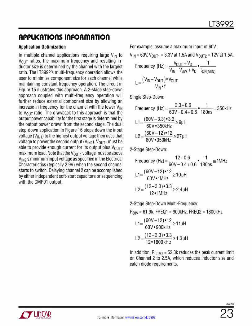
The LT3992’s powerful 4.6A switches allow the converter to source large output currents. Depending on the con-verter’s operating conditions, the resulting internal power dissipation can raise the junction temperature beyond its maximum rating. Operating conditions include input voltages, output voltages, switching frequencies, output currents, and the ambient environmental temperature, etc. An estimation of the junction temperature rise above ambient temperature helps determine whether a given design may exceed the maximum junction ratings for specific operating conditions. However, temperature rise depends on PCB design and the proximity to other heat sources. The final converter design must be evaluated on the bench.
An estimation of the junction temperature rise begins by determining which circuit components dissipate power. In order to simplify the power loss estimation, only the inductors, catch diodes, and the LT3992 will be considered
Figure 19. PCB Top Layer and Component Placement for TSSOP and QFN Packages
3992 F19
as heat sources. After the operating conditions have been determined, the individual power losses are calculated by:
PowerD1,2 = 1− VOUTVIN
⎛
⎝⎜
⎞
⎠⎟ •IOUT •VFD
PowerIND1,2 =RIND•IOUT2
PowerCH1,2 = 0.1• VOUTVIN
•IOUT2 +2•10–3
•VIN +IOUT •VOUT •VBOOST
40•VIN+
VIN•IOUT • fSW •10−6 •VIN
2.5+ IOUT
0.25⎛⎝⎜
⎞⎠⎟
where:
fSW =SwitchingFrequency in kHzRIND = Inductor Resis tanceVFD =CatchDiode Forward Voltage DropVBOOST =SwitchBoost Voltage

LT3992
273992fa
For more information www.linear.com/LT3992
applicaTions inForMaTionFor the LT3992 demo board using the TSSOP package, the estimated junction temperature rise above ambient temperature is found by:
TRISETSSOP ≈10•(PowerD1+PowerD2)+12.3•(PowerIND1+Power IND2)+17.5•
PowerCH1+PowerCH2( )The estimated junction temperature rise above ambient for the LT3992 QFN layout is:
TRISEQFN ≈8.5•(Power D1+Power D2)+13•(Power IND1+Power IND2)+23•PowerCH1+PowerCH2( )
For example, the typical application circuits listed in Table 4 are used to calculate the individual power loss contribu-tions in Table 5. Table 6 shows the estimated power loss and junction temperature rise above ambient temperature. Note that the larger TSSOP package demonstrates better thermal performance than the compact QFN package on the LT3992 demo circuit boards. For LT3992 applications that favor thermal performance, the TSSOP package is the preferred package option.
Table 4
APPLICATIONVIN1 (V)
VIN2 (V)
fSW CH1
fSW CH2
VOUT1 (V)
IOUT1 (A)
VOUT2 (V)
IOUT2 (A)
Front Page 48 12 400 1600 12 1.5 5 2
Back Page 48 48 300 300 5 2 3 2
Table 5
APPLICATIONPD1 (W)
PD2 (W)
PL1 (W)
PL2 (W)
PCH1 (W)
PCH2 (W)
Front Page 0.54 0.56 0.23 0.28 0.99 0.79
Back Page 0.88 0.92 0.28 0.2 0.95 0.91
Table 6PLOSS (W) TRISE TSSOP (°C) TRISE QFN (°C)
APPLICATION CALC MEAS CALC MEAS CALC MEAS
Front Page 3.38 3.2 48.3 46.1 56.8 53.3
Back Page 4.14 4.2 56.4 53.0 64.3 62.9
The power loss and temperature rise equations provided in the Thermal Considerations section serve as a good starting point for estimating the junction temperature
rise. However, the LT3992 is a very versatile converter. The combination of independent input voltages, output voltages, output currents, switching frequencies, and package selections for the LT3992 dictate that no power loss estimation scheme can accommodate every possible operating condition. As such, it is absolutely necessary to evaluate a converter’s performance at the bench.
The power dissipation in the other power components such as boost diodes, input and output capacitors, inductor core loss, and trace resistances cause additional copper heating and can further increase what the IC sees as am-bient temperature. See the LT1767 data sheet’s Thermal Considerations section.
Die Temperature and Thermal Shutdown
The LT3992 TJ pin outputs a voltage proportional to the internal junction temperature. The TJ pin typically outputs 250mV for 25°C and has a slope of 10mV/°C. Without the aid of external circuitry, the TJ pin output is valid from 20°C to 150°C (200mV to 1.5V) with a maximum load of 100µA.
Full Temperature Range Measurement
To extend the operating temperature range of the TJ out-put below 20°C, connect a resistor from the TJ pin to a negative supply as shown in Figure 20. The negative rail voltage and TJ pin resistor may be calculated using the following equations:
VNEG ≤ 2 •TEMP(MIN)°C100
R1≤| VNEG |33µA
where:
TEMP(MIN)°C is the minimum temperature where a valid TJ pin output is required.
VNEG = Regulated negative voltage supply.
For example:
TEMP(MIN)°C = –40°C
VNEG ≤ –0.8V
VNEG = –1, R1 ≤ |VNEG|/33µA = 30.2kΩ
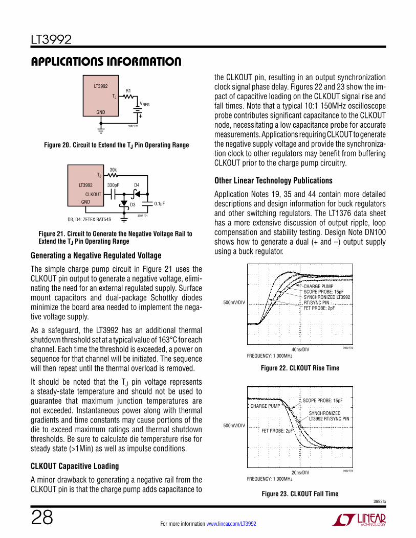
LT3992
283992fa
For more information www.linear.com/LT3992
applicaTions inForMaTion
Generating a Negative Regulated Voltage
The simple charge pump circuit in Figure 21 uses the CLKOUT pin output to generate a negative voltage, elimi-nating the need for an external regulated supply. Surface mount capacitors and dual-package Schottky diodes minimize the board area needed to implement the nega-tive voltage supply.
As a safeguard, the LT3992 has an additional thermal shutdown threshold set at a typical value of 163°C for each channel. Each time the threshold is exceeded, a power on sequence for that channel will be initiated. The sequence will then repeat until the thermal overload is removed.
It should be noted that the TJ pin voltage represents a steady-state temperature and should not be used to guarantee that maximum junction temperatures are not exceeded. Instantaneous power along with thermal gradients and time constants may cause portions of the die to exceed maximum ratings and thermal shutdown thresholds. Be sure to calculate die temperature rise for steady state (>1Min) as well as impulse conditions.
CLKOUT Capacitive Loading
A minor drawback to generating a negative rail from the CLKOUT pin is that the charge pump adds capacitance to
Figure 20. Circuit to Extend the TJ Pin Operating Range
Figure 21. Circuit to Generate the Negative Voltage Rail to Extend the TJ Pin Operating Range
the CLKOUT pin, resulting in an output synchronization clock signal phase delay. Figures 22 and 23 show the im-pact of capacitive loading on the CLKOUT signal rise and fall times. Note that a typical 10:1 150MHz oscilloscope probe contributes significant capacitance to the CLKOUT node, necessitating a low capacitance probe for accurate measurements. Applications requiring CLKOUT to generate the negative supply voltage and provide the synchroniza-tion clock to other regulators may benefit from buffering CLKOUT prior to the charge pump circuitry.
Other Linear Technology Publications
Application Notes 19, 35 and 44 contain more detailed descriptions and design information for buck regulators and other switching regulators. The LT1376 data sheet has a more extensive discussion of output ripple, loop compensation and stability testing. Design Note DN100 shows how to generate a dual (+ and –) output supply using a buck regulator.
Figure 22. CLKOUT Rise Time
Figure 23. CLKOUT Fall Time
LT3992
30k
330pF
0.1µF
D3, D4: ZETEX BAT54S
D4
D3GND
3992 F21
TJ
CLKOUT
500mV/DIV
40ns/DIV 3992 F22
FREQUENCY: 1.000MHz
CHARGE PUMPSCOPE PROBE: 15pFSYNCHRONIZED LT3992RT/SYNC PINFET PROBE: 2pF
500mV/DIV
20ns/DIV 3992 F23
FREQUENCY: 1.000MHz
CHARGE PUMPSCOPE PROBE: 15pF
FET PROBE: 2pF
SYNCHRONIZEDLT3992 RT/SYNC PIN
+
LT3992R1
VNEG
GND
3992 F20
TJ

LT3992
293992fa
For more information www.linear.com/LT3992
Typical applicaTions
Quad
Out
put 5
V, 2
.5V,
1.8
V an
d 1.
2V M
ulti-
Freq
uenc
y Sy
nchr
oniz
ed, 2
-Sta
ge
Conv
erte
r with
Out
put S
eque
ncin
g, A
bsol
ute
Trac
king
and
Cur
rent
Lim
iting
BST1
SW1
V OUT
1
CMPI
1
CMPO
1
SS1
ILIM
1V C
1
RT/S
YNC
DIV
FB1
IND1
SW2
V OUT
2
CMPI
2
CMPO
2
SS2
ILIM
2V C
2
CLKO
UT T JFB2
IND2
0.47
µF
4.7µ
F
1µF
1µF
1µF
47µF
42.2
k
0.1µ
F
1000
pF33
pF
470p
F
33pF
10nF
8.06
k
8.06
k
34.8
k
102k
11.8
k16
.9k
42.2
k8.
06k
CLOC
KOUT
1200
kHz
10k
8.06
k
4.02
k
100k
V IN
7V T
O 60
V
V OUT
15V
1.5A
300k
Hz
15µH
BST2
SHDN
1SH
DN2
V IN1
LT39
92
GND
V IN2
0.1µ
F
100p
F
0.1µ
F
47µF
100k
16.9
k
V OUT
22.
5V 1A12
00kH
z
PG
2.2µ
H
BST1
SW1
V OUT
1
CMPI
1
CMPO
1
SS1
ILIM
1V C
1
RT/S
YNC
DIV
FB1
IND1
SW2
V OUT
2
CMPI
2
CMPO
2
SS2
ILIM
2V C
2
CLKO
UT T JFB2
IND2
0.1µ
F
4.02
k10
0pF
100µ
F
470p
F
33pF
470p
F
33pF
10nF
8.06
k8.
06k
10k
15k
42.2
k
3992
TA0
2
42.2
k
V OUT
31.
2V 1A12
00kH
z
2.2µ
H
BST2
SHDN
1SH
DN2
V IN1
LT39
92
GND
V IN2
0.1µ
F
100p
F47
µF10
k
V OUT
41.
8V1A 12
00kH
z
2.2µ
H
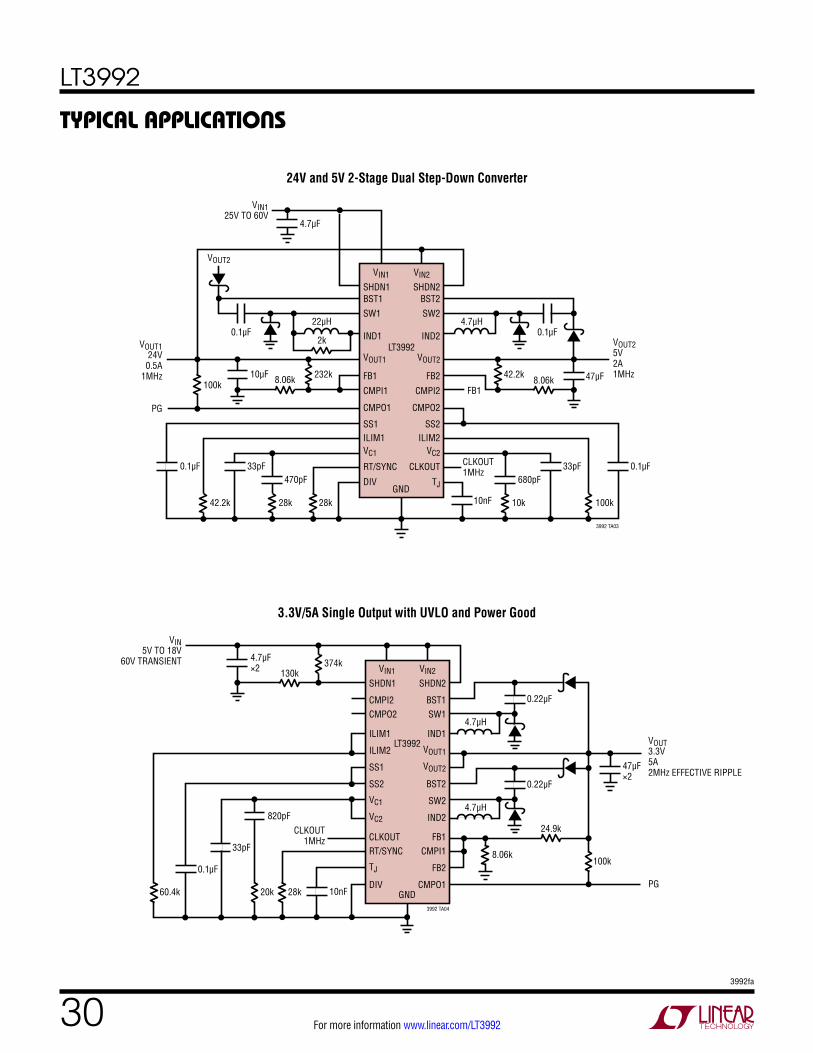
LT3992
303992fa
For more information www.linear.com/LT3992
Typical applicaTions
24V and 5V 2-Stage Dual Step-Down Converter
BST1
SW1
VOUT1
CMPI1
CMPO1
SS1ILIM1
RT/SYNC
DIV
VC1
FB1
IND1
SW2
VOUT2
CMPI2
CMPO2
SS2ILIM2
CLKOUT
VC2
TJ
FB2
IND2
3992 TA03
BST2SHDN1 SHDN2
VIN1
VOUT2
LT3992
GND
VIN2
4.7µF
VIN125V TO 60V
VOUT25V2A1MHz
VOUT124V0.5A
1MHz100k
PG
22µH 4.7µH0.1µF 0.1µF
8.06k
28k42.2k
470pF33pF0.1µF
28k
680pF0.1µF33pF
100k10k
42.2k
FB1
10nF
CLKOUT1MHz
8.06k 232k10µF
2k
47µF
3.3V/5A Single Output with UVLO and Power Good
SW1
VOUT1
CMPO1
CMPI1
SS1
ILIM1
VC1
RT/SYNC
DIV
FB1
IND1
SW2
VOUT2
CMPI2CMPO2
SS2
ILIM2
VC2
CLKOUTCLKOUT
1MHz
TJ FB2
IND2
4.7µF×2
820pF
10nF
33pF
0.1µF
28k20k60.4k
3992 TA04
VIN5V TO 18V
60V TRANSIENT
BST1
BST2
SHDN1 SHDN2
VIN1
LT3992
GND
VIN2
0.22µF
47µF×2
100k
PG
8.06k
24.9k
VOUT3.3V5A2MHz EFFECTIVE RIPPLE
4.7µH
0.22µF
4.7µH
130k374k

LT3992
313992fa
For more information www.linear.com/LT3992
Typical applicaTions
Power Supply Dual Input Single 3.3V/4A Output Step-Down Converter
5V and 1.8V Dual 2-Stage Converter
SW1
VOUT1
CMPO1
CMPI1
LIM1
SS1
VC1
RT/SYNC
TJ
FB1
IND1
SW2
VOUT2
CMPI2CMPO2
LIM2
SS2
VC2
CLKOUTCLKOUT
2MHz
DIV FB2
IND2
4.7µF
680pF
10nF
33pF0.1µF
61.9k
61.9k21k
42.2k
64.9k
3992 TA05
VIN112V
BST1
BST2
SHDN1 SHDN1SHDN2
VIN1
LT3992
GND
VIN2
0.22µF
47µF
8.06k
24.9k
VOUT3.3V4A
VIN25V
2.2µH
0.22µF
2.2µH
13k
47.5k1µF
BST1
SW1
VOUT1
CMPI1
CMPO1
SS1
ILIM1 ILIM1VC1
RT/SYNC
DIV
FB1
FB1
IND1
SW2
VOUT2
CMPI2
CMPO2
SS2
ILIM2VC2
CLKOUTCLOCKOUT1600kHz
TJ
FB2
IND20.22µF
4.7µF
42.2k
100k
22µF
0.1µF
820pF
33pF
33pF
10nF
8.06k 8.06k
48.7k 102k13k
0.1µF
3992 TA06
21k
470pF
21k
VIN17V TO 60V
VOUT15V1A
400kHz
PG
15µH
BST2SHDN1 SHDN2
VIN1
LT3992
GND
VIN2
0.22µF
100pF 47µF10k
VOUT21.8V1A1600kHz
2.2µH
1µF

LT3992
323992fa
For more information www.linear.com/LT3992
Typical applicaTions
12V,
3.3
V an
d 1.
2V Tr
iple
Out
put w
ith E
xter
nal S
ynch
roni
zatio
n, O
utpu
t Seq
uenc
ing
and
Trac
king
SW1
V OUT
1
CMPO
1
CMPI
1
SS1
ILIM
1
V C1
RT/S
YNC
DIV
FB1
IND1
SW2
V OUT
2
CMPI
2
CMPO
2
SS2
ILIM
2
V C2
CLKO
UTCL
KOUT
1MHz
T J
FB2
IND2
2.2µ
F×2
1300
pF
10nF
33pF
0.1µ
F28
k
7.5k
22.1
k
3992
TA0
7
V IN
13V
TO 6
0V
BST2
SHDN
1
SHDN
2
BST1
V IN1
LT39
92
GND
V IN2
0.22
µF
22µF
×2
200k
PG
8.06
k11
3k
22µH
0.22
µF22
µH
0.1µ
F
133k
V+OU
T1
LTC6
908-
1
OUT2
MOD
GND
SET
BST1
SW1
V OUT
1
CMPI
1
CMPO
1
SS1
SS1
ILIM
1V C
1
RT/S
YNC
DIV
FB1
IND1
SW2
V OUT
2
CMPI
2
CMPO
2
SS2
ILIM
2V C
2
CLKO
UT T JFB2
IND2
0.1µ
F
1µF
4.02
k10
0µF
×210
0pF
0.1µ
F
1000
pF
33pF
470p
F
10nF
8.06
k8.
06k
61.9
k7.
68k
16k
100k
33pF
100k
V OUT
3
V OUT
21.
2V 3A50
0kHz
V OUT
2
V OUT
112
V0.
5A1M
Hz
2.2µ
H
BST2
SHDN
1SH
DN1
SHDN
1SH
DN2
V IN1
LT39
92
GND
V IN2
0.1µ
F
100p
F10
0µF
24.9
k
V OUT
33.
3V3A 1M
Hz
2.2µ
H
1µF
OFF
ON

LT3992
333992fa
For more information www.linear.com/LT3992
package DescripTion
4.75(.187)
REF
FE38 (AA) TSSOP REV C 0910
0.09 – 0.20(.0035 – .0079)
0° – 8°
0.25REF
0.50 – 0.75(.020 – .030)
4.30 – 4.50*(.169 – .177)
1 19
20
REF
9.60 – 9.80*(.378 – .386)
38
1.20(.047)MAX
0.05 – 0.15(.002 – .006)
0.50(.0196)
BSC0.17 – 0.27
(.0067 – .0106)TYP
RECOMMENDED SOLDER PAD LAYOUT
0.315 ±0.05
0.50 BSC
4.50 REF
6.60 ±0.10
1.05 ±0.10
4.75 REF
2.74 REF
2.74(.108)
MILLIMETERS(INCHES) *DIMENSIONS DO NOT INCLUDE MOLD FLASH. MOLD FLASH
SHALL NOT EXCEED 0.150mm (.006") PER SIDE
NOTE:1. CONTROLLING DIMENSION: MILLIMETERS2. DIMENSIONS ARE IN
3. DRAWING NOT TO SCALE
SEE NOTE 4
4. RECOMMENDED MINIMUM PCB METAL SIZE FOR EXPOSED PAD ATTACHMENT
6.40(.252)BSC
FE Package38-Lead Plastic TSSOP (4.4mm)
(Reference LTC DWG # 05-08-1772 Rev C)
Exposed Pad Variation AA
Please refer to http://www.linear.com/designtools/packaging/ for the most recent package drawings.
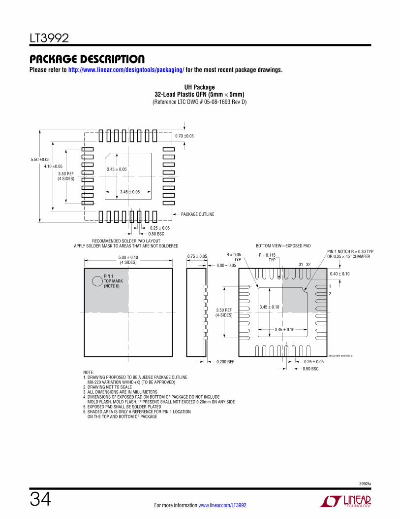
LT3992
343992fa
For more information www.linear.com/LT3992
package DescripTion
UH Package32-Lead Plastic QFN (5mm × 5mm)
(Reference LTC DWG # 05-08-1693 Rev D)
5.00 ± 0.10(4 SIDES)
NOTE:1. DRAWING PROPOSED TO BE A JEDEC PACKAGE OUTLINE M0-220 VARIATION WHHD-(X) (TO BE APPROVED)2. DRAWING NOT TO SCALE3. ALL DIMENSIONS ARE IN MILLIMETERS4. DIMENSIONS OF EXPOSED PAD ON BOTTOM OF PACKAGE DO NOT INCLUDE MOLD FLASH. MOLD FLASH, IF PRESENT, SHALL NOT EXCEED 0.20mm ON ANY SIDE5. EXPOSED PAD SHALL BE SOLDER PLATED6. SHADED AREA IS ONLY A REFERENCE FOR PIN 1 LOCATION ON THE TOP AND BOTTOM OF PACKAGE
PIN 1TOP MARK(NOTE 6)
0.40 ± 0.10
31
1
2
32
BOTTOM VIEW—EXPOSED PAD
3.50 REF(4-SIDES)
3.45 ± 0.10
3.45 ± 0.10
0.75 ± 0.05 R = 0.115TYP
0.25 ± 0.05(UH32) QFN 0406 REV D
0.50 BSC
0.200 REF
0.00 – 0.05
0.70 ±0.05
3.50 REF(4 SIDES)
4.10 ±0.05
5.50 ±0.05
0.25 ± 0.05
PACKAGE OUTLINE
0.50 BSC
RECOMMENDED SOLDER PAD LAYOUTAPPLY SOLDER MASK TO AREAS THAT ARE NOT SOLDERED
PIN 1 NOTCH R = 0.30 TYPOR 0.35 × 45° CHAMFERR = 0.05
TYP
3.45 ± 0.05
3.45 ± 0.05
Please refer to http://www.linear.com/designtools/packaging/ for the most recent package drawings.
LT3992
353992fa
For more information www.linear.com/LT3992
revision hisToryREV DATE DESCRIPTION PAGE NUMBER
A 04/13 Clarified Typical Switching FrequencyClarified Block DiagramClarified Figure 1 call out in last paragraphClarified Applications Information
31012
14, 16
Information furnished by Linear Technology Corporation is believed to be accurate and reliable. However, no responsibility is assumed for its use. Linear Technology Corporation makes no representa-tion that the interconnection of its circuits as described herein will not infringe on existing patent rights.
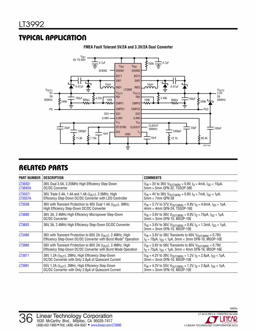
LT3992
363992fa
For more information www.linear.com/LT3992
relaTeD parTs
Typical applicaTionFMEA Fault Tolerant 5V/2A and 3.3V/2A Dual Converter
PART NUMBER DESCRIPTION COMMENTS
LT3692/LT3692A
36V, Dual 3.5A, 2.25MHz High Efficiency Step-Down DC/DC Converter
VIN = 3V to 36V, VOUT(MIN) = 0.8V, IQ = 4mA, ISD < 10µA, 5mm × 5mm QFN-32, TSSOP-38E
LT3507/LT3507A
36V, Triple 2.4A, 1.4A and 1.4A (IOUT), 2.5MHz, High Efficiency Step-Down DC/DC Converter with LDO Controller
VIN = 4V to 36V, VOUT(MIN) = 0.8V, IQ = 7mA, ISD = 1µA, 5mm × 7mm QFN-38
LT3508 36V with Transient Protection to 40V, Dual 1.4A (IOUT), 3MHz, High Efficiency Step-Down DC/DC Converter
VIN = 3.7V to 37V, VOUT(MIN) = 0.8V, IQ = 4.6mA, ISD = 1µA, 4mm × 4mm QFN-24, TSSOP-16E
LT3680 36V, 3A, 2.4MHz High Efficiency Micropower Step-Down DC/DC Converter
VIN = 3.6V to 36V, VOUT(MIN) = 0.8V, IQ = 75µA, ISD < 1µA, 3mm × 3mm DFN-10, MSOP-10E
LT3693 36V, 3A, 2.4MHz High Efficiency Step-Down DC/DC Converter VIN = 3.6V to 36V, VOUT(MIN) = 0.8V, IQ = 1.3mA, ISD < 1µA, 3mm × 3mm DFN-10, MSOP-10E
LT3480 36V with Transient Protection to 60V, 2A (IOUT), 2.4MHz, High Efficiency Step-Down DC/DC Converter with Burst Mode® Operation
VIN = 3.6V to 38V, Transients to 60V, VOUT(MIN) = 0.78V, IQ = 70µA, ISD < 1µA, 3mm × 3mm DFN-10, MSOP-10E
LT3980 58V with Transient Protection to 80V, 2A (IOUT), 2.4MHz, High Efficiency Step-Down DC/DC Converter with Burst Mode Operation
VIN = 3.6V to 58V, Transients to 80V, VOUT(MIN) = 0.79V, IQ = 75µA, ISD < 1µA, 3mm × 4mm DFN-16, MSOP-16E
LT3971 38V, 1.2A (IOUT), 2MHz, High Efficiency Step-Down DC/DC Converter with Only 2.8µA of Quiescent Current
VIN = 4.2V to 38V, VOUT(MIN) = 1.2V, IQ = 2.8µA, ISD < 1µA, 3mm × 3mm DFN-10, MSOP-10E
LT3991 55V, 1.2A (IOUT), 2MHz, High Efficiency Step-Down DC/DC Converter with Only 2.8µA of Quiescent Current
VIN = 4.2V to 55V, VOUT(MIN) = 1.2V, IQ = 2.8µA, ISD < 1µA, 3mm × 3mm DFN-10, MSOP-10E
BST1
SW1
VOUT1
CMPI1
CMPO1
SS1ILIM1
RT/SYNC
DIV
VC1
FB1
IND1
SW2
VOUT2
CMPI2
CMPO2
SS2ILIM2
SS2ILIM2
CLKOUT
VC2
TJ
FB2
IND2
3992 TA08
BST2
SHDN1 SHDN2SHDN2
VIN1
LT3992
GND
VIN2
4.7µF 4.7µF100k
VIN16V TO 60V
VOUT23.3V2A300kHz
VOUT15V2A
300kHz 249k
PG
15µH 10µH0.47µF 0.47µF
806Ω
11.8k
1000pF33pF 33pF
7.15k
1000pF100nF
60.4k12.1k
2.49k
10nF
CLKOUT300kHz
806Ω 4.22k100µF 100k 100k 100µF
10nF
249k
PG2
LINEAR TECHNOLOGY CORPORATION 2012
LT 0413 REV A • PRINTED IN USALinear Technology Corporation1630 McCarthy Blvd., Milpitas, CA 95035-7417(408) 432-1900 FAX: (408) 434-0507 www.linear.com/LT3992