lt8336 40v, 2.5a, low i synchronous step-up silent
TRANSCRIPT

LT8336
1Rev. A
For more information www.analog.comDocument Feedback
TYPICAL APPLICATION
FEATURES DESCRIPTION
40V, 2.5A, Low IQ Synchronous Step-Up Silent Switcher with PassThru
The LT®8336 is a low IQ, synchronous step-up DC/DC converter. It features Silent Switcher architecture and optional spread spectrum frequency modulation to min-imize EMI emissions while delivering high efficiencies at high switching frequencies.
The wide input/output voltage range, low VIN pin quies-cent current in Burst Mode operation, and 100% duty cycle capability for the synchronous MOSFET in PassThru operation (VIN ≥ VOUT), make the LT8336 ideally suited for general purpose step-up and automotive preboost applications.
The LT8336 integrates 40V, 2.5A power switches, operat-ing at a fixed switching frequency programmable between 300kHz and 3MHz and synchronizable to an external clock. Pulse-skipping or Burst Mode operation can be selected, with or without spread-spectrum frequency modulation, to optimize efficiency and EMI performance.
The LT8336 features output soft-start, an output power good flag and output overvoltage lockout.
High Efficiency 8V to 16V Input, 2MHz, 24V Output Boost Converter
APPLICATIONS
n Silent Switcher® Architecture n Ultralow EMI Emissions n Optional Spread Spectrum Frequency Modulation
n Integrated 40V, 2.5A Power Switches n Wide Input/Output Voltage Range: 2.7V to 40V n Low VIN Pin Quiescent Current:
n 0.3µA in Shutdown n 4µA in Burst Mode® Operation n 15µA in PassThru™ Operation
n 100% Duty Cycle Capability for Synchronous MOSFET n Adjustable and Synchronizable: 300kHz to 3MHz n Pulse-Skipping or Burst Mode Operation at Light Load n Output Soft-Start and Power Good Monitor n Internal Compensation n Accurate 1V Enable Pin Threshold n Small 16-Lead (3mm × 3mm) LQFN Package n AEC-Q100 Qualified for Automotive Applications
n Automotive and Industrial Power Supplies n General Purpose Step-Up All registered trademarks and trademarks are the property of their respective owners. Protected
by U.S patents, including 10686381.
Efficiency
OUTPUT CURRENT (mA)0.1 1 10 100 1k 10k
0
10
20
40
50
60
70
80
90
100
1
10
100
1k
10k
EFFI
CIEN
CY (%
)
POWER LOSS (m
W)
8336 TA01b
VIN = 16VVIN = 8V
Burst Mode OPERATIONINTVCC
SYNC/MODE
PG
VIN SW BST
EN/UVLO
FB
GND
VOUT
LT8336
8336 TA01a
RT
VIN8V TO 16V
VOUT24V0.6A AT 8V VIN1.2A AT 16V VIN
10µF
6.8µH
0.1µF
1M
10µF×2
43.2k
1µF47.5k2MHz
LT8336
2Rev. A
For more information www.analog.com
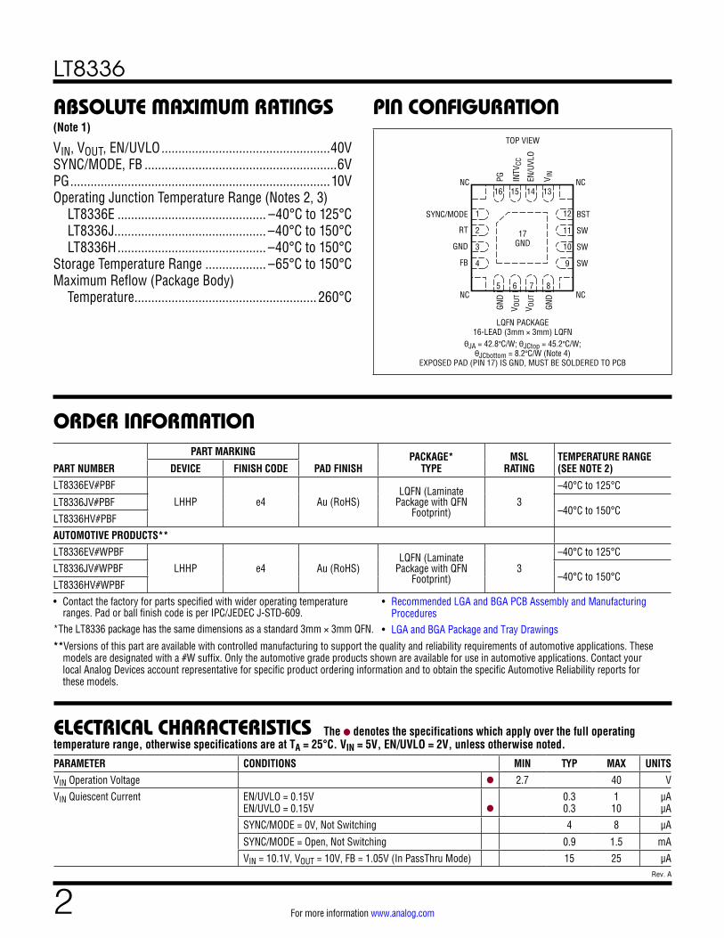
PIN CONFIGURATIONABSOLUTE MAXIMUM RATINGS
VIN, VOUT, EN/UVLO ..................................................40VSYNC/MODE, FB .........................................................6VPG .............................................................................10VOperating Junction Temperature Range (Notes 2, 3) LT8336E ............................................ –40°C to 125°C LT8336J............................................. –40°C to 150°C LT8336H ............................................ –40°C to 150°CStorage Temperature Range .................. –65°C to 150°CMaximum Reflow (Package Body)
Temperature ...................................................... 260°C
(Note 1)
16 15 14 13
5 6 7 8
TOP VIEW
LQFN PACKAGE16-LEAD (3mm × 3mm) LQFN
θJA = 42.8°C/W; θJCtop = 45.2°C/W;θJCbottom = 8.2°C/W (Note 4)
EXPOSED PAD (PIN 17) IS GND, MUST BE SOLDERED TO PCB
1SYNC/MODE
RT
GND
FB
BST
SW
SW
SW
GND
V OUT
V OUT
GND
PG INTV
CC
EN/U
VLO
V IN
12
11
10
9
2
3
4
NC
NC
NC
NC
17GND
ORDER INFORMATION
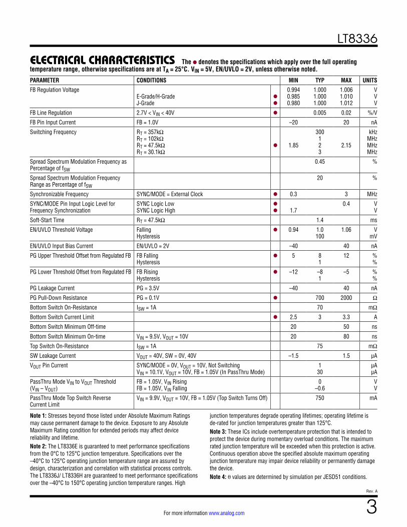
PARAMETER CONDITIONS MIN TYP MAX UNITSVIN Operation Voltage l 2.7 40 V
VIN Quiescent Current EN/UVLO = 0.15V EN/UVLO = 0.15V
l
0.3 0.3
1 10
µA µA
SYNC/MODE = 0V, Not Switching 4 8 µA
SYNC/MODE = Open, Not Switching 0.9 1.5 mA
VIN = 10.1V, VOUT = 10V, FB = 1.05V (In PassThru Mode) 15 25 µA
ELECTRICAL CHARACTERISTICS The l denotes the specifications which apply over the full operating temperature range, otherwise specifications are at TA = 25°C. VIN = 5V, EN/UVLO = 2V, unless otherwise noted.
PART NUMBER
PART MARKING
PAD FINISHPACKAGE*
TYPEMSL
RATINGTEMPERATURE RANGE (SEE NOTE 2)DEVICE FINISH CODE
LT8336EV#PBF
LHHP e4 Au (RoHS)LQFN (Laminate
Package with QFN Footprint)
3
–40°C to 125°C
LT8336JV#PBF–40°C to 150°C
LT8336HV#PBF
AUTOMOTIVE PRODUCTS**LT8336EV#WPBF
LHHP e4 Au (RoHS)LQFN (Laminate
Package with QFN Footprint)
3
–40°C to 125°C
LT8336JV#WPBF–40°C to 150°C
LT8336HV#WPBF
• Contact the factory for parts specified with wider operating temperature ranges. Pad or ball finish code is per IPC/JEDEC J-STD-609.
*The LT8336 package has the same dimensions as a standard 3mm × 3mm QFN.
• Recommended LGA and BGA PCB Assembly and Manufacturing Procedures
• LGA and BGA Package and Tray Drawings
**Versions of this part are available with controlled manufacturing to support the quality and reliability requirements of automotive applications. These models are designated with a #W suffix. Only the automotive grade products shown are available for use in automotive applications. Contact your local Analog Devices account representative for specific product ordering information and to obtain the specific Automotive Reliability reports for these models.
LT8336
3Rev. A
For more information www.analog.com
ELECTRICAL CHARACTERISTICS The l denotes the specifications which apply over the full operating temperature range, otherwise specifications are at TA = 25°C. VIN = 5V, EN/UVLO = 2V, unless otherwise noted.
Note 1: Stresses beyond those listed under Absolute Maximum Ratings may cause permanent damage to the device. Exposure to any Absolute Maximum Rating condition for extended periods may affect device reliability and lifetime. Note 2: The LT8336E is guaranteed to meet performance specifications from the 0°C to 125°C junction temperature. Specifications over the –40°C to 125°C operating junction temperature range are assured by design, characterization and correlation with statistical process controls. The LT8336J/ LT8336H are guaranteed to meet performance specifications over the –40°C to 150°C operating junction temperature ranges. High
junction temperatures degrade operating lifetimes; operating lifetime is de-rated for junction temperatures greater than 125°C.Note 3: These ICs include overtemperature protection that is intended to protect the device during momentary overload conditions. The maximum rated junction temperature will be exceeded when this protection is active. Continuous operation above the specified absolute maximum operating junction temperature may impair device reliability or permanently damage the device.Note 4: θ values are determined by simulation per JESD51 conditions.
PARAMETER CONDITIONS MIN TYP MAX UNITS
FB Regulation Voltage E-Grade/H-Grade J-Grade
l
l
0.994 0.985 0.980
1.000 1.000 1.000
1.006 1.010 1.012
V V V
FB Line Regulation 2.7V < VIN < 40V l 0.005 0.02 %/V
FB Pin Input Current FB = 1.0V –20 20 nA
Switching Frequency RT = 357kΩ RT = 102kΩ RT = 47.5kΩ RT = 30.1kΩ
l
1.85
300 1 2 3
2.15
kHz MHz MHz MHz
Spread Spectrum Modulation Frequency as Percentage of fSW
0.45 %
Spread Spectrum Modulation Frequency Range as Percentage of fSW
20 %
Synchronizable Frequency SYNC/MODE = External Clock l 0.3 3 MHz
SYNC/MODE Pin Input Logic Level for Frequency Synchronization
SYNC Logic Low SYNC Logic High
l
l
1.7
0.4 V V
Soft-Start Time RT = 47.5kΩ 1.4 ms
EN/UVLO Threshold Voltage Falling Hysteresis
l 0.94 1.0 100
1.06 V mV
EN/UVLO Input Bias Current EN/UVLO = 2V –40 40 nA
PG Upper Threshold Offset from Regulated FB FB Falling Hysteresis
l 5 8 1
12 % %
PG Lower Threshold Offset from Regulated FB FB Rising Hysteresis
l –12 –8 1
–5 % %
PG Leakage Current PG = 3.5V –40 40 nA
PG Pull-Down Resistance PG = 0.1V l 700 2000 Ω
Bottom Switch On-Resistance ISW = 1A 70 mΩ
Bottom Switch Current Limit l 2.5 3 3.3 A
Bottom Switch Minimum Off-time 20 50 ns
Bottom Switch Minimum On-time VIN = 9.5V, VOUT = 10V 20 80 ns
Top Switch On-Resistance ISW = 1A 75 mΩ
SW Leakage Current VOUT = 40V, SW = 0V, 40V –1.5 1.5 μA
VOUT Pin Current SYNC/MODE = 0V, VOUT = 10V, Not Switching VIN = 10.1V, VOUT = 10V, FB = 1.05V (In PassThru Mode)
1 30
μA μA
PassThru Mode VIN to VOUT Threshold (VIN – VOUT)
FB = 1.05V, VIN Rising FB = 1.05V, VIN Falling
0 –0.6
V V
PassThru Mode Top Switch Reverse Current Limit
VIN = 9.9V, VOUT = 10V, FB = 1.05V (Top Switch Turns Off) 750 mA

LT8336
4Rev. A
For more information www.analog.com
TYPICAL PERFORMANCE CHARACTERISTICS
Efficiency and Power Loss vs Output Current
Efficiency and Power Loss vs Output Current
Burst Mode Efficiency vs Inductor Value
Efficiency vs Output Current at Different Switching Frequencies
EN/UVLO Thresholds vs Temperature
FB Regulation Voltage vs Temperature
Oscillator Frequency vs Temperature
Oscillator Frequency with Spread Spectrum Modulation Switching Waveforms, Soft-Start
TA ≈ TJ = 25°C, unless otherwise noted.
INDUCTOR VALUE (μH)3 6 9 12 15
65
70
75
80
85
90
95
100
EFFI
CIEN
CY (%
)
8336 G03
3.3μH: COILCRAFT XFL4020-332ME4.7μH: COILCRAFT XFL4020-472ME6.8μH: COILCRAFT XEL4030-682ME10μH: COILCRAFT XAL5050-103ME15μH: COILCRAFT XAL5050-153MEFRONT PAGE CIRCUIT
ILOAD = 5mA
VIN = 16V
VIN = 8V
EN/UVLO RISING
EN/UVLO FALLING
TEMPERATURE (°C)–50 –25 0 25 50 75 100 125 150
0.99
1
1.01
1.02
1.03
1.04
1.05
1.06
1.07
1.08
1.09
EN/U
VLO
THRE
SHOL
D (V
)
8336 G05TEMPERATURE (°C)
–50 –25 0 25 50 75 100 125 1500.99
0.992
0.994
0.996
0.998
1
1.002
1.004
1.006
1.008
1.01
FB R
EGUL
ATIO
N VO
LTAG
E (V
)
3976 G06
1ms/DIV 8336 G09
IL1A/DIV
VOUT10V/DIV
EN/UVLO2V/DIV
VIN = 12VFRONT PAGE CIRCUIT
24V
OUTPUT CURRENT (mA)0.1 1 10 100 1k 10k
0
10
20
30
40
50
60
70
80
90
100
1
10
100
1k
10k
EFFI
CIEN
CY (%
)
POWER LOSS (m
W)
8336 G01
VIN = 16VVIN = 8V
FRONT PAGE CIRCUITBurst Mode OPERATION
VIN = 12VFRONT PAGE CIRCUIT
OUTPUT CURRENT (mA)1 10 100 1k
0
10
20
30
40
50
60
70
80
90
100
0.1
1
10
100
1k
10k
EFFI
CIEN
CY (%
)
POWER LOSS (m
W)
8336 G02
BURST EFFICIENCY
BURST LOSS
PULSE–SKIPPINGEFFICIENCY
PULSE–SKIPPINGLOSS
LOAD CURRENT (mA)0.1 1 10 100 1000
0
10
20
30
40
50
60
70
80
90
100
EFFI
CIEN
CY (%
)
8336 G04
300kHz, L = 47μH1MHz, L = 15μH2MHz, L = 6.8μH3MHz, L = 4.7μH
VIN = 12V
FRONT PAGE CIRCUITBurst Mode OPERATION
TEMPERATURE (°C)–50 –25 0 25 50 75 100 125 150
1.9
1.92
1.94
1.96
1.98
2
2.02
2.04
2.06
2.08
2.1
OSCI
LLAT
OR F
REQU
ENCY
(MHz
)
8336 G07
RT = 47.5kΩSYNC/MODE = OPEN
TIME (μs)
OSCI
LLAT
OR F
REQU
ENCY
(MHz
)
8336 G08
0 50 100 150 200 250 3001.9
2.1
2.0
2.2
2.3
2.4
2.5RT = 47.5kΩSYNC/MODE = INTVCC

LT8336
5Rev. A
For more information www.analog.com
TYPICAL PERFORMANCE CHARACTERISTICS TA ≈ TJ = 25°C, unless otherwise noted.
Switching Waveforms, Soft-Start at Different VIN Voltages
Bottom Switch Current Limit vs Temperature
Max Programmable Switching Frequency vs Input Voltage
Switching Waveforms, Current Limit at 15% Duty Cycle
Switching Waveforms, Current Limit at 85% Duty Cycle
Power Switch Voltage Drop vs Switch Current
Power Switch Voltage Drop vs Temperature
Switching Waveforms, Load Step in Pulse-Skipping Mode Operation
Switching Waveforms, Load Step in Burst Mode Operation
TEMPERATURE (°C)–50 –25 0 25 50 75 100 125 150
2.5
2.6
2.7
2.8
2.9
3.0
3.1
3.2
CURR
ENT
LIM
IT (A
)
Temperature
8336 G11
VIN (V)2.70 2.75 2.80 2.85 2.90 2.95 3.000
0.5
1.0
1.5
2.0
2.5
3.0
3.5
MAX
SW
ITCH
ING
FREQ
UENC
Y (M
Hz)
8336 G12
SWITCH CURRENT (A)0 0.5 1 1.5 2 2.5 3
0
50
100
150
200
250
300
SWIT
CH D
ROP
(mV)
8336 G15
TOP SWITCH
BOTTOM SWITCH
TEMPERATURE (°C)–50 –25 0 25 50 75 100 125 150
0
20
40
60
80
100
120
140
160
SWIT
CH D
ROM
(mV)
8336 G16
TOP SWITCH
BOTTOM SWITCH
SWITCH CURRENT = 1A
500ns/DIV 8336 G13
IL1A/DIV
0A
VSW10V/DIV
VIN = 4.15VFRONT PAGE CIRCUIT
500ns/DIV 8336 G14
IL1A/DIV
0A
VSW10V/DIV
VIN = 21.5VFRONT PAGE CIRCUIT
200μs/DIV
0.5A
8336 G17
IL1A/DIV
IOUT0.5A/DIV
VOUT0.5V/DIV
(AC)
FRONT PAGE CIRCUIT
0A
200μs/DIV 8336 G18
IL1A/DIV
IOUT0.5A/DIV
VOUT0.5V/DIV
(AC)
FRONT PAGE CIRCUIT
0A
0.5A
500μs/DIV 8336 G10
VOUT10V/DIV
0V
EN/UVLO2V/DIV
FRONT PAGE CIRCUIT
VOUT AT VIN = 16VVOUT AT VIN = 12VVOUT AT VIN = 8V

LT8336
6Rev. A
For more information www.analog.com
TYPICAL PERFORMANCE CHARACTERISTICS
Minimum On/Off Times vs Temperature
Switching Waveforms, Full Frequency PWM Operation
Switching Waveforms, Continuous Burst Mode Operation
Switching Waveforms, Discontinuous Burst Mode Operation
Switching Waveforms, Light Load Low IQ Burst Mode Operation
Switching Waveforms, Discontinuous Pulse-Skipping Mode
Waveforms, PassThru Mode Operation
Waveforms, Reverse Current Protection in PassThru Mode
Switching Waveforms, Frequency Foldback when VIN is close to VOUT
TA ≈ TJ = 25°C, unless otherwise noted.
TEMPERATURE (°C)–50 –25 0 25 50 75 100 125 150
0
10
20
30
40
50
60
70
MIN
ON/
OFF
TIM
ES (n
s)
3976 G19
MIN ON TIME
MIN OFF TIME
VOUT = 30V
2μs/DIV 8336 G20
IL0.5A/DIV
0A
VSW10V/DIV
VIN = 3VILOAD = 220mASYNC/MODE = 0V BACK PAGE CIRCUIT
2μs/DIV 8336 G21
IL0.5A/DIV
0A
VSW10V/DIV
VIN = 3VILOAD = 110mASYNC/MODE = 0V BACK PAGE CIRCUIT
2μs/DIV 8336 G22
IL0.5A/DIV
0A
VSW10V/DIV
VIN = 3VILOAD = 50mASYNC/MODE = 0V BACK PAGE CIRCUIT
10ms/DIV 8336 G23
IL0.5A/DIV
0A
VSW10V/DIV
VIN = 3VILOAD = 0mASYNC/MODE = 0V BACK PAGE CIRCUIT
500ns/DIV 8336 G24
IL0.1A/DIV
0A
VSW10V/DIV
VIN = 3VILOAD = 10mASYNC/MODE = OPEN BACK PAGE CIRCUIT
2μs/DIV 8336 G25
VOUT, VIN1V/DIV
IL0.5A/DIV
VSW20V/DIV
ILOAD = 0.5AVIN = 10.45VSYNC/MODE = 0V BACK PAGE CIRCUIT
VIN
VOUT
0.5A
50μs/DIV 8336 G26
VOUT, VIN1V/DIV
IL0.5A/DIV
VSW20V/DIV
SYNC/MODE = 0V BACK PAGE CIRCUIT
VOUT
VIN
–750mA
10.6V
100mA
2μs/DIV 8336 G27
VOUT, VIN1V/DIV
IL0.5A/DIV
VSW20V/DIV
ILOAD = 0.5AVOUT = 10VSYNC/MODE = 0V BACK PAGE CIRCUIT
VOUT
VIN
0.5A

LT8336
7Rev. A
For more information www.analog.com
Conducted EMI Performance (CISPR25 Class 5 Peak)
TYPICAL PERFORMANCE CHARACTERISTICS TA ≈ TJ = 25°C, unless otherwise noted.
Radiated EMI Performance (CISPR25 Class 5 Peak)
FREQUENCY (MHz)0 3 6 9 12 15 18 21 24 27 30
–20
–10
0
10
20
30
40
50
60
70
80
AMPL
ITUD
E (d
BµV)
8336 G28
CLASS 5 PEAK LIMITLT8336 PEAK EMI
PAGE 18 CIRCUIT, 12V INPUT TO 24V OUTPUT AT 600mA, SSFM = ON, fSW = 2MHz TO 2.4MHz
FREQUENCY (MHz)0 3 6 9 12 15 18 21 24 27 30
–20
–10
0
10
20
30
40
50
60
70
80
AMPL
ITUD
E (d
BµV)
8336 G29
CLASS 5 AVERAGE LIMITLT8336 AVERAGE EMI
PAGE 18 CIRCUIT, 12V INPUT TO 24V OUTPUT AT 600mA, SSFM = ON, fSW = 2MHz TO 2.4MHz
FREQUENCY (MHz)0 100 200 300 400 500 600 700 800 900 1000
–20
–10
0
10
20
30
40
50
60
AMPL
ITUD
E (d
BµV/
m)
8336 G30
CLASS 5 PEAK LIMITLT8336 PEAK EMI
PAGE 18 CIRCUIT, 12V INPUT TO 24V OUTPUT AT 600mA, SSFM = ON, fSW = 2MHz TO 2.4MHz
FREQUENCY (MHz)0 100 200 300 400 500 600 700 800 900 1000
–20
–10
0
10
20
30
40
50
60
AMPL
ITUD
E (d
BµV/
m)
8336 G31
CLASS 5 AVERAGE LIMITLT8336 AVERAGE EMI
PAGE 18 CIRCUIT, 12V INPUT TO 24V OUTPUT AT 600mA, SSFM = ON, fSW = 2MHz TO 2.4MHz
Conducted EMI Performance (CISPR25 Class 5 Average)
Radiated EMI Performance (CISPR25 Class 5 Average)

LT8336
8Rev. A
For more information www.analog.com
PIN FUNCTIONSSYNC/MODE (Pin 1): External Synchronization Input and Mode Selection Pin. This pin allows five selectable modes for optimization of performance:
SYNC/MODE PIN INPUT CAPABLE MODE(S) OF OPERATION
(1) GND or <0.1V Burst
(2) 50k Resistor to GND Burst/SSFM
(3) Float (Pin Open) Pulse-Skipping
(4) INTVCC or > (INTVCC – 0.2V) Pulse-Skipping/SSFM
(5) External Clock Pulse-Skipping/Sync
where the selectable modes of operation are:
Burst = low IQ, (low output ripple operation at light loads) Pulse-Skipping = skipped pulse(s) at light load (aligned clock) SSFM = spread spectrum frequency modulation for low EMI Sync = switching frequency synchronized to external clock
The LT8336 automatically selects pulse-skipping mode with no spread-spectrum frequency modulation during start-up, and The SYNC/MODE pin input configurations (1) through (4) are ignored.
The LT8336 automatically select low IQ operation in the PassThru mode operation, and all the SYNC/MODE pin input configurations are ignored.
RT (Pin 2): Switching Frequency Adjustment Pin. The LT8336 switching frequency is programmed by connect-ing a resistor of the appropriate value from the RT pin to GND at Pin 3. See the Applications Information section for more detail. Do not leave the RT pin open.
GND (Pins 3, 5, 8, Exposed Pad Pin 17): Ground. The exposed pad should be soldered to the PCB ground plane for good thermal and electrical performance. See the Applications Information section for sample layout.
FB (Pin 4): Feedback Input Pin. This pin receives the feed-back voltage from the external resistor divider between VOUT and Pin 3 GND. FB pin is one input to the error amplifier of the output voltage control loop. See the Applications Information section for sample layout.
VOUT (Pins 6, 7): Output Pins. Connect one 1µF capaci-tor between VOUT at Pin 6 and GND at Pin 5 only, and a matching 1µF capacitor between VOUT at Pin 7 and GND
at Pin 8 only. These two capacitors complete the Silent Switcher configuration and must be placed as close to the IC as possible to achieve lowest EMI. Additional bulk capacitors of 2.2µF or more should be placed close to the IC with the positive terminals connected to VOUT, and negative terminals connected to ground plane. See the Applications Information section for a sample layout.
SW (Pins 9, 10, 11): The SW pins are the outputs of the internal power switches. Tie these pins together and connect them to the inductor and one side of the boost capacitor CBST.
BST (Pin 12): Top Switch Gate Driver Supply Pin. Place a 0.1µF capacitor (CBST) between the BST and SW pins and close to the IC.
VIN (Pin 13): Input Supply Pin. This pin must be con-nected to the input of the power stage (the inductor’s input terminal).
EN/UVLO (Pin 14): Enable and Input Undervoltage Lockout Pin. The IC is shut down when this pin is below 1V (typical). The IC draws a low VIN current of 0.3μA (typical) when this pin is below 0.15V. The IC is enabled when this pin is above 1.0V (typical). A resistor divider from VIN to GND can be used to program a VIN threshold below which the IC is shut down. See the Applications Information section for further details. Tie EN/UVLO to VIN if the shutdown feature is not used.
INTVCC (Pin 15): Internal 3.5V Regulator Bypass Pin. This pin provides supply for internal drivers and control circuits. The bypass capacitor for INTVCC should be con-nected to the ground plane. Do not load the INTVCC pin with external circuitry. This pin must be bypassed with a 1µF or larger low ESR ceramic capacitor placed close to the pin.
PG (Pins 16): Power Good Indicator. Open-drain logic output that is pulled to ground when the output voltage is greater than ±8% outside the regulated voltage. PG is also pulled to ground when EN/UVLO is below 1V, INTVCC has fallen too low, or the IC enters thermal shutdown.

LT8336
9Rev. A
For more information www.analog.com
BLOCK DIAGRAM
RT
RT
OSC
SYNC/MODE12
SS
–
+
– +
VC
FB
SYNC/MODE
OSC
VC
SHDN
4
1V
SS EA
A1
M1
INTVCC
M2
FB
R1
R2
SHDN
VOUT(6, 7)
COUT1,2 COUT3
C1
VOUT
INTVCC
CVCC
1215
CIN
VIN
13VIN
14
R4 R3
– +
A2
1V
GND(3, 5, 8, 17)
8336 BD
FB
BST
CBST
SW (9, 10, 11)
ILL
EN/UVLO
UVLO
OSCILLATOR
RAMPGENERATOR
VIN_HIGH
I_ZERO
VOUT_OVLO
BURST MODE DETECT
SWITCHINGLOGICAND
CHARGEPUMP
G1
G2
3.5V REGAND UVLO
1V REF
TJ > 170°C
+
±8%
PG16
FB
INTVCC
R5
SHDN A6
+–
VIN
40V
VIN_HIGH
I_ZERO
VOUT_OVLO
A3
+–
A4
+–
A5
LT8336
10Rev. A
For more information www.analog.com
OPERATIONThe LT8336 uses a fixed frequency, current mode con-trol scheme to provide excellent line and load regulation. Referring to the Block Diagram, the Switching Logic and Charge Pump block turns on the power switch M1 through driver G1 at the start of each oscillator cycle. During the M1 switch on-phase, the inductor current IL flows through M1. A current proportional to the M1 switch current is added to a stabilizing slope compensation ramp and the resulting sum is fed into the positive terminal of the PWM comparator A1. The voltage at the negative input of A1, labeled “VC”, is set by the error amplifier EA and is an amplified version of the difference between the feedback voltage FB and the reference voltage. During the M1 on-phase, IL increases. When the signal at the positive input of A1 exceeds VC, A1 sends out a signal to the Switching Logic and Charge Pump block to turn off M1. When M1 turns off, the synchronous power switch M2 turns on until the next clock cycle begins or induc-tor current IL falls to zero. During the M1 off-phase, IL decreases. Through this repetitive action, the EA sets the correct IL peak current level to keep the output in reg-ulation. VIN and VOUT are constantly monitored by the LT8336. When VIN rises above VOUT (causing A3’s output high) and at the same time VOUT is higher than its reg-ulation voltage programmed by the FB resistor network, the LT8336 enters PassThru operation, where M2 is kept on continuously and M1 is kept off continuously, and the VOUT is essentially shorted to VIN by the inductor and M2. See Applications Information section for further details.
LT8336 features Silent Switcher architecture to minimize EMI emissions while delivering high efficiency. The Silent Switcher EMI cancellation loops are completed by placing
one 1µF capacitor between VOUT at pin 6 and GND at pin 5 and a matching 1µF capacitor between VOUT at pin 7 and GND at pin 8 (see Applications Information section for further details).
The EN/UVLO pin controls whether the LT8336 is enabled or is in shutdown state. A 1.0V reference and a compara-tor A2 with 100mV hysteresis (Block Diagram) allow the user to accurately program the supply voltage at which the IC turns on and off. See the Applications Information section for further details.
The LT8336 features a variety of operation modes which can be selected by SYNC/MODE pin to optimize the con-verter performance based on the application requirements. The low ripple Burst Mode operation can be selected to optimize the efficiency at light loads. The spread spec-trum frequency modulation function can be selected to minimize the EMI emissions.
Pulling SYNC/MODE pin to ground selects Burst Mode operation. Connecting this SYNC/MODE to ground through a 50k resistor selects Burst Mode operation with spread spectrum frequency modulation. Floating SYNC/MODE pin selects pulse-skipping operation. Connecting SYNC/MODE pin to INTVCC selects pulse-skipping oper-ation with spread spectrum frequency modulation. If a clock is applied to the SYNC/MODE pin, the LT8336 syn-chronizes to an external clock frequency and operates in pulse-skipping mode. See the Applications Information section for further details.

LT8336
11Rev. A
For more information www.analog.com
APPLICATIONS INFORMATIONvalue. In this condition, the LT8336 maintains the output regulation voltage by reducing the switching frequency instead of reducing the inductor peak current. In light load Burst Mode operation the LT8336 delivers single pulses of current to the output capacitor followed by sleep periods during which the output power is supplied by the output capacitor. This low ripple Burst Mode operation minimizes the input quiescent current and minimizes output voltage ripple. While in sleep mode the LT8336 VIN pin draws 4µA.
As the output load decreases, the frequency of single current pulses decreases and the percentage of time the LT8336 is in sleep mode increases, resulting in much higher light load efficiency than for typical converters. By maximizing the time between pulses, the converter VIN pin quiescent current approaches 4μA for a typical application when there is no output load. To optimize the quiescent current performance at light loads, the current in the feedback resistor divider should be minimized as it appears to the output as load current.
In order to achieve higher light load efficiency, more energy should be delivered to the output during the single small pulses in Burst Mode operation such that the LT8336 can stay in sleep mode longer between each pulse. This can be achieved by using a larger value inductor. For example, while a smaller inductor value would typically be used for a high switching frequency application, if high light load efficiency is desired, a larger inductor value should be chosen. See the Burst Mode Efficiency vs Inductor Value curve in the Typical Performance Characteristics section for more information.
While in Burst Mode operation the bottom switch peak current is approximately 700mA as shown in the Switching Waveforms in Burst Mode operation curve in the Typical Performance Characteristics section. This behavior results in larger output voltage ripple compared to that in pulse-skipping mode operation which has lower bottom switch peak current. However, the output voltage ripple can be reduced proportionally by increasing the output capacitance. When adjusting output capacitance, a careful evaluation of system stability should be made to ensure adequate design margin. As the load ramps upward from zero, the switching frequency keeps increas-ing until reaching the switching frequency programmed by the resistor at the RT pin. The output load at which the
Programming VIN Turn-On and Turn-Off Thresholds with the EN/UVLO Pin
The falling threshold voltage and rising hysteresis voltage of the VIN pin can be calculated by Equation 1.
VVIN,FALLING = 1.0V • (R3 + R4)
R4
VVIN,RISING = 100mV • (R3 + R4)R4
+VVIN,FALLING
(1)
When in Burst Mode operation with light load currents, the current through the resistor network R3 and R4 can easily be greater than the supply current consumed by the LT8336. Therefore, large resistors can be used for R3 and R4 to minimize their effect on efficiency at light loads.
EN/UVLO pin can be tied to VIN if the shutdown feature is not used, or alternatively, the pin may be tied to a logic level if shutdown control is required. The IC draws a low VIN quiescent current of 0.3µA (typical) When EN/UVLO is below 0.15V.
INTVCC Regulator
An internal low dropout (LDO) regulator produces the 3.5V supply from VIN that powers the drivers and the internal bias circuitry. The INTVCC pin must be bypassed to ground with a minimum of 1μF ceramic capacitor. Good bypassing is necessary to supply the high transient currents required by the power MOSFET gate drivers. Applications with high VIN voltage and high switching frequency increase die tem-perature because of the higher power dissipation across the LDO. When VIN is lower than 2.9V, the maximum programmable switching frequency is lower due to the voltage drop across the LDO. See the Max Programmable Switching Frequency vs Input Voltage curve in the Typical Performance Characteristics section for more information. Do not connect an external load to the INTVCC pin.
Light Load Current Operation—Burst Mode Operation or Pulse-Skipping
To enhance the efficiency at light loads, the LT8336 fea-tures operate in low ripple Burst Mode operation. When the LT8336 is enabled for Burst Mode operation, the mini-mum peak inductor current is set to approximately 700mA even though the VC node (Block Diagram) indicates a lower

LT8336
12Rev. A
For more information www.analog.com
LT8336 reaches the programmed frequency varies based on input voltage, output voltage, and inductor choice.
Pulse-skipping mode operation offers two major dif-ferences from Burst Mode operation. First, the internal clock stays awake at all times and all switching cycles are aligned to the clock. In this mode the internal circuitry is awake at all times, increasing quiescent current to hun-dred μA compared to the 4μA of VIN pin quiescent cur-rent in Burst Mode operation. Second, as the load ramps upward from zero, the switching frequency programmed by the resistor at the RT pin is reached at a lower output load than in Burst Mode operation, therefore, pulse-skip-ping mode operation exhibits lower output ripple as well as lower audio noise and RF interference.
Switching Frequency and Synchronization
The choice of switching frequency is a trade-off between efficiency and component size. Low frequency operation improves efficiency by reducing the power switches’ switching losses and gate drive current. However, lower frequency operation requires a physically larger inductor. The LT8336 uses a constant-frequency architecture that can be programmed over a 300kHz to 3MHz range with a single external resistor from the RT pin to ground, as shown in Block Diagram. A table for selecting the value of RT for a given switching frequency is shown in Table 1. Figure 1 shows the RT Value vs Switching Frequency curve.
Table 1. SW Frequency (fSW) vs RT ValuefSW (MHz) RT (kΩ) fSW (MHz) RT (kΩ)
0.3 357 1.7 57.60.4 267 1.8 53.60.5 210 1.9 51.10.6 174 2.0* 47.50.7 147 2.1 45.20.8 127 2.2 43.20.9 113 2.3 40.21.0 102 2.4 39.21.1 90.9 2.5 37.41.2 84.5 2.6 35.71.3 76.8 2.7 34.01.4 71.5 2.8 32.41.5 64.9 2.9 30.91.6 61.9 3.0 30.1
*Programming 2MHz will ensure fSW stays above 1.85MHz (out of AM band).
The operating frequency of the LT8336 can be synchro-nized to an external clock source with 100ns minimum pulse width. By providing a digital clock signal to the SYNC/MODE pin, the LT8336 operates at the SYNC pulse frequency and automatically enters pulse-skipping mode operation at light load. If this feature is used, an RT resis-tor should be chosen to program a switching frequency as close as possible to the SYNC pulse frequency.
Spread Spectrum Frequency Modulation
The LT8336 features spread spectrum frequency mod-ulation to further reduce EMI emissions. The user can select spread spectrum frequency modulation with Burst Mode operation by connecting the SYNC/MODE pin to ground through a 50k resistor, or spread spectrum fre-quency modulation with pulse-skipping operation by con-necting the SYNC/MODE pin to INTVCC. When spectrum frequency modulation is selected, a stepped triangular frequency modulation is used to vary the internal oscil-lator frequency between the value programmed by the RT resistor to approximately 20% higher than that value. The modulation frequency is approximately 0.45% of the switching frequency. For example, when the LT8336 is programmed to 2MHz, and spread spectrum frequency modulation is selected, the oscillator frequency varies from 2MHz to 2.4MHz at a 9kHz rate (see Oscillator Frequency with Spread Spectrum Modulation curve in the Typical Performance Characteristics section). When operating at light load, the spread spectrum frequency modulation is more effective in pulse-skipping mode than
APPLICATIONS INFORMATION
Figure 1. RT Value vs Switching Frequency
SWITCHING FREQUENCY (kHz)0 500 1000 1500 2000 2500 3000
10k
100k
1M
R T(Ω
)
8336 F01

LT8336
13Rev. A
For more information www.analog.com
in Burst Mode operation, due to the fact that pulse-skip-ping operation maintains the programmed switching fre-quency down to a much lower load current as compared to Burst Mode operation.
VIN to VOUT PassThru Mode Operation
In the boost pre-regulator applications for automotive stop-start and cold crank, VIN is normally above the reg-ulated VOUT voltage. In this condition, LT8336 enters PassThru operation. LT8336 is designed to have an accurate, well controlled PassThru operation with low quiescent current consumption. If VIN transiently falls below the VOUT regulation setpoint, the boost converter commences switching to maintain the output voltage in regulation.
As shown in Block Diagram, VIN is compared with VOUT using the comparator A3 with 0.6V hysteresis. When VIN rises above VOUT (causing A3’s output high), and at the same time VOUT is higher than its regulation voltage pro-grammed by the FB resistor network, the LT8336 boost converter enters PassThru operation, where the synchro-nous power switch M2 is kept on continuously and the power switch M1 is kept off continuously. The voltage across the boost capacitor (CBST), VBST_SW, is constantly monitored. When VBST_SW drops below 3.2V, an inter-nal charge pump is turned on to charge VBST_SW up to 3.6V, and then turned off. In PassThru mode the VOUT is essentially shorted to VIN by the inductor and M2, and VIN pin quiescent current is limited to 15µA (typ) regardless of the SYNC/MODE pin’s configuration. VOUT pin draws 30µA (typ). A typical waveforms drawing is shown in the Typical Performance Characteristics section.
Several conditions cause the LT8336 to exit from the PassThru mode operation. First, when VOUT drops below its regulation voltage programmed by the FB resistor net-work, LT8336 exits from PassThru mode operation and normal boost switching operation resumes to maintain the regulated VOUT voltage. Second, when VOUT is still higher than its regulation voltage but VIN drops below VOUT by the comparator A3’s hysteresis of 0.6V (typ) or more to cause A3’s output low, M2 is turned off to prevent the reverse current from VOUT to VIN from ramping up. LT8336 is back to the PassThru mode when A3’s output
is high again. Third, when VOUT is still higher than its regulation voltage but M2’s reverse current (flowing from its drain to source) rises above 750mA (typ), M2 is turned off to prevent the reverse current from VOUT to VIN from ramping up. LT8336 re-enters the PassThru mode when A3’s output is high again. Waveforms for typical reverse current protection are shown in the Typical Performance Characteristics section.
To ensure the PassThru mode operation works properly, the LT8336’s VIN pin must be connect to the input of the power stage (the input terminal of inductor as shown in Block Diagram).
FB Resistor Network and the Quiescent Current at No-Load
The output voltage is programmed with a resistor divider between the output and the FB pin. Choose the resistor values according to Equation 2.
R1 = R2 •
VOUT1V
– 1⎛⎝⎜
⎞⎠⎟
(2)
Reference designators refer to Block Diagram. The 1% resistors are recommended to maintain output voltage accuracy.
If low input quiescent current and good light-load effi-ciency are desired, use large resistor values for the FB resistor divider. The current flowing in the divider acts as a load current, and will increase the no-load input current to the converter.
When VIN < VOUT, the converter Burst Mode quiescent current at no-load can be estimated using Equation 3.
I ≈
VOUT
R1 + R24µA 1µA+ +
VOUTVIN
1.25••Q⎛
⎝⎜
⎛
⎝⎜
⎞
⎠⎟
⎞
⎠⎟
(3)
where 4μA is the VIN pin quiescent current of the LT8336, and the second term is the current drawn by the feedback divider and VOUT pin (1μA) reflected to the input of the boost operating.
For a 12V input, 24V output boost converter with R1 = 1M and R2 = 43.2k, it can be calculated that the converter draws approximately 64μA from the 12V supply at
APPLICATIONS INFORMATION

LT8336
14Rev. A
For more information www.analog.com
no-load. Note that this equation implies that the no-load current is a function of VIN.
When VIN is higher than the regulated VOUT voltage, LT8336 enters PassThru operation and VOUT is essen-tially shorted to VIN by the inductor and M2. The con-verter quiescent current at no-load can be estimated using Equation 4.
I ≈
VIN
R1 + R245µA +Q
(4)
where 45μA is the sum of the VIN pin and VOUT pin qui-escent current of the LT8336, and the second term is the current drawn by the feedback divider.
For a 25V VIN with R1 = 1M and R2 = 43.2k, it can be calculated that the converter draws approximately 70μA from the 25V supply at no-load.
When using large FB resistors, a 4.7pF to 22pF phase-lead capacitor should be connected from VOUT to FB, and a careful evaluation of system stability should be made to ensure adequate design margin.
Overvoltage Lockout
The VOUT pin voltage is constantly monitored by the LT8336. An overvoltage condition occurs when VOUT pin voltage exceeds approximately 40V. Switching is stopped at such condition. Normal switching is resumed when the VOUT pin voltage drops back to 40V or lower.
Switching Frequency Foldback when VIN Approaches VOUT
In some applications, VIN may rise to a voltage very close to VOUT. In this condition the switching regulator must operate at a very low duty cycles to keep VOUT in reg-ulation. However, the minimum on-time limitation may prevent the switcher from attaining a sufficiently low duty cycle at the programmed switching frequency. As a result a typical boost converter may experience a large output ripple under these conditions. The LT8336 addresses this issue by adopting a switching frequency foldback function to smoothly decrease the switching frequency when its minimum on-time starts to limit the switcher from attain-ing a sufficiently low duty cycle. The typical switching
waveforms in these VIN approaching VOUT conditions are shown in the Typical Performance Characteristics section.
Start-Up
To limit the peak switch current and VOUT overshoot during start-up, the LT8336 contains internal circuitry to provide soft-start operation (refer to the error amplifier EA in Block Diagram). During start-up, the internal soft-start circuity slowly ramps the internal SS signal from zero to 1V. When the SS voltage falls between the FB initial volt-age and 1V, the LT8336 regulates the FB pin voltage to the SS voltage instead of 1V. In this way the output capacitor is charged gradually towards its final value while limiting the start-up peak switch currents.
Referring to Figure 2, the start-up time TSTART_UP is the time period from EN/UVLO transitioning high to PG transitioning high, indicating VOUT has reached approxi-mately 90% of its regulation voltage programmed by FB resistor network. When VIN > 3.6V, TSTART_UP is approx-imately given by Equation 5.
TSTART _UP = 0.25ms+ 2100
fSW (5)
When VIN < 3.6V, TSTART_UP is approximately given by Equation 6.
TSTART _UP = 0.25ms+ 3.5V
VIN − 0.1V• 2100
fSW (6)
APPLICATIONS INFORMATION
Figure 2. Typical Start-Up Waveforms
1ms/DIV 8336 F02
IL1A/DIV
VOUT10V/DIV
EN/UVLO2V/DIV
VIN = 12VFRONT PAGE CIRCUIT
tMODE_DELAY
tSTART_UP
24V
The LT8336 selects pulse-skipping mode with no spread spectrum frequency modulation during start-up, and the SYNC/MODE pin configuration is ignored. The LT8336

LT8336
15Rev. A
For more information www.analog.com
Figure 3. A Simplified LT8336 Power Stage with a Diode Added Between VIN and VOUT
reads SYNC/MODE pin configuration after the start-up delay given by Equation 7.
TMODE_DELAY = 0.22ms+ 4096
fSW (7)
If the LT8336 boost converter is plugged into a live sup-ply, the VOUT could ring to twice the voltage of VIN, due to the resonant circuit composed by L, COUT1-3, and the body diode of M2 (refer to Block Diagram). If such over-shoot exceeds the VOUT rating, it must be limited to protect the load and the converter. For these situations, a small Schottky diode or silicon diode can be connected between VIN and VOUT to deactivate the resonant circuit and limit the VOUT over-shoot as shown in Figure 3. With the diode connected, the LT8336 boost is also more robust against output fault conditions such as output short circuit or overload, due to the fact that the diode diverts a great amount of output current from the LT8336. The diode can be rated for about one half to one fifth of the full load current since it only conducts current during start-up or output fault conditions.
The inductor ripple current ∆ISW has a direct effect on the choice of the inductor value, the converter’s maximum output current capability, and the light load efficiency in Burst Mode operation. Choosing smaller values of ∆ISW increases output current capability and light load effi-ciency in Burst Mode operation, but require large induc-tance values and reduce the current loop gain. Accepting larger values of ∆ISW provides fast transient response and allows the use of low inductance values, but results in higher input current ripple, greater core losses, lower light load efficiency in Burst Mode operation, and lower output current capability. Large values of ∆ISW at high duty cycle operation may result in sub-harmonic oscillation. ∆ISW = 0.3A to 0.6A generally provides a good starting value for many applications, and careful evaluation of system sta-bility should be made to ensure adequate design margin.
Given an operating input voltage range, and having cho-sen the operating frequency and ripple current in the inductor, the inductor value of the boost converter can be determined using Equation 9.
L =
VIN(MIN)
∆ISW • fSW•DMAX
(9)
The LT8336 limits the peak switch current in order to pro-tect the switches and the system from overload faults. The bottom switch current limit is controlled to 3A (typical) regardless of the duty cycle. The peak inductor current is equal to the LT8336 bottom switch current limit. The user should choose an inductor with sufficient saturation and RMS current ratings to handle the inductor’s peak current.
Input Capacitor Selection
The input ripple current in a boost converter is relatively low (compared with the output ripple current), because this current is continuous. The voltage rating of the input capacitor, CIN, should comfortably exceed the maximum input voltage. Although ceramic capacitors can be rela-tively tolerant of overvoltage conditions, aluminum elec-trolytic capacitors are not. Be sure to characterize the input voltage for any possible overvoltage transients that could apply excess stress to the input capacitors.
APPLICATIONS INFORMATION
VIN
VIN
SW
GND
VOUT
VOUT
CIN
L
COUT1,2
COUT3
D
LT8336
8336 F03
Inductor Selection
When operating in continuous conduction mode (CCM), the duty cycle can be calculated based on the output volt-age (VOUT) and the input voltage (VIN). The maximum duty cycle (DMAX) occurs when the converter has the minimum input voltage given by Equation 8.
DMAX =
VOUT – VIN(MIN)
VOUT (8)
Discontinuous conduction mode (DCM) provides higher conversion ratios at a given frequency at the cost of reduced efficiencies and higher switching currents.

LT8336
16Rev. A
For more information www.analog.com
The value of CIN is a function of the source impedance, and in general, the higher the source impedance, the higher the required input capacitance.
The RMS CIN ripple current can be estimated by Equation 10.
IRMS(CIN) = 0.3 • ∆IL (10)
Output Capacitor Selection
The output capacitor has two essential functions. First, it filters the LT8336’s discontinuous top switch current to produce the DC output. In this role, it determines the out-put ripple, thus low impedance at the switching frequency is important. The second function is to store energy in order to satisfy transient loads and stabilize the LT8336’s control loop. The X5R or X7R type ceramic capacitors have very low equivalent series resistance (ESR), which provides low output ripple and good transient response. Transient performance can be improved with higher out-put capacitance and the addition of a feedforward capac-itor placed between VOUT and FB. When a feedforward capacitor is used or output capacitance is adjusted, a careful evaluation of system stability should be made to ensure adequate design margin. Increasing the output capacitance will also decrease the output voltage ripple. Lower value of output capacitance can be used to save space and cost, but transient performance will suffer and loop instability may result.
Besides the bulk output capacitors, two small output ceramic capacitors, 1µF each, should be placed as close as possible to the IC to complete the Silent Switcher can-cellation loops.
See the Board Layout section for more detail. XR7 or X5R capacitors are recommended for best performance across temperature and output voltage variations. Note that larger output capacitance is required when a lower switching frequency is used. If there is significant induc-tance to the load due to long wires or cables, additional bulk capacitance may be necessary. This can be provided
APPLICATIONS INFORMATION
Figure 4. A Recommended PCB Layout for the LT8336
RT
R4
CVCC
COUT3
VIN
R3
R5
8336 F04
COUT2
COUT1
CBST
L
CIN1
1
R1
R2
C1
GROUND VIA PG SIGNAL VIA
VOUT
GND GND
with an electrolytic capacitor. When choosing a capacitor, special attention should be given to capacitor's data sheet to calculate the effective capacitance under the relevant operating conditions of voltage bias and temperature. A physically larger capacitor, or one with a higher voltage rating, may be required. For good starting values, refer to the Typical Applications section.
Board Layout
The LT8336 is specifically designed to minimize EMI emissions and also to maximize efficiency when switch-ing at high frequencies. Figure 4 shows a recommended

LT8336
17Rev. A
For more information www.analog.com
APPLICATIONS INFORMATIONPCB layout. For more detail and PCB design files refer to the demo board guide for the LT8336.
For optimal performance the LT8336 requires the use of multiple VOUT bypass capacitors. It is recommended to connect one 1µF capacitor between VOUT at Pin 6 and GND at Pin 5 only, and a matching 1µF capacitor between VOUT at Pin 7 and GND at Pin 8 only to complete the Silent Switcher EMI cancellation loops. These two capacitors must be placed as close as possible to the IC, and the loops formed by these two capacitors should be sym-metrical and as small as possible to achieve an optimized EMI cancellation performance. Capacitors with small case size, such as 0402 or 0603, are optimal due to the low parasitic inductance. Additional bulk capacitors of 2.2µF or more should be placed close to the IC with the posi-tive terminals connected to VOUT, and negative terminals connected to ground plane. The bypass capacitors for VIN and INTVCC pins should also be connected to the ground plane.
The output capacitors, along with the inductor and input capacitors, should be placed on the same side of the circuit board, and their connections should be made on that layer. Place a local, unbroken power ground plane under the application circuit on the layer closest to the surface layer. The SW and BST nodes should be as small as possible.
Keep the FB and RT nodes small so that the ground traces will shield them from the noise generated by the SW and BST nodes. It is recommended to use the GND at Pin 3 for the ground connection of the resistors connecting FB pin or RT Pin (refer to Figure 4).
The exposed pad on the bottom of the package should be soldered to the ground plane to reduce the package thermal resistance. To keep the thermal resistance low,
extend the ground plane as much as possible, and add many thermal vias to additional power ground planes within the circuit board.
Thermal Considerations
Care should be taken in the layout of the PCB to ensure good heat sinking of the LT8336. The power ground plane should consist of large copper layers with thermal vias; these layers spread heat dissipated by the LT8336. Placing additional vias can reduce thermal resistance fur-ther. The maximum load current should be derated as the junction temperature approaches its maximum tem-perature rating. Power dissipation within the LT8336 can be estimated by calculating the total power loss from an efficiency measurement and subtracting the inductor loss. The junction temperature can be calculated by multiply-ing the total LT8336 power dissipation by the thermal resistance from junction to ambient and adding the ambi-ent temperature. The LT8336 includes internal overtem-perature protection that is intended to protect the device during momentary overload conditions. The overtempera-ture protection shuts down the LT8336 when the junction temperature exceeds 170°C (typ). The internal soft-start is triggered when the junction temperature drops below 165°C (typ). The maximum rated junction temperature is exceeded when this protection is active. Continuous operation above the specified absolute maximum operat-ing junction temperature (see Absolute Maximum Ratings section) may impair device reliability or permanently dam-age the device.

LT8336
18Rev. A
For more information www.analog.com
TYPICAL APPLICATIONS
Low IQ, Low EMI, 24V Output Boost Converter with SSFM*
L1: COILCRAFT XEL4030-682MEL2: WURTH ELEKTRONIK 74479299147FB1: WURTH ELEKTRONIK 742792040*THIS CIRCUIT IS THE FRONT PAGE CIRCUIT WITH INPUT/OUTPUT FILTERS ADDED AND Burst Mode OPERATION WITH SSFM SELECTED. THE EMI PERFORMANCE IS SHOWN IN THE TYPICAL PERFORMANCE CHARACTERISTICS SECTION.
VOUT24V0.6A AT 8V VIN1.2A AT 16V VIN0.1µF
50VX7R 0.1µF
50VX7R
OUTPUT EMI FILTERFB1
10µF50VX7R×2
1µF50VX7R×2INTVCC
SYNC/MODE
PG
VIN SW BST
EN/UVLO
FB
GND
VOUT
LT8336
8336 TA02a
RT
L16.8µH
0.1µF
1M
43.2k
1µF47.5k2MHz
4.7pF
49.9k
1M
162k
UVLOFALLING = 7.2V
VIN8V TO 16V 10µF
25VX7R
47µF35V
10µF25VX7R
INPUT EMI FILTERL2
0.47µH
+

LT8336
19Rev. A
For more information www.analog.com
8V to 16V Input, 36V Output Boost Converter
Efficiency and Power Loss vs Output Current
OUTPUT CURRENT (mA)0.1 1 10 100 1k
0
10
20
30
40
50
60
70
80
90
100
0.1
1
10
100
1k
10k
EFFI
CIEN
CY (%
)POW
ER LOSS (mW
)
8336 TA03b
VIN = 16VVIN = 8V
Burst Mode OPERATION
L: COILCRAFT XEL5050-153ME
VOUT36V0.4A AT 8V VIN1.6A AT 16V VIN
10µF50VX7R×2
1µF50VX7R×2INTVCC
SYNC/MODE
PG
VIN SW BST
EN/UVLO
FB
GND
VOUT
LT8336
RT
L115µH
0.1µF
1M
28.7k
1µF102k1MHz
4.7pF
1M
162k
UVLOFALLING = 7.2V
VIN8V TO 16V 10µF
25VX7R
8336 TA03a
TYPICAL APPLICATIONS
LT8336
20Rev. A
For more information www.analog.com
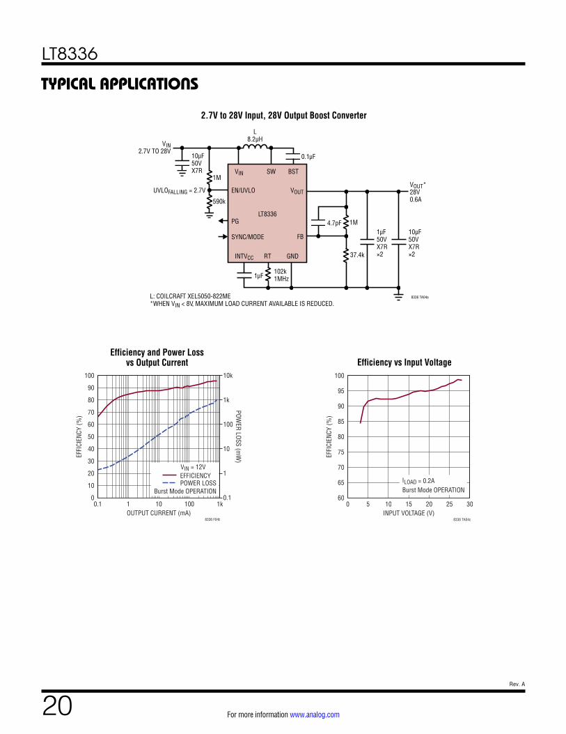
2.7V to 28V Input, 28V Output Boost Converter
TYPICAL APPLICATIONS
Efficiency and Power Loss vs Output Current Efficiency vs Input Voltage
Burst Mode OPERATION
EFFICIENCYPOWER LOSS
OUTPUT CURRENT (mA)0.1 1 10 100 1k
0
10
20
30
40
50
60
70
80
90
100
0.1
1
10
100
1k
10k
EFFI
CIEN
CY (%
)
POWER LOSS (m
W)
8336 F04b
VIN = 12V
Burst Mode OPERATIONILOAD = 0.2A
INPUT VOLTAGE (V)0 5 10 15 20 25 30
60
65
70
75
80
85
90
95
100
EFFI
CIEN
CY (%
)
8336 TA04c
10µF50VX7R×2
1µF50VX7R×2INTVCC
SYNC/MODE
PG
VIN SW BST
EN/UVLO
FB
GND
VOUT
LT8336
RT
L8.2µH
0.1µF
1M
37.4k
1µF102k1MHz
4.7pF
1M
590k
UVLOFALLING = 2.7V
10µF50VX7R
8336 TA04a
VOUT*28V0.6A
L: COILCRAFT XEL5050-822ME*WHEN VIN < 8V, MAXIMUM LOAD CURRENT AVAILABLE IS REDUCED.
VIN2.7V TO 28V

LT8336
21Rev. A
For more information www.analog.com
Automotive Pre-Boost Converter for Stop-Start and Cold Crank with 20V Regulated Output and High Efficiency PassThru Mode
Efficiency vs Input VoltageEfficiency and Power Loss
vs Output Current
TYPICAL APPLICATIONS
L: COILCRAFT XEL5050-223ME*WHEN VIN > 24V, VOUT FOLLOWS VINWHEN VIN <8V, MAXIMUM LOAD CURRENT AVAILABLE IS REDUCED.
10µF50VX7R×4
1µF50VX7R×2INTVCC
SYNC/MODE
PG
VIN SW BST
EN/UVLO
FB
GND
VOUT
LT8336
RT
L22µH
0.1µF
1M
43.2k
1µF267k400kHz
4.7pF
1M
200k
UVLOFALLING = 6V
10µF50VX7R
8336 TA05a
VOUT*20V0.6A
VIN6V TO 40V
EFFICIENCYPOWER LOSS
OUTPUT CURRENT (mA)0.1 1 10 100 1k
0
10
20
30
40
50
60
70
80
90
100
0.1
1
10
100
1k
10k
EFFI
CIEN
CY (%
)
POWER LOSS (m
W)
vs Output Current
8336 TA05b
VIN = 12V
Burst Mode OPERATION Burst Mode OPERATIONILOAD = 0.2A
INPUT VOLTAGE (V)0 5 10 15 20 25 30 35 40
60
65
70
75
80
85
90
95
100
EFFI
CIEN
CY (%
)
Efficiency vs Input Voltage
8336 TA05c

LT8336
22Rev. A
For more information www.analog.com
PACKAGE DESCRIPTIONLQ
FN P
acka
ge16
-Lea
d (3
mm
× 3
mm
× 0
.94m
m)
(Ref
eren
ce L
TC D
WG
# 05
-08-
1626
Rev
A)
DETA
IL B
A
PACK
AGE
TOP
VIEW
5PIN
1CO
RNER
Y
X
aaa
Z2×
16b
PACK
AGE
BOTT
OM V
IEW
46
SEE
NOTE
SE
D
b
0.37
5e
eb
E1
D1
DETA
IL B
SUBS
TRAT
EM
OLD
CAP
// bbb Z
Z
H2H1DE
TAIL
C
SUGG
ESTE
D PC
B LA
YOUT
TOP
VIEW0.0000
0.00
00
0.75
00
0.25
00
0.25
00
0.75
00
0.7500
0.2500
0.2500
0.7500
DETA
IL A
7
SEE
NOTE
S
PIN
1 NO
TCH
0.24
× 4
5°
1316
85
1 4
12 9
aaa Z 2×
MX
YZ
ccc
MXY Z ccc
MX
YZ
eee
MZ
fff
PACK
AGE
OUTL
INE
0.25
REF
0.70
REF
3.50
±0.
05
3.50
±0.
05
LGA
16 0
320
REV
A
TRAY
PIN
1BE
VEL
PACK
AGE
IN T
RAY
LOAD
ING
ORIE
NTAT
ION
COM
PONE
NTPI
N 1
LTXX
XXX
0.37
5
0.38
5
0.37
5
0.38
5
DETA
IL A
ddd Z16×
SYM
BOL
A A1 L b D E D1 E1 e H1 H2 aaa
bbb
ccc
ddd
eee
fff
MIN
0.85
0.01
0.30
0.22
NOM
0.94
0.02
0.40
0.25
3.00
3.00
1.44
1.44
0.50
0.24
REF
0.70
REF
MAX
1.03
0.03
0.50
0.28
0.10
0.10
0.10
0.10
0.15
0.08
NOTE
S
SUBS
TRAT
E TH
KM
OLD
CAP
HT
DIM
ENSI
ONSZ
A1 DETA
IL C
NOTE
S:1.
DIM
ENSI
ONIN
G AN
D TO
LERA
NCIN
G PE
R AS
ME
Y14.
5M-1
994
2. A
LL D
IMEN
SION
S AR
E IN
MIL
LIM
ETER
S
3. P
RIM
ARY
DATU
M -Z
- IS
SEAT
ING
PLAN
E
MET
AL F
EATU
RES
UNDE
R TH
E SO
LDER
MAS
K OP
ENIN
G NO
T SH
OWN
SO
AS
NOT
TO O
BSCU
RE T
HESE
TER
MIN
ALS
AND
HEAT
FEA
TURE
S
54
DETA
ILS
OF P
IN 1
IDEN
TIFI
ER A
RE O
PTIO
NAL,
BUT
MUS
T BE
LO
CATE
D W
ITHI
N TH
E ZO
NE IN
DICA
TED.
THE
PIN
1 ID
ENTI
FIER
M
AY B
E EI
THER
A M
OLD
OR M
ARKE
D FE
ATUR
E
6TH
E EX
POSE
D HE
AT F
EATU
RE M
AY H
AVE
OPTI
ONAL
COR
NER
RADI
I
7CO
RNER
SUP
PORT
PAD
CHA
MFE
R IS
OPT
IONA
L
e
L
e/2
1.44
0.32
5
1.44
0.37
5
0.37
5
0.33
5

LT8336
23Rev. A
For more information www.analog.com
Information furnished by Analog Devices is believed to be accurate and reliable. However, no responsibility is assumed by Analog Devices for its use, nor for any infringements of patents or other rights of third parties that may result from its use. Specifications subject to change without notice. No license is granted by implication or otherwise under any patent or patent rights of Analog Devices.
REVISION HISTORYREV DATE DESCRIPTION PAGE NUMBER
A 11/21 Updated all instances of Pass Through mode to trademarked PassThru.
Added patent reference.Updated AEC-Q100 qualification status.Added with PassThru into Part Title.Clarified titling on typical graph G24.Updated graph descriptions.Updated SYNC/MODE pin description.Removed erroneous pin number.Updated operating description.Edited typical VIN quiescent current.Edited Equation 1 reference to VIN.Edited frequency foldback description.Added LT8337/LT8337-1 to Related Parts section.
1-3, 6, 8, 10, 13-14, 20, 22
1116789
10, 1611111422

LT8336
24Rev. A
For more information www.analog.com ANALOG DEVICES, INC. 2020-2021
11/21www.analog.com
RELATED PARTS
TYPICAL APPLICATION
PART NUMBER DESCRIPTION COMMENTS
LT8330 1A (ISW), 60V, 2MHz High Efficiency Boost/SEPIC/Inverting DC/DC Converter
VIN = 3V to 40V, VOUT(MAX) = 60V, IQ = 6µA (Burst Mode Operation), ISD = < 1µA, ThinSOT, 2mm × 3mm DFN Packages
LT8331 0.5A (ISW), 140V, 500kHz High Efficiency Boost/Flyback/SEPIC/Inverting DC/DC Converter
VIN = 4.5V to 100V, VOUT(MAX) = 135V, IQ = 6µA (Burst Mode Operation), ISD = < 1µA, MSOP-16(12)E
LT8337/LT8337-1 28V, 5A, Low IQ Synchronous Step-Up Silent Switcher with PassThru
VIN = 2.7V to 28V, VOUT(MAX) = 28V, VIN Pin IQ = 4µA (Burst Mode Operation), 3mm × 3mm LQFN package
LT3957A/LT3957 Boost, Flyback, SEPIC and Inverting Converter with 5A/40V Switch
3V ≤ VIN ≤ 40V, Current Mode Control, 100kHz to 1MHz Programmable Operation Frequency, 5mm × 6mm QFN-36 Package
LT3958 High Input Voltage, Boost, Flyback, SEPIC and Inverting Converter with 3.5A/80V Switch
5V ≤ VIN < 80V, Current Mode Control, 100kHz to 1MHz Programmable Operation Frequency, 5mm × 6mm QFN-36 Package
LT8335 28V, 2A, Low IQ Boost/SEPIC/Inverting 2MHz Converter
VIN = 3V to 25V, VOUT(MAX) = 25V, IQ = 6µA (Burst Mode Operation), 3mm × 2mm DFN Package
LT8362 60V, 2A, Low IQ Boost/SEPIC/Inverting 2MHz Converter
VIN = 2.8V to 60V, VOUT(MAX) = 60V, IQ = 9µA (Burst Mode Operation), MSOP-16(12)E, 3mm × 3mm DFN-10 Packages
LT8364 60V, 4A, Low IQ Boost/SEPIC/Inverting 2MHz Converter
VIN = 2.8V to 60V, VOUT(MAX) = 60V, IQ = 9µA (Burst Mode Operation), MSOP-16(12)E, 4mm × 3mm DFN-12 Packages
LT8494 70V, 2A Boost/SEPIC 1.5MHz High Efficiency Step-Up DC/DC Converter
VIN = 1V to 60V (2.5V to 32V Start-Up), VOUT(MAX) = 70V, IQ = 3µA (Burst Mode Operation), ISD = <1µA, 20-Lead TSSOP
LT8580 1A (ISW), 65V 1.5MHz, High Efficiency Step-Up DC/DC Converter
VIN: 2.55V to 40V, VOUT(MAX) = 65V, IQ = 1.2mA, ISD = <1µA, 3mm × 3mm DFN-8, MSOP-8E
Automotive Pre-Boost Converter for Stop-Start and Cold Crank with 10V Regulated Output and High Efficiency PassThru Mode
Efficiency vs Input Voltage
Burst Mode OPERATIONILOAD = 0.5A
INPUT VOLTAGE (V)0 5 10 15 20 25 30 35 40
60
65
70
75
80
85
90
95
100
EFFI
CIEN
CY (%
)
8336 TA06bL: COILCRAFT XEL4020-222ME
*WHEN VIN > 10V, VOUT FOLLOWS VIN WHEN VIN < 8V, MAXIMUM LOAD CURRENT AVAILABLE IS REDUCED
10µF50VX7R×2
1µF50VX7R×2INTVCC
SYNC/MODE
PG
VIN SW BST
EN/UVLO
FB
GND
VOUT
LT8336
RT
L2.2µH
0.1µF
1M
110k
1µF47.5k2MHz
4.7pF
1M
549k
UVLOFALLING = 2.8V
10µF50VX7R
8336 TA06a
VOUT*10V1.5A
VIN2.8V TO 40V