lta460h2-l02
TRANSCRIPT

8/8/2019 LTA460H2-L02
http://slidepdf.com/reader/full/lta460h2-l02 1/27
Date : Oct. 25, 2004
Note :
Any Modification of Spec is not allowed without SEC's permission.
Senior Engineer :
PREPARED BY : AMLCD TECHNICAL CUSTOMER SERVICE TEAM
Samsung Electronics Co . , LTD.
SAMSUNG TFT-LCD
MODEL NO. : LTA460H2-L02
Product Information
Date : Oct. 25, 2004

8/8/2019 LTA460H2-L02
http://slidepdf.com/reader/full/lta460h2-l02 2/27
Doc. No. LTA460H2-L02 Rev. No. 0.0-041025 Page 2 / 27
Product Information
Contents
General Description -------------------------- (3)
1. Absolute Maximum Ratings -------------------------- (4)
1.1 Absolute Ratings Of Environment
1.2 Electrical Absolute Ratings
2. Optical Characteristics -------------------------- (6)
3. Electrical Characteristics -------------------------- (10)
3.1 TFT LCD Module
3.2 Back-light Unit
4. Block Diagram -------------------------- (13)
4.1 TFT LCD Module
4.2 Back-light Unit
5. Input Terminal Pin Assignment -------------------------- (14)
5.1 Input Signal & Power
5.2 Inverter Control Connector
5.2 LVDS Interface5.3 Inverter Unit
5.5 Inverter Specification
5.6 Input Signals, Basic Display Colors and Gray Scale of Each Color
6. Interface Timing -------------------------- (18)
6.1 Timing Parameters (DE only mode)
6.2 Timing Diagrams of interface Signal (DE only mode)
6.3 Power ON/OFF Sequence
6.4 Inverter Power Sequence
7. Outline Dimension -------------------------- (21)
8. Packing --------------------------- (23)
9. Marking & Others --------------------------- (24)
10. General Precautions --------------------------- (26)

8/8/2019 LTA460H2-L02
http://slidepdf.com/reader/full/lta460h2-l02 3/27
Doc. No. LTA460H2-L02 Rev. No. 0.0-041025 Page 3 / 27
Product Information
General Description
* Description
LTA460H2-L02 is a color active matrix TFT (Thin Film Transistor) liquid crystal display
(LCD) that uses amorphous silicon TFTs as a switching devices. This model is composed of a
TFT LCD panel, a driver circuit and a back-light system. The resolution of a 46.0" contains
1920 x 1080 pixels and can display up to 16.7 million colors with wide viewing angle of 85°
or higher in all directions.
* Features
- High contrast ratio, high aperture structure- PVA(Patterned Vertical Align) mode
- Wide viewing angle(±170°)
- High speed response
- WUXGA(1920 x 1080 pixels) resolution (16:9)
- Low Power consumption
- Direct Type 24 CCFT( Cold Cathode Fluorescent Tube)
- DE only mode
- 2Channels LVDS(Low-Voltage Differential Signal) interface.(2 pixels/clock)
* Applications
Home-alone Multimedia TFT-LCD TV
Display terminals for AV application products
High Definition TV (HD TV)
* General information
Items Specification Unit Note
Display area 1018.08(H) x 572.67(V) mm
Driver element a-Si TFT active matrix
Display colors 16.7M(true) colors
Number of pixels 1920 x 1080 pixel 16:9
Pixel arrangement RGB Vertical Stripe
Pixel pitch 0.17675(H) × 0.53025(W) mm
Display mode Normally Black
Surface treatment Haze 44% , Hard-Coati ng (3H) Anti -Gl are

8/8/2019 LTA460H2-L02
http://slidepdf.com/reader/full/lta460h2-l02 4/27
Doc. No. LTA460H2-L02 Rev. No. 0.0-041025 Page 4 / 27
Product Information
* Mechanical information (Panel Module Only)
1. Absolute Maximum Ratings
1.1 Absolute ratings of environment
Note (1) Temperature and relative humidity range are shown in the figure below.90 % RH Max. ( 40 °C ≥ Ta )
Maximum wet-bulb temperature at 39 ° C or less. (Ta > 40 ° C) No condensation.
(2) 11ms, sine wave, 1 time for ±X, ±Y, ±Z axis
(3) 10-300 Hz, Sweep rate 10min, 30min for X,Y,Z axis
(4) At testing Vibration and Shock, the fixture in holding the Module to be tested have
to be hard and rigid enough so that the Module would not be twisted or bent by the
fixture.
0
20
40
60
80
100
-40 -20 0 20 40 60 80
5
90
Operating Range
Storage Range
Relative Humidity ( %RH)
Temperature (OC)
Item Min. Typ. Max. Note
Module
size
Horizontal(H) 1082.0 1083.0 1084.0 mm
Vertical(V) 626.0 627.0 628.0 mm
Depth(D) 55.5 56.5 57.5 mm
Weight 12,000 13,500 15,000 g
Item Symbol Min. Max. Unit Note
Storage temperature TSTG -20 65 ℃ (1)
Operating temperature
(Ambient temperature)TOPR 0 50 ℃ (1)
Shock ( non - operating ) Snopx,y axis - 50 G
(2),(4)z axis - 35 G
Vibration ( Non - operating ) Vnop - 1.5 G (3),(4)

8/8/2019 LTA460H2-L02
http://slidepdf.com/reader/full/lta460h2-l02 5/27
Doc. No. LTA460H2-L02 Rev. No. 0.0-041025 Page 5 / 27
Product Information
1.2 ELECTRICAL ABSOLUTE RATINGS
(1) TFT LCD Module (Vss = GND = 0 V)
Item Symbol Min. Max. Unit Note
Power Supply Voltage VDD Vss-0.5 5.5 V (1)
NOTE (1) Within Ta ( 25 ± 2 °C)
(2) BACK-LIGHT UNIT (Ta = 25 ± 2°C)
Item Symbol Min. Max. Unit. Note
Lamp Current IL
4.0 7.0 mArms (1),(2)Lamp Frequency FL 40 80 kHz (1)
NOTE (1) Permanent damage to the device may occur if maximum values are exceeded.
Functional operation should be restricted to the conditions described under
Normal Operating Conditions.
(2) Specified values are for a single lamp.

8/8/2019 LTA460H2-L02
http://slidepdf.com/reader/full/lta460h2-l02 6/27
Doc. No. LTA460H2-L02 Rev. No. 0.0-041025 Page 6 / 27
Product Information
2. Optical Characteristics
The following items are measured under stable conditions. The optical characteristics should be
measured in a dark room or equivalent state with the methods shown in Note (1).
◆ Measuring equipment : TOPCON BM-5A , BM-7, PHOTO RESEARCH PR650
EZ-Contrast (Eldim)
* Ta = 25 ± 2°C , VDD=5V, fv= 60Hz, f DCLK=74.25 MHz, IL = 5.5 mArms
Item Symbol Condition Min. Typ. Max. Unit Note
Contrast Ratio
(Center of screen) C/R
Normal
φ = 0
θ = 0
Viewing
Angle
600 800 -
(3)
BM-5A
Response
Time
Rising Tr - 3.5 10msec
(4)
BM-7Falling Tf - 4.5 10
Luminance of White
(Center of screen)YL 400 450 - cd/m2
(5)
BM-5A
Color
Chromaticity
(CIE 1931)
RedRx
TYP.-0.03
0.648
TYP.+0.03
(6)PR650
Ry 0.333
GreenGx 0.271
Gy 0.592
BlueBx 0.141
By 0.066
WhiteWx 0.280
Wy 0.290
Lamp Temperature - 10,000 - K
Viewing
Angle
Hor.θ L
C/R≥10
75 85 -
Degrees(7)
BM-5A
θ R 75 85 -
Ver. φ H 75 85 -φ L 75 85 -
Brightness Uniformity
(9 points)Buni - - 25 %
(2),(8)
BM-5A

8/8/2019 LTA460H2-L02
http://slidepdf.com/reader/full/lta460h2-l02 7/27
Doc. No. LTA460H2-L02 Rev. No. 0.0-041025 Page 7 / 27
Product Information
Note 1) Test Equipment Setup
After stabilizing and leaving the panel alone at a given temperature for 30 min ,the
measurement should be executed. Measurement should be executed in a stable, windless, and
dark room 30 min after lighting the back-light. This should be measured in the center of
screen.
A single lamp current : 5.5 mA
Environment condition : Ta = 25 ± 2 °C
Photodetector
Photodetector Field
BM-5A 2°
BM-7 2°
PR650 1°
LCD Panel
TFT - LCD Module
The center of the screen
BM-5A : 40㎝
BM-7 : 50㎝
PR650 : 50㎝
Field
Optical Measuring Equipment Setup
Note 2) Definition of test point
①③
④
②
⑤
320 960 1600
Active Area
Test Point
180
540
900
⑥
⑨ ⑧ ⑦
50

8/8/2019 LTA460H2-L02
http://slidepdf.com/reader/full/lta460h2-l02 8/27
Doc. No. LTA460H2-L02 Rev. No. 0.0-041025 Page 8 / 27
Product Information
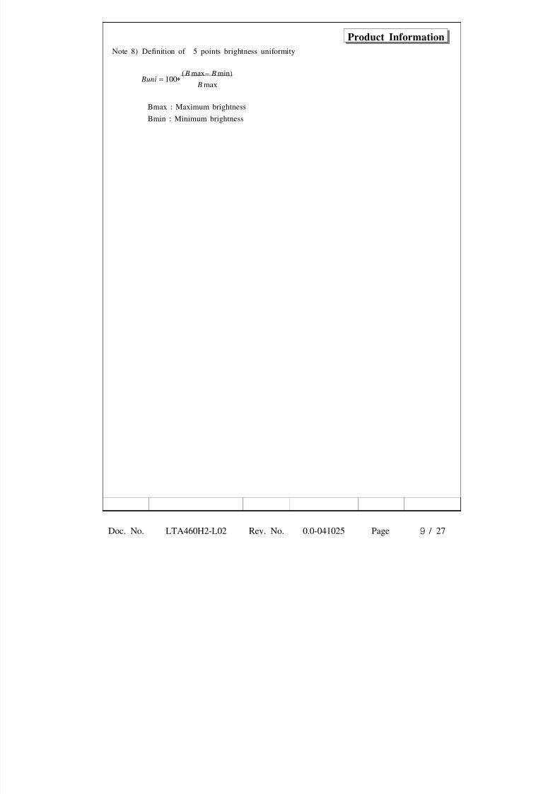
Note 3) Definition of Contrast Ratio (C/R) : Ratio of gray max (Gmax) & gray min (Gmin)
at the center point(5) of the panel
CRG
G=
max
min
Gmax : Luminance with all pixels white
Gmin : Luminance with all pixels black
Note 4) Definition of Response time : Sum of Tr ,Tf
Display data White(TFT ON)Black(TFT OFF) Black(TFT OFF)
Optical
Response
100%90%
10%
0%
TR TF
Time
Note 5) Definition of Luminance of White : Luminance of white at center point(5).
Note 6) Definition of Color Chromaticity (CIE 1931)Color coordinate of Red , Green , Blue & White at center point(5).
Note 7) Definition of Viewing Angle : Viewing angle range (CR≥10 )
6 O’clock
direction
Norm al L ine
θ L
θ R
φ Hφ L 12 O’c lock direction
θR =90o
θ L =9 0o
φ = 0o,
x
x’y ’
y
θ = 0o
φ H = 90o
φ L= 9 0o
8/8/2019 LTA460H2-L02
http://slidepdf.com/reader/full/lta460h2-l02 9/27

8/8/2019 LTA460H2-L02
http://slidepdf.com/reader/full/lta460h2-l02 10/27
Doc. No. LTA460H2-L02 Rev. No. 0.0-041025 Page 10 / 27
Product Information
3. Electrical Characteristics
3.1 TFT LCD MODULE Ta = 25°C
Item Symbol Min. Typ. Max. Unit Note
Voltage of Power Supply 4.5 5.0 5.5 V (1)
Current of
Power
Supply
(a)Black
IDD
- 2000 - mA (2),(3)
(Without
Inverter)
(b)Mosaic - 2200 - mA
(d)N-Pattern - 3200 3500 mA
Vsync Frequency f V - 60 - Hz
Hsync Frequency f H 65.5 67.5 69.5 kHz
Main Frequency f DCLK 131 74.25 166.8 MHz
Rush Current IRUSH - 4.5 6 A (4)
Note (1) Voltage of Power Supply is the value which is measured at the input connector of panel.
(2) f V=60Hz, f DCLK =74.25MHz, VDD = 5.0V, DC Current.
(3) Power dissipation check pattern(LCD Module only)
(a) Black Pattern (b) Mosaic Pattern
(c) N-pattern

8/8/2019 LTA460H2-L02
http://slidepdf.com/reader/full/lta460h2-l02 11/27
Doc. No. LTA460H2-L02 Rev. No. 0.0-041025 Page 11 / 27
Product Information
(4) Measurement Conditions (Rising time =470㎲)
Note : Control Signal : High(+5V) -->Low(Ground)
All Signal lines to panel except for power 5V : Ground
The rising time of supplied voltage is controlled to 470us by R and C value.
0.9 VDD
0.1 VDD
Rising Time
GND
5V
A
1㎌
1㎌
47㏀
47㏀
2SK1339
2SK1059
1㏀
0.01㎌
VDD
INPUT
POWER(5V)
12V
CONTROLSIGNAL(High to
Low)
Test Poi nt
RC

8/8/2019 LTA460H2-L02
http://slidepdf.com/reader/full/lta460h2-l02 12/27
Doc. No. LTA460H2-L02 Rev. No. 0.0-041025 Page 12 / 27
Product Information
3.2 BACK-LIGHT UNIT
The back-light system is an direct - lighting type with 24 CCFTs ( Cold Cathode
Fluorescent Tube ) The characteristics of 24 direct lamps are shown in the following tables.
Ta=25 ± 2°C
Item Symbol Min. Typ. Max. Unit Note
Lamp Current IL 4.0 6.0 7.0 mArms (1)
Lamp Voltage VL 1480 1540 1600 Vrms (1)
Lamp Frequency f L 40 - 80 kHz (2)
Operating Life Time Hr 50,000 - - Hour (3)
Start up Voltage Vs - -0℃:2500
Vrms (4)
25℃:1990
Note) The waveform of the inverter output voltage must be area symmetric and the design
of the inverter must have specifications for the modularized lamp.
Specified values are for a single lamp.
The performance of the back-light, for example life time or brightness, is much influenced by
the characteristics of the DC-AC inverter for the lamp. So all the parameters of an inverter
should be carefully designed so as not to produce too much leakage current from high-voltage
output of the inverter.
When you design or order the inverter, please make sure that a poor lighting caused by the
mismatch of the back-light and the inverter(miss lighting, flicker, etc.) never occur. When you
confirm it, the module should be operated in the same condition as it is installed in your
instrument.
Note (1) lamp current is measured with current meter.
Refer to the block diagram of the back-light unit in the next page for more information.
Lamp Voltage Min : Lamp Current 7.0 mArms
Lamp Voltage Max : Lamp Current 4.0 mArms
(2) Lamp frequency may produce interference with horizontal synchronous frequency and this
may cause line flow on the display. Therefore lamp frequency shall be detached from
the horizontal synchronous frequency and its harmonics as far as possible in order to
avoid interference.
(3) Life time (Hr) of a lamp is defined as the time in which it continues to operate under
the condition of Ta = 25±2°C and IL = 5.5mArms for a lamp until the brightness
becomes 50% or lower than it's original value.
(4) If an inverter has shutdown function it should keep its output for more than 1 second
even if the lamp connector open. Otherwise the lamps may not to be turned on.

8/8/2019 LTA460H2-L02
http://slidepdf.com/reader/full/lta460h2-l02 13/27
Doc. No. LTA460H2-L02 Rev. No. 0.0-041025 Page 13 / 27
Product Information
4. Block Diagram
4.1 TFT LCD MODULE
DC-DC BLOCK
& Gamma Generation
Timing
Controller
( MERGED
LVDS )
SOURCE DRIVE IC
(S6C2101,384CH)
x 10 EA
GATE DRIVE IC
(KS0655, 128CH)
x 6 EA
CPV,OE,STV
Control Signal (TP, POL, STH)
VON,VOFF,DVDD(5V) DC-DC BLOCK
& Gamma Generation
Timing
Controller
( MERGED
LVDS )
LVDS 2ch
M A I N P
O W E R
C O N N E C T O R
SOURCE DRIVE IC
(S6C2104,414CH)
x 14 EA
GATE DRIVE IC
(S6CG105, 135CH)
x 8 EA x 2 Bank
R S D S S i g n a l
CPV,OE,STV
Control Signal (TP, POL, STH)
VON,VOFF,DVDD
M E M
O R Y
M E M
O R Y
T e r m i n a t i o n
R e s i s t
o r
4.2 BACK-LIGHT UNIT
HOT 1
HOT 2
CCFL1,2
CCFL3,4HOT 3
HOT 4
CCFL21,22
CCFL23,24
HOT 21
HOT 22
HOT 23
HOT 24
HOT 1
HOT 2
HOT 3
HOT 4
HOT 21
HOT 22
HOT 23
HOT 24
HOT 사양 : HI GH VOLTAGE

8/8/2019 LTA460H2-L02
http://slidepdf.com/reader/full/lta460h2-l02 14/27
Doc. No. LTA460H2-L02 Rev. No. 0.0-041025 Page 14 / 27
Product Information
5. Input Terminal Pin Assignment
5.1. Input Signal & Power : Connector 30P, FI-E30S
5.2. Inverter Control ConnectorConnector : JST S14B-PH-SM3
Connector : JST S14B-PH-SM3
No Signal
1 D 24V
2 D 24V
3 D 24V
4 D 24V
5 D 24V
6 GND
7 GND
8 GND
9 GND
10 GND
11 N.C
12 Inverter Enable (On : 5V, Off : 0V)
13 ADIM [Max : 3.3V, Min : 0V]
14 PDIM [Max : 100%, Min : 30%]
No Signal No Signal
1 RxInO0- 16 RxInE2+
2 RxInO0+ 17 RxInECLK-
3 RxInO1- 18 RxInECLK+
4 RxInO1+ 19 RxInE3-
5 RxInO2- 20 RxInE3+
6 RxInO2+ 21 GND
7 RxInOCLK- 22 GND
8 RxInOCLK+ 23 GND
9 RxInO3- 24 GND
10 RxInO3+ 25 GND
11 RxInE0- 26 VDD(=+5[V])
12 RxInE0+ 27 VDD(=+5[V])
13 RxInE1- 28 VDD(=+5[V])
14 RxInE1+ 29 VDD(=+5[V])
15 RxInE2- 30 VDD(=+5[V])

8/8/2019 LTA460H2-L02
http://slidepdf.com/reader/full/lta460h2-l02 15/27
Doc. No. LTA460H2-L02 Rev. No. 0.0-041025 Page 15 / 27
Product Information
5.3. Inverter Input Power Sequence
Vin
ADIM Control Range : 0 ~ 3.3V
On/Off
∼
PWM
0.5sec(Min)
0.5sec(Min)
0.5sec(min) PWM High 0.1sec(Min)
0.5sec(Min)
Vin
ADIM Control Range : 0 ~ 3.3V
On/Off
∼
PWM
0.5sec(Min)
0.5sec(Min)
0.5sec(min) PWM High 0.1sec(Min)
0.5sec(Min)

8/8/2019 LTA460H2-L02
http://slidepdf.com/reader/full/lta460h2-l02 16/27
Doc. No. LTA460H2-L02 Rev. No. 0.0-041025 Page 16 / 27
Product Information
5.4 Inverter Specification
Note(1) Controlled by Analog or PWM dimming
Note(2) High-duty = On/(On+Off) * 100
Note(3) - Controlled by Analog dimming only
- Analog dimming 0[V] (Minimum Lamp current)
- Analog dimming 3.3[V] (Maximum Lamp current)
On Off
Items Symbol ConditionsSpecifications
Unit 비고Min. Typ. Max.
Input Power Vin - 23 24 25 V Ta=25℃
Input Current Iin Vin=24V, Adim=3.3V (TBD) Adc
Output Current
(Single Lamp)
Io,max Adim=3.3V (6.5) (7.0) (7.5)mArms
After 2hour
Warm-up,
Note (1)Io.min Adim=0V (3.5) (4.0) (4.5)
Frequency FL Vin=24V,Adim=3.3V (55) (60) (65) kHz
Open Lamp
Shutdown TimeTs-d No Load 1.0 1.5 2.0 sec
Open Lamp
VoltageVo
Vin=24V,ADIM=3.3V
Each Transformer
Output
(1400) V
On/Off controlOn ON/OFF=High 2.4 - 5.25 V
Off ON/OFF=Low 0 - 0.8 V
PWM signalVpwm ON(high) 2.4 5.25 V
Vpwm OFF(low) 0 0.8 V
PWM duty PDVin=24V,Adim=3.3V 30 100
% Note (2)Vin=24V,Adim=0V 50 100
Analog Dimmer
Max Lum - - 3. 3 -
V Note (3)Min. Lum - - 0 -

8/8/2019 LTA460H2-L02
http://slidepdf.com/reader/full/lta460h2-l02 17/27
Doc. No. LTA460H2-L02 Rev. No. 0.0-041025 Page 17 / 27
Product Information
5.5 Input Signal,Basic Display Colors and Gray Scale of Each Color
Note) Definition of Gray :
Rn : Red Gray, Gn : Green Gray, Bn : Blue Gray (n = Gray level)
Input Signal : 0 = Low level voltage, 1 = High level voltage
COLOR DISPLAY
DATA SIGNAL GRAY
SCALE
LEVEL
RED GREEN BLUE
R0 R1 R2 R3 R4 R5 R6 R7 G0 G1 G2 G3 G4 G5 G6 G7 B0 B1 B2 B3 B4 B5 B6 B7
BASIC
COLOR
BLACK 0 0 0 0 0 0 0 0 0 0 0 0 0 0 0 0 0 0 0 0 0 0 0 0 -
BLUE 0 0 0 0 0 0 0 0 0 0 0 0 0 0 0 0 1 1 1 1 1 1 1 1 -
GREEN 0 0 0 0 0 0 0 0 1 1 1 1 1 1 1 1 0 0 0 0 0 0 0 0 -
CYAN 0 0 0 0 0 0 0 0 1 1 1 1 1 1 1 1 1 1 1 1 1 1 1 1 -
RED 1 1 1 1 1 1 1 1 0 0 0 0 0 0 0 0 0 0 0 0 0 0 0 0 -
MAGENTA 1 1 1 1 1 1 1 1 0 0 0 0 0 0 0 0 1 1 1 1 1 1 1 1 -
YELLOW 1 1 1 1 1 1 1 1 1 1 1 1 1 1 1 1 0 0 0 0 0 0 0 0 -
WHITE 1 1 1 1 1 1 1 1 1 1 1 1 1 1 1 1 1 1 1 1 1 1 1 1 -
GRAY
SCALE
OF RED
BLACK 0 0 0 0 0 0 0 0 0 0 0 0 0 0 0 0 0 0 0 0 0 0 0 0 R0
DARK
↑
↓
LIGHT
1 0 0 0 0 0 0 0 0 0 0 0 0 0 0 0 0 0 0 0 0 0 0 0 R1
0 1 0 0 0 0 0 0 0 0 0 0 0 0 0 0 0 0 0 0 0 0 0 0 R2
: : : : : : : : : : : : : : : : : : : : : : : : R3~
R252: : : : : : : : : : : : : : : : : : : : : : : :
1 0 1 1 1 1 1 1 0 0 0 0 0 0 0 0 0 0 0 0 0 0 0 0 R253
0 1 1 1 1 1 1 1 0 0 0 0 0 0 0 0 0 0 0 0 0 0 0 0 R254
RED 1 1 1 1 1 1 1 1 0 0 0 0 0 0 0 0 0 0 0 0 0 0 0 0 R255
GRAY
SCALE
OF
GREEN
BLACK 0 0 0 0 0 0 0 0 0 0 0 0 0 0 0 0 0 0 0 0 0 0 0 0 G0
DARK
↑
↓
LIGHT
0 0 0 0 0 0 0 0 1 0 0 0 0 0 0 0 0 0 0 0 0 0 0 0 G1
0 0 0 0 0 0 0 0 0 1 0 0 0 0 0 0 0 0 0 0 0 0 0 0 G2
: : : : : : : : : : : : : : : : : : : : : : : : G3~
G252: : : : : : : : : : : : : : : : : : : : : : : :
0 0 0 0 0 0 0 0 1 0 1 1 1 1 1 1 0 0 0 0 0 0 0 0 G253
0 0 0 0 0 0 0 0 0 1 1 1 1 1 1 1 0 0 0 0 0 0 0 0 G254
GREEN 0 0 0 0 0 0 0 0 1 1 1 1 1 1 1 1 0 0 0 0 0 0 0 0 G255
GRAY
SCALE
OF
BLUE
BLACK 0 0 0 0 0 0 0 0 0 0 0 0 0 0 0 0 0 0 0 0 0 0 0 0 B0
DARK
↑
↓
LIGHT
0 0 0 0 0 0 0 0 0 0 0 0 0 0 0 0 1 0 0 0 0 0 0 0 B1
0 0 0 0 0 0 0 0 0 0 0 0 0 0 0 0 0 1 0 0 0 0 0 0 B2
: : : : : : : : : : : : : : : : : : : : : : : : B3~
B252: : : : : : : : : : : : : : : : : : : : : : : :
0 0 0 0 0 0 0 0 0 0 0 0 0 0 0 0 1 0 1 1 1 1 1 1 B253
0 0 0 0 0 0 0 0 0 0 0 0 0 0 0 0 0 1 1 1 1 1 1 1 B254
BLUE 0 0 0 0 0 0 0 0 0 0 0 0 0 0 0 0 1 1 1 1 1 1 1 1 B255

8/8/2019 LTA460H2-L02
http://slidepdf.com/reader/full/lta460h2-l02 18/27
Doc. No. LTA460H2-L02 Rev. No. 0.0-041025 Page 18 / 27
Product Information
6. Interface Timing
6.1 Timing Parameters ( DE only mode )
SIGNAL ITEM SYMBOL MIN. TYP. MAX. UNIT NOTE
Clock
Frequency 1/TC 65.5 74.25 83.4 ㎒
2pixels/clock
Hgh Time TCH 4 - - nsec
Low Time TCL 4 - - nsec
DataSetup Time TDS 4 - - nsec
Hold Time TDH 4 - - nsec
Data Enable Setup Time TES 4 - - nsec
Frame Frequency Cycle Tv - 16.7 - msec
Vertical Active
Display Term
Display Period TVD - 1080 - lines
Vertical Total TVB 1092 1125 1158 lines
Horizontal Active
Display Term
Display Period THD - 1920 - clocks
Horizontal
TotalTH 2000 2200 2400 clocks

8/8/2019 LTA460H2-L02
http://slidepdf.com/reader/full/lta460h2-l02 19/27
Doc. No. LTA460H2-L02 Rev. No. 0.0-041025 Page 19 / 27
Product Information
6.2 Timing diagrams of interface signal ( DE only mode )
DATA
SIGNALS
DE
TVD
TV
TH
DCLK
TC
DE
THD
TVB
0.5 VCC
TES
TDS TDH
TCH TCL
TC
DE
DISPLAY
DATA
DCLK
0.5 VCC
0.5 VCC

8/8/2019 LTA460H2-L02
http://slidepdf.com/reader/full/lta460h2-l02 20/27
Doc. No. LTA460H2-L02 Rev. No. 0.0-041025 Page 20 / 27
Product Information
6.3 Power ON/OFF Sequence
: To prevent a latch-up or DC operation of the LCD module, the power on/off sequence
should be as the diagram below.
Power SupplyVDD
0.9 VDD 0.9 VDD
0V
0 V
VALID
Signals
T3
0 ≤T1 ≤ 10msec
0 ≤ T2 ≤ 50 msec
0 ≤ T3 ≤ 50 msec
1sec ≤ T4
T1
T2T4
0.1 VDD 0.1 VDD
Back-light(Recommended)
500 msec ≤ T5
100 msec ≤ T6
Power On Power Off
T5 T6
50% 50%
Power ON/OFF Sequence
NOTE
(1)The supply voltage of the external system for the module input should be the
same as the definition of VDD.
(2) Apply the lamp voltage within the LCD operation range. When the back-light turnson before the LCD operation or the LCD turns off before the back-light turns off,
the display may momentarily become abnormal screen.
(3) In case of VDD = off level, please keep the level of input signals on the low or
keep a high impedance.
(4) T4 should be measured after the module has been fully discharged between
power off and on period.
(5) Interface signal shall not be kept at high impedance when the power is on.

8/8/2019 LTA460H2-L02
http://slidepdf.com/reader/full/lta460h2-l02 21/27
7. Outline Dimension - Front side
Doc . No LTA460H2-L02 Rev.No. 0.0-041025
LTA460H2-L02

8/8/2019 LTA460H2-L02
http://slidepdf.com/reader/full/lta460h2-l02 22/27
- Rear side
Doc . No LTA460H2-L02 Rev.No. 0.0-041025
LTA460H2-L02

8/8/2019 LTA460H2-L02
http://slidepdf.com/reader/full/lta460h2-l02 23/27
Doc. No. LTA460H2-L02 Rev. No. 0.0-041025 Page 23 / 27
Product Information
8. Packing
8.1. CARTON(Internal Package)
(1) Packing Form
Corrugated fiberboard box and corrugated cardboard as shock absorber
(2) Packing Method
LCD Module
Cushion-Foam
Cushion-Foam
Pallet
Packing
-PalletBox → Direction: be able to open it
8.2. Packing Specification
ITEM Specification Remark
LCD Packing10ea /
(Packing-Pallet Box)
1. 140 Kg / LCD (10ea)
2. 10 Kg / Cushion-Foam (2ea)
3. 8 Kg / Packing-Pallet Box (1ea)
3. Cushion-Foam Material : EPS
4. Packing-Pallet Box Material : DW4
Pallet 1Box / Pallet 1. Pallet weight = 8.8kg
2. 8.8 Kg / Pallet
Packing Direction Vertical
Total Pallet size H x V x height 1270mm(H) x 1150mm(V) x 844mm(height)
Total Pallet weight 167kgPallet(8.8kg) + Module(14*10=140) +
Cushion(up+botton=10kg) + PALLET-BOX(8kg)

8/8/2019 LTA460H2-L02
http://slidepdf.com/reader/full/lta460h2-l02 24/27
Doc. No. LTA460H2-L02 Rev. No. 0.0-041025 Page 24 / 27
Product Information
9. Marking & Others
A nameplate bearing followed by is affixed to a shipped product at the
specified location on each product.
(1) Parts number : LTA460H2-L02-XXXX
(2) Revision : One letter
(3) Control : One letter
(4) Lot number : 6 D 4 H 123 01 A
1 2 3 4 5 6 7
(5) Nameplate Indication
0408
LTA460H2-L02
MADE IN KOREA 6D4H12301A
① 6 : Line
② D : Device
③ 4 : Year
④ H : Month
⑤ 123 : LOT NO
⑥ 01 : GLASS NO
⑦ A : CELL NO

8/8/2019 LTA460H2-L02
http://slidepdf.com/reader/full/lta460h2-l02 25/27
Doc. No. LTA460H2-L02 Rev. No. 0.0-041025 Page 25 / 27
Product Information
(6) Bar code marking for Customer
The bar code marking is attached to module backside.
1) MODEL NAME : LTA460H2-L02-XXXX
2) SAMSUNG
3) MADE IN KOREA
4) PRODUCTION NUMBER
5) USER MODEL NAME
Bar code shows a) user model name, b) production number
a) User model nameLTA460H2-L02-XXXX
b) Production Number
SAMSUNG
MADE IN KOREA
(7) Packing box attach
SERIAL NO
B REVISION CODE
PRODU CTION MON TH
PRODU CTION YEAR*6430008B*
MA D E IN KOR EA
DE V I CE : LT A460H 2 -L02
T YPE :
QU AN T T Y : 1 PCS
CO6040001

8/8/2019 LTA460H2-L02
http://slidepdf.com/reader/full/lta460h2-l02 26/27
Doc. No. LTA460H2-L02 Rev. No. 0.0-041025 Page 26 / 27
Product Information10. General Precautions
10.1 Handling
(a) When the module is assembled, It should be attached to the system firmly
using every mounting holes. Be careful not to twist and bend the modules.
(b) Refrain from strong mechanical shock and / or any force to the module. In
addition to damage, this may cause improper operation or damage to the module
and CCFT back-light.
(c) Note that polarizers are very fragile and could be easily damaged. Do not press
or scratch the surface harder than a HB pencil lead.
(d) Wipe off water droplets or oil immediately. If you leave the droplets for a long
time, Staining and discoloration may occur.
(e) If the surface of the polarizer is dirty, clean it using some absorbent cotton or
soft cloth.
(f) The desirable cleaners are water, IPA(Isopropyl Alcohol) or Hexane.
Do not use Ketone type materials(ex. Acetone), Ethyl alcohol, Toluene, Ethyl
acid or Methyl chloride. It might permanent damage to the polarizer due to
chemical reaction.
(g) If the liquid crystal material leaks from the panel, it should be kept awayfrom the eyes or mouth . In case of contact with hands, legs or clothes, it must
be washed away thoroughly with soap.
(h) Protect the module from static , it may cause damage to the CMOS Gate Array IC.
(i) Use finger-stalls with soft gloves in order to keep display clean during the
incoming inspection and assembly process.
(j) Do not disassemble the module.
(k) Do not pull or fold the lamp wire.
(l) Do not adjust the variable resistor which is located on the module.
(m) Protection film for polarizer on the module shall be slowly peeled off just before use
so that the electrostatic charge can be minimized.
(n) Pins of I/F connector shall not be touched directly with bare hands.
8/8/2019 LTA460H2-L02
http://slidepdf.com/reader/full/lta460h2-l02 27/27
Product Information10.2 Storage
(a) Do not leave the module in high temperature, and high humidity for a long time.
It is highly recommended to store the module with temperature from 0 to 35C
and relative humidity of less than 70%.
(b) Do not store the TFT-LCD module in direct sunlight.
(c) The module shall be stored in a dark place. It is prohibited to apply sunlight or
fluorescent light during the store.
10.3 Operation
(a) Do not connect,disconnect the module in the "Power On" condition.
(b) Power supply should always be turned on/off by the item 6.3
"Power on/off sequence"
(c) Module has high frequency circuits. Sufficient suppression to the
electromagnetic interference shall be done by system manufacturers. Grounding
and shielding methods may be important to minimize the interference.
(d) The cable between the back-light connector and its inverter power supply shall
be a minimized length and be connected directly . The longer cable between
the back-light and the inverter may cause lower luminance of lamp(CCFT) and
may require higher startup voltage(Vs).
10.4 Others
(a) Ultra-violet ray filter is necessary for outdoor operation.
(b) Avoid condensation of water. It may result in improper operation or disconnection
of electrode.
(c) Do not exceed the absolute maximum rating value. ( the supply voltage variation,
input voltage variation, variation in part contents and environmental temperature,and so on) Otherwise the module may be damaged.
(d) If the module displays the same pattern continuously for a long period of time,it
can be the situation when the image "Sticks" to the screen.
We recommend that you should discuss SEC when you want the module to be
operated in displaying the same pattern for a long time.
(e) This module has its circuitry PCB's on the rear side and should be handled
carefully in order not to be stressed.