ltc4124 (rev. a) · vntc(hys) ntc thresholds hysteresis % of vcc 5 % r ntc(open) ntc open circuit...
TRANSCRIPT
LTC4124
1Rev. A
For more information www.analog.comDocument Feedback
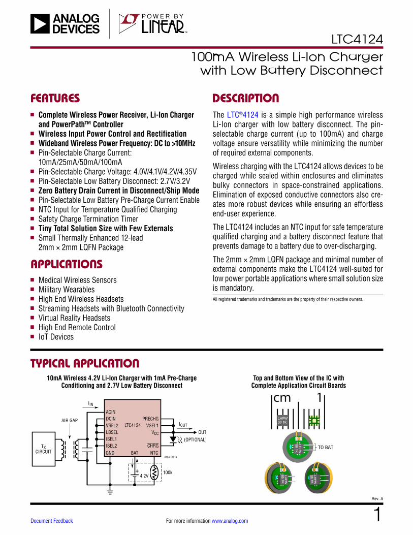
TYPICAL APPLICATION
FEATURES DESCRIPTION
100mA Wireless Li-Ion Charger with Low Battery Disconnect
The LTC®4124 is a simple high performance wireless Li-Ion charger with low battery disconnect. The pin-selectable charge current (up to 100mA) and charge voltage ensure versatility while minimizing the number of required external components.
Wireless charging with the LTC4124 allows devices to be charged while sealed within enclosures and eliminates bulky connectors in space-constrained applications. Elimination of exposed conductive connectors also cre-ates more robust devices while ensuring an effortless end-user experience.
The LTC4124 includes an NTC input for safe temperature qualified charging and a battery disconnect feature that prevents damage to a battery due to over-discharging.
The 2mm × 2mm LQFN package and minimal number of external components make the LTC4124 well-suited for low power portable applications where small solution size is mandatory.
APPLICATIONS
n Complete Wireless Power Receiver, Li-Ion Charger and PowerPath™ Controller
n Wireless Input Power Control and Rectification n Wideband Wireless Power Frequency: DC to >10MHz n Pin-Selectable Charge Current:
10mA/25mA/50mA/ 100mA n Pin-Selectable Charge Voltage: 4.0V/4.1V/4.2V/4.35V n Pin-Selectable Low Battery Disconnect: 2.7V/3.2V n Zero Battery Drain Current in Disconnect/Ship Mode n Pin-Selectable Low Battery Pre-Charge Current Enable n NTC Input for Temperature Qualified Charging n Safety Charge Termination Timer n Tiny Total Solution Size with Few Externals n Small Thermally Enhanced 12-lead
2mm × 2mm LQFN Package
n Medical Wireless Sensors n Military Wearables n High End Wireless Headsets n Streaming Headsets with Bluetooth Connectivity n Virtual Reality Headsets n High End Remote Control n IoT Devices
All registered trademarks and trademarks are the property of their respective owners.
TXCIRCUIT
LTC4124
4124 TA01a
PRECHGVSEL1
VCC
CHRG
ACINDCINVSEL2LBSELISEL1ISEL2GND BAT NTC
OUT
IOUT
IIN
+ 100k4.2V
AIR GAP
(OPTIONAL)
10mA Wireless 4.2V Li-Ion Charger with 1mA Pre-Charge Conditioning and 2.7V Low Battery Disconnect
TO BAT
Top and Bottom View of the IC with Complete Application Circuit Boards
LTC4124
2Rev. A
For more information www.analog.com
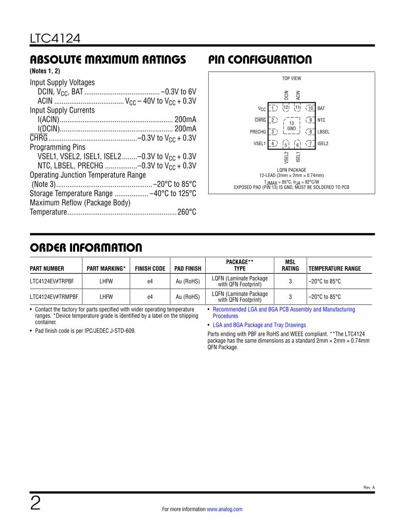
PIN CONFIGURATIONABSOLUTE MAXIMUM RATINGS
Input Supply Voltages DCIN, VCC, BAT ........................................ –0.3V to 6V ACIN ..................................... VCC – 40V to VCC + 0.3VInput Supply Currents I(ACIN) ............................................................ 200mA I(DCIN) ............................................................ 200mA CHRG ...............................................–0.3V to VCC + 0.3VProgramming Pins VSEL1, VSEL2, ISEL1, ISEL2 ........–0.3V to VCC + 0.3V NTC, LBSEL, PRECHG .................–0.3V to VCC + 0.3V Operating Junction Temperature Range (Note 3) ................................................... –20°C to 85°CStorage Temperature Range .................. –40°C to 125°CMaximum Reflow (Package Body) Temperature .......................................................... 260°C
(Notes 1, 2)TOP VIEW
VCC
CHRG
PRECHG
VSEL1
BAT
NTC
LBSEL
ISEL2
DCIN
ACIN
VSEL
2
ISEL
1
10
9
8
7
1
2
3
4
LQFN PACKAGE12-LEAD (2mm × 2mm × 0.74mm)
TJMAX = 85°C, θJA = 92°C/WEXPOSED PAD (PIN 13) IS GND, MUST BE SOLDERED TO PCB
13GND
12 11
5 6
ORDER INFORMATION
PART NUMBER PART MARKING* FINISH CODE PAD FINISHPACKAGE**
TYPEMSL
RATING TEMPERATURE RANGE
LTC4124EV#TRPBF LHFW e4 Au (RoHS) LQFN (Laminate Package with QFN Footprint) 3 –20°C to 85°C
LTC4124EV#TRMPBF LHFW e4 Au (RoHS) LQFN (Laminate Package with QFN Footprint) 3 –20°C to 85°C
• Contact the factory for parts specified with wider operating temperature ranges. *Device temperature grade is identified by a label on the shipping container.
• Pad finish code is per IPC/JEDEC J-STD-609.
• Recommended LGA and BGA PCB Assembly and Manufacturing Procedures
• LGA and BGA Package and Tray DrawingsParts ending with PBF are RoHS and WEEE compliant. **The LTC4124 package has the same dimensions as a standard 2mm × 2mm × 0.74mm QFN Package.
LTC4124
3Rev. A
For more information www.analog.com
ELECTRICAL CHARACTERISTICS
SYMBOL PARAMETER CONDITIONS MIN TYP MAX UNITS
VDCIN DC Input Supply Operating Range l 3.3 5.5 V
VCC Supply Operating Range l 2.7 5.5 V
IVCC Input Quiescent Current VCC = 5V, Not Charging l 120 250 μA
IBAT Battery Quiescent Current Done Charging or Not Charging, VCC > VBAT l 3.5 7 µA
Ideal Diode Mode, ACIN = DCIN = 0V, NTC = VCC or Open
l
8 8
15 80
µA µA
Ideal Diode Mode, ACIN = DCIN = 0V, NTC = 100kΩ to GND
l
28 28
35 100
µA µA
Disconnect Mode, VBAT < VBAT_LBDIS, ACIN = DCIN = VCC = 0V
l 0 50 nA
Ship Mode, at any VBAT Voltage Level, ACIN = DCIN = VCC = 0V
l 0 50 nA
Wireless and DC Power Management
ΔVCC(HIGH) VCC High Voltage Limit above VBAT VCC Rising, VBAT = 3.6V 1.05 V
ΔVCC(LOW) VCC Low Voltage Limit above VBAT VCC Falling, VBAT = 3.6V 0.85 V
ACIN to VCC Voltage Drop VACIN = 5V, VDCIN = 0V, IVCC = –100mA, Not Charging
0.45 V
DCIN to VCC Voltage Drop VDCIN = 5V, VACIN = 0V, IVCC = –100mA, Not Charging
0.45 V
Battery Charging
VUVCL VCC Undervoltage Current Limit Regulation Point
ISEL1 = ISEL2 = VCC, ICHG = 1mA (10%) 3.4 V
VUVCL_TH VCC Fault Indicator Threshold into UVCL VCC Falling, VBAT = 3.0V 3.45 V
Hysteresis VBAT = 3.0V 50 mV
RCHG Charge Switch On Resistance VBAT = 3.6V 0.5 Ω
VBAT_REG Battery Charge Voltage VSEL1 = VSEL2 = VCC 4.339 4.350 4.361 V
l 4.285 4.350 4.415 V
VSEL1 = VCC, VSEL2 = GND 4.190 4.200 4.210 V
l 4.137 4.200 4.263 V
VSEL1 = GND, VSEL2 = VCC 4.090 4.100 4.110 V
l 4.038 4.100 4.162 V
VSEL1 = VSEL2 = GND 3.990 4.000 4.010 V
l 3.940 4.000 4.060 V
VBAT_RECHG Recharge Battery Threshold Voltage VBAT Falling, % of VBAT_REG l 96.0 97.6 98.6 %
Hysteresis % of VBAT_REG 0.3 %
VBAT_TRKL Precharge Battery Voltage Threshold VBAT Rising, % of VBAT_REG l 65 68 71 %
Hysteresis % of VBAT_REG 1 %
ICHG Charge Current in Constant Current Mode ISEL1 = ISEL2 = VCC l 95 100 103.5 mA
ISEL1 = VCC, ISEL2 = GND l 45 50 53.5 mA
ISEL1 = GND, ISEL2 = VCC l 22 25 27.5 mA
ISEL1 = ISEL2 = GND l 8.5 10.0 11.5 mA
ICHG(PRE) Precharge Current VPRECHG = VCC, % of ICHG l 6 10 14 %
The l denotes the specifications which apply over the specified operating junction temperature range, otherwise specifications are at TA = 25°C. VCC = 5V unless otherwise noted (Notes 2, 3).
LTC4124
4Rev. A
For more information www.analog.com
Note 1: Stresses beyond those listed under Absolute Maximum Ratings may cause permanent damage to the device. Exposure to any Absolute Maximum Rating condition for extended periods may affect device reliability and lifetime.Note 2: All currents into pins are positive; all voltages are referenced to GND unless otherwise noted.Note 3: The LTC4124 is tested under conditions such that TJ ≈ TA. The LTC4124E is guaranteed to meet specifications from 0°C to 85°C junction temperature. Specifications over the –20°C to 85°C operating junction
temperature are assured by design, characterization and correlation with statistical process controls. Note that the maximum ambient temperature consistent with these specifications is determined by specific operating conditions in conjunction with board layout, the rated package thermal impedance and other environmental factors. The junction temperature (TJ, in °C) is calculated from the ambient temperature (TA, in °C) and power dissipation (PD, in Watts) according to the following formula:
TJ = TA + (PD • θJA), where θJA (in °C/W) is the package thermal impedance.
ELECTRICAL CHARACTERISTICS
SYMBOL PARAMETER CONDITIONS MIN TYP MAX UNITS
IC/10 C/10 Current Threshold in Constant Voltage Mode
IBAT Falling, % of ICHG 10 %
Hysteresis 1 %
tT Charge Termination Time l 2.2 3.0 4.0 hours
tBB Bad Battery Detection Time l 30 45 60 mins
VNTC(COLD) NTC Cold Threshold VNTC Rising, % of VCC l 73 75 77 %
VNTC(HOT) NTC Hot Threshold VNTC Falling, % of VCC l 33 35 37 %
VNTC(HYS) NTC Thresholds Hysteresis % of VCC 5 %
RNTC(OPEN) NTC Open Circuit Input Resistance to VCC INTC = –25µA l 98.5 100 101.5 kΩ
VNTC(DIS) NTC Disable Threshold VNTC Rising, % of VCC l 90 94 98 %
Hysteresis % of VCC 5 %
Battery Discharging
Battery Discharge PowerPath Forward Regulation Voltage
VBAT,VCC, IVCC = –1mA, VBAT ≥ VBAT_LBDIS 0 55 130 mV
Battery PowerPath Forward Turn-On Threshold Voltage
VBAT,VCC 100 mV
Battery PowerPath Reverse Turn-Off Threshold Voltage
VBAT,VCC, Not Charging –100 mV
RDISCHG Discharge Switch On Resistance VBAT = 3.6V 0.5 Ω
Maximum Battery Discharge Current Threshold for Safety Disconnect
VBAT = 3.6V 1.0 A
Low Battery Disconnect
VBAT_LBDIS Low Battery Disconnect Voltage LBSEL = VCC, VBAT Falling l 3.136 3.200 3.264 V
LBSEL = GND, VBAT Falling l 2.646 2.700 2.754 V
IBAT(LEAK) Battery Leakage Current When Disconnected VBAT < VBAT_LBDIS l 0 50 nA
CHRG Status Pin
ICHRG(LKG) CHRG Open Drain Leakage Current VCHRG = 5V 1 µA
ICHRG CHRG Pull Down Current VCHRG = 400mV 200 300 400 µA
fBLINK(SLW) Blink Slow Frequency 0.6 0.8 1.1 Hz
fBLINK(FAST) Blink Fast Frequency 4.5 6 8 Hz
Digital Input Pins (VSEL1, VSEL2, ISEL1, ISEL2, LBSEL, PRECHG)
VIL Input Voltage Low l 0.4 V
VIH Input Voltage High l VCC – 0.4V V
Input Leakage Current 0V ≤ VPIN ≤ VCC l –1 1 µA
The l denotes the specifications which apply over the specified operating junction temperature range, otherwise specifications are at TA = 25°C. VCC = 5V unless otherwise noted (Notes 2, 3).
LTC4124
5Rev. A
For more information www.analog.com
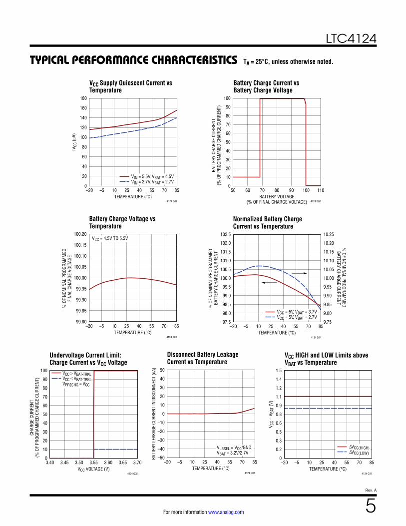
TYPICAL PERFORMANCE CHARACTERISTICS
VCC Supply Quiescent Current vs Temperature
Battery Charge Current vs Battery Charge Voltage
Battery Charge Voltage vs Temperature
Normalized Battery Charge Current vs Temperature
Undervoltage Current Limit: Charge Current vs VCC Voltage
Disconnect Battery Leakage Current vs Temperature
VCC HIGH and LOW Limits above VBAT vs Temperature
TA = 25°C, unless otherwise noted.
TEMPERATURE (°C)–20
IVCC
(µA)
180
160
120
80
40
140
100
60
20
05525
4124 G01
854010 70–5
VIN = 5.5V, VBAT = 4.5VVIN = 2.7V, VBAT = 2.7V
BATTERY VOLTAGE(% OF FINAL CHARGE VOLTAGE)
50
100
90
70
40
50
20
80
60
30
10
080
4124 G02
1109070 10060
BATT
ERY
CHAR
GE C
URRE
NT(%
OF
PROG
RAM
MED
CHA
RGE
CURR
ENT)
TEMPERATURE (°C)–20
% O
F NO
MIN
AL P
ROGR
AMM
ED
FINA
L CH
ARGE
VOL
TAGE
100.20
100.15
100.05
99.95
99.85
100.10
100.00
99.90
99.805525
4124 G03
854010 70–5
VCC = 4.5V TO 5.5V
TEMPERATURE (°C)–20
% O
F NO
MIN
AL P
ROGR
AMM
ED
BATT
ERY
CHAR
GE C
URRE
NT
102.5
102.0
101.0
100.0
98.0
101.5
100.5
99.0
99.5
98.5
97.5
% OF NOM
INAL PROGRAMM
ED BATTERY CHARGE CURRENT
10.25
10.20
10.10
10.00
9.80
10.15
10.05
9.90
9.95
9.85
9.755525
4124 G04
854010 70–5
VCC = 5V, VBAT = 3.7VVCC = 5V, VBAT = 2.7V
VCC VOLTAGE (V)3.40
100
90
70
40
50
20
80
60
30
10
03.55
4124 G05
3.703.603.50 3.653.45
CHAR
GE C
URRE
NT(%
OF
PROG
RAM
MED
CHA
RGE
CURR
ENT)
VCC > VBAT-TRKLVCC ≤ VBAT-TRKL, VPRECHG = VCC
TEMPERATURE (°C)–20
BATT
ERY
LEAK
AGE
CURR
ENT
IN D
ISCO
NNEC
T (n
A) 50
40
20
0
–40
30
10
–20
–10
–30
–505525
4124 G06
854010 70–5
VLBSEL = VCC/GND,VBAT = 3.2V/2.7V
TEMPERATURE (°C)–20
V CC
– V B
AT (V
)
1.5
1.4
1.1
0.8
0.2
1.2
0.9
0.5
0.6
0.3
05525
4124 G07
854010 70–5
∆VCC(HIGH)∆VCC(LOW)
LTC4124
6Rev. A
For more information www.analog.com
PIN FUNCTIONSVCC (Pin 1): System DC Supply. The VCC voltage range is 2.7V to 5.5V. An internal diode is connected from the ACIN pin (anode) to this pin (cathode), and a second one is connected from the DCIN pin (anode) to this pin (cath-ode). The voltage on this pin will be determined by the higher of the DCIN voltage and the peak AC voltage on the ACIN pin. There is an internal 2.2µF rectification capacitor connected between this pin and GND. Optional additional capacitance can be connected externally between this pin and GND.
CHRG (Pin 2): Charge Status Indicator. This pin is an open drain output with a 300µA current source pull down. In a typical application, this pin is pulled up by an LED to VCC. This pin has four possible states shown in Table 1.
Table 1. CHRG StatesCHRG Status
High Impedance No Input Power
Blink Slow (0.8Hz)
Powered On and Charging
Blink Fast (6Hz)
Charging Paused due to Battery Temperature Out of Range, or
Charging Stopped due to Bad Battery Detected, or
Limited Charging due to Undervoltage Current Limit
Pull Down End of Charge C/10 Reached or Charging Complete
PRECHG (Pin 3): Precharge Enable. Tie this pin to VCC to enable low current precharge at battery voltages below the precharge battery threshold (VBAT_TRKL). Tie this pin to GND to disable low current precharge. When low current precharge is disabled, full charge current will be delivered for battery voltages below the final charge volt-age. Do not leave this pin open.
VSEL1 (Pin 4): Charge Voltage Select Bit 1. Tie this pin to VCC or GND to program the battery charge voltage. Do not leave this pin open. Refer to Table 2 for programming the desired charge voltage.
VSEL2 (Pin 5): Charge Voltage Select Bit 2. Tie this pin to VCC or GND to program the battery charge voltage. Do not leave this pin open. Refer to Table 2 for programming the desired charge voltage.
Table 2. Battery Charge Voltage ProgrammingVSEL1 VSEL2 Charge Voltage
High High 4.35V
High Low 4.20V
Low High 4.10V
Low Low 4.00V
TYPICAL PERFORMANCE CHARACTERISTICS TA = 25°C, unless otherwise noted.
CHRG Pull-Down Current vs Temperature
Charge Termination Period and Bad Battery Detection Period vs Temperature
TEMPERATURE (°C)–20
I CHR
G (µ
A)
400
300
340
300
220
360
320
260
280
240
2005525
4124 G08
854010 70–5
VCHRG = 0.4V
TEMPERATURE (°C)–20
CHAR
GE T
ERM
INAT
ION
PERI
OD (H
OURS
)
3.8
3.6
3.2
2.8
3.4
3.0
2.4
2.6
2.2
BAD BATTERY DETECTION PERIOD (MINS)
61
57
49
41
53
45
37
33
295525
4124 G09
854010 70–5
CHARGE TERMINATION PERIODBAD BATTERY DETECTION PERIOD
VCC = 5V
LTC4124
7Rev. A
For more information www.analog.com
PIN FUNCTIONSISEL1 (Pin 6): Charge Current Select Bit 1. Tie this pin to VCC or GND to program the battery charge current. Do not leave this pin open. Refer to Table 3 for programming the desired charge current.
ISEL2 (Pin 7): Charge Current Select Bit 2. Tie this pin to VCC or GND to program the battery charge current. Do not leave this pin open. Refer to Table 3 for programming the desired charge current.
Table 3. Battery Charge Current ProgrammingISEL1 ISEL2 Charge Current
High High 100mA
High Low 50mA
Low High 25mA
Low Low 10mA
LBSEL (Pin 8): Low Battery Disconnect Voltage Select. Tie this pin to VCC or GND to program the low battery disconnect voltage level. Do not leave this pin open. Refer to Table 4 for programming the desired low battery dis-connect voltage level.
Table 4. Low Battery Disconnect Voltage ProgrammingLBSEL Disconnect Voltage
High 3.2V
Low 2.7V
NTC (Pin 9): Thermistor Input. Connect a 100kΩ thermis-tor from NTC to GND. This pin is internally pulled up with a 100kΩ, 1% resistor to VCC. The voltage level on this pin determines if the battery temperature is safe for charging. Charging and the charge timer are paused if the thermis-tor indicates temperature that is unsafe for charging. Once the temperature returns to the safe region, charging and the charge timer resume. Connect this pin to VCC to dis-able the temperature qualified charging feature.
BAT (Pin 10): Battery. Connect the Li-Ion battery to this pin.
ACIN (Pin 11): AC Input Supply Voltage. Connect the external LC tank (receive inductor and capacitor) to this pin. An internal diode is connected from this pin (anode) to the VCC pin (cathode). This pin supplies power to the VCC pin when its peak voltage is higher than the DCIN pin voltage. Short this pin to GND when not used.
DCIN (Pin 12): Optional DC Input Supply Voltage: 3.3V to 5.5V. An internal diode is connected from this pin (anode) to the VCC pin (cathode). This pin supplies power to the VCC pin when its voltage is higher than the peak voltage of the ACIN pin. Short this pin to GND when not used.
GND (Exposed Pad, Pin 13): Device Ground. Connect this ground pin to a suitable PCB copper ground plane for proper electrical operation and rated thermal performance.
LTC4124
8Rev. A
For more information www.analog.com
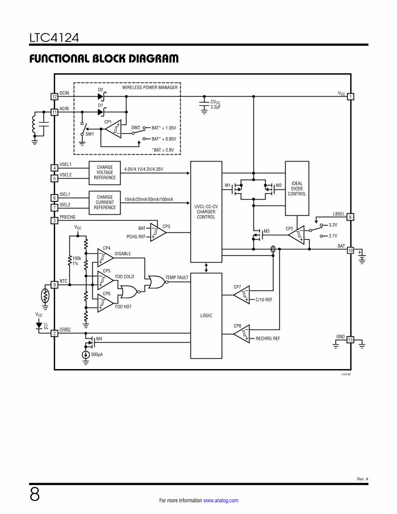
FUNCTIONAL BLOCK DIAGRAM
4124 BD
+
+–
+–
+–
+–
+–
+–
+–
+–
DISABLE
CP3
CP4
CP5
CP2
CP6
TEMP FAULT
100k1%
TOO COLD
TOO HOT
CP7
CP8
BAT
PCHG REF
3.2V
2.7V
M1 M2
M3
C/10 REF
RECHRG REF
IDEALDIODE
CONTROL
CHARGEVOLTAGE
REFERENCE
CHARGECURRENT
REFERENCE UVCL-CC-CVCHARGERCONTROL
LOGIC
4.0V/4.1V/4.2V/4.35V
WIRELESS POWER MANAGER
10mA/25mA/50mA/100mA
CP1BAT* + 1.05V
BAT* + 0.85V
*BAT ≥ 2.8V
CVCC2.2µF
VCC
SW2SW1
7ISEL2
6ISEL1
5VSEL2
4VSEL1
11ACIN
12 1DCIN VCC
D2
D1
13
9
3
2
NTC
PRECHG
CHRG
BAT
8
10
LBSEL
GNDM4
300µA
VCC
LTC4124
9Rev. A
For more information www.analog.com
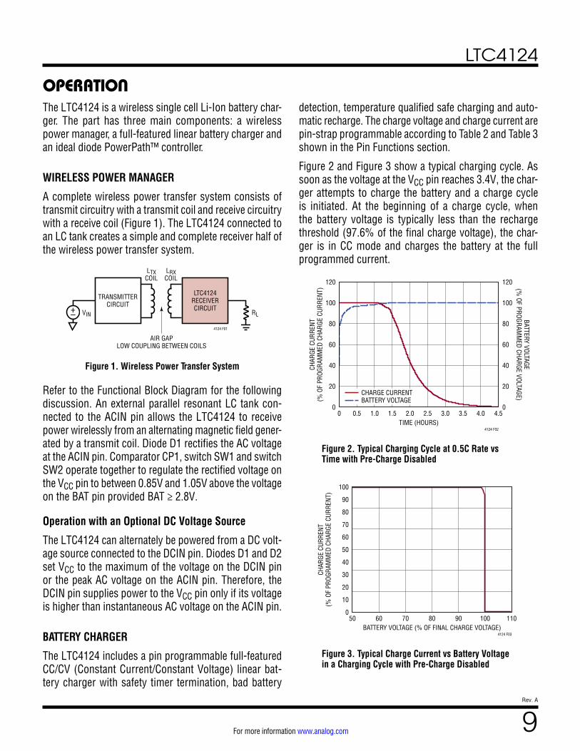
OPERATIONThe LTC4124 is a wireless single cell Li-Ion battery char-ger. The part has three main components: a wireless power manager, a full-featured linear battery charger and an ideal diode PowerPath™ controller.
WIRELESS POWER MANAGER
A complete wireless power transfer system consists of transmit circuitry with a transmit coil and receive circuitry with a receive coil (Figure 1). The LTC4124 connected to an LC tank creates a simple and complete receiver half of the wireless power transfer system.
Figure 1.
+–
LTC4124RECEIVERCIRCUIT
TRANSMITTERCIRCUIT
4124 F01
VIN RL
LRXCOIL
LTXCOIL
AIR GAPLOW COUPLING BETWEEN COILS
Wireless Power Transfer System
Refer to the Functional Block Diagram for the following discussion. An external parallel resonant LC tank con-nected to the ACIN pin allows the LTC4124 to receive power wirelessly from an alternating magnetic field gener-ated by a transmit coil. Diode D1 rectifies the AC voltage at the ACIN pin. Comparator CP1, switch SW1 and switch SW2 operate together to regulate the rectified voltage on the VCC pin to between 0.85V and 1.05V above the voltage on the BAT pin provided BAT ≥ 2.8V.
Operation with an Optional DC Voltage Source
The LTC4124 can alternately be powered from a DC volt-age source connected to the DCIN pin. Diodes D1 and D2 set VCC to the maximum of the voltage on the DCIN pin or the peak AC voltage on the ACIN pin. Therefore, the DCIN pin supplies power to the VCC pin only if its voltage is higher than instantaneous AC voltage on the ACIN pin.
BATTERY CHARGER
The LTC4124 includes a pin programmable full-featured CC/CV (Constant Current/Constant Voltage) linear bat-tery charger with safety timer termination, bad battery
detection, temperature qualified safe charging and auto-matic recharge. The charge voltage and charge current are pin-strap programmable according to Table 2 and Table 3 shown in the Pin Functions section.
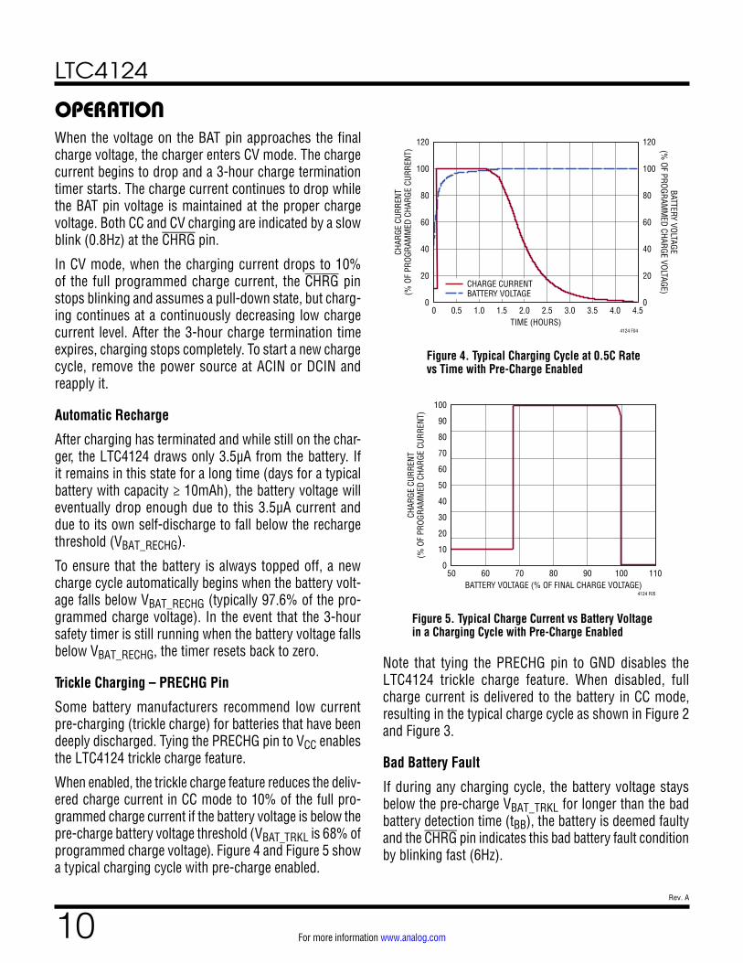
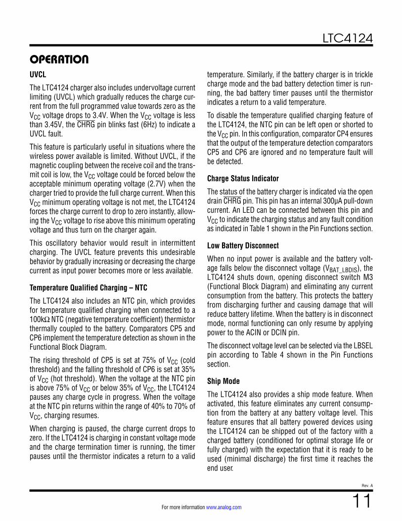
Figure 2 and Figure 3 show a typical charging cycle. As soon as the voltage at the VCC pin reaches 3.4V, the char-ger attempts to charge the battery and a charge cycle is initiated. At the beginning of a charge cycle, when the battery voltage is typically less than the recharge threshold (97.6% of the final charge voltage), the char-ger is in CC mode and charges the battery at the full programmed current.
Figure 2.
TIME (HOURS)0
CHAR
GE C
URRE
NT(%
OF
PROG
RAM
MED
CHA
RGE
CURR
ENT)
120
100
60
20
80
40
0
BATTERY VOLTAGE(%
OF PROGRAMM
ED CHARGE VOLTAGE)
120
100
60
20
80
40
02.51.5 3.5
4124 F02
4.0 4.52.01.0 3.00.5
CHARGE CURRENTBATTERY VOLTAGE
Typical Charging Cycle at 0.5C Rate vs Time with Pre-Charge Disabled
Figure 3.
BATTERY VOLTAGE (% OF FINAL CHARGE VOLTAGE)50
CHAR
GE C
URRE
NT(%
OF
PROG
RAM
MED
CHA
RGE
CURR
ENT)
100
90
60
20
80
40
0
70
30
50
10
10080
4124 F03
110907060
Typical Charge Current vs Battery Voltage in a Charging Cycle with Pre-Charge Disabled
LTC4124
10Rev. A
For more information www.analog.com
OPERATIONWhen the voltage on the BAT pin approaches the final charge voltage, the charger enters CV mode. The charge current begins to drop and a 3-hour charge termination timer starts. The charge current continues to drop while the BAT pin voltage is maintained at the proper charge voltage. Both CC and CV charging are indicated by a slow blink (0.8Hz) at the CHRG pin.
In CV mode, when the charging current drops to 10% of the full programmed charge current, the CHRG pin stops blinking and assumes a pull-down state, but charg-ing continues at a continuously decreasing low charge current level. After the 3-hour charge termination time expires, charging stops completely. To start a new charge cycle, remove the power source at ACIN or DCIN and reapply it.
Automatic Recharge
After charging has terminated and while still on the char-ger, the LTC4124 draws only 3.5µA from the battery. If it remains in this state for a long time (days for a typical battery with capacity ≥ 10mAh), the battery voltage will eventually drop enough due to this 3.5µA current and due to its own self-discharge to fall below the recharge threshold (VBAT_RECHG).
To ensure that the battery is always topped off, a new charge cycle automatically begins when the battery volt-age falls below VBAT_RECHG (typically 97.6% of the pro-grammed charge voltage). In the event that the 3-hour safety timer is still running when the battery voltage falls below VBAT_RECHG, the timer resets back to zero.
Trickle Charging – PRECHG Pin
Some battery manufacturers recommend low current pre-charging (trickle charge) for batteries that have been deeply discharged. Tying the PRECHG pin to VCC enables the LTC4124 trickle charge feature.
When enabled, the trickle charge feature reduces the deliv-ered charge current in CC mode to 10% of the full pro-grammed charge current if the battery voltage is below the pre-charge battery voltage threshold (VBAT_TRKL is 68% of programmed charge voltage). Figure 4 and Figure 5 show a typical charging cycle with pre-charge enabled.
Figure 4.
TIME (HOURS)0
CHAR
GE C
URRE
NT(%
OF
PROG
RAM
MED
CHA
RGE
CURR
ENT)
120
100
60
20
80
40
02.51.5 3.5
4124 F04
4.0 4.52.01.0 3.00.5
BATTERY VOLTAGE(%
OF PROGRAMM
ED CHARGE VOLTAGE)
120
100
60
20
80
40
0
CHARGE CURRENTBATTERY VOLTAGE
Typical Charging Cycle at 0.5C Rate vs Time with Pre-Charge Enabled
Figure 5.
BATTERY VOLTAGE (% OF FINAL CHARGE VOLTAGE)50
CHAR
GE C
URRE
NT(%
OF
PROG
RAM
MED
CHA
RGE
CURR
ENT)
100
90
60
20
80
40
0
70
30
50
10
10080
4124 F05
110907060
Typical Charge Current vs Battery Voltage in a Charging Cycle with Pre-Charge Enabled
Note that tying the PRECHG pin to GND disables the LTC4124 trickle charge feature. When disabled, full charge current is delivered to the battery in CC mode, resulting in the typical charge cycle as shown in Figure 2 and Figure 3.
Bad Battery Fault
If during any charging cycle, the battery voltage stays below the pre-charge VBAT_TRKL for longer than the bad battery detection time (tBB), the battery is deemed faulty and the CHRG pin indicates this bad battery fault condition by blinking fast (6Hz).
LTC4124
11Rev. A
For more information www.analog.com
OPERATIONUVCL
The LTC4124 charger also includes undervoltage current limiting (UVCL) which gradually reduces the charge cur-rent from the full programmed value towards zero as the VCC voltage drops to 3.4V. When the VCC voltage is less than 3.45V, the CHRG pin blinks fast (6Hz) to indicate a UVCL fault.
This feature is particularly useful in situations where the wireless power available is limited. Without UVCL, if the magnetic coupling between the receive coil and the trans-mit coil is low, the VCC voltage could be forced below the acceptable minimum operating voltage (2.7V) when the charger tried to provide the full charge current. When this VCC minimum operating voltage is not met, the LTC4124 forces the charge current to drop to zero instantly, allow-ing the VCC voltage to rise above this minimum operating voltage and thus turn on the charger again.
This oscillatory behavior would result in intermittent charging. The UVCL feature prevents this undesirable behavior by gradually increasing or decreasing the charge current as input power becomes more or less available.
Temperature Qualified Charging – NTC
The LTC4124 also includes an NTC pin, which provides for temperature qualified charging when connected to a 100kΩ NTC (negative temperature coefficient) thermistor thermally coupled to the battery. Comparators CP5 and CP6 implement the temperature detection as shown in the Functional Block Diagram.
The rising threshold of CP5 is set at 75% of VCC (cold threshold) and the falling threshold of CP6 is set at 35% of VCC (hot threshold). When the voltage at the NTC pin is above 75% of VCC or below 35% of VCC, the LTC4124 pauses any charge cycle in progress. When the voltage at the NTC pin returns within the range of 40% to 70% of VCC, charging resumes.
When charging is paused, the charge current drops to zero. If the LTC4124 is charging in constant voltage mode and the charge termination timer is running, the timer pauses until the thermistor indicates a return to a valid
temperature. Similarly, if the battery charger is in trickle charge mode and the bad battery detection timer is run-ning, the bad battery timer pauses until the thermistor indicates a return to a valid temperature.
To disable the temperature qualified charging feature of the LTC4124, the NTC pin can be left open or shorted to the VCC pin. In this configuration, comparator CP4 ensures that the output of the temperature detection comparators CP5 and CP6 are ignored and no temperature fault will be detected.
Charge Status Indicator
The status of the battery charger is indicated via the open drain CHRG pin. This pin has an internal 300µA pull-down current. An LED can be connected between this pin and VCC to indicate the charging status and any fault condition as indicated in Table 1 shown in the Pin Functions section.
Low Battery Disconnect
When no input power is available and the battery volt-age falls below the disconnect voltage (VBAT_LBDIS), the LTC4124 shuts down, opening disconnect switch M3 (Functional Block Diagram) and eliminating any current consumption from the battery. This protects the battery from discharging further and causing damage that will reduce battery lifetime. When the battery is in disconnect mode, normal functioning can only resume by applying power to the ACIN or DCIN pin.
The disconnect voltage level can be selected via the LBSEL pin according to Table 4 shown in the Pin Functions section.
Ship Mode
The LTC4124 also provides a ship mode feature. When activated, this feature eliminates any current consump-tion from the battery at any battery voltage level. This feature ensures that all battery powered devices using the LTC4124 can be shipped out of the factory with a charged battery (conditioned for optimal storage life or fully charged) with the expectation that it is ready to be used (minimal discharge) the first time it reaches the end user.
LTC4124
12Rev. A
For more information www.analog.com
OPERATIONShip mode activates when a 1.5V (± 100mV) DC voltage is simultaneously applied to both the DCIN and the ACIN pins while the LTC4124 is in ideal diode mode (the bat-tery is supporting the VCC voltage at or above the battery disconnect voltage VBAT_LBDIS).
Before entering ship mode, the voltage at VCC will be at VBAT – 50mV. As soon as 1.5V is simultaneously applied to the DCIN and ACIN pins, the voltage at VCC will drop to a diode drop below 1.5V (approximately 0.7V), indicating that the part is now in ship mode. Finally, set the DCIN and ACIN pins to 0V to let the VCC pin voltage drop to 0V.
In a typical setup, an RX coil is connected between the ACIN pin and GND. Thus, driving the ACIN pin with a 1.5V DC voltage is not prudent without temporarily removing this coil connection. An alternate and more practical pro-cedure for entering ship mode is as follows:
1. With DCIN = 0V, ensure that the LTC4124 is in ideal diode mode (the battery is supporting the VCC voltage at or above the battery disconnect voltage VBAT_LBDIS).
2. Turn on the transmitter and couple the TX coil to the RX coil so that the LTC4124 is in charging mode (VCC is supported by ACIN at or above the battery voltage).
3. Drive the DCIN pin to 1.5V DC.
4. Turn off the transmitter.
5. Ensure that the VCC voltage drops to a diode drop below 1.5V (approximately 0.7V).
6. Remove the 1.5V DC source from the DCIN pin and drive it to 0V.
7. Ensure that the VCC voltage goes to 0V.
Once in ship mode, normal functioning of the LTC4124 can only resume again by applying power to the ACIN or DCIN pin to bring the voltage at VCC above the 2.7V minimum operating voltage.
IDEAL DIODE POWER PATH FROM BAT TO VCC
When the LTC4124 is not in low battery disconnect mode nor in ship mode, the Ideal Diode Control block (Functional Block Diagram) regulates VCC to achieve low loss conduction by driving the gate of M2 such that the voltage drop from the BAT pin to the VCC pin is 50mV. At high load currents from VCC, M2 is fully driven on with its on-resistance adding to that of M3 connecting BAT to VCC.
The Charger Control block driving M1 together with the Ideal Diode Control block driving M2 allow for a smooth transition from charging mode to the low loss discharge mode. Note that in charging mode, current is flowing from the VCC pin to the BAT pin. In the low loss discharge (ideal diode) mode, current is flowing from the BAT pin to sup-port the VCC pin voltage to be as close to that of the BAT pin as possible.
LTC4124
13Rev. A
For more information www.analog.com
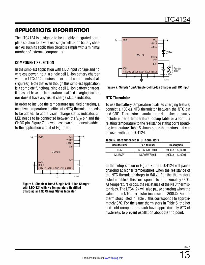
APPLICATIONS INFORMATIONThe LTC4124 is designed to be a highly integrated com-plete solution for a wireless single cell Li-Ion battery char-ger. As such its application circuit is simple with a minimal number of external components.
COMPONENT SELECTION
In the simplest application with a DC input voltage and no wireless power input, a single cell Li-Ion battery charger with the LTC4124 requires no external components at all (Figure 6). Note that even though this simplest application is a complete functional single cell Li-Ion battery charger, it does not have the temperature qualified charging feature nor does it have any visual charge status indicator.
In order to include the temperature qualified charging, a negative temperature coefficient (NTC) thermistor needs to be added. To add a visual charge status indicator, an LED needs to be connected between the VCC pin and the CHRG pin. Figure 7 shows these two components added to the application circuit of Figure 6.
Figure 6.
5V
LTC4124
4124 F06
VCCVSEL2LBSEL
NTC
DCIN
BATACINCHRGPRECHG VSEL1 GND ISEL1 ISEL2
+
Simplest 10mA Single Cell Li-Ion Charger with LTC4124 with No Temperature Qualified Charging and No Charge Status Indicator
Figure 7.
5V
RNTCRX100k
DRXLTC4124
4124 F07
VCCVSEL2LBSEL
CHRG
DCIN
NTCBAT
ACINPRECHG
+VSEL1 GND ISEL1 ISEL2
Simple 10mA Single Cell Li-Ion Charger with DC Input
NTC Thermistor
To use the battery temperature qualified charging feature, connect a 100kΩ NTC thermistor between the NTC pin and GND. Thermistor manufacturer data sheets usually include either a temperature lookup table or a formula relating temperature to the resistance at that correspond-ing temperature. Table 5 shows some thermistors that can be used with the LTC4124.
Table 5. Recommended NTC ThermistorsManufacturer Part Number Description
TDK NTCG064EF104F 100kΩ, 1%, 0201
MURATA NCP03WF104F 100kΩ, 1%, 0201
In the setup shown in Figure 7, the LTC4124 will pause charging at higher temperatures when the resistance of the NTC thermistor drops to 54kΩ. For the thermistors listed in Table 5, this corresponds to approximately 43°C. As temperature drops, the resistance of the NTC thermis-tor rises. The LTC4124 will also pause charging when the value of the NTC thermistor increases to 300kΩ. For the thermistors listed in Table 5, this corresponds to approxi-mately 3°C. For the same thermistors in Table 5, the hot and cold comparators each have approximately 5°C of hysteresis to prevent oscillation about the trip point.
LTC4124
14Rev. A
For more information www.analog.com
APPLICATIONS INFORMATIONLED
The LED connected to the CHRG pin is powered by a 300µA pull-down current source. Select a high efficiency LED with a low forward voltage drop. Some recommended LEDs are shown in Table 6.
Table 6. Recommended LEDsManufacturer Part Number Description
Kingbright APG0603VGC Green, 0201
Kingbright APG0603SEC-E-TT Red, 0201
Wireless Power Components
In order for the LTC4124 to receive power wirelessly, a parallel LC tank needs to be connected to the ACIN pin as shown in the Functional Block Diagram. The inductor L acts as the receive coil, and together with the capacitance C, creates a resonant tank circuit. Power transmission across the weakly coupled link between the transmit coil and the receive coil (Figure 1) can be greatly improved when this tank circuit is tuned to the same frequency as the transmit coil AC current frequency.
Receive Coil/Resonant Inductor L
The most important factor in selecting the receive coil is the quality factor of the coil:
QL =
ωnLRS
where ωn is the operating resonant frequency in rad/s and RS is the parasitic series resistance of the coil. Often this quality factor is limited by the size of the application. The smaller the size of the application, the harder it is to fit wire with small series resistance to generate higher inductance values. Therefore, in many cases, users are recommended to first consider the overall size of their end application and then decide on the biggest possible coil that fits this end application device.
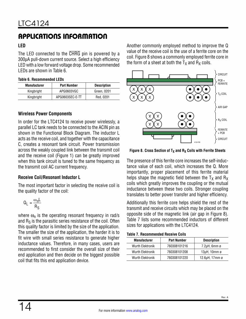
Another commonly employed method to improve the Q value of the receive coil is the use of a ferrite core on the coil. Figure 8 shows a commonly employed ferrite core in the form of a sheet at both the TX and RX coils.
Figure 8.
4124 F08
PCB + FERRITE
CIRCUIT
TX COIL
FERRITE + PCB
CIRCUIT
AIR GAP
RX COIL
Cross Section of TX and RX Coils with Ferrite Sheets
The presence of this ferrite core increases the self-induc-tance value of each coil, which increases the Q. More importantly, proper placement of this ferrite material helps shape the magnetic field between the TX and RX coils which greatly improves the coupling or the mutual inductance between these two coils. Stronger coupling translates to better power transfer and higher efficiency.
Additionally this ferrite core helps shield the rest of the transmit and receive circuits which may be placed on the opposite side of the magnetic link (air gap in Figure 8). Table 7 lists some recommended inductors of different sizes for applications with the LTC4124.
Table 7. Recommended Receive CoilsManufacturer Part Number Description
Wurth Elektronik 760308101216 7.2µH, 6mm ø
Wurth Elektronik 760308101208 13µH, 10mm ø
Wurth Elektronik 760308101220 12.6µH, 17mm ø
LTC4124
15Rev. A
For more information www.analog.com
APPLICATIONS INFORMATIONResonant Frequency Selection
As noted in the quality factor discussion of the receive coil, the higher the frequency of operation, the higher the quality factor of the coil. However, there are several limita-tions to setting the operating frequency to an arbitrarily high value.
The first is the self-resonant frequency of the coil. For the coils listed in Table 7, their self-resonant frequencies vary from 19MHz to 32MHz. The operating frequency should be set at least a factor of 5 below the coil self-resonant frequency so that this operating frequency can be well controlled by selecting the appropriate resonant capaci-tor value.
The second limitation is the transmitter circuit driver capability and efficiency. In most wireless power appli-cations, the transmit circuit includes a DC to AC converter. The higher the operating frequency, the faster some ele-ments of the transmit circuit need to switch. The speed at which these elements can be switched is often limited due to the architecture or process technology. Furthermore, a higher switching frequency lends itself to higher switch-ing losses, which in turn reduces overall efficiency.
Therefore, as a guideline, the user should select a high operating frequency that is appropriate for the selected coils and transmitter circuit driver. The main trade-off is between the loss in efficiency of the transmitter circuit driver operating at higher frequency and the increase in coil to coil power transfer due to the higher Q of the coils. The LTC4124 is appropriate for systems with resonant frequencies anywhere from 50kHz up to 10MHz.
Resonant Capacitor C
Once the coil and the operating frequency are selected, the value of the resonant capacitor is determined by the following formula:
C =
1
ωn2L
where ωn is the operating resonant frequency in rad/s and L is the receive coil inductance. Select capacitors with low ESR and low thermal coefficients such as COG or X7R
ceramic. In general, the higher the voltage rating of the capacitor, the lower the dissipation factor of its dielectric material but also the larger the size would be. The dissipa-tion factor of a capacitor includes the ESR as one of its main components. Note that this dissipation factor is not usually listed in a standard capacitor data sheet.
Table 8 lists some recommended capacitors of different sizes for applications with the LTC4124.
Table 8. Recommended Resonant CapacitorsManufacturer Part Number Description
Murata GRM155R71H332JA01D 50V, 0402, 3.3nF
Murata GRM155R71H683KE14J 50V, 0402, 68nF
Murata GRM155R71H333KE14D 50V, 0402, 33nF
TDK CGA4J2C0G1H333J125AA 50V, 0805, 33nF
Choosing Transmit Power Level
The transmit power level should be set as low as possible for the receiver to receive the desired output power under the worst-case coupling conditions (i.e. maximum trans-mit distance with the worst-case alignment). Although the LTC4124 is capable of shunting excess received power to maintain the VCC voltage in the desired range, its tempera-ture will rise when shunting excess power. Careful evalu-ation of the application needs to be performed to ensure that the operating temperature range of the LTC4124 and the end application is not exceeded.
Empirically, the determination of transmit power level of the application circuit can be done by first setting the transmit inductor current at the highest rated current pos-sible based on the transmit coil specification. From this starting point, transmit power can then be adjusted lower until the charge current of the LTC4124 on the receive side is negatively impacted under worst-case coupling condi-tions. Once this minimum transmit power level is deter-mined, the transmit and receive coils should be arranged under best-case coupling conditions with a fully charged battery to make sure that the shunting of excess power by the LTC4124 does not raise its temperature too much.
In addition to temperature, another parameter that needs to be checked is the maximum negative voltage on the
LTC4124
16Rev. A
For more information www.analog.com
APPLICATIONS INFORMATIONACIN pin. Following the procedure above, when evaluating the rise in temperature of the LTC4124 under the best-case coupling conditions, ensure that VVCC – VACIN does not exceed 40V. Figure 9 shows a typical waveform on ACIN showing VCC – VACIN < 40V.
Figure 9.
TIME (µs)0
V ACI
N (V
)
8
-12
4
6
0
–4
–8
2
–2
–6
–10
–1415 355 25
4124 F09
4010 3020
VCC = 5.5V
Typical Acceptable Voltage Waveform on the ACIN pin with VCC – VACIN < 40V.
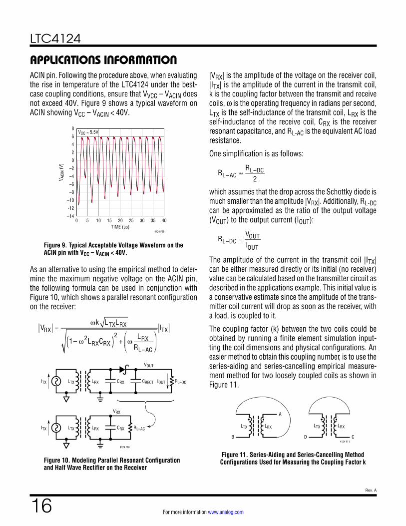
As an alternative to using the empirical method to deter-mine the maximum negative voltage on the ACIN pin, the following formula can be used in conjunction with Figure 10, which shows a parallel resonant configuration on the receiver:
VRX =ωk LTXLRX
1– ω2LRXCRX( )2
+ ωLRX
RL–AC
⎛
⎝⎜
⎞
⎠⎟
ITX
Figure 10.
4124 F10
LRX CRX RL–ACLTXITX
VRX
LRX CRX CRECT RL–DCLTXITX IOUT
VOUT
Modeling Parallel Resonant Configuration and Half Wave Rectifier on the Receiver
|VRX| is the amplitude of the voltage on the receiver coil, |ITX| is the amplitude of the current in the transmit coil, k is the coupling factor between the transmit and receive coils, ω is the operating frequency in radians per second, LTX is the self-inductance of the transmit coil, LRX is the self-inductance of the receive coil, CRX is the receiver resonant capacitance, and RL-AC is the equivalent AC load resistance.
One simplification is as follows:
RL–AC ≈
RL–DC2
which assumes that the drop across the Schottky diode is much smaller than the amplitude |VRX|. Additionally, RL-DC can be approximated as the ratio of the output voltage (VOUT) to the output current (IOUT):
RL–DC =
VOUTIOUT
The amplitude of the current in the transmit coil |ITX| can be either measured directly or its initial (no receiver) value can be calculated based on the transmitter circuit as described in the applications example. This initial value is a conservative estimate since the amplitude of the trans-mitter coil current will drop as soon as the receiver, with a load, is coupled to it.
The coupling factor (k) between the two coils could be obtained by running a finite element simulation input-ting the coil dimensions and physical configurations. An easier method to obtain this coupling number, is to use the series-aiding and series-cancelling empirical measure-ment method for two loosely coupled coils as shown in Figure 11.
Figure 11.
•• • •
4124 F11
LTXLTX LRXLRX
A
B CD
Series-Aiding and Series-Cancelling Method Configurations Used for Measuring the Coupling Factor k
LTC4124
17Rev. A
For more information www.analog.com
APPLICATIONS INFORMATIONAnd:
LAIDING = LAB
LCANCELLING = LCD
k =LAIDING – LCANCELLING
4 LTXLRX
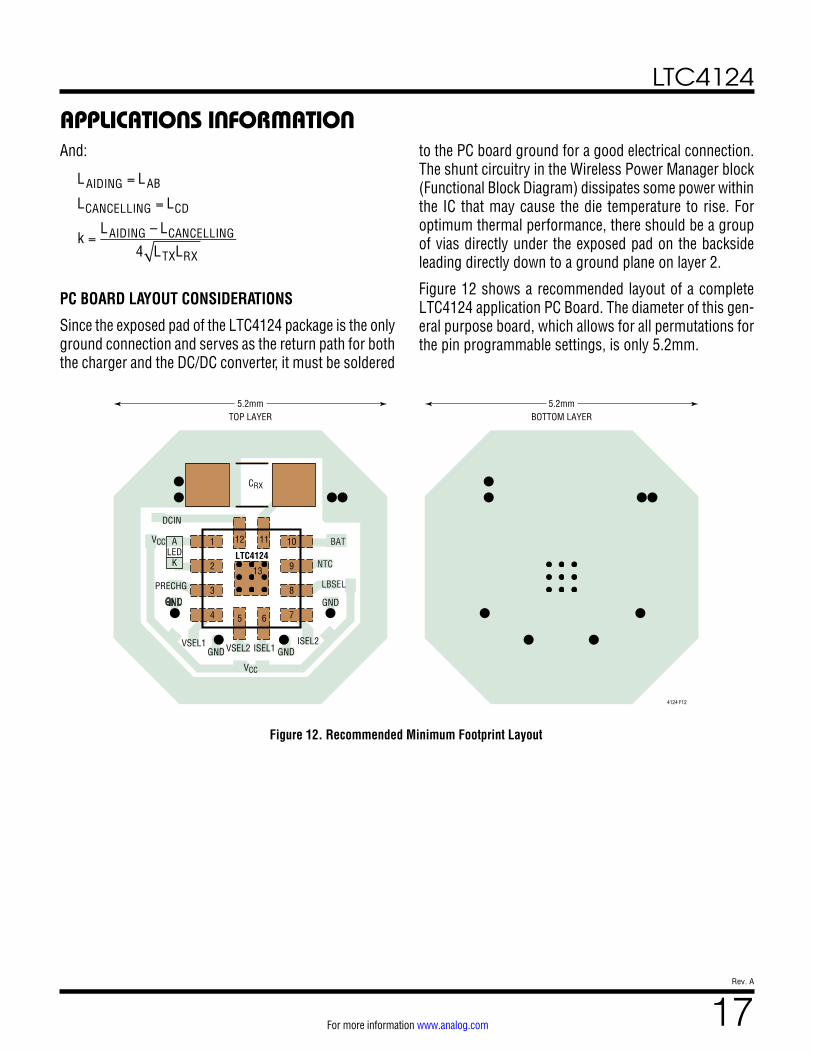
PC BOARD LAYOUT CONSIDERATIONS
Since the exposed pad of the LTC4124 package is the only ground connection and serves as the return path for both the charger and the DC/DC converter, it must be soldered
to the PC board ground for a good electrical connection. The shunt circuitry in the Wireless Power Manager block (Functional Block Diagram) dissipates some power within the IC that may cause the die temperature to rise. For optimum thermal performance, there should be a group of vias directly under the exposed pad on the backside leading directly down to a ground plane on layer 2.
Figure 12 shows a recommended layout of a complete LTC4124 application PC Board. The diameter of this gen-eral purpose board, which allows for all permutations for the pin programmable settings, is only 5.2mm.
Figure 12.
VCC
CRX
VCC
BAT
NTC
DCIN
ISEL1ISEL2
VSEL2
10
9
8
7
1
2
3
4
13
12 11
5 6
LTC4124
GND
GNDGNDVSEL1
PRECHG LBSEL
4124 F12
BOTTOM LAYERTOP LAYER5.2mm5.2mm
ALED
K
Recommended Minimum Footprint Layout
LTC4124
18Rev. A
For more information www.analog.com
APPLICATIONS INFORMATION
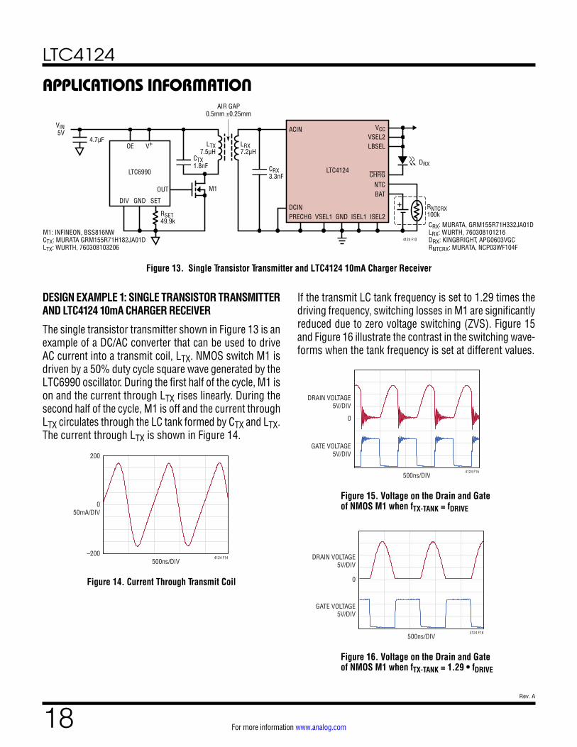
DESIGN EXAMPLE 1: SINGLE TRANSISTOR TRANSMITTER AND LTC4124 10mA CHARGER RECEIVER
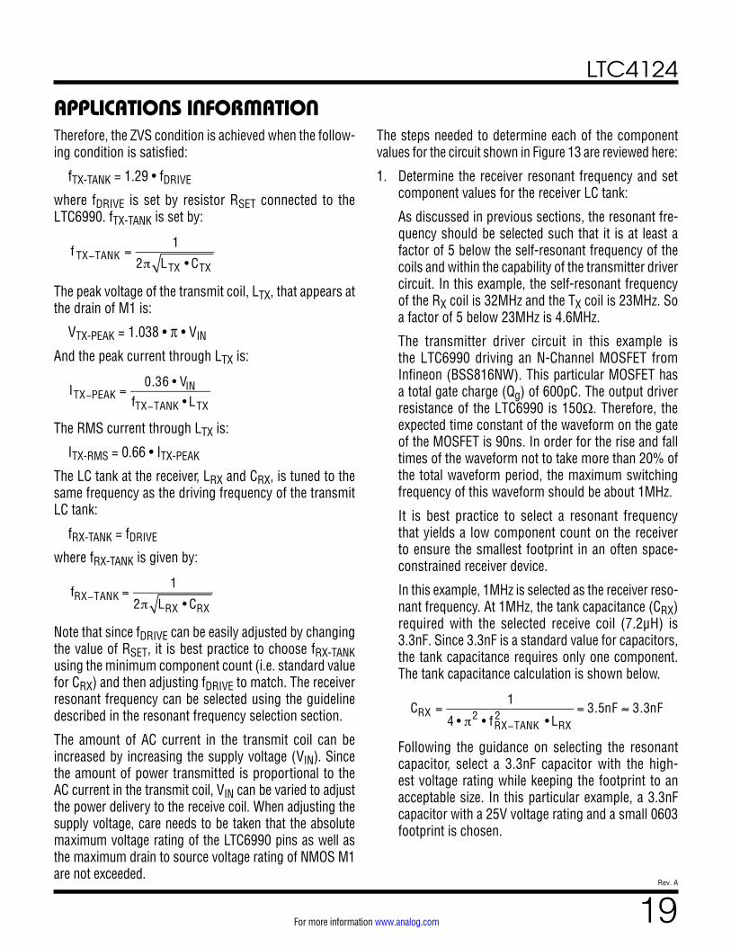
The single transistor transmitter shown in Figure 13 is an example of a DC/AC converter that can be used to drive AC current into a transmit coil, LTX. NMOS switch M1 is driven by a 50% duty cycle square wave generated by the LTC6990 oscillator. During the first half of the cycle, M1 is on and the current through LTX rises linearly. During the second half of the cycle, M1 is off and the current through LTX circulates through the LC tank formed by CTX and LTX. The current through LTX is shown in Figure 14.
Figure 14.
500ns/DIV
200
50mA/DIV0
–2004124 F14
Current Through Transmit Coil
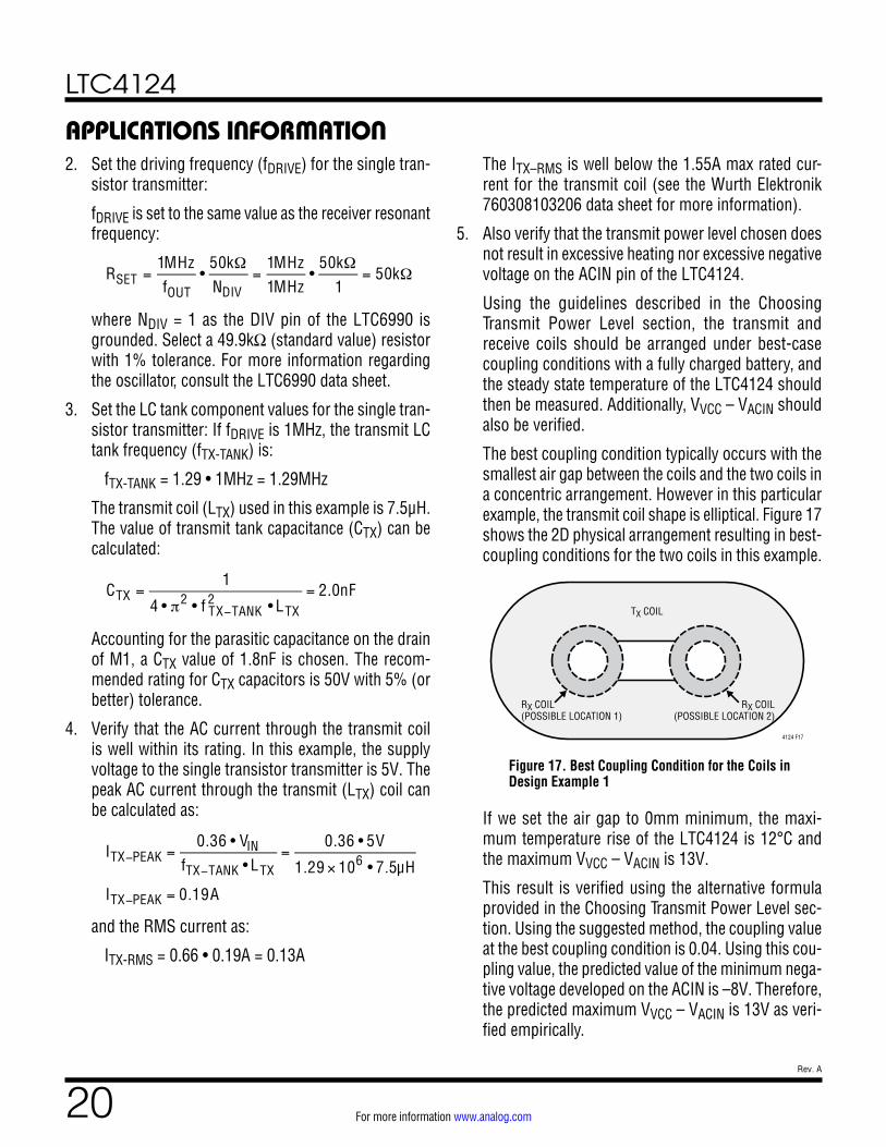
If the transmit LC tank frequency is set to 1.29 times the driving frequency, switching losses in M1 are significantly reduced due to zero voltage switching (ZVS). Figure 15 and Figure 16 illustrate the contrast in the switching wave-forms when the tank frequency is set at different values.
Figure 15.
500ns/DIV
DRAIN VOLTAGE5V/DIV
GATE VOLTAGE5V/DIV
0
4124 F15
Voltage on the Drain and Gate of NMOS M1 when fTX-TANK = fDRIVE
Figure 16.
500ns/DIV
DRAIN VOLTAGE5V/DIV
GATE VOLTAGE5V/DIV
0
4124 F16
Voltage on the Drain and Gate of NMOS M1 when fTX-TANK = 1.29 • fDRIVE
Figure 13.
RNTCRX100kRSET
49.9k
LTC4124
4124 F13
VCCVSEL2LBSEL
CHRG
ACIN
NTCBAT
DCINPRECHG
+VSEL1 GND ISEL1
DIV GND SET
OUT
ISEL2
LRX7.2µH
DRXLTC6990
M1: INFINEON, BSS816NWCTX: MURATA GRM155R71H182JA01D LTX: WURTH, 760308103206
CRX: MURATA, GRM155R71H332JA01D LRX: WURTH, 760308101216 DRX: KINGBRIGHT, APG0603VGCRNTCRX: MURATA, NCP03WF104F
M1
VIN5V
LTX7.5µH
CTX1.8nF CRX
3.3nF
4.7µFV+OE
AIR GAP0.5mm ±0.25mm
Single Transistor Transmitter and LTC4124 10mA Charger Receiver
LTC4124
19Rev. A
For more information www.analog.com
APPLICATIONS INFORMATIONTherefore, the ZVS condition is achieved when the follow-ing condition is satisfied:
fTX-TANK = 1.29 • fDRIVE
where fDRIVE is set by resistor RSET connected to the LTC6990. fTX-TANK is set by:
f TX−TANK =
1
2π LTX • CTX
The peak voltage of the transmit coil, LTX, that appears at the drain of M1 is:
VTX-PEAK = 1.038 • π • VIN
And the peak current through LTX is:
ITX−PEAK =
0.36 • VINfTX−TANK • LTX
The RMS current through LTX is:
ITX-RMS = 0.66 • ITX-PEAK
The LC tank at the receiver, LRX and CRX, is tuned to the same frequency as the driving frequency of the transmit LC tank:
fRX-TANK = fDRIVE
where fRX-TANK is given by:
fRX−TANK =
1
2π LRX • CRX
Note that since fDRIVE can be easily adjusted by changing the value of RSET, it is best practice to choose fRX-TANK using the minimum component count (i.e. standard value for CRX) and then adjusting fDRIVE to match. The receiver resonant frequency can be selected using the guideline described in the resonant frequency selection section.
The amount of AC current in the transmit coil can be increased by increasing the supply voltage (VIN). Since the amount of power transmitted is proportional to the AC current in the transmit coil, VIN can be varied to adjust the power delivery to the receive coil. When adjusting the supply voltage, care needs to be taken that the absolute maximum voltage rating of the LTC6990 pins as well as the maximum drain to source voltage rating of NMOS M1 are not exceeded.
The steps needed to determine each of the component values for the circuit shown in Figure 13 are reviewed here:
1. Determine the receiver resonant frequency and set component values for the receiver LC tank:
As discussed in previous sections, the resonant fre-quency should be selected such that it is at least a factor of 5 below the self-resonant frequency of the coils and within the capability of the transmitter driver circuit. In this example, the self-resonant frequency of the RX coil is 32MHz and the TX coil is 23MHz. So a factor of 5 below 23MHz is 4.6MHz.
The transmitter driver circuit in this example is the LTC6990 driving an N-Channel MOSFET from Infineon (BSS816NW). This particular MOSFET has a total gate charge (Qg) of 600pC. The output driver resistance of the LTC6990 is 150Ω. Therefore, the expected time constant of the waveform on the gate of the MOSFET is 90ns. In order for the rise and fall times of the waveform not to take more than 20% of the total waveform period, the maximum switching frequency of this waveform should be about 1MHz.
It is best practice to select a resonant frequency that yields a low component count on the receiver to ensure the smallest footprint in an often space-constrained receiver device.
In this example, 1MHz is selected as the receiver reso-nant frequency. At 1MHz, the tank capacitance (CRX) required with the selected receive coil (7.2μH) is 3.3nF. Since 3.3nF is a standard value for capacitors, the tank capacitance requires only one component. The tank capacitance calculation is shown below.
CRX =
1
4 • π2 • f 2RX−TANK • LRX
= 3.5nF ≈ 3.3nF
Following the guidance on selecting the resonant capacitor, select a 3.3nF capacitor with the high-est voltage rating while keeping the footprint to an acceptable size. In this particular example, a 3.3nF capacitor with a 25V voltage rating and a small 0603 footprint is chosen.
LTC4124
20Rev. A
For more information www.analog.com
APPLICATIONS INFORMATION2. Set the driving frequency (fDRIVE) for the single tran-
sistor transmitter:
fDRIVE is set to the same value as the receiver resonant frequency:
RSET =
1MHzfOUT
•50kΩ
NDIV=
1MHz1MHz
•50kΩ
1= 50kΩ
where NDIV = 1 as the DIV pin of the LTC6990 is grounded. Select a 49.9kΩ (standard value) resistor with 1% tolerance. For more information regarding the oscillator, consult the LTC6990 data sheet.
3. Set the LC tank component values for the single tran-sistor transmitter: If fDRIVE is 1MHz, the transmit LC tank frequency (fTX-TANK) is:
fTX-TANK = 1.29 • 1MHz = 1.29MHz
The transmit coil (LTX) used in this example is 7.5μH. The value of transmit tank capacitance (CTX) can be calculated:
CTX =
1
4 • π2 • f 2TX−TANK • LTX
= 2.0nF
Accounting for the parasitic capacitance on the drain of M1, a CTX value of 1.8nF is chosen. The recom-mended rating for CTX capacitors is 50V with 5% (or better) tolerance.
4. Verify that the AC current through the transmit coil is well within its rating. In this example, the supply voltage to the single transistor transmitter is 5V. The peak AC current through the transmit (LTX) coil can be calculated as:
ITX−PEAK =0.36 • VIN
fTX−TANK • LTX=
0.36 • 5V
1.29 × 10⁶ • 7.5µH
ITX−PEAK = 0.19A
and the RMS current as:
ITX-RMS = 0.66 • 0.19A = 0.13A
The ITX–RMS is well below the 1.55A max rated cur-rent for the transmit coil (see the Wurth Elektronik 760308103206 data sheet for more information).
5. Also verify that the transmit power level chosen does not result in excessive heating nor excessive negative voltage on the ACIN pin of the LTC4124.
Using the guidelines described in the Choosing Transmit Power Level section, the transmit and receive coils should be arranged under best-case coupling conditions with a fully charged battery, and the steady state temperature of the LTC4124 should then be measured. Additionally, VVCC – VACIN should also be verified.
The best coupling condition typically occurs with the smallest air gap between the coils and the two coils in a concentric arrangement. However in this particular example, the transmit coil shape is elliptical. Figure 17 shows the 2D physical arrangement resulting in best-coupling conditions for the two coils in this example.
Figure 17.
4124 F17
(POSSIBLE LOCATION 1) (POSSIBLE LOCATION 2)
TX COIL
RX COIL RX COIL
Best Coupling Condition for the Coils in Design Example 1
If we set the air gap to 0mm minimum, the maxi-mum temperature rise of the LTC4124 is 12°C and the maximum VVCC – VACIN is 13V.
This result is verified using the alternative formula provided in the Choosing Transmit Power Level sec-tion. Using the suggested method, the coupling value at the best coupling condition is 0.04. Using this cou-pling value, the predicted value of the minimum nega-tive voltage developed on the ACIN is –8V. Therefore, the predicted maximum VVCC – VACIN is 13V as veri-fied empirically.
LTC4124
21Rev. A
For more information www.analog.com
APPLICATIONS INFORMATION
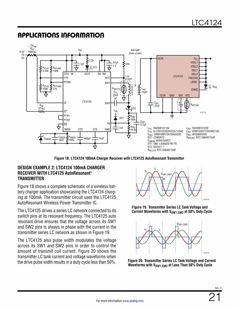
DESIGN EXAMPLE 2: LTC4124 100mA CHARGER RECEIVER WITH LTC4125 AutoResonant® TRANSMITTER
Figure 18 shows a complete schematic of a wireless bat-tery charger application showcasing the LTC4124 charg-ing at 100mA. The transmitter circuit uses the LTC4125 AutoResonant Wireless Power Transmitter IC.
The LTC4125 drives a series LC network connected to its switch pins at its resonant frequency. The LTC4125 auto resonant drive ensures that the voltage across its SW1 and SW2 pins is always in phase with the current in the transmitter series LC network as shown in Figure 19.
The LTC4125 also pulse width modulates the voltage across its SW1 and SW2 pins in order to control the amount of transmit coil current. Figure 20 shows the transmitter LC tank current and voltage waveforms when the drive pulse width results in a duty cycle less than 50%.
Figure 18.
CTX33nFx2
RNTCRX
FTH
PTHM
IS–
IS+
PTH1
PTH2
EN
NTC
SW1
SW2
FB
LTC4124
4124 F18
RPTHM221k
RFTH2100k
RFTH13.24k
2.2k
680pFDIMONCIMON10nF
1µF 47µFx 2
RIN374Ω
RIS180mΩ
IIN
15nF
1nF
CFB10.1µF
DC1
DT2
DT1
RFB1100k
RIMON100k
RFB216.5k
LTX6.5µH
VIN
VIN
RPTHM1100k
4.5VTO5V
100k
RNTCTX
VCCVSEL1VSEL2ISEL1ISEL2
PRECHGLBSEL
CHRG
ACIN
DCIN GND BAT NTC
DRX
CRX33nF
LRX13µH
+
AIR GAP3mm ±1mm
LTC4125
IMON CTD CTS GND
STATINDTH IN1 IN2
LTX: 760308101104 CTX: 2x C2012C0G2A333J125AC CFB1: GRM188R72A104KA35D DC1: CDBQR70DIMON: ADR510ARTZDT1: SML-LX0603S1W-TRDT2: BAS521-7RNTCTX: NTC G064EF104F
LRX: 760308101220CRX: GRM155R71H333KE14DDRX: APG0603VGCRNTCRX: NTC G064EF104F
LTC4124 100mA Charger Receiver with LTC4125 AutoResonant Transmitter
Figure 19.
4124 F19
VLIL
VSW1,SW2
Transmitter Series LC Tank Voltage and Current Waveforms with VSW1,SW2 at 50% Duty Cycle
Figure 20.
4124 F20
VL IL
VSW1,SW2
Transmitter Series LC Tank Voltage and Current Waveforms with VSW1,SW2 at Less Than 50% Duty Cycle
LTC4124
22Rev. A
For more information www.analog.com
APPLICATIONS INFORMATIONThe LTC4125 also features the ability to sense the load at the receiver which allows it to go to a low power operating state in the absence of a receiver. Furthermore, it has a for-eign object detection feature which prevents inadvertent wireless transmission of power to a conductive foreign object. Refer to the LTC4125 data sheet for more details on the LTC4125 operation and applications.
The steps needed to determine each of the component val-ues for the circuit shown in Figure 18 are reviewed here:
1. Determine the receiver resonant frequency and set component values for the receiver LC tank:
Similar to the first design example, the resonant fre-quency should be selected such that it is at least a factor of 5 below the self-resonant frequency of the coils and within the capability of the transmitter driver circuit. In this example, the self-resonant frequency of the RX coil is 19MHz and of the TX coil is 20MHz. So a factor 5 below 19MHz is 3.8MHz.
The LTC4125 transmitter IC has a maximum switch-ing frequency of 320kHz. It is best practice to select a resonant frequency that yields a low component count on the receiver to ensure the smallest footprint.
In this example, 240kHz is selected as the receiver resonant frequency. At 240kHz, the tank capacitance (CRX) required with the selected receive coil (13μH) is 33nF.
Following the guidance on selecting the resonant capacitor, in this particular example a 33nF capacitor with a 50V voltage rating and a small 0402 footprint is chosen.
2. Set the transmitter LC tank component values to match the receiver resonant frequency.
The transmit LC tank frequency (fTX-TANK) is also set at 240kHz. The transmit coil (LTX) used in the example is 6.5μH. The value of transmit tank capacitance (CTX) can be calculated:
CTX =
1
4 • π2 • f 2TX−TANK • LTX
= 66nF
The recommended rating for CTX capacitors in this particular example is 100V with 5% (or better) tolerance.
3. Determine the minimum pulse width of the transmit-ter driver required to deliver the required power at the receiver under the worst-case coupling conditions with maximum load.
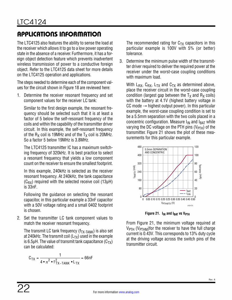
With LRX, CRX, LTX and CTX as determined above, place the receiver circuit in the worst-case coupling condition (largest gap between the TX and RX coils) with the battery at 4.1V (highest battery voltage in CC mode → highest output power). In this particular example, the worst-case coupling condition is set to be a 5.5mm separation with the two coils placed in a concentric configuration. Measure IIN and IBAT while varying the DC voltage on the PTH pins (VPTH) of the transmitter. Figure 21 shows the plot of these mea-surements for this particular example.
Figure 21.
VPTH@TX (V)0
I IN@
TX (m
A)
IBAT@RX (m
A)
480
320
400
160
240
80
0
120
80
100
40
60
20
00.15 0.450.05 0.25
4124 F21
0.500.35 0.400.10 0.300.20
5.5mm SEPARATIONAND CONCENTRIC
IBATIVIN
IIN and IBAT vs VPTH
From Figure 21, the minimum voltage required at VPTH (VPTHM)for the receiver to have the full charge current is 0.43V. This corresponds to 13% duty cycle at the driving voltage across the switch pins of the transmitter circuit.
LTC4124
23Rev. A
For more information www.analog.com
APPLICATIONS INFORMATION4. Verify that at the minimum pulse width selected in
Step 3, the AC current through the transmit coil is well within its rating and that there is no excessive heating on the LTC4124 nor excessive negative voltage on the ACIN pin of the LTC4124.
With the minimum pulse width determined in the pre-vious step, place the receiver circuit at the best-case coupling condition (In this particular example, the best coupling condition is set to be 1.5mm separation with the TX and RX coils placed in a concentric config-uration.) with the battery pin set at 4.3V (zero charge current→ lowest output power). Measure IL-TX(RMS), ΔTLTC4124 and VACIN-MIN. With VPTH = 0.43V (from the previous step) and VBAT = 4.3V, at the best-case coupling condition and steady state, the measured parameters are as follows:
IL-TX(RMS) = 1.0A, ΔTLTC4124 = 32°C and VACIN-MIN = –8.5V. The IL-TX(RMS) is well below the 2.5A max rated current for the transmit coil (see the Wurth Elektonik 760308101104 data sheet for more information). The temperature rise of 32°C and the minimum negative voltage on the ACIN pin are well within the rated operating condition for the LTC4124.
This result is verified using the alternative formula provided in the Choosing Transmit Power Level section. Using the suggested method, the coupling value at the best coupling condition is 0.5. Using this coupling value, the predicted value of the minimum negative voltage developed on the ACIN is –8.5V. Therefore, the predicted maximum VVCC – VACIN is 14V as verified empirically.
5. Determine the values of RPTHM1 and RPTHM2 based on the minimum pulse width of the transmitter driver obtained in Step 3.
Set RPTHM1 = 100kΩ. RPTHM2 can be obtained using the following formula:
RPTHM2 =
32 • VPTHM2.4
⎢⎣⎢
⎥⎦⎥+ 0.5
32 –32 • VPTHM
2.4⎢⎣⎢
⎥⎦⎥+ 0.5⎛
⎝⎜⎞⎠⎟
•RPTHM1
= 20.8kΩ≈ 21kΩ (standard 1% resistor value)
Note the quantity in the floor function brackets should be rounded down to the nearest integer.
6. Determine the values of RIS, RIN, RIMON and CIMON for load detection at best coupling with minimum load.
With the same setup used in Step 4 and VBAT = 4.3V, the input current to the transmit board is measured as IIN = 240mA (ITH). With the voltage drop across the sense resistor RIS set to about 40mV, calculate RIS according to the following formula:
RIS =40mV
IIN=
40mV240mA
= 167mΩ
≈ 180mΩ (standard 1% sense resistor value)
RIN is set to be 374Ω such that with 40mV across RIS, the IMON pin will source 107µA. This source current biases DIMON to generate 1V at the IMON pin for load detection. CIMON is set to be 10nF to provide some filtering on the IMON pin voltage, and RIMON is set to 100kΩ to discharge CIMON when the source current on the IMON pin is not present.
LTC4124
24Rev. A
For more information www.analog.com
APPLICATIONS INFORMATION7. Determine the value of CTS for step duration during
the LTC4125 load detection.
Set the step duration to 50ms, approximately about 5 times the observed VIMON settling time.
CTS = 5 •10µA • TS32 • 1.2V
= 1.3 × 10⁻⁶ • TS s( )
≈ 15nF (standard capacitor value)
8. Determine the value of RFB1 and RFB2 for no receiver detection.
With the minimum pulse width as determined in Step 3 and no receiver, measure IIN and VLC-TX ampli-tude. In this particular example, with no RX present, at VPTH = 0.43V: IIN = 580mA and |VLC-TX| = 40V.
The same measurement is done with a receiver at the worst coupling condition (largest gap between the TX and RX coils) with the battery pin set at 4.3V (zero charge current → lowest output power). In this particular example, using setup 4 at VPTH = 0.43V, IIN = 450mA and |VLC-TX| = 25V .
At the VPTH determined in step 3, the voltage at the transmitter resonant tank with no receiver is 40V (VLC-TX-MAX), and with a receiver at minimum load, it is 25V (VLC-TX-MIN). Using the formula provided in the LTC4125 data sheet, RFB1 and RFB2 can be calculated as follows:
VLC−TX−MIN – VDVIN
– 1<RFB1RFB2
<VLC−TX−MAX – VD
VIN– 1t
25V – 1V5V
– 1<RFB1RFB2
<40V – 1V
5V– 1
3.8 <RFB1RFB2
< 6.8
Therefore, set the ratio to be 6. Since the recom-mended total RFB1 + RFB2 resistance is about 100kΩ, set RFB1 = 100kΩ and RFB2 = 16.5kΩ.
9. Determine the value of RFTH1 and RFTH2 for foreign object detection.
As outlined in steps 1 and 2, the resonant frequency selected is 240kHz. However, the operating frequency of the two coupled resonant LC at the TX and RX under heavy load at the best coupling condition is as high as 300kHz. Therefore, set the foreign object detection frequency threshold at 310kHz, about 3% above the highest operating frequency. Set RFTH2 = 100kΩ and RFTH1 according to the following formula:
RFTH1 =320kHz
fLIM– 1
⎛⎝⎜
⎞⎠⎟
•R FTH2
= 320kHz310kHz
– 1⎛⎝⎜
⎞⎠⎟ • 100kΩ = 3.23kΩ
≈ 3.24kΩ (standard 1% resistor value)
10. Determine the value of CTD for the delay between each load detection attempt.
Set the wait time to 5 seconds. Then, the CTD value is calculated using the following formula:
CTD =
10µA • TD
65 × 103 • 1.2V= 1.3 × 10⁻¹⁰ • 5 ≈ 680pF
LTC4124
25Rev. A
For more information www.analog.com
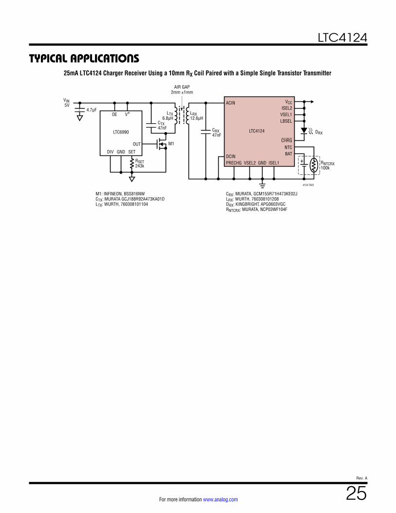
TYPICAL APPLICATIONS25mA LTC4124 Charger Receiver Using a 10mm RX Coil Paired with a Simple Single Transistor Transmitter
RNTCRX100k
RSET243k
LTC4124
4124 TA02
VCCISEL2
VSEL1LBSEL
CHRG
ACIN
NTCBATDCIN
PRECHG +VSEL2 GND ISEL1
DIV GND SET
OUT
LRX12.6µH
DRXLTC6990
M1: INFINEON, BSS816NWCTX: MURATA GCJ188R92A473KA01D LTX: WURTH, 760308101104
CRX: MURATA, GCM155R71H473KE02J LRX: WURTH, 760308101208 DRX: KINGBRIGHT, APG0603VGCRNTCRX: MURATA, NCP03WF104F
M1
VIN5V
LTX6.8µH
CTX47nF CRX
47nF
4.7µFV+OE
AIR GAP2mm ±1mm
LTC4124
26Rev. A
For more information www.analog.com
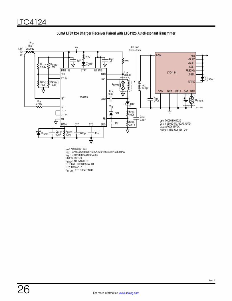
50mA LTC4124 Charger Receiver Paired with LTC4125 AutoResonant Transmitter
CTX90nF
RNTCRX
FTH
PTHM
IS–
IS+
PTH1
PTH2
EN
NTC
SW1
SW2
FB
LTC4124
4124 TA03
RPTHM216.5k
RFTH2100k
RFTH13.24k
2.2k
680pFDIMONCIMON10nF
1µF 47µFx 2
RIN374Ω
RIS250mΩ
IIN
15nF
1nF
CFB10.1µF
DC1
DT2
DT1
RFB1100k
RIMON100k
RFB222.1k
LTX6.8µH
VIN
VIN
RPTHM1100k
4.5VTO5V
100k
RNTCTX
VCCVSEL2VSEL1ISEL1
PRECHGLBSEL
CHRG
ACIN
DCIN ISEL2GND BAT NTC
DRX
CRX47nF
LRX12.6µH
+
AIR GAP3mm ±1mm
LTC4125
IMON CTD CTS GND
STATINDTH IN1 IN2
LTX: 760308101104 CTX: C3216C0G1H683J160AA, C3216C0G1H223J060AA CFB1: GRM188R72A104KA35D DC1: CDBQR70DIMON: ADR510ARTZDT1: SML-LX0603S1W-TRDT2: BAS521-7RNTCTX: NTC G064EF104F
LRX: 760308101220CRX: C0805C473J3GACAUTODRX: APG0603VGCRNTCRX: NTC G064EF104F
LTC4124
27Rev. A
For more information www.analog.com
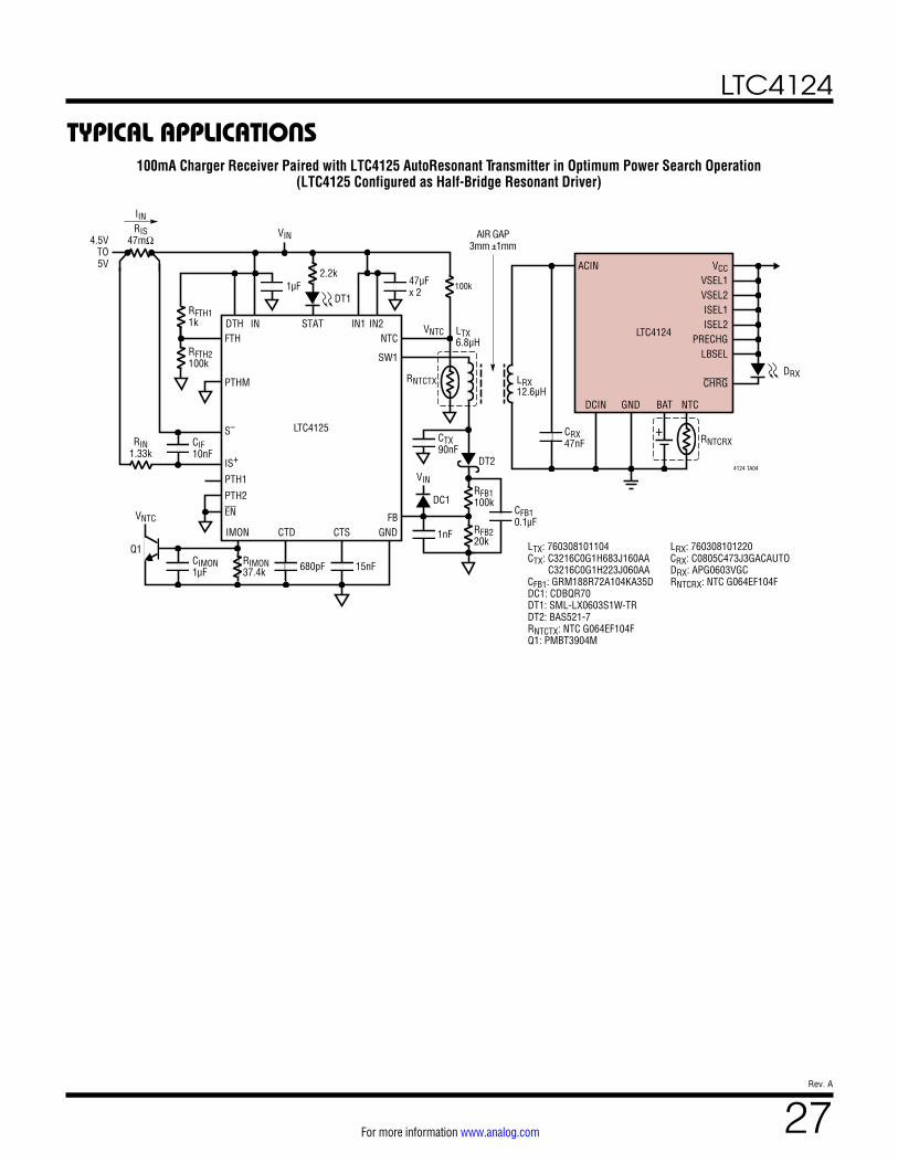
TYPICAL APPLICATIONS100mA Charger Receiver Paired with LTC4125 AutoResonant Transmitter in Optimum Power Search Operation
(LTC4125 Configured as Half-Bridge Resonant Driver)
CTX90nF
RNTCRX
FTH
PTHM
NTC
SW1
LTC4124
FB
4124 TA04
RFTH11k
RFTH2100k
2.2k
680pFCIMON1µF
1µF
CIF10nF
47µFx 2
RIN1.33k
RIS47mΩ
IIN
15nF
1nF
CFB10.1µF
DC1
DT2
DT1
RFB1100k
RIMON37.4k
RFB220k
LTX6.8µH
VIN
VIN
VNTC
VNTC
4.5VTO5V
100k
RNTCTX
VCCVSEL1VSEL2ISEL1ISEL2
PRECHGLBSEL
CHRG
ACIN
DCIN GND BAT NTC
DRX
CRX47nF
LRX12.6µH
+
AIR GAP3mm ±1mm
Q1
LTC4125
IMON CTD CTS GND
STATINDTH IN1 IN2
LTX: 760308101104 CTX: C3216C0G1H683J160AA C3216C0G1H223J060AACFB1: GRM188R72A104KA35D DC1: CDBQR70DT1: SML-LX0603S1W-TRDT2: BAS521-7RNTCTX: NTC G064EF104FQ1: PMBT3904M
LRX: 760308101220CRX: C0805C473J3GACAUTODRX: APG0603VGCRNTCRX: NTC G064EF104F
S–
IS+
PTH1
PTH2
EN
LTC4124
28Rev. A
For more information www.analog.com
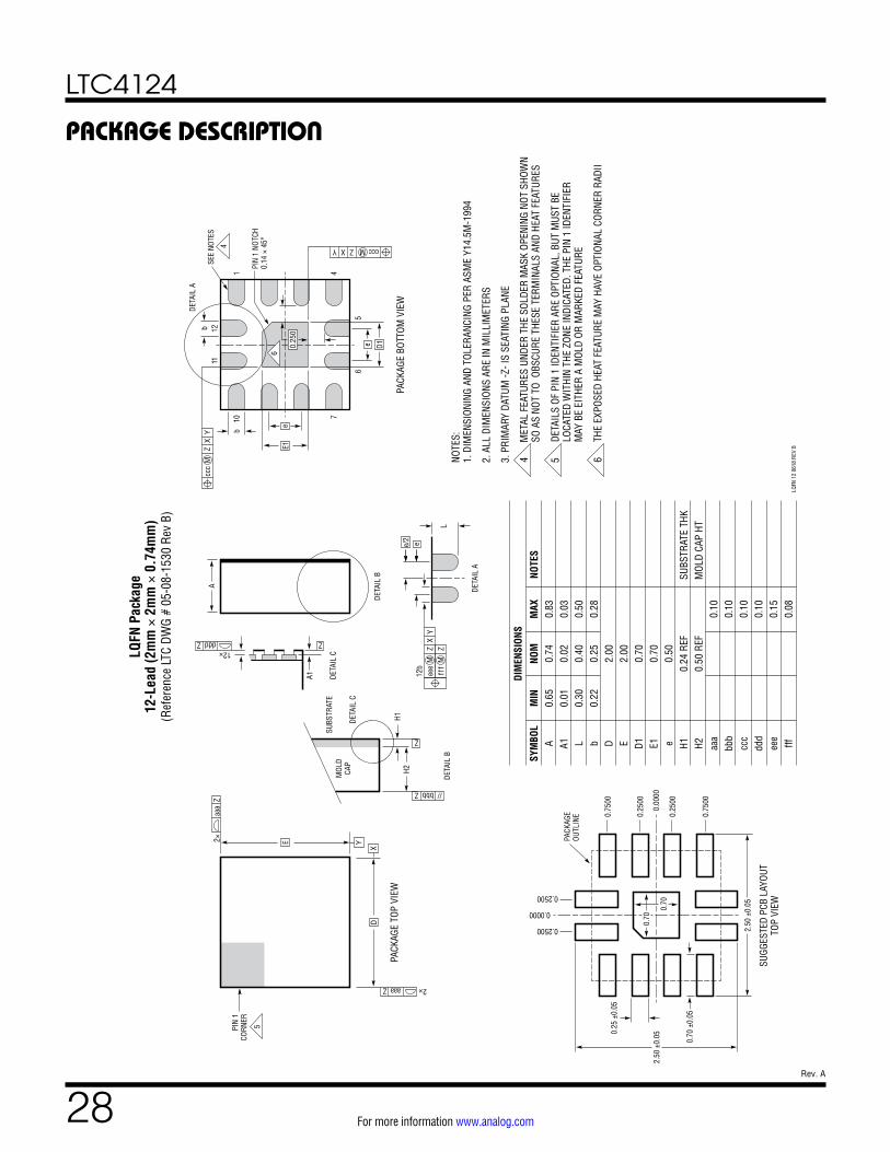
PACKAGE DESCRIPTIONLQ
FN P
acka
ge12
-Lea
d (2
mm
× 2
mm
× 0
.74m
m)
(Ref
eren
ce L
TC D
WG
# 05
-08-
1530
Rev
B)
DETA
IL B
A
PACK
AGE
TOP
VIEW
5PIN
1CO
RNER
Y
X
aaa
Z2×
12b
PACK
AGE
BOTT
OM V
IEW
4
6
SEE
NOTE
S
E
D
b
e
e
b
E1
D1
DETA
IL B
SUBS
TRAT
EM
OLD
CAP
// bbb Z
ZH2
H1
L
DETA
IL A
DETA
IL C
SUGG
ESTE
D PC
B LA
YOUT
TOP
VIEW0.0000
0.00
00
0.75
00
0.25
00
0.25
00
0.75
00
0.2500
0.2500
DETA
IL A
PIN
1 NO
TCH
0.14
× 4
5°
1112
65
1 4
10 7
aaa Z 2×
MX
YZ
ccc
MXY Z ccc
MX
YZ
eee
MZ
fff
PACK
AGE
OUTL
INE
0.25
±0.
05
0.70
±0.
05
2.50
±0.
05
2.50
±0.
05
LQFN
12
0618
REV
B
0.25
0
0.70
0.70
ddd Z12×
Z
A1 DETA
IL C
SYM
BOL
A A1 L b D E D1 E1 e H1 H2 aaa
bbb
ccc
ddd
eee
fff
MIN
0.65
0.01
0.30
0.22
NOM
0.74
0.02
0.40
0.25
2.00
2.00
0.70
0.70
0.50
0.24
REF
0.50
REF
MAX
0.83
0.03
0.50
0.28
0.10
0.10
0.10
0.10
0.15
0.08
NOTE
S
DIM
ENSI
ONS
NOTE
S:1.
DIM
ENSI
ONIN
G AN
D TO
LERA
NCIN
G PE
R AS
ME
Y14.
5M-1
994
2. A
LL D
IMEN
SION
S AR
E IN
MIL
LIM
ETER
S
3. P
RIM
ARY
DATU
M -Z
- IS
SEAT
ING
PLAN
E
MET
AL F
EATU
RES
UNDE
R TH
E SO
LDER
MAS
K OP
ENIN
G NO
T SH
OWN
SO
AS
NOT
TO O
BSCU
RE T
HESE
TER
MIN
ALS
AND
HEAT
FEA
TURE
S
54
DETA
ILS
OF P
IN 1
IDEN
TIFI
ER A
RE O
PTIO
NAL,
BUT
MUS
T BE
LO
CATE
D W
ITHI
N TH
E ZO
NE IN
DICA
TED.
THE
PIN
1 ID
ENTI
FIER
M
AY B
E EI
THER
A M
OLD
OR M
ARKE
D FE
ATUR
E
6TH
E EX
POSE
D HE
AT F
EATU
RE M
AY H
AVE
OPTI
ONAL
COR
NER
RADI
I
ee/2
SUBS
TRAT
E TH
KM
OLD
CAP
HT
LTC4124
29Rev. A
For more information www.analog.com
Information furnished by Analog Devices is believed to be accurate and reliable. However, no responsibility is assumed by Analog Devices for its use, nor for any infringements of patents or other rights of third parties that may result from its use. Specifications subject to change without notice. No license is granted by implication or otherwise under any patent or patent rights of Analog Devices.
REV DATE DESCRIPTION PAGE NUMBER
A 11/19 Changed Battery Charging VUVCL Condition Changed Battery Discharge PowerPath Forward Regulation Voltage Condition Changed Disconnect Battery Leakage Curve Conditions Changed Application Circuits Cap Values
3 4 5
26, 27
REVISION HISTORY
LTC4124
30Rev. A
For more information www.analog.com ANALOG DEVICES, INC. 2019
11/19www.analog.com
RELATED PARTS
TYPICAL APPLICATION
PART NUMBER DESCRIPTION COMMENTS
LTC4123 Low Power Wireless Charger for Hearing Aids Wireless NiMH Charger, Temperature Compensated Charge Voltage, 1.5V at 25°C, 25mA Charge Current, 2mm × 2mm DFN-6 Package.
LTC4126 Low Power Li-Ion Wireless Charger with Step Down Regulator for Hearing Aids
Wireless Single Cell Li-Ion Charger, Internal Temperature Qualified Charging, 4.2V at 25°C, 7.5mA Charge Current, Integrated High Efficiency 1.2V Regulator, 2mm × 2mm LQFN Package.
LTC4070 Li-Ion/Polymer Shunt Battery Charger System Low Operating Current (450nA), 1% Float Voltage Accuracy Over Full Temperature and Shunt Current Range, 50mA Maximum Internal Shunt Current (500mA with External PFET), Pin-Selectable Float Voltages: 4.0V, 4.1V, 4.2V. Ultralow Power Pulsed NTC Float Conditioning for Li-Ion/Polymer Protection, 8-Lead 2mm × 3mm DFN and MSOP.
LTC4071 Li-Ion/Polymer Shunt Battery Charger System with Low Battery Disconnect
Integrated Pack Protection, <10nA Low Battery Disconnect Protects Battery from Over-Discharge. Low Operating Current (550nA), 1% Float Voltage Accuracy Over Full Temperature and Shunt Current Range, 50mA Maximum Internal Shunt Current, Pin-Selectable Float Voltages: 4.0V, 4.1V, 4.2V. Ultralow Power Pulsed NTC Float Conditioning for Li-Ion/Polymer Protection, 8-Lead 2mm × 3mm DFN and MSOP.
LTC6990 TimerBlox: Voltage-Controlled Silicon Oscillator Fixed-Frequency or Voltage-Controlled Operation.
LTC4125 5W AutoResonant Wireless Power Transmitter Monolithic AutoResonant™ Full Bridge Driver. Transmit Power Automatically Adjusts to Receiver Load, Foreign Object Detection, Wide Operating Switching Frequency Range: 50kHz-250kHz, Input Voltage Range 3V to 5.5V, 20-Lead 4mm × 5mm QFN Package.
LTC4120 Wireless Power Receiver and 400mA Buck Battery Charger
Wireless 1 to 2 Cell Li-Ion Charger, 400mA Charge Current, Dynamic Harmonization Control, Wide Input Range: 12.5V – 40V, 3mm × 3mm QFN-16 Package.
Up to Four LTC4124, 10mA Minimum Size Charger Receivers with a Single LTC4125 AutoResonant Transmitter
CTX40.8nF RNTCRX
100k
FTH
PTHM
IS–
IS+
PTH1
PTH2
EN
NTC
SW1
SW2
FB
LTC4124
UP TO 4x
4124 TA04
RPTHM225.5k
RFTH2100k
RFTH137.4k
2.2k
680pFDT3 CIMON10nF
1µF 47µFx 2
RIN332Ω
RIS120mΩ
IIN
15nF
0.1µF
AIR GAP8mm ±1mm
CFB10.1µF
DC1
DT2
DT1
RFB110k
RIMON54.9k
RFB21.87k
LTX12µH
VIN
VIN
RPTHM1100k
4.5VTO5V
100k
RNTCTX
VCCVSEL1LBSEL
CHRG
ACIN
NTCBAT
DCINPRECHG
+VSEL2 GND ISEL1 ISEL2
DRXCRX68nF
LRX7.2µH
LTC4125
IMON CTD CTS GND
STATINDTH IN1 IN2
LTX: 760308104113 CTX: GA0603Y393KXBAP31G GRM155R72A182KA01DCFB1: GRM188R72A104KA35DDC1: CDBQR70DT1: SML-LX0603S1W-TRDT2: BAS521-7DT3: ADR510ARTZRNTCTX: NTCG064EF104F
LRX: 760308101216 CRX: GRM155R71H683KE14JDRX: APG0603VGCRNTCRX: NTCG064EF104F