ltc6804-1/ltc6804-2 – multicell battery monitors€¦ · measurement error (mv) 1.5 25 680412...
TRANSCRIPT
LTC6804-1/LTC6804-2
1680412fc
For more information www.linear.com/LTC6804-1
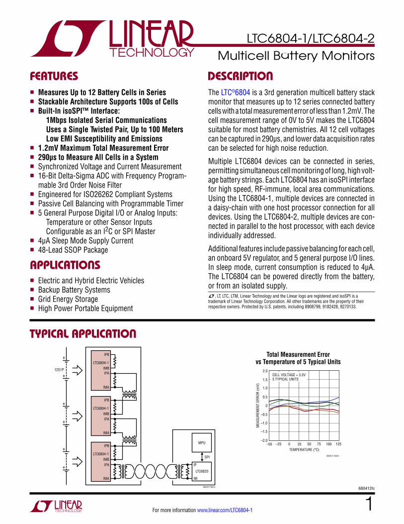
Typical applicaTion
FeaTures DescripTion
Multicell Battery Monitors
The LTC®6804 is a 3rd generation multicell battery stack monitor that measures up to 12 series connected battery cells with a total measurement error of less than 1.2mV. The cell measurement range of 0V to 5V makes the LTC6804 suitable for most battery chemistries. All 12 cell voltages can be captured in 290µs, and lower data acquisition rates can be selected for high noise reduction.
Multiple LTC6804 devices can be connected in series, permitting simultaneous cell monitoring of long, high volt-age battery strings. Each LTC6804 has an isoSPI interface for high speed, RF-immune, local area communications. Using the LTC6804-1, multiple devices are connected in a daisy-chain with one host processor connection for all devices. Using the LTC6804-2, multiple devices are con-nected in parallel to the host processor, with each device individually addressed.
Additional features include passive balancing for each cell, an onboard 5V regulator, and 5 general purpose I/O lines. In sleep mode, current consumption is reduced to 4µA. The LTC6804 can be powered directly from the battery, or from an isolated supply.L, LT, LTC, LTM, Linear Technology and the Linear logo are registered and isoSPI is a trademark of Linear Technology Corporation. All other trademarks are the property of their respective owners. Protected by U.S. patents, including 8908799, 9182428, 9270133.
Total Measurement Error vs Temperature of 5 Typical Units
applicaTions
n Measures Up to 12 Battery Cells in Series n Stackable Architecture Supports 100s of Cells n Built-In isoSPI™ Interface:
1Mbps Isolated Serial Communications Uses a Single Twisted Pair, Up to 100 Meters Low EMI Susceptibility and Emissions
n 1.2mV Maximum Total Measurement Error n 290µs to Measure All Cells in a System n Synchronized Voltage and Current Measurement n 16-Bit Delta-Sigma ADC with Frequency Program-
mable 3rd Order Noise Filter n Engineered for ISO26262 Compliant Systems n Passive Cell Balancing with Programmable Timer n 5 General Purpose Digital I/O or Analog Inputs:
Temperature or other Sensor Inputs Configurable as an I2C or SPI Master
n 4μA Sleep Mode Supply Current n 48-Lead SSOP Package
n Electric and Hybrid Electric Vehicles n Backup Battery Systems n Grid Energy Storage n High Power Portable Equipment
LTC6820
LTC6804-1
MPU
IP
••
••
• • • •
SPI
IM
IPA
IMA
680412 TA01a
IPB
IMB
LTC6804-1
IMA
IPA
ILP
IPB
IMB
LTC6804-1
IMA
IPB
IMBIPA
12S1P
+
+
+
+
+
+
TEMPERATURE (°C)–50
MEA
SURE
MEN
T ER
ROR
(mV)
1.5
25
680412 TA01b
0
–1.0
–25 0 50
–1.5
–2.0
2.0
1.0
0.5
–0.5
75 100 125
CELL VOLTAGE = 3.3V5 TYPICAL UNITS
LTC6804-1/LTC6804-2
2680412fc
For more information www.linear.com/LTC6804-1
Table oF conTenTsFeatures ..................................................... 1Applications ................................................ 1Typical Application ........................................ 1Description.................................................. 1Absolute Maximum Ratings .............................. 3Pin Configuration .......................................... 3Order Information .......................................... 4Electrical Characteristics ................................. 4Pin Functions .............................................. 17Block Diagram ............................................. 18Operation................................................... 20
State Diagram .........................................................20LTC6804 Core State Descriptions ...........................20isoSPI State Descriptions ....................................... 21Power Consumption ............................................... 21ADC Operation ........................................................ 21Data Acquisition System Diagnostics .....................26Watchdog and Software Discharge Timer ..............30I2C/SPI Master on LTC6804 Using GPIOS .............. 31Serial Interface Overview ........................................354-Wire Serial Peripheral Interface (SPI) Physical Layer ........................................................362-Wire Isolated Interface (isoSPI) Physical Layer ...36
Data Link Layer .......................................................44Network Layer ........................................................44Programming Examples .........................................54Simple Linear Regulator .........................................58Improved Regulator Power Efficiency .....................58Fully Isolated Power ................................................59Reading External Temperature Probes ....................59Expanding the Number of Auxiliary Measurements ........................................................60Internal Protection Features ....................................60Filtering of Cell and GPIO Inputs .............................60Cell Balancing with Internal Mosfets .......................62Cell Balancing with External MOSFETS...................62Discharge Control During Cell Measurements ........62Power Dissipation and Thermal Shutdown .............63Method to Verify Balancing Circuitry ......................63Current Measurement with a Hall Effect Sensor .....66Current Measurement with a Shunt Resistor ..........66Using the LTC6804 with Less Than 12 Cells ...........67
Package Description ..................................... 76Revision History .......................................... 77Typical Application ....................................... 78Related Parts .............................................. 78
LTC6804-1/LTC6804-2
3680412fc
For more information www.linear.com/LTC6804-1
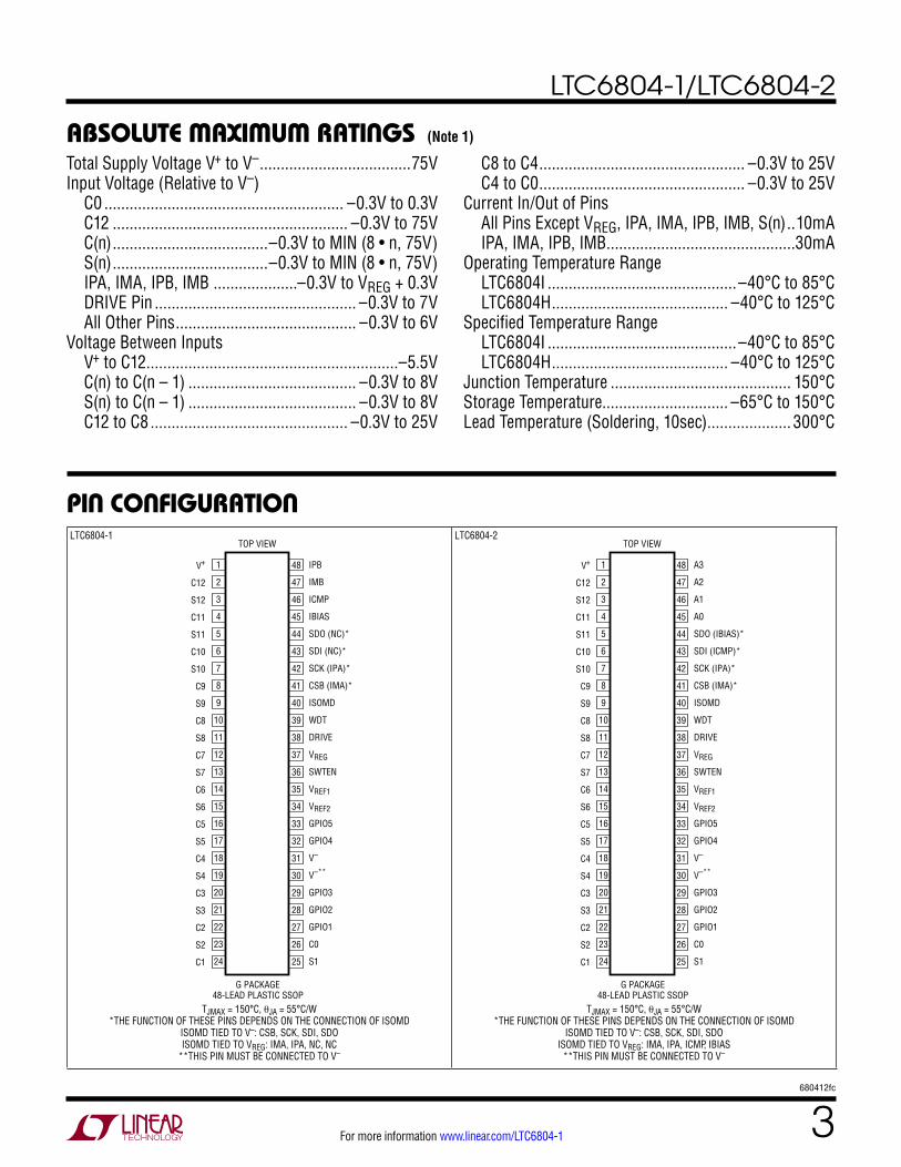
absoluTe MaxiMuM raTingsTotal Supply Voltage V+ to V– ....................................75VInput Voltage (Relative to V–)
C0 ......................................................... –0.3V to 0.3V C12 ........................................................ –0.3V to 75V C(n) .....................................–0.3V to MIN (8 • n, 75V) S(n) .....................................–0.3V to MIN (8 • n, 75V) IPA, IMA, IPB, IMB ....................–0.3V to VREG + 0.3V
DRIVE Pin ................................................ –0.3V to 7V All Other Pins ........................................... –0.3V to 6V
Voltage Between Inputs V+ to C12 ............................................................–5.5V
C(n) to C(n – 1) ........................................ –0.3V to 8V S(n) to C(n – 1) ........................................ –0.3V to 8V C12 to C8 ............................................... –0.3V to 25V
(Note 1)
pin conFiguraTion
C8 to C4 ................................................. –0.3V to 25V C4 to C0 ................................................. –0.3V to 25V
Current In/Out of Pins All Pins Except VREG, IPA, IMA, IPB, IMB, S(n) ..10mA IPA, IMA, IPB, IMB .............................................30mA
Operating Temperature Range LTC6804I .............................................–40°C to 85°C LTC6804H .......................................... –40°C to 125°C
Specified Temperature Range LTC6804I .............................................–40°C to 85°C LTC6804H .......................................... –40°C to 125°C
Junction Temperature ........................................... 150°CStorage Temperature.............................. –65°C to 150°CLead Temperature (Soldering, 10sec).................... 300°C
LTC6804-1 LTC6804-2
1
2
3
4
5
6
7
8
9
10
11
12
13
14
15
16
17
18
19
20
21
22
23
24
TOP VIEW
G PACKAGE48-LEAD PLASTIC SSOP
48
47
46
45
44
43
42
41
40
39
38
37
36
35
34
33
32
31
30
29
28
27
26
25
V+
C12
S12
C11
S11
C10
S10
C9
S9
C8
S8
C7
S7
C6
S6
C5
S5
C4
S4
C3
S3
C2
S2
C1
IPB
IMB
ICMP
IBIAS
SDO (NC)*
SDI (NC)*
SCK (IPA)*
CSB (IMA)*
ISOMD
WDT
DRIVE
VREG
SWTEN
VREF1
VREF2
GPIO5
GPIO4
V–
V–**
GPIO3
GPIO2
GPIO1
C0
S1
TJMAX = 150°C, θJA = 55°C/W
*THE FUNCTION OF THESE PINS DEPENDS ON THE CONNECTION OF ISOMD ISOMD TIED TO V–: CSB, SCK, SDI, SDO ISOMD TIED TO VREG: IMA, IPA, NC, NC
**THIS PIN MUST BE CONNECTED TO V–
1
2
3
4
5
6
7
8
9
10
11
12
13
14
15
16
17
18
19
20
21
22
23
24
TOP VIEW
G PACKAGE48-LEAD PLASTIC SSOP
48
47
46
45
44
43
42
41
40
39
38
37
36
35
34
33
32
31
30
29
28
27
26
25
V+
C12
S12
C11
S11
C10
S10
C9
S9
C8
S8
C7
S7
C6
S6
C5
S5
C4
S4
C3
S3
C2
S2
C1
A3
A2
A1
A0
SDO (IBIAS)*
SDI (ICMP)*
SCK (IPA)*
CSB (IMA)*
ISOMD
WDT
DRIVE
VREG
SWTEN
VREF1
VREF2
GPIO5
GPIO4
V–
V–**
GPIO3
GPIO2
GPIO1
C0
S1
TJMAX = 150°C, θJA = 55°C/W
*THE FUNCTION OF THESE PINS DEPENDS ON THE CONNECTION OF ISOMD ISOMD TIED TO V–: CSB, SCK, SDI, SDO
ISOMD TIED TO VREG: IMA, IPA, ICMP, IBIAS **THIS PIN MUST BE CONNECTED TO V–
LTC6804-1/LTC6804-2
4680412fc
For more information www.linear.com/LTC6804-1
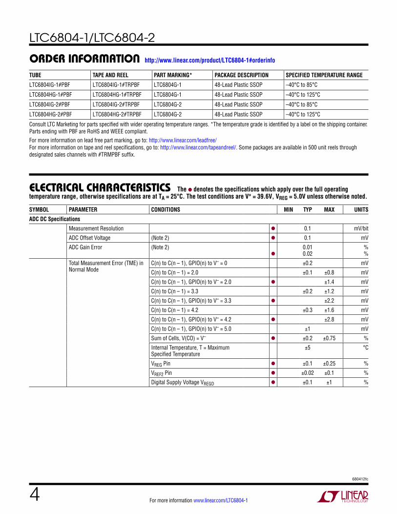
orDer inForMaTion
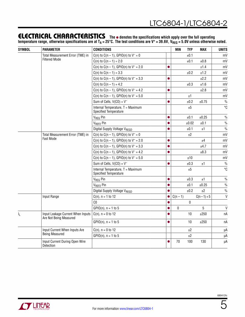
elecTrical characTerisTics
SYMBOL PARAMETER CONDITIONS MIN TYP MAX UNITS
ADC DC Specifications
Measurement Resolution l 0.1 mV/bit
ADC Offset Voltage (Note 2) l 0.1 mV
ADC Gain Error (Note 2)
l
0.01 0.02
% %
Total Measurement Error (TME) in Normal Mode
C(n) to C(n – 1), GPIO(n) to V– = 0 ±0.2 mV
C(n) to C(n – 1) = 2.0 ±0.1 ±0.8 mV
C(n) to C(n – 1), GPIO(n) to V– = 2.0 l ±1.4 mV
C(n) to C(n – 1) = 3.3 ±0.2 ±1.2 mV
C(n) to C(n – 1), GPIO(n) to V– = 3.3 l ±2.2 mV
C(n) to C(n – 1) = 4.2 ±0.3 ±1.6 mV
C(n) to C(n – 1), GPIO(n) to V– = 4.2 l ±2.8 mV
C(n) to C(n – 1), GPIO(n) to V– = 5.0 ±1 mV
Sum of Cells, V(CO) = V– l ±0.2 ±0.75 %
Internal Temperature, T = Maximum Specified Temperature
±5 °C
VREG Pin l ±0.1 ±0.25 %
VREF2 Pin l ±0.02 ±0.1 %
Digital Supply Voltage VREGD l ±0.1 ±1 %
The l denotes the specifications which apply over the full operating temperature range, otherwise specifications are at TA = 25°C. The test conditions are V+ = 39.6V, VREG = 5.0V unless otherwise noted.
TUBE TAPE AND REEL PART MARKING* PACKAGE DESCRIPTION SPECIFIED TEMPERATURE RANGE
LTC6804IG-1#PBF LTC6804IG-1#TRPBF LTC6804G-1 48-Lead Plastic SSOP –40°C to 85°C
LTC6804HG-1#PBF LTC6804HG-1#TRPBF LTC6804G-1 48-Lead Plastic SSOP –40°C to 125°C
LTC6804IG-2#PBF LTC6804IG-2#TRPBF LTC6804G-2 48-Lead Plastic SSOP –40°C to 85°C
LTC6804HG-2#PBF LTC6804HG-2#TRPBF LTC6804G-2 48-Lead Plastic SSOP –40°C to 125°C
Consult LTC Marketing for parts specified with wider operating temperature ranges. *The temperature grade is identified by a label on the shipping container. Parts ending with PBF are RoHS and WEEE compliant.For more information on lead free part marking, go to: http://www.linear.com/leadfree/ For more information on tape and reel specifications, go to: http://www.linear.com/tapeandreel/. Some packages are available in 500 unit reels through designated sales channels with #TRMPBF suffix.
http://www.linear.com/product/LTC6804-1#orderinfo
LTC6804-1/LTC6804-2
5680412fc
For more information www.linear.com/LTC6804-1
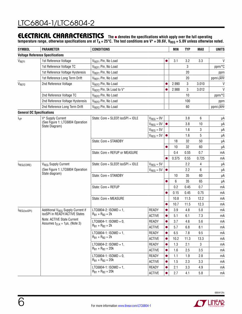
elecTrical characTerisTics
SYMBOL PARAMETER CONDITIONS MIN TYP MAX UNITS
Total Measurement Error (TME) in Filtered Mode
C(n) to C(n – 1), GPIO(n) to V– = 0 ±0.1 mV
C(n) to C(n – 1) = 2.0 ±0.1 ±0.8 mV
C(n) to C(n – 1), GPIO(n) to V– = 2.0 l ±1.4 mV
C(n) to C(n – 1) = 3.3 ±0.2 ±1.2 mV
C(n) to C(n – 1), GPIO(n) to V– = 3.3 l ±2.2 mV
C(n) to C(n – 1) = 4.2 ±0.3 ±1.6 mV
C(n) to C(n – 1), GPIO(n) to V– = 4.2 l ±2.8 mV
C(n) to C(n – 1), GPIO(n) to V– = 5.0 ±1 mV
Sum of Cells, V(CO) = V– l ±0.2 ±0.75 %
Internal Temperature, T = Maximum Specified Temperature
±5 °C
VREG Pin l ±0.1 ±0.25 %
VREF2 Pin l ±0.02 ±0.1 %
Digital Supply Voltage VREGD l ±0.1 ±1 %
Total Measurement Error (TME) in Fast Mode
C(n) to C(n – 1), GPIO(n) to V– = 0 ±2 mV
C(n) to C(n – 1), GPIO(n) to V– = 2.0 l ±4 mV
C(n) to C(n – 1), GPIO(n) to V– = 3.3 l ±4.7 mV
C(n) to C(n – 1), GPIO(n) to V– = 4.2 l ±8.3 mV
C(n) to C(n – 1), GPIO(n) to V– = 5.0 ±10 mV
Sum of Cells, V(CO) = V– l ±0.3 ±1 %
Internal Temperature, T = Maximum Specified Temperature
±5 °C
VREG Pin l ±0.3 ±1 %
VREF2 Pin l ±0.1 ±0.25 %
Digital Supply Voltage VREGD l ±0.2 ±2 %
Input Range C(n), n = 1 to 12 l C(n – 1) C(n – 1) + 5 V
C0 l 0
GPIO(n), n = 1 to 5 l 0 5 V
IL Input Leakage Current When Inputs Are Not Being Measured
C(n), n = 0 to 12 l 10 ±250 nA
GPIO(n), n = 1 to 5 l 10 ±250 nA
Input Current When Inputs Are Being Measured
C(n), n = 0 to 12 ±2 µA
GPIO(n), n = 1 to 5 ±2 µA
Input Current During Open Wire Detection
l 70 100 130 µA
The l denotes the specifications which apply over the full operating temperature range, otherwise specifications are at TA = 25°C. The test conditions are V+ = 39.6V, VREG = 5.0V unless otherwise noted.
LTC6804-1/LTC6804-2
6680412fc
For more information www.linear.com/LTC6804-1
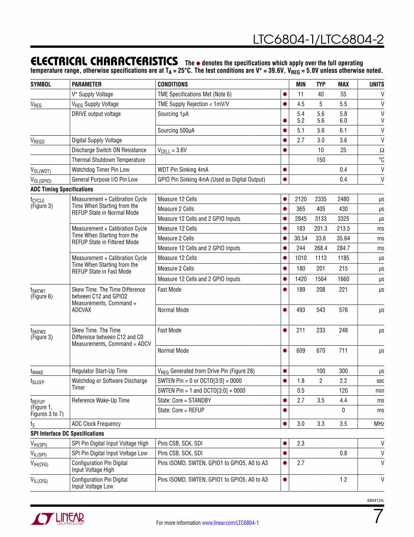
elecTrical characTerisTics
SYMBOL PARAMETER CONDITIONS MIN TYP MAX UNITS
Voltage Reference Specifications
VREF1 1st Reference Voltage VREF1 Pin, No Load l 3.1 3.2 3.3 V
1st Reference Voltage TC VREF1 Pin, No Load 3 ppm/°C
1st Reference Voltage Hysteresis VREF1 Pin, No Load 20 ppm
1st Reference Long Term Drift VREF1 Pin, No Load 20 ppm/√kHr
VREF2 2nd Reference Voltage VREF2 Pin, No Load l 2.990 3 3.010 V
VREF2 Pin, 5k Load to V– l 2.988 3 3.012 V
2nd Reference Voltage TC VREF2 Pin, No Load 10 ppm/°C
2nd Reference Voltage Hysteresis VREF2 Pin, No Load 100 ppm
2nd Reference Long Term Drift VREF2 Pin, No Load 60 ppm/√kHr
General DC Specifications
IVP V+ Supply Current (See Figure 1: LTC6804 Operation State Diagram)
State: Core = SLEEP, isoSPI = IDLE VREG = 0V 3.8 6 µA
VREG = 0V l 3.8 10 µA
VREG = 5V 1.6 3 µA
VREG = 5V l 1.6 5 µA
State: Core = STANDBY 18 32 50 µA
l 10 32 60 µA
State: Core = REFUP or MEASURE 0.4 0.55 0.7 mA
l 0.375 0.55 0.725 mA
IREG(CORE) VREG Supply Current(See Figure 1: LTC6804 Operation State diagram)
State: Core = SLEEP, isoSPI = IDLE VREG = 5V 2.2 4 µA
VREG = 5V l 2.2 6 µA
State: Core = STANDBY 10 35 60 µA
l 6 35 65 µA
State: Core = REFUP 0.2 0.45 0.7 mA
l 0.15 0.45 0.75 mA
State: Core = MEASURE 10.8 11.5 12.2 mA
l 10.7 11.5 12.3 mA
IREG(isoSPI) Additional VREG Supply Current if isoSPI in READY/ACTIVE StatesNote: ACTIVE State Current Assumes tCLK = 1µs, (Note 3)
LTC6804-2: ISOMD = 1, RB1 + RB2 = 2k
READY l 3.9 4.8 5.8 mA
ACTIVE l 5.1 6.1 7.3 mA
LTC6804-1: ISOMD = 0, RB1 + RB2 = 2k
READY l 3.7 4.6 5.6 mA
ACTIVE l 5.7 6.8 8.1 mA
LTC6804-1: ISOMD = 1, RB1 + RB2 = 2k
READY l 6.5 7.8 9.5 mA
ACTIVE l 10.2 11.3 13.3 mA
LTC6804-2: ISOMD = 1, RB1 + RB2 = 20k
READY l 1.3 2.1 3 mA
ACTIVE l 1.6 2.5 3.5 mA
LTC6804-1: ISOMD = 0, RB1 + RB2 = 20k
READY l 1.1 1.9 2.8 mA
ACTIVE l 1.5 2.3 3.3 mA
LTC6804-1: ISOMD = 1, RB1 + RB2 = 20k
READY l 2.1 3.3 4.9 mA
ACTIVE l 2.7 4.1 5.8 mA
The l denotes the specifications which apply over the full operating temperature range, otherwise specifications are at TA = 25°C. The test conditions are V+ = 39.6V, VREG = 5.0V unless otherwise noted.
LTC6804-1/LTC6804-2
7680412fc
For more information www.linear.com/LTC6804-1
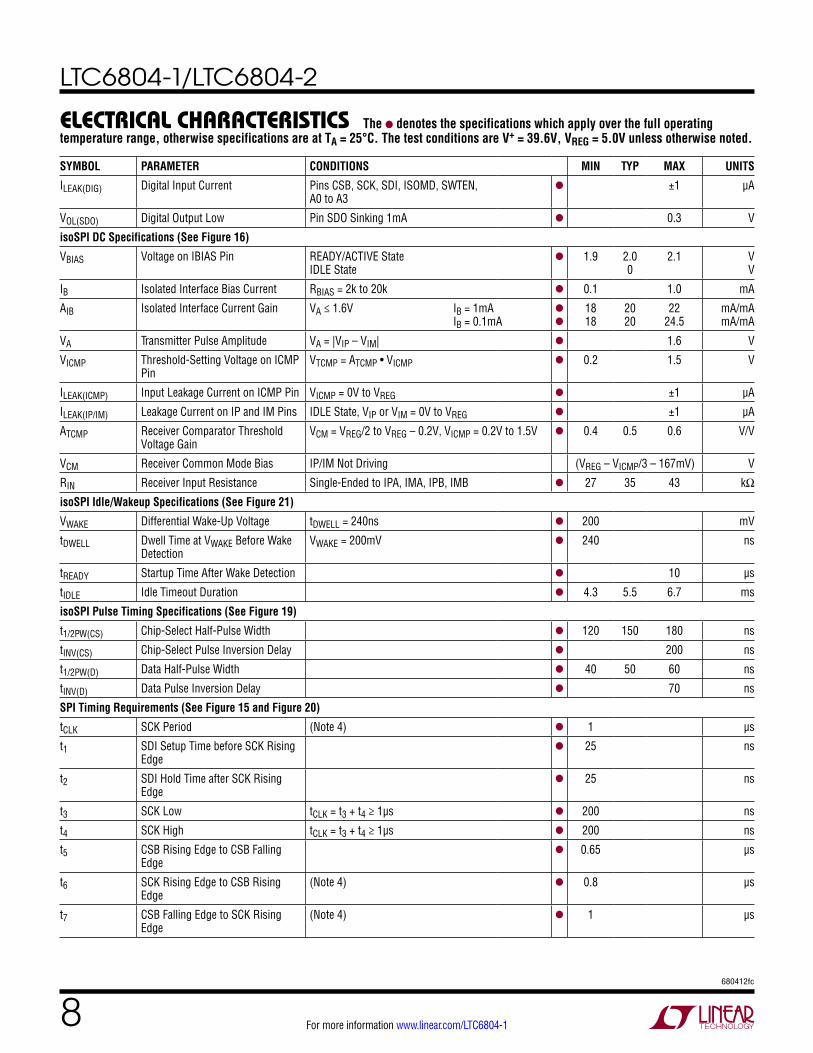
elecTrical characTerisTics
SYMBOL PARAMETER CONDITIONS MIN TYP MAX UNITS
V+ Supply Voltage TME Specifications Met (Note 6) l 11 40 55 V
VREG VREG Supply Voltage TME Supply Rejection < 1mV/V l 4.5 5 5.5 V
DRIVE output voltage Sourcing 1µA
l
5.4 5.2
5.6 5.6
5.8 6.0
V V
Sourcing 500µA l 5.1 5.6 6.1 V
VREGD Digital Supply Voltage l 2.7 3.0 3.6 V
Discharge Switch ON Resistance VCELL = 3.6V l 10 25 Ω
Thermal Shutdown Temperature 150 °C
VOL(WDT) Watchdog Timer Pin Low WDT Pin Sinking 4mA l 0.4 V
VOL(GPIO) General Purpose I/O Pin Low GPIO Pin Sinking 4mA (Used as Digital Output) l 0.4 V
ADC Timing Specifications
tCYCLE (Figure 3)
Measurement + Calibration Cycle Time When Starting from the REFUP State in Normal Mode
Measure 12 Cells l 2120 2335 2480 µs
Measure 2 Cells l 365 405 430 µs
Measure 12 Cells and 2 GPIO Inputs l 2845 3133 3325 µs
Measurement + Calibration Cycle Time When Starting from the REFUP State in Filtered Mode
Measure 12 Cells l 183 201.3 213.5 ms
Measure 2 Cells l 30.54 33.6 35.64 ms
Measure 12 Cells and 2 GPIO Inputs l 244 268.4 284.7 ms
Measurement + Calibration Cycle Time When Starting from the REFUP State in Fast Mode
Measure 12 Cells l 1010 1113 1185 µs
Measure 2 Cells l 180 201 215 µs
Measure 12 Cells and 2 GPIO Inputs l 1420 1564 1660 µs
tSKEW1 (Figure 6)
Skew Time. The Time Difference between C12 and GPIO2 Measurements, Command = ADCVAX
Fast Mode l 189 208 221 µs
Normal Mode l 493 543 576 µs
tSKEW2 (Figure 3)
Skew Time. The Time Difference between C12 and C0 Measurements, Command = ADCV
Fast Mode l 211 233 248 µs
Normal Mode l 609 670 711 µs
tWAKE Regulator Start-Up Time VREG Generated from Drive Pin (Figure 28) l 100 300 µs
tSLEEP Watchdog or Software Discharge Timer
SWTEN Pin = 0 or DCTO[3:0] = 0000 l 1.8 2 2.2 sec
SWTEN Pin = 1 and DCTO[3:0] ≠ 0000 0.5 120 min
tREFUP (Figure 1, Figures 3 to 7)
Reference Wake-Up Time State: Core = STANDBY l 2.7 3.5 4.4 ms
State: Core = REFUP l 0 ms
fS ADC Clock Frequency l 3.0 3.3 3.5 MHz
SPI Interface DC Specifications
VIH(SPI) SPI Pin Digital Input Voltage High Pins CSB, SCK, SDI l 2.3 V
VIL(SPI) SPI Pin Digital Input Voltage Low Pins CSB, SCK, SDI l 0.8 V
VIH(CFG) Configuration Pin Digital Input Voltage High
Pins ISOMD, SWTEN, GPIO1 to GPIO5, A0 to A3 l 2.7 V
VIL(CFG) Configuration Pin Digital Input Voltage Low
Pins ISOMD, SWTEN, GPIO1 to GPIO5, A0 to A3 l 1.2 V
The l denotes the specifications which apply over the full operating temperature range, otherwise specifications are at TA = 25°C. The test conditions are V+ = 39.6V, VREG = 5.0V unless otherwise noted.
LTC6804-1/LTC6804-2
8680412fc
For more information www.linear.com/LTC6804-1
elecTrical characTerisTics
SYMBOL PARAMETER CONDITIONS MIN TYP MAX UNITS
ILEAK(DIG) Digital Input Current Pins CSB, SCK, SDI, ISOMD, SWTEN, A0 to A3
l ±1 µA
VOL(SDO) Digital Output Low Pin SDO Sinking 1mA l 0.3 V
isoSPI DC Specifications (See Figure 16)
VBIAS Voltage on IBIAS Pin READY/ACTIVE State IDLE State
l 1.9 2.0 0
2.1 V V
IB Isolated Interface Bias Current RBIAS = 2k to 20k l 0.1 1.0 mA
AIB Isolated Interface Current Gain VA ≤ 1.6V IB = 1mA IB = 0.1mA
l
l
18 18
20 20
22 24.5
mA/mA mA/mA
VA Transmitter Pulse Amplitude VA = |VIP – VIM| l 1.6 V
VICMP Threshold-Setting Voltage on ICMP Pin
VTCMP = ATCMP • VICMP l 0.2 1.5 V
ILEAK(ICMP) Input Leakage Current on ICMP Pin VICMP = 0V to VREG l ±1 µA
ILEAK(IP/IM) Leakage Current on IP and IM Pins IDLE State, VIP or VIM = 0V to VREG l ±1 µA
ATCMP Receiver Comparator Threshold Voltage Gain
VCM = VREG/2 to VREG – 0.2V, VICMP = 0.2V to 1.5V l 0.4 0.5 0.6 V/V
VCM Receiver Common Mode Bias IP/IM Not Driving (VREG – VICMP/3 – 167mV) V
RIN Receiver Input Resistance Single-Ended to IPA, IMA, IPB, IMB l 27 35 43 kΩ
isoSPI Idle/Wakeup Specifications (See Figure 21)
VWAKE Differential Wake-Up Voltage tDWELL = 240ns l 200 mV
tDWELL Dwell Time at VWAKE Before Wake Detection
VWAKE = 200mV l 240 ns
tREADY Startup Time After Wake Detection l 10 µs
tIDLE Idle Timeout Duration l 4.3 5.5 6.7 ms
isoSPI Pulse Timing Specifications (See Figure 19)
t1/2PW(CS) Chip-Select Half-Pulse Width l 120 150 180 ns
tINV(CS) Chip-Select Pulse Inversion Delay l 200 ns
t1/2PW(D) Data Half-Pulse Width l 40 50 60 ns
tINV(D) Data Pulse Inversion Delay l 70 ns
SPI Timing Requirements (See Figure 15 and Figure 20)
tCLK SCK Period (Note 4) l 1 µs
t1 SDI Setup Time before SCK Rising Edge
l 25 ns
t2 SDI Hold Time after SCK Rising Edge
l 25 ns
t3 SCK Low tCLK = t3 + t4 ≥ 1µs l 200 ns
t4 SCK High tCLK = t3 + t4 ≥ 1µs l 200 ns
t5 CSB Rising Edge to CSB Falling Edge
l 0.65 µs
t6 SCK Rising Edge to CSB Rising Edge
(Note 4) l 0.8 µs
t7 CSB Falling Edge to SCK Rising Edge
(Note 4) l 1 µs
The l denotes the specifications which apply over the full operating temperature range, otherwise specifications are at TA = 25°C. The test conditions are V+ = 39.6V, VREG = 5.0V unless otherwise noted.
LTC6804-1/LTC6804-2
9680412fc
For more information www.linear.com/LTC6804-1
elecTrical characTerisTics
SYMBOL PARAMETER CONDITIONS MIN TYP MAX UNITS
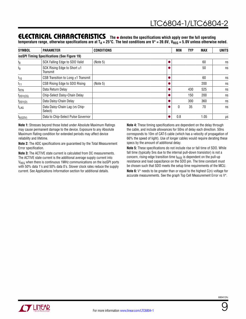
isoSPI Timing Specifications (See Figure 19)
t8 SCK Falling Edge to SDO Valid (Note 5) l 60 ns
t9 SCK Rising Edge to Short ±1 Transmit
l 50 ns
t10 CSB Transition to Long ±1 Transmit l 60 ns
t11 CSB Rising Edge to SDO Rising (Note 5) l 200 ns
tRTN Data Return Delay l 430 525 ns
tDSY(CS) Chip-Select Daisy-Chain Delay l 150 200 ns
tDSY(D) Data Daisy-Chain Delay l 300 360 ns
tLAG Data Daisy-Chain Lag (vs Chip-Select)
l 0 35 70 ns
t6(GOV) Data to Chip-Select Pulse Governor l 0.8 1.05 µs
The l denotes the specifications which apply over the full operating temperature range, otherwise specifications are at TA = 25°C. The test conditions are V+ = 39.6V, VREG = 5.0V unless otherwise noted.
Note 1: Stresses beyond those listed under Absolute Maximum Ratings may cause permanent damage to the device. Exposure to any Absolute Maximum Rating condition for extended periods may affect device reliability and lifetime.Note 2: The ADC specifications are guaranteed by the Total Measurement Error specification.Note 3: The ACTIVE state current is calculated from DC measurements. The ACTIVE state current is the additional average supply current into VREG when there is continuous 1MHz communications on the isoSPI ports with 50% data 1’s and 50% data 0’s. Slower clock rates reduce the supply current. See Applications Information section for additional details.
Note 4: These timing specifications are dependent on the delay through the cable, and include allowances for 50ns of delay each direction. 50ns corresponds to 10m of CAT-5 cable (which has a velocity of propagation of 66% the speed of light). Use of longer cables would require derating these specs by the amount of additional delay.Note 5: These specifications do not include rise or fall time of SDO. While fall time (typically 5ns due to the internal pull-down transistor) is not a concern, rising-edge transition time tRISE is dependent on the pull-up resistance and load capacitance on the SDO pin. The time constant must be chosen such that SDO meets the setup time requirements of the MCU.Note 6: V+ needs to be greater than or equal to the highest C(n) voltage for accurate measurements. See the graph Top Cell Measurement Error vs V+.
LTC6804-1/LTC6804-2
10680412fc
For more information www.linear.com/LTC6804-1
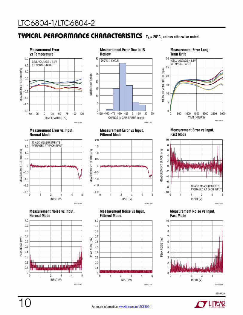
Measurement Error vs Input, Normal Mode
Measurement Error vs Input, Filtered Mode
Measurement Error vs Input, Fast Mode
Measurement Error vs Temperature
Measurement Error Due to IR Reflow
Measurement Error Long- Term Drift
Typical perForMance characTerisTics
Measurement Noise vs Input, Normal Mode
Measurement Noise vs Input, Filtered Mode
Measurement Noise vs Input, Fast Mode
TA = 25°C, unless otherwise noted.
TEMPERATURE (°C)–50
MEA
SURE
MEN
T ER
ROR
(mV)
1.5
25
680412 G01
0
–1.0
–25 0 50
–1.5
–2.0
2.0
1.0
0.5
–0.5
75 100 125
CELL VOLTAGE = 3.3V5 TYPICAL UNITS
CHANGE IN GAIN ERROR (ppm)–125
NUM
BER
OF P
ARTS
20
25
30
25 50 75–50 –25 0
680412 G02
15
10
–100 –75
5
0
35260°C, 1 CYCLE
TIME (HOURS)0
MEA
SURE
MEN
T ER
ROR
(ppm
)
30
5
25
15
20
10
0
680412 G03
30001000 2000 2500500 1500
CELL VOLTAGE = 3.3V8 TYPICAL PARTS
INPUT (V)0
MEA
SURE
MEN
T ER
ROR
(mV)
–0.5
0
0.5
3 5
680412 G04
–1.0
–1.5
–2.01 2 4
1.0
1.5
2.010 ADC MEASUREMENTSAVERAGED AT EACH INPUT
INPUT (V)0
MEA
SURE
MEN
T ER
ROR
(mV)
–0.5
0
0.5
3 5
680412 G05
–1.0
–1.5
–2.01 2 4
1.0
1.5
2.0
INPUT (V)0
MEA
SURE
MEN
T ER
ROR
(mV)
2
6
10
4
680412 G06
–2
–6
0
4
8
–4
–8
–101 2 3 5
10 ADC MEASUREMENTSAVERAGED AT EACH INPUT
INPUT (V)0
PEAK
NOI
SE (m
V)
0.6
0.8
1.0
4
680412 G07
0.4
0.2
0.5
0.7
0.9
0.3
0.1
01 2 3 5
INPUT (V)0
PEAK
NOI
SE (m
V)
0.6
0.8
1.0
4
680412 G08
0.4
0.2
0.5
0.7
0.9
0.3
0.1
01 2 3 5
INPUT (V)0
PEAK
NOI
SE (m
V)
6
8
10
4
680412 G09
4
2
5
7
9
3
1
01 2 3
LTC6804-1/LTC6804-2
11680412fc
For more information www.linear.com/LTC6804-1
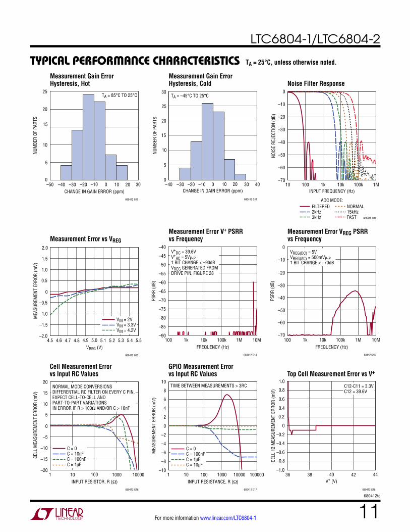
Typical perForMance characTerisTicsMeasurement Gain Error Hysteresis, Hot
Measurement Gain Error Hysteresis, Cold Noise Filter Response
Measurement Error vs VREG
Measurement Error V+ PSRR vs Frequency
Measurement Error VREG PSRR vs Frequency
TA = 25°C, unless otherwise noted.
CHANGE IN GAIN ERROR (ppm)–50
NUM
BER
OF P
ARTS
15
20
25TA = 85°C TO 25°C
–20 0 30
680412 G10
10
5
0–40 –30 –10 10 20
CHANGE IN GAIN ERROR (ppm)–40
0
NUM
BER
OF P
ARTS
5
10
15
20
–20 0 20 40
680412 G11
25
30TA = –45°C TO 25°C
–30 –10 10 30INPUT FREQUENCY (Hz)
10
NOIS
E RE
JECT
ION
(dB)
0
–50
–10
–30
–20
–40
–70
–60
680412 G12
1M1k 100k100 10k
FILTERED2kHz3kHz
ADC MODE:NORMAL15kHzFAST
VREG (V)4.5
MEA
SURE
MEN
T ER
ROR
(mV)
0
0.5
1.0
5.3 5.4
680412 G13
–0.5
–1.0
–2.04.7 4.9 5.14.6 5.54.8 5.0 5.2
–1.5
2.0
1.5
VIN = 2VVIN = 3.3VVIN = 4.2V
FREQUENCY (Hz)100
PSRR
(dB) –60
–50
–40
1M
680412 G14
–70
–80
–65
–55
–45
–75
–85
–901k 10k 100k 10M
V+DC = 39.6V
V+AC = 5VP-P
1 BIT CHANGE < –90dBVREG GENERATED FROMDRIVE PIN, FIGURE 28
FREQUENCY (Hz)100
–20
–10
0
1M
68412 G15
–30
–40
1k 10k 100k 10M
–50
–60
–70
PSRR
(dB)
VREG(DC) = 5VVREG(AC) = 500mVP-P1 BIT CHANGE < –70dB
Cell Measurement Error vs Input RC Values
GPIO Measurement Error vs Input RC Values Top Cell Measurement Error vs V+
INPUT RESISTOR, R (Ω)1
CELL
MEA
SURE
MEN
T ER
ROR
(mV)
0
5
10
10000
680412 G16
–5
–10
–2010 100 1000
–15
20NORMAL MODE CONVERSIONSDIFFERENTIAL RC FILTER ON EVERY C PIN.EXPECT CELL-TO-CELL AND PART-TO-PART VARIATIONSIN ERROR IF R > 100Ω AND/OR C > 10nF
15
C = 0C = 10nFC = 100nFC = 1µF
INPUT RESISTANCE, R (Ω)1
MEA
SURE
MEN
T ER
ROR
(mV)
2
6
10
10000
680412 G17
–2
–6
0
4
8
–4
–8
–1010 100 1000 100000
C = 0C = 100nFC = 1µFC = 10µF
TIME BETWEEN MEASUREMENTS > 3RC
V+ (V)36
–1.0
CELL
12
MEA
SURE
MEN
T ER
ROR
(mV)
–0.8
–0.4
–0.2
0
1.0
0.4
38 40
680412 G18
–0.6
0.6
0.8
0.2
42 44
C12-C11 = 3.3VC12 = 39.6V
LTC6804-1/LTC6804-2
12680412fc
For more information www.linear.com/LTC6804-1
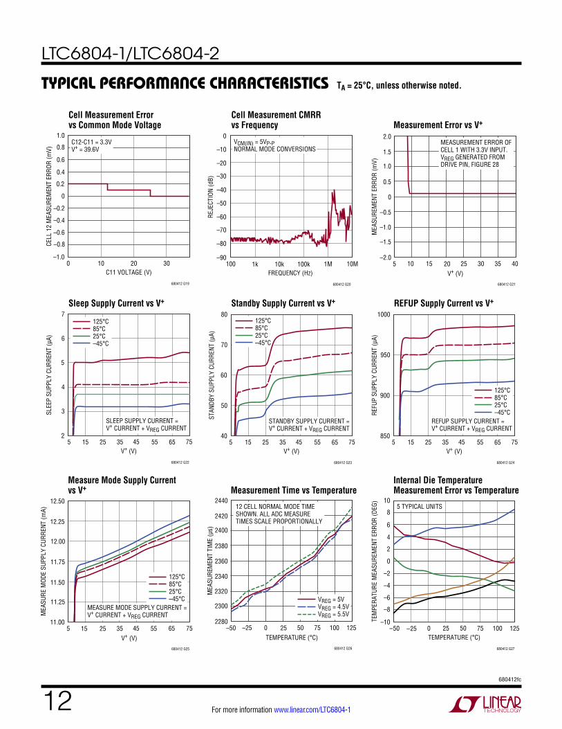
Typical perForMance characTerisTics
Cell Measurement Error vs Common Mode Voltage
Cell Measurement CMRR vs Frequency Measurement Error vs V+
Sleep Supply Current vs V+ Standby Supply Current vs V+ REFUP Supply Current vs V+
TA = 25°C, unless otherwise noted.
C11 VOLTAGE (V)0
–1.0
CELL
12
MEA
SURE
MEN
T ER
ROR
(mV)
–0.8
–0.4
–0.2
0
1.0
0.4
10 20
680412 G19
–0.6
0.6
0.8
0.2
30
C12-C11 = 3.3VV+ = 39.6V
FREQUENCY (Hz)100
–90
REJE
CTIO
N (d
B)
–80
–60
–50
–40
10k 1M 10M
0
680412 G20
–70
1k 100k
–30
–20
–10VCM(IN) = 5VP-PNORMAL MODE CONVERSIONS
V+ (V)5
MEA
SURE
MEN
T ER
ROR
(mV)
1.5
20
680412 G21
0
–1.0
10 15 25
–1.5
–2.0
2.0
1.0
0.5
–0.5
30 35 40
MEASUREMENT ERROR OFCELL 1 WITH 3.3V INPUT.VREG GENERATED FROMDRIVE PIN, FIGURE 28
V+ (V)5 15
2
SLEE
P SU
PPLY
CUR
RENT
(µA)
4
7
25 45 55
680412 G22
3
6
5
35 65 75
125°C85°C25°C–45°C
SLEEP SUPPLY CURRENT = V+ CURRENT + VREG CURRENT
V+ (V)155
40
STAN
DBY
SUPP
LY C
URRE
NT (µ
A)
50
80
25 45 55
680412 G23
70
60
35 65 75
125°C85°C25°C–45°C
STANDBY SUPPLY CURRENT = V+ CURRENT + VREG CURRENT
V+ (V)155
850
REFU
P SU
PPLY
CUR
RENT
(µA)
1000
25 45 55
680412 G24
950
900
35 65 75
125°C85°C25°C–45°C
REFUP SUPPLY CURRENT = V+ CURRENT + VREG CURRENT
Measure Mode Supply Current vs V+ Measurement Time vs Temperature
Internal Die Temperature Measurement Error vs Temperature
V+ (V)5
MEA
SURE
MOD
E SU
PPLY
CUR
RENT
(mA)
12.00
12.25
12.50
35 55
680412 G25
11.75
11.50
15 25 45 65 75
11.25
11.00
125°C85°C25°C–45°C
MEASURE MODE SUPPLY CURRENT = V+ CURRENT + VREG CURRENT
TEMPERATURE (°C)–50
MEA
SURE
MEN
T TI
ME
(µs)
2420
25
680412 G26
2360
2320
–25 0 50
2300
2280
2440
2400
2380
2340
75 100 125
VREG = 5VVREG = 4.5VVREG = 5.5V
12 CELL NORMAL MODE TIMESHOWN. ALL ADC MEASURETIMES SCALE PROPORTIONALLY
TEMPERATURE (°C)–50
–10TEM
PERA
TURE
MEA
SURE
MEN
T ER
ROR
(DEG
)
–8
–4
–2
0
10
4
0 50 75 100
680412 G27
–6
6
8
2
–25 25 125
5 TYPICAL UNITS
LTC6804-1/LTC6804-2
13680412fc
For more information www.linear.com/LTC6804-1
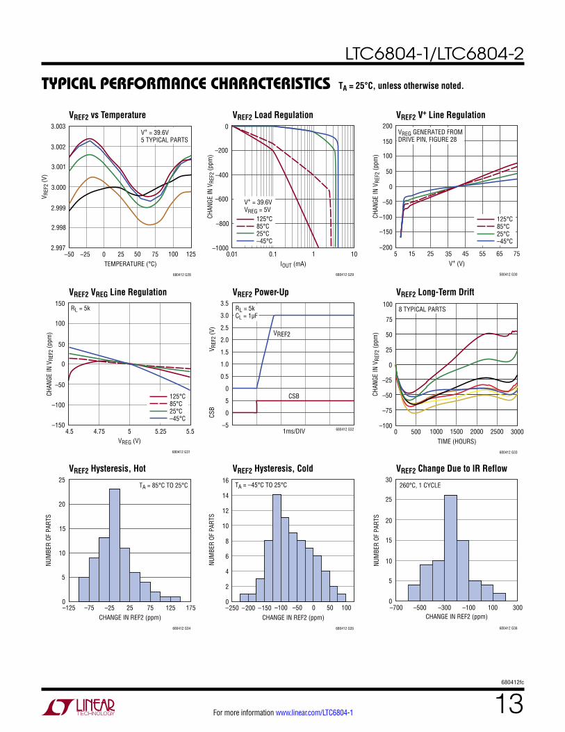
Typical perForMance characTerisTics
VREF2 vs Temperature VREF2 Load Regulation VREF2 V+ Line Regulation
VREF2 VREG Line Regulation
VREF2 Hysteresis, Hot
VREF2 Power-Up
VREF2 Hysteresis, Cold
VREF2 Long-Term Drift
VREF2 Change Due to IR Reflow
TA = 25°C, unless otherwise noted.
TEMPERATURE (°C)–50
V REF
2 (V
)
3.001
3.002
3.003
25 75
680412 G28
3.000
2.999
–25 0 50 100 125
2.998
2.997
V+ = 39.6V5 TYPICAL PARTS
IOUT (mA)0.01
CHAN
GE IN
VRE
F2 (p
pm)
–600
–400
680412 G29
–800
–10000.1 1 10
0
–200
125°C85°C25°C–45°C
V+ = 39.6VVREG = 5V
V+ (V)5
CHAN
GE IN
VRE
F2 (p
pm)
150
35
580412 G30
0
–100
15 25 45
–150
–200
200
100
50
–50
55 65 75
125°C85°C25°C–45°C
VREG GENERATED FROMDRIVE PIN, FIGURE 28
VREG (V)4.5
–150
CHAN
GE IN
VRE
F2 (p
pm)
–100
–50
0
50
100
150RL = 5k
4.75 5 5.25 5.5
680412 G31
125°C85°C25°C–45°C
V REF
2 (V
)CS
B
1.5
2.5
3.5
680412 G32
0.5
5
1.0
2.0
3.0
0
0
–51ms/DIV
VREF2
CSB
RL = 5kCL = 1µF
TIME (HOURS)0
CHAN
GE IN
VRE
F2 (p
pm)
0
680412 G33
–50
–1001000 2000500 1500 2500
50
100
–25
–75
25
75
3000
8 TYPICAL PARTS
CHANGE IN REF2 (ppm)–125
NUM
BER
OF P
ARTS
15
20
25TA = 85°C TO 25°C
75
680412 G34
10
5
0–75 –25 25 125 175
CHANGE IN REF2 (ppm)–250
NUM
BER
OF P
ARTS
8
12
680412 G35
4
0–200 –150 –100 –50 0 50 100
16
6
10
2
14
TA = –45°C TO 25°C
CHANGE IN REF2 (ppm)
0
NUM
BER
OF P
ARTS
10
20
30260°C, 1 CYCLE
5
15
25
–500 –300 –100 100
680412 G36
300–700
LTC6804-1/LTC6804-2
14680412fc
For more information www.linear.com/LTC6804-1
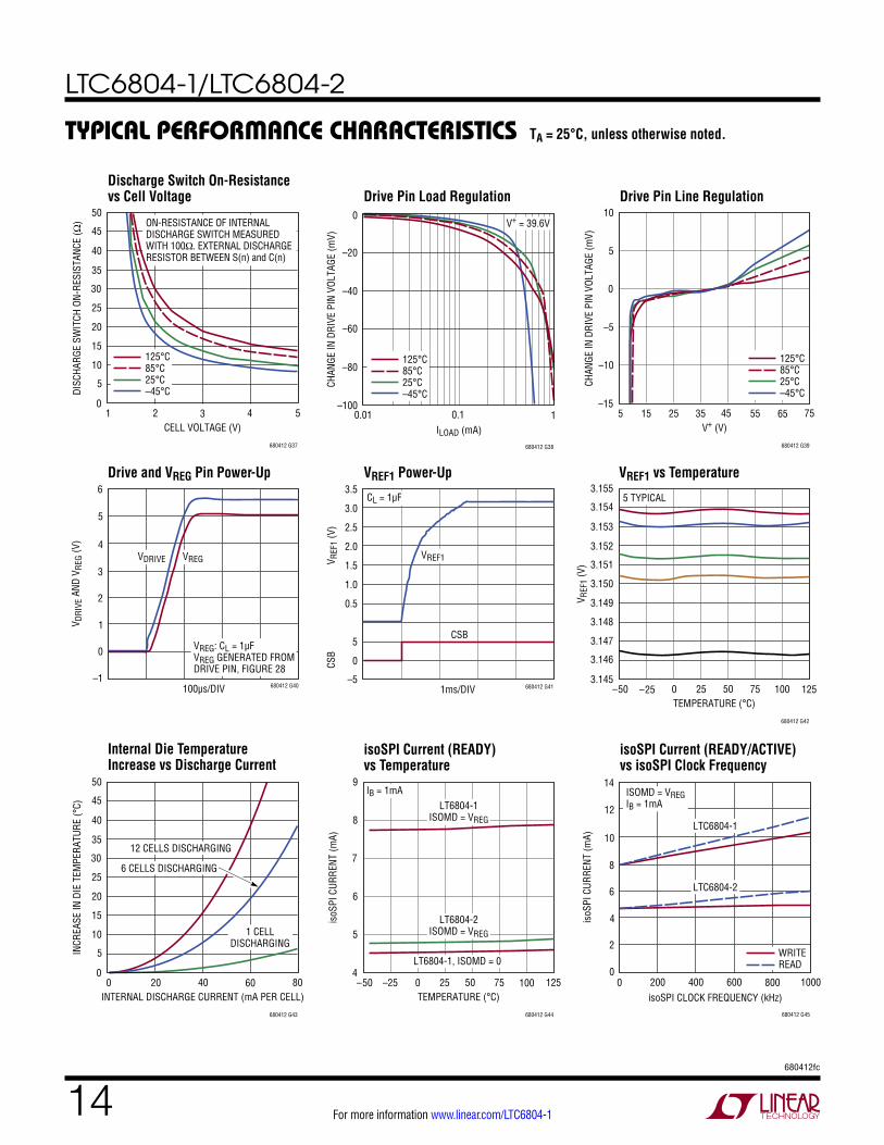
Typical perForMance characTerisTics
Drive and VREG Pin Power-Up VREF1 Power-Up VREF1 vs Temperature
Internal Die Temperature Increase vs Discharge Current
isoSPI Current (READY) vs Temperature
isoSPI Current (READY/ACTIVE) vs isoSPI Clock Frequency
Discharge Switch On-Resistance vs Cell Voltage Drive Pin Load Regulation Drive Pin Line Regulation
TA = 25°C, unless otherwise noted.
CELL VOLTAGE (V)
0
DISC
HARG
E SW
ITCH
ON-
RESI
STAN
CE (Ω
)
5
15
20
25
50
35
1 2
680412 G37
10
40
45
30
3 4 5
125°C85°C25°C–45°C
ON-RESISTANCE OF INTERNALDISCHARGE SWITCH MEASUREDWITH 100Ω. EXTERNAL DISCHARGERESISTOR BETWEEN S(n) and C(n)
ILOAD (mA)0.01
CHAN
GE IN
DRI
VE P
IN V
OLTA
GE (m
V)–60
–40
1
680412 G38
–80
–1000.1
0
–20
125°C85°C25°C–45°C
V+ = 39.6V
V+ (V)5 15
–15
CHAN
GE IN
DRI
VE P
IN V
OLTA
GE (m
V)
–5
10
25 45 55
680412 G39
–10
5
0
35 65 75
125°C85°C25°C–45°C
4
5
6
680412 G40
3
2
100µs/DIV
1
0
–1
V DRI
VE A
ND V
REG
(V)
VDRIVE VREG
VREG: CL = 1µFVREG GENERATED FROMDRIVE PIN, FIGURE 28
V REF
1 (V
)CS
B
1.5
2.5
3.5
680412 G41
0.5
5
–5
1.0
2.0
3.0
CSB
0
1ms/DIV
VREF1
CL = 1µF
TEMPERATURE (°C)–50
3.145
V REF
1 (V
)
3.146
3.148
3.149
3.150
3.155
3.152
0 50 75 100
680412 G42
3.147
3.153
3.154
3.151
–25 25 125
5 TYPICAL
INTERNAL DISCHARGE CURRENT (mA PER CELL)0
0
INCR
EASE
IN D
IE T
EMPE
RATU
RE (°
C)
5
15
20
25
50
35
20 40
680412 G43
10
40
45
30
60 80
12 CELLS DISCHARGING
1 CELLDISCHARGING
6 CELLS DISCHARGING
isoSPI CLOCK FREQUENCY (kHz)0
10
12
14
800
680412 G45
8
6
200 400 600 1000
4
2
0
isoS
PI C
URRE
NT (m
A)
WRITEREAD
LTC6804-1
LTC6804-2
ISOMD = VREGIB = 1mA
TEMPERATURE (°C)–50 –25
4
isoS
PI C
URRE
NT (m
A)
6
9
0 50 75
680412 G44
5
8
7
25 100 125
IB = 1mALT6804-1
ISOMD = VREG
LT6804-2ISOMD = VREG
LT6804-1, ISOMD = 0
LTC6804-1/LTC6804-2
15680412fc
For more information www.linear.com/LTC6804-1
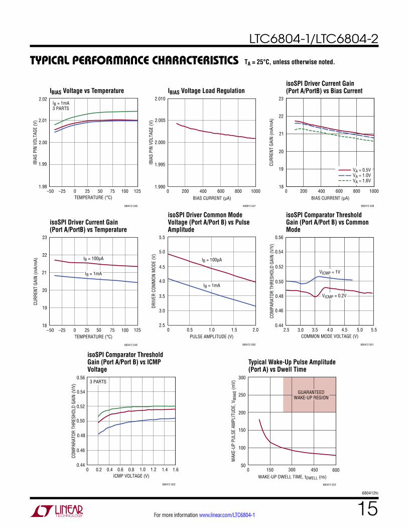
Typical perForMance characTerisTics
isoSPI Driver Current Gain (Port A/PortB) vs Temperature
isoSPI Driver Common Mode Voltage (Port A/Port B) vs Pulse Amplitude
isoSPI Comparator Threshold Gain (Port A/Port B) vs Common Mode
isoSPI Comparator Threshold Gain (Port A/Port B) vs ICMP Voltage
Typical Wake-Up Pulse Amplitude (Port A) vs Dwell Time
IBIAS Voltage vs Temperature IBIAS Voltage Load RegulationisoSPI Driver Current Gain (Port A/PortB) vs Bias Current
TA = 25°C, unless otherwise noted.
TEMPERATURE (°C)–50
1.98
IBIA
S PI
N VO
LTAG
E (V
)
1.99
2.00
2.01
2.02
–25 0 25 50
680412 G46
75 100 125
IB = 1mA3 PARTS
BIAS CURRENT (µA)0
IBIA
S PI
N VO
LTAG
E (V
)
2.000
2.005
800
408912 G47
1.995
1.990200 400 600 1000
2.010
BIAS CURRENT (µA)0
CURR
ENT
GAIN
(mA/
mA)
21
22
23
800
680412 G48
20
19
18200 400 600 1000
VA = 0.5VVA = 1.0VVA = 1.6V
TEMPERATURE (°C)–50 –25
18
CURR
ENT
GAIN
(mA/
mA)
20
23
0 50 75
680412 G49
19
22
21
25 100 125
IB = 100µA
IB = 1mA
PULSE AMPLITUDE (V)0
2.5
DRIV
ER C
OMM
ON M
ODE
(V)
3.0
3.5
4.0
4.5
5.0
5.5
0.5 1.0 1.5 2.0
IB = 100µA
IB = 1mA
680412 G50
COMMON MODE VOLTAGE (V)2.5
0.44
COM
PARA
TOR
THRE
SHOL
D GA
IN (V
/V)
0.46
0.48
0.50
0.52
0.56
3.0 3.5 4.0 4.5
680412 G51
5.0 5.5
0.54
VICMP = 1V
VICMP = 0.2V
ICMP VOLTAGE (V)0
0.44
COM
PARA
TOR
THRE
SHOL
D GA
IN (V
/V)
0.46
0.48
0.50
0.52
0.4 0.8 1.2 1.6
680412 G52
0.54
0.56
0.2 0.6 1.0 1.4
3 PARTS
WAKE-UP DWELL TIME, tDWELL (ns)0
WAK
E-UP
PUL
SE A
MPL
ITUD
E, V
WAK
E (m
V)
150
200
600
680412 G53
100
50150 300 450
300
250 GUARANTEEDWAKE-UP REGION
LTC6804-1/LTC6804-2
16680412fc
For more information www.linear.com/LTC6804-1
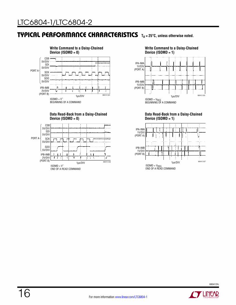
Typical perForMance characTerisTics TA = 25°C, unless otherwise noted.
Write Command to a Daisy-Chained Device (ISOMD = 0)
Data Read-Back from a Daisy-Chained Device (ISOMD = 0)
Write Command to a Daisy-Chained Device (ISOMD = 1)
Data Read-Back from a Daisy-Chained Device (ISOMD = 1)
CSB5V/DIV
SDI5V/DIV
SCK5V/DIV
SDO5V/DIV
IPB-IMB2V/DIV
(PORT B)1µs/DIV 680412 G54
ISOMD = V–
BEGINNING OF A COMMAND
PORT A
IPB-IMB1V/DIV
(PORT B)
IPA-IMA1V/DIV
(PORT A)
1µs/DIV 680412 G55
ISOMD = VREGBEGINNING OF A COMMAND
CSB5V/DIV
SDI5V/DIV
SCK5V/DIV
SDO5V/DIV
IPB-IMB2V/DIV
(PORT B)
PORT A
1µs/DIV 680412 G56
ISOMD = V–
END OF A READ COMMAND
IPB-IMB1V/DIV
(PORT B)
IPA-IMA1V/DIV
(PORT A)
1µs/DIV 680412 G57
ISOMD = VREGEND OF A READ COMMAND
LTC6804-1/LTC6804-2
17680412fc
For more information www.linear.com/LTC6804-1
pin FuncTionsC0 to C12: Cell Inputs.
S1 to S12: Balance Inputs/Outputs. 12 N-MOSFETs are connected between S(n) and C(n – 1) for discharging cells.
V+: Positive Supply Pin.
V–: Negative Supply Pins. The V– pins must be shorted together, external to the IC.
VREF2: Buffered 2nd reference voltage for driving multiple 10k thermistors. Bypass with an external 1µF capacitor.
VREF1: ADC Reference Voltage. Bypass with an external 1µF capacitor. No DC loads allowed.
GPIO[1:5]: General Purpose I/O. Can be used as digital inputs or digital outputs, or as analog inputs with a mea-surement range from V– to 5V. GPIO [3:5] can be used as an I2C or SPI port.
SWTEN: Software Timer Enable. Connect this pin to VREG to enable the software timer.
DRIVE: Connect the base of an NPN to this pin. Connect the collector to V+ and the emitter to VREG.
VREG: 5V Regulator Input. Bypass with an external 1µF capacitor.
ISOMD: Serial Interface Mode. Connecting ISOMD to VREG configures Pins 41 to 44 of the LTC6804 for 2-wire isolated interface (isoSPI) mode. Connecting ISOMD to V– configures the LTC6804 for 4-wire SPI mode.
WDT: Watchdog Timer Output Pin. This is an open drain NMOS digital output. It can be left unconnected or con-nected with a 1M resistor to VREG. If the LTC6804 does not receive a wake-up signal (see Figure 21) within 2 seconds, the watchdog timer circuit will reset the LTC6804 and the WDT pin will go high impedance.
Serial Port PinsLTC6804-1
(DAISY-CHAINABLE)LTC6804-2
(ADDRESSABLE)
ISOMD = VREG ISOMD = V– ISOMD = VREG ISOMD = V–
PORT B (Pins 45 to 48)
IPB IPB A3 A3
IMB IMB A2 A2
ICMP ICMP A1 A1
IBIAS IBIAS A0 A0
PORT A (Pins 41 to 44)
(NC) SDO IBIAS SDO
(NC) SDI ICMP SDI
IPA SCK IPA SCK
IMA CSB IMA CSB
CSB, SCK, SDI, SDO: 4-Wire Serial Peripheral Interface (SPI). Active low chip select (CSB), serial clock (SCK), and serial data in (SDI) are digital inputs. Serial data out (SDO) is an open drain NMOS output pin. SDO requires a 5k pull-up resistor.
A0 to A3: Address Pins. These digital inputs are connected to VREG or V– to set the chip address for addressable se-rial commands.
IPA, IMA: Isolated 2-Wire Serial Interface Port A. IPA (plus) and IMA (minus) are a differential input/output pair.
IPB, IMB: Isolated 2-Wire Serial Interface Port B. IPB (plus) and IMB (minus) are a differential input/output pair.
IBIAS: Isolated Interface Current Bias. Tie IBIAS to V– through a resistor divider to set the interface output current level. When the isoSPI interface is enabled, the IBIAS pin voltage is 2V. The IPA/IMA or IPB/IMB output current drive is set to 20 times the current, IB, sourced from the IBIAS pin.
ICMP: Isolated Interface Comparator Voltage Threshold Set. Tie this pin to the resistor divider between IBIAS and V– to set the voltage threshold of the isoSPI receiver comparators. The comparator thresholds are set to 1/2 the voltage on the ICMP pin.
LTC6804-1/LTC6804-2
18680412fc
For more information www.linear.com/LTC6804-1
block DiagraM
C12C11C10C9C8C7
C0
C6
C5C4C3C2C1
–
+
680412 BD1
IPB
P
IMB
ICMP
IBIAS
SDO/(NC)
SDI/(NC)
SCK/(IPA)
CSB/(IMA)
ISOMD
WDT
DRIVE
VREG
SWTEN
VREF1
VREF2
GPIO5
GPIO4
V–
V–*
GPIO3
GPIO2
GPIO1
C0
S1
V+
C12
S12
C11
M
S11
C10
S10
C9
S9
C8
S8
C7
S7
C6
S6
C5
S5
C4
S4
C3
S3
C2
S2
C1
LOGICAND
MEMORY
DIGITALFILTERS
SERIAL I/OPORT B
6-CELLMUX
VREGDSOCVREG
P
M
AUXMUX
12 BALANCE FETsS(n)
C(n – 1)
P
M
6-CELLMUX
PORVREGD VREG
SERIAL I/OPORT A
SOFTWARETIMER
DIETEMPERATURE
2NDREFERENCE
1STREFERENCE
REGULATORS
ADC2
–
+ADC1
16
16
V+
LDO1 VREGDPOR
V+
LDO2DRIVE
48
47
46
45
44
43
42
41
40
39
38
37
36
35
34
33
32
31
30
29
28
27
26
25
1
2
3
4
5
6
7
8
9
10
11
12
13
14
15
16
17
18
19
20
21
22
23
24
LTC6804-1
LTC6804-1/LTC6804-2
19680412fc
For more information www.linear.com/LTC6804-1
block DiagraM
SDO/(IBIAS)
C12C11C10C9C8C7
C0
C6
C5C4C3C2C1
–
+
680412 BD2
A4
P
A3
A2
A1
SDI/(ICMP)
SCK/(IPA)
CSB/(IMA)
ISOMD
WDT
DRIVE
SWTEN
GPIO5
GPIO4
GPIO3
GPIO2
GPIO1
C0
S1
C12
S12
C11
M
S11
C10
S10
C9
S9
C8
S8
C7
S7
C6
S6
C5
S5
C4
S4
C3
S3
C2
S2
C1
LOGICAND
MEMORY
DIGITALFILTERS
SERIAL I/OADDRESS
6-CELLMUX
VREGDSOCVREG
P
M
AUXMUX
P
M
6-CELLMUX
PORVREGD VREG
SERIAL I/OPORT A
SOFTWARETIMER
DIETEMPERATURE
2NDREFERENCE
1STREFERENCE
REGULATORS
ADC2
–
+ADC1
V+
LDO1 VREGDPOR
V+
LDO2DRIVE
VREG
VREF1
VREF2
V–
V–*
V+
48
47
46
45
44
43
42
41
40
39
38
37
36
35
34
33
32
31
30
29
28
27
26
25
1
2
3
4
5
6
7
8
9
10
11
12
13
14
15
16
17
18
19
20
21
22
23
24
16
16
12 BALANCE FETsS(n)
C(n – 1)
LTC6804-2
LTC6804-1/LTC6804-2
20680412fc
For more information www.linear.com/LTC6804-1
operaTionSTATE DIAGRAM
The operation of the LTC6804 is divided into two separate sections: the core circuit and the isoSPI circuit. Both sec-tions have an independent set of operating states, as well as a shutdown timeout.
LTC6804 CORE STATE DESCRIPTIONS
SLEEP State
The reference and ADCs are powered down. The watchdog timer (see Watchdog and Software Discharge Timer) has timed out. The software discharge timer is either disabled or timed out. The supply currents are reduced to minimum levels. The isoSPI ports will be in the IDLE state.
If a WAKEUP signal is received (see Waking Up the Serial Interface), the LTC6804 will enter the STANDBY state.
STANDBY State
The reference and the ADCs are off. The watchdog timer and/or the software discharge timer is running. The DRIVE pin powers the VREG pin to 5V through an external transistor. (Alternatively, VREG can be powered by an external supply).
When a valid ADC command is received or the REFON bit is set to 1 in the Configuration Register Group, the IC pauses for tREFUP to allow for the reference to power up and then enters either the REFUP or MEASURE state. If there is no WAKEUP signal for a duration tSLEEP (when both the watch-dog and software discharge timer have expired) the LTC6804
Figure 1. LTC6804 Operation State Diagram
returns to the SLEEP state. If the software discharge timer is disabled, only the watchdog timer is relevant.
REFUP State
To reach this state the REFON bit in the Configuration Reg-ister Group must be set to 1 (using the WRCFG command, see Table 36). The ADCs are off. The reference is powered up so that the LTC6804 can initiate ADC conversions more quickly than from the STANDBY state.
When a valid ADC command is received, the IC goes to the MEASURE state to begin the conversion. Otherwise, the LTC6804 will return to the STANDBY state when the REFON bit is set to 0, either manually (using WRCFG command) or automatically when the watchdog timer expires. (The LTC6804 will then move straight into the SLEEP state if both timers are expired).
MEASURE State
The LTC6804 performs ADC conversions in this state. The reference and ADCs are powered up.
After ADC conversions are complete the LTC6804 will transition to either the REFUP or STANDBY states, de-pending on the REFON bit. Additional ADC conversions can be initiated more quickly by setting REFON = 1 to take advantage of the REFUP state.
Note: Non-ADC commands do not cause a Core state tran-sition. Only an ADC conversion or diagnostic commands will place the Core in the MEASURE state.
680412 F01
isoSPI PORTCORE LTC6804
CONVERSION DONE(REFON = 1)
WAKEUPSIGNAL(tWAKE)
ADC COMMAND(tREFUP)
ADCCOMMAND
REFON = 1(tREFUP)
WAKEUP SIGNAL(CORE = STANDBY)(tREADY)
WAKEUP SIGNAL(CORE = SLEEP)(tWAKE)
TRANSMIT/RECEIVE
NOTE: STATE TRANSITIONDELAYS DENOTED BY (tX)
NO ACTIVITY ONisoSPI PORT
IDLE TIMEOUT(tIDLE)
CONVERSIONDONE (REFON = 0)
REFON = 0
WD TIMEOUTOR SWT TIMEOUT
(tSLEEP)
MEASUREREFUP
STANDBY
SLEEP
ACTIVE
READY
IDLE
LTC6804-1/LTC6804-2
21680412fc
For more information www.linear.com/LTC6804-1
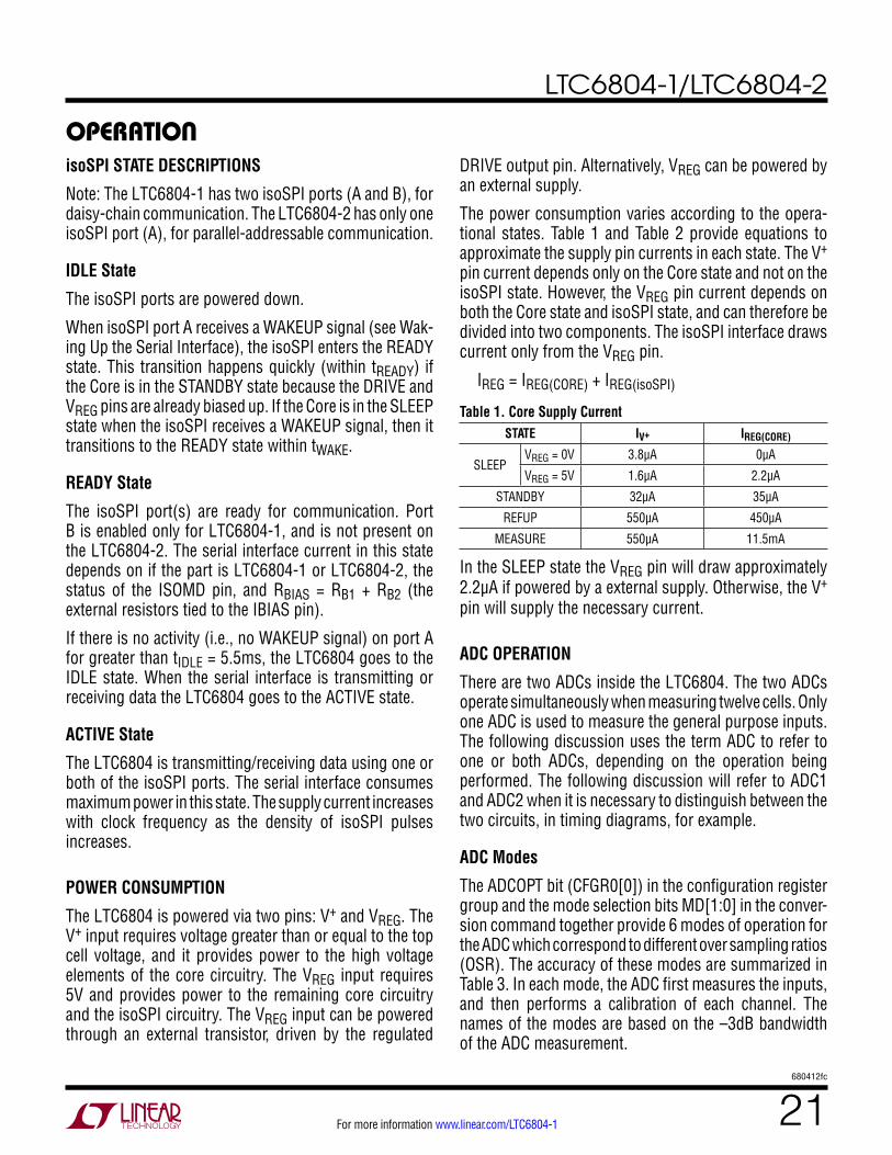
operaTionisoSPI STATE DESCRIPTIONS
Note: The LTC6804-1 has two isoSPI ports (A and B), for daisy-chain communication. The LTC6804-2 has only one isoSPI port (A), for parallel-addressable communication.
IDLE State
The isoSPI ports are powered down.
When isoSPI port A receives a WAKEUP signal (see Wak-ing Up the Serial Interface), the isoSPI enters the READY state. This transition happens quickly (within tREADY) if the Core is in the STANDBY state because the DRIVE and VREG pins are already biased up. If the Core is in the SLEEP state when the isoSPI receives a WAKEUP signal, then it transitions to the READY state within tWAKE.
READY State
The isoSPI port(s) are ready for communication. Port B is enabled only for LTC6804-1, and is not present on the LTC6804-2. The serial interface current in this state depends on if the part is LTC6804-1 or LTC6804-2, the status of the ISOMD pin, and RBIAS = RB1 + RB2 (the external resistors tied to the IBIAS pin).
If there is no activity (i.e., no WAKEUP signal) on port A for greater than tIDLE = 5.5ms, the LTC6804 goes to the IDLE state. When the serial interface is transmitting or receiving data the LTC6804 goes to the ACTIVE state.
ACTIVE State
The LTC6804 is transmitting/receiving data using one or both of the isoSPI ports. The serial interface consumes maximum power in this state. The supply current increases with clock frequency as the density of isoSPI pulses increases.
POWER CONSUMPTION
The LTC6804 is powered via two pins: V+ and VREG. The V+ input requires voltage greater than or equal to the top cell voltage, and it provides power to the high voltage elements of the core circuitry. The VREG input requires 5V and provides power to the remaining core circuitry and the isoSPI circuitry. The VREG input can be powered through an external transistor, driven by the regulated
DRIVE output pin. Alternatively, VREG can be powered by an external supply.
The power consumption varies according to the opera-tional states. Table 1 and Table 2 provide equations to approximate the supply pin currents in each state. The V+ pin current depends only on the Core state and not on the isoSPI state. However, the VREG pin current depends on both the Core state and isoSPI state, and can therefore be divided into two components. The isoSPI interface draws current only from the VREG pin.
IREG = IREG(CORE) + IREG(isoSPI)
Table 1. Core Supply CurrentSTATE IV+ IREG(CORE)
SLEEPVREG = 0V 3.8µA 0µA
VREG = 5V 1.6µA 2.2µA
STANDBY 32µA 35µA
REFUP 550µA 450µA
MEASURE 550µA 11.5mA
In the SLEEP state the VREG pin will draw approximately 2.2µA if powered by a external supply. Otherwise, the V+
pin will supply the necessary current.
ADC OPERATION
There are two ADCs inside the LTC6804. The two ADCs operate simultaneously when measuring twelve cells. Only one ADC is used to measure the general purpose inputs. The following discussion uses the term ADC to refer to one or both ADCs, depending on the operation being performed. The following discussion will refer to ADC1 and ADC2 when it is necessary to distinguish between the two circuits, in timing diagrams, for example.
ADC Modes
The ADCOPT bit (CFGR0[0]) in the configuration register group and the mode selection bits MD[1:0] in the conver-sion command together provide 6 modes of operation for the ADC which correspond to different over sampling ratios (OSR). The accuracy of these modes are summarized in Table 3. In each mode, the ADC first measures the inputs, and then performs a calibration of each channel. The names of the modes are based on the –3dB bandwidth of the ADC measurement.
LTC6804-1/LTC6804-2
22680412fc
For more information www.linear.com/LTC6804-1
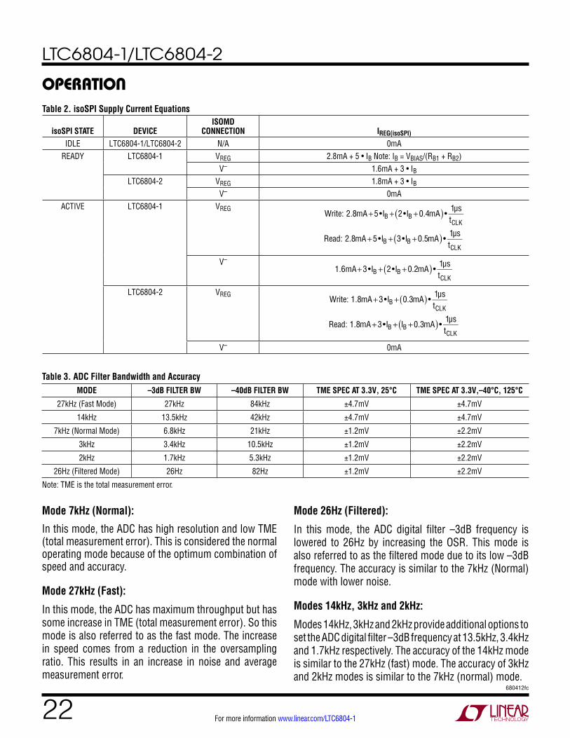
Table 2. isoSPI Supply Current Equations
isoSPI STATE DEVICEISOMD
CONNECTION IREG(isoSPI)
IDLE LTC6804-1/LTC6804-2 N/A 0mAREADY LTC6804-1 VREG 2.8mA + 5 • IB Note: IB = VBIAS/(RB1 + RB2)
V– 1.6mA + 3 • IBLTC6804-2 VREG 1.8mA + 3 • IB
V– 0mAACTIVE LTC6804-1 VREG
Write: 2.8mA +5 •IB + 2 •IB +0.4mA( ) •1µstCLK
Read: 2.8mA +5 •IB + 3 •IB +0.5mA( ) •1µstCLK
V–
1.6mA+3 •IB + 2 •IB +0.2mA( ) •
1µstCLK
LTC6804-2 VREG
Write: 1.8mA +3 •IB + 0.3mA( ) •1µstCLK
Read: 1.8mA +3 •IB + IB +0.3mA( ) •1µstCLK
V– 0mA
operaTion
Mode 7kHz (Normal):
In this mode, the ADC has high resolution and low TME (total measurement error). This is considered the normal operating mode because of the optimum combination of speed and accuracy.
Mode 27kHz (Fast):
In this mode, the ADC has maximum throughput but has some increase in TME (total measurement error). So this mode is also referred to as the fast mode. The increase in speed comes from a reduction in the oversampling ratio. This results in an increase in noise and average measurement error.
Mode 26Hz (Filtered):
In this mode, the ADC digital filter –3dB frequency is lowered to 26Hz by increasing the OSR. This mode is also referred to as the filtered mode due to its low –3dB frequency. The accuracy is similar to the 7kHz (Normal) mode with lower noise.
Modes 14kHz, 3kHz and 2kHz:
Modes 14kHz, 3kHz and 2kHz provide additional options to set the ADC digital filter –3dB frequency at 13.5kHz, 3.4kHz and 1.7kHz respectively. The accuracy of the 14kHz mode is similar to the 27kHz (fast) mode. The accuracy of 3kHz and 2kHz modes is similar to the 7kHz (normal) mode.
Table 3. ADC Filter Bandwidth and AccuracyMODE –3dB FILTER BW –40dB FILTER BW TME SPEC AT 3.3V, 25°C TME SPEC AT 3.3V,–40°C, 125°C
27kHz (Fast Mode) 27kHz 84kHz ±4.7mV ±4.7mV
14kHz 13.5kHz 42kHz ±4.7mV ±4.7mV
7kHz (Normal Mode) 6.8kHz 21kHz ±1.2mV ±2.2mV
3kHz 3.4kHz 10.5kHz ±1.2mV ±2.2mV
2kHz 1.7kHz 5.3kHz ±1.2mV ±2.2mV
26Hz (Filtered Mode) 26Hz 82Hz ±1.2mV ±2.2mV
Note: TME is the total measurement error.
LTC6804-1/LTC6804-2
23680412fc
For more information www.linear.com/LTC6804-1
operaTionThe conversion times for these modes are provided in Table 5. If the core is in STANDBY state, an additional tREFUP time is required to power up the reference before beginning the ADC conversions. The reference can remain powered up between ADC conversions if the REFON bit in Configuration Register Group is set to 1 so the core is in REFUP state after a delay tREFUP. Then, the subsequent ADC commands will not have the tREFUP delay before beginning ADC conversions.
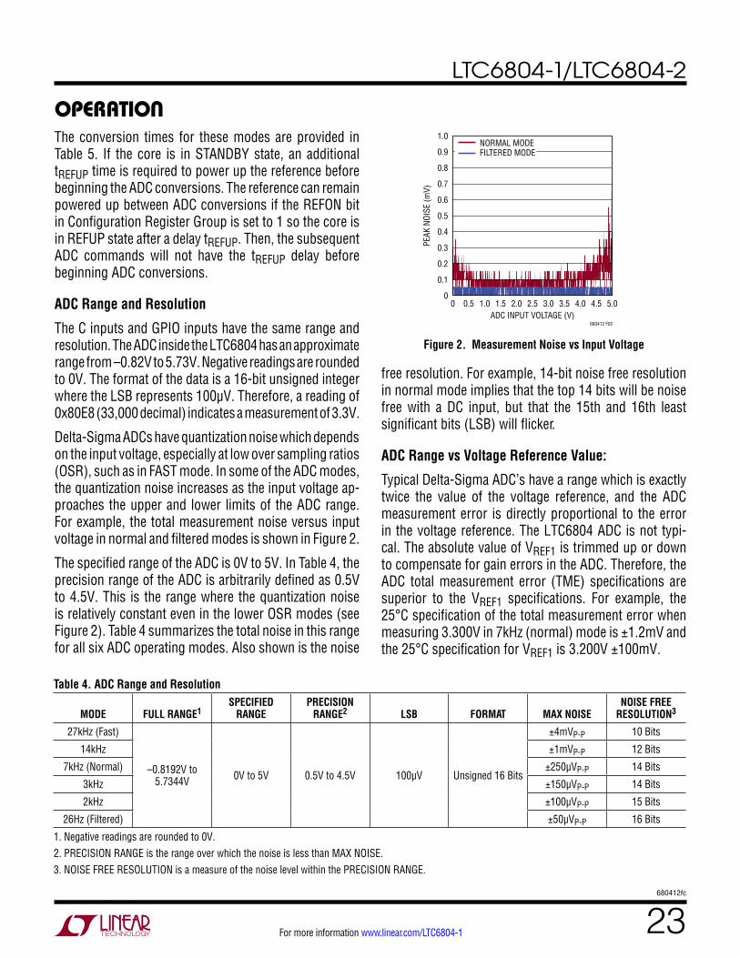
ADC Range and Resolution
The C inputs and GPIO inputs have the same range and resolution. The ADC inside the LTC6804 has an approximate range from –0.82V to 5.73V. Negative readings are rounded to 0V. The format of the data is a 16-bit unsigned integer where the LSB represents 100µV. Therefore, a reading of 0x80E8 (33,000 decimal) indicates a measurement of 3.3V.
Delta-Sigma ADCs have quantization noise which depends on the input voltage, especially at low over sampling ratios (OSR), such as in FAST mode. In some of the ADC modes, the quantization noise increases as the input voltage ap-proaches the upper and lower limits of the ADC range. For example, the total measurement noise versus input voltage in normal and filtered modes is shown in Figure 2.
The specified range of the ADC is 0V to 5V. In Table 4, the precision range of the ADC is arbitrarily defined as 0.5V to 4.5V. This is the range where the quantization noise is relatively constant even in the lower OSR modes (see Figure 2). Table 4 summarizes the total noise in this range for all six ADC operating modes. Also shown is the noise
free resolution. For example, 14-bit noise free resolution in normal mode implies that the top 14 bits will be noise free with a DC input, but that the 15th and 16th least significant bits (LSB) will flicker.
ADC Range vs Voltage Reference Value:
Typical Delta-Sigma ADC’s have a range which is exactly twice the value of the voltage reference, and the ADC measurement error is directly proportional to the error in the voltage reference. The LTC6804 ADC is not typi-cal. The absolute value of VREF1 is trimmed up or down to compensate for gain errors in the ADC. Therefore, the ADC total measurement error (TME) specifications are superior to the VREF1 specifications. For example, the 25°C specification of the total measurement error when measuring 3.300V in 7kHz (normal) mode is ±1.2mV and the 25°C specification for VREF1 is 3.200V ±100mV.
Table 4. ADC Range and Resolution
MODE FULL RANGE1SPECIFIED
RANGEPRECISION
RANGE2 LSB FORMAT MAX NOISENOISE FREE
RESOLUTION3
27kHz (Fast)
–0.8192V to 5.7344V 0V to 5V 0.5V to 4.5V 100µV Unsigned 16 Bits
±4mVP-P 10 Bits
14kHz ±1mVP-P 12 Bits
7kHz (Normal) ±250µVP-P 14 Bits
3kHz ±150µVP-P 14 Bits
2kHz ±100µVP-P 15 Bits
26Hz (Filtered) ±50µVP-P 16 Bits
1. Negative readings are rounded to 0V.2. PRECISION RANGE is the range over which the noise is less than MAX NOISE.3. NOISE FREE RESOLUTION is a measure of the noise level within the PRECISION RANGE.
Figure 2. Measurement Noise vs Input Voltage
ADC INPUT VOLTAGE (V)0 0.5
PEAK
NOI
SE (m
V)
1.0
0.1
0.2
0.3
0.4
0.5
0.6
0.7
0.8
0.9
04.03.53.02.52.01.0 1.5 4.5
680412 F02
5.0
NORMAL MODEFILTERED MODE
LTC6804-1/LTC6804-2
24680412fc
For more information www.linear.com/LTC6804-1
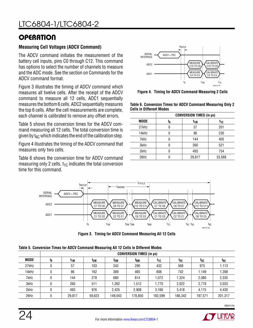
Measuring Cell Voltages (ADCV Command)
The ADCV command initiates the measurement of the battery cell inputs, pins C0 through C12. This command has options to select the number of channels to measure and the ADC mode. See the section on Commands for the ADCV command format.
Figure 3 illustrates the timing of ADCV command which measures all twelve cells. After the receipt of the ADCV command to measure all 12 cells, ADC1 sequentially measures the bottom 6 cells. ADC2 sequentially measures the top 6 cells. After the cell measurements are complete, each channel is calibrated to remove any offset errors.
Table 5 shows the conversion times for the ADCV com-mand measuring all 12 cells. The total conversion time is given by t6C which indicates the end of the calibration step.
Figure 4 illustrates the timing of the ADCV command that measures only two cells.
Table 6 shows the conversion time for ADCV command measuring only 2 cells. t1C indicates the total conversion time for this command.
operaTion
Figure 3. Timing for ADCV Command Measuring All 12 Cells
Table 6. Conversion Times for ADCV Command Measuring Only 2 Cells in Different Modes
CONVERSION TIMES (in µs)
MODE t0 t1M t1C
27kHz 0 57 201
14kHz 0 86 230
7kHz 0 144 405
3kHz 0 260 521
2kHz 0 493 754
26Hz 0 29,817 33,568
Table 5. Conversion Times for ADCV Command Measuring All 12 Cells in Different ModesCONVERSION TIMES (in µs)
MODE t0 t1M t2M t5M t6M t1C t2C t5C t6C
27kHz 0 57 103 243 290 432 568 975 1,113
14kHz 0 86 162 389 465 606 742 1,149 1,288
7kHz 0 144 278 680 814 1,072 1,324 2,080 2,335
3kHz 0 260 511 1,262 1,512 1,770 2,022 2,778 3,033
2kHz 0 493 976 2,425 2,908 3,166 3,418 4,175 4,430
26Hz 0 29,817 59,623 149,043 178,850 182,599 186,342 197,571 201,317
CALIBRATEC8 TO C7
CALIBRATEC7 TO C6
MEASUREC12 TO C11
MEASUREC8 TO C7
MEASUREC7 TO C6ADC2
SERIALINTERFACE
tCYCLEtSKEW2
ADCV + PEC
CALIBRATEC2 TO C1
CALIBRATEC12 TO C11
CALIBRATEC6 TO C5
CALIBRATEC1 TO C0
MEASUREC6 TO C5
MEASUREC2 TO C1
MEASUREC1 TO C0ADC1
t0 t1M t2M t6Mt5M t1C t2C t5C t6C680412 F03
tREFUP
Figure 4. Timing for ADCV Command Measuring 2 Cells
CALIBRATEC10 TO C9
MEASUREC10 TO C9ADC2
SERIALINTERFACE
ADCV + PEC
CALIBRATEC4 TO C3
MEASUREC4 TO C3ADC1
t0 t1M t1C680412 F04
tREFUP
LTC6804-1/LTC6804-2
25680412fc
For more information www.linear.com/LTC6804-1
operaTion
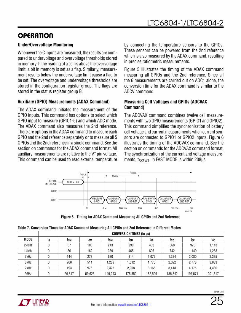
Table 7. Conversion Times for ADAX Command Measuring All GPIOs and 2nd Reference in Different ModesCONVERSION TIMES (in µs)
MODE t0 t1M t2M t5M t6M t1C t2C t5C t6C
27kHz 0 57 103 243 290 432 568 975 1,113
14kHz 0 86 162 389 465 606 742 1,149 1,288
7kHz 0 144 278 680 814 1,072 1,324 2,080 2,335
3kHz 0 260 511 1,262 1,512 1,770 2,022 2,778 3,033
2kHz 0 493 976 2,425 2,908 3,166 3,418 4,175 4,430
26Hz 0 29,817 59,623 149,043 178,850 182,599 186,342 197,571 201,317
Figure 5. Timing for ADAX Command Measuring All GPIOs and 2nd Reference
ADC2
SERIALINTERFACE
tCYCLEtSKEW
ADAX + PEC
CALIBRATEGPIO2
CALIBRATE2ND REF
CALIBRATEGPIO1
MEASURE2ND REF
MEASUREGPIO2
MEASUREGPIO1ADC1
t0 t1M t2M t6Mt5M t1C t2C t5C t6C680412 F05
tREFUP
Under/Overvoltage Monitoring
Whenever the C inputs are measured, the results are com-pared to undervoltage and overvoltage thresholds stored in memory. If the reading of a cell is above the overvoltage limit, a bit in memory is set as a flag. Similarly, measure-ment results below the undervoltage limit cause a flag to be set. The overvoltage and undervoltage thresholds are stored in the configuration register group. The flags are stored in the status register group B.
Auxiliary (GPIO) Measurements (ADAX Command)
The ADAX command initiates the measurement of the GPIO inputs. This command has options to select which GPIO input to measure (GPIO1-5) and which ADC mode. The ADAX command also measures the 2nd reference. There are options in the ADAX command to measure each GPIO and the 2nd reference separately or to measure all 5 GPIOs and the 2nd reference in a single command. See the section on commands for the ADAX command format. All auxiliary measurements are relative to the V– pin voltage. This command can be used to read external temperature
by connecting the temperature sensors to the GPIOs. These sensors can be powered from the 2nd reference which is also measured by the ADAX command, resulting in precise ratiometric measurements.
Figure 5 illustrates the timing of the ADAX command measuring all GPIOs and the 2nd reference. Since all the 6 measurements are carried out on ADC1 alone, the conversion time for the ADAX command is similar to the ADCV command.
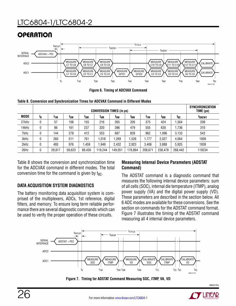
Measuring Cell Voltages and GPIOs (ADCVAX Command)
The ADCVAX command combines twelve cell measure-ments with two GPIO measurements (GPIO1 and GPIO2). This command simplifies the synchronization of battery cell voltage and current measurements when current sen-sors are connected to GPIO1 or GPIO2 inputs. Figure 6 illustrates the timing of the ADCVAX command. See the section on commands for the ADCVAX command format. The synchronization of the current and voltage measure-ments, tSKEW1, in FAST MODE is within 208µs.
LTC6804-1/LTC6804-2
26680412fc
For more information www.linear.com/LTC6804-1
operaTion
CALIBRATEMEASUREC12 TO C11
MEASUREC11 TO C10
MEASUREC10 TO C9
MEASUREC9 TO C8
MEASUREC8 TO C7
MEASUREC7 TO C6ADC2
SERIALINTERFACE
tCYCLE
tSKEW1tSKEW1
ADCVAX + PEC
CALIBRATEMEASUREC6 TO C5
MEASUREC5 TO C4
MEASUREC4 TO C3
MEASUREGPIO2
MEASUREGPIO1
MEASUREC3 TO C2
MEASUREC2 TO C1
MEASUREC1 TO C0ADC1
t0 t1M t2M t3M t4M t5M t6M t7M t8M t8C
tREFUP
680412 F06
Figure 6. Timing of ADCVAX Command
Table 8 shows the conversion and synchronization time for the ADCVAX command in different modes. The total conversion time for the command is given by t8C.
DATA ACqUISITION SYSTEM DIAGNOSTICS
The battery monitoring data acquisition system is com-prised of the multiplexers, ADCs, 1st reference, digital filters, and memory. To ensure long term reliable perfor-mance there are several diagnostic commands which can be used to verify the proper operation of these circuits.
Measuring Internal Device Parameters (ADSTAT Command)
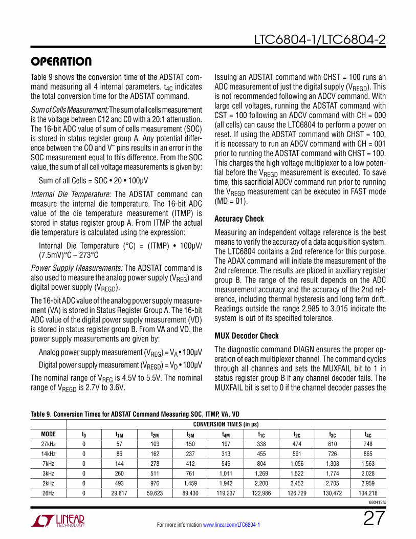
The ADSTAT command is a diagnostic command that measures the following internal device parameters: sum of all cells (SOC), internal die temperature (ITMP), analog power supply (VA) and the digital power supply (VD). These parameters are described in the section below. All 6 ADC modes are available for these conversions. See the section on commands for the ADSTAT command format. Figure 7 illustrates the timing of the ADSTAT command measuring all 4 internal device parameters.
Table 8. Conversion and Synchronization Times for ADCVAX Command in Different Modes
CONVERSION TIMES (in µs)SYNCHRONIZATION
TIME (µs)
MODE t0 t1M t2M t3M t4M t5M t6M t7M t8M t8C tSKEW1
27kHz 0 57 106 155 216 265 326 375 424 1,564 208
14kHz 0 86 161 237 320 396 479 555 630 1,736 310
7kHz 0 144 278 412 553 687 828 962 1,096 3,133 543
3kHz 0 260 511 761 1,018 1,269 1,526 1,777 2,027 4,064 1009
2kHz 0 493 976 1,459 1,949 2,432 2,923 3,406 3,888 5,925 1939
26Hz 0 29,817 59,623 89,430 119,244 149,051 178,864 208,671 238,478 268,442 119234
Figure 7. Timing for ADSTAT Command Measuring SOC, ITMP, VA, VD
ADC2
SERIALINTERFACE
tCYCLEtSKEW
ADSTAT + PEC
CALIBRATEITMP
CALIBRATEVD
CALIBRATESOC
MEASUREVD
MEASUREITMP
MEASURESOCADC1
t0 t1M t2M t4Mt3M t1C t2C t3C t4C680412 F07
tREFUP
LTC6804-1/LTC6804-2
27680412fc
For more information www.linear.com/LTC6804-1
operaTion
Table 9. Conversion Times for ADSTAT Command Measuring SOC, ITMP, VA, VDCONVERSION TIMES (in µs)
MODE t0 t1M t2M t3M t4M t1C t2C t3C t4C
27kHz 0 57 103 150 197 338 474 610 748
14kHz 0 86 162 237 313 455 591 726 865
7kHz 0 144 278 412 546 804 1,056 1,308 1,563
3kHz 0 260 511 761 1,011 1,269 1,522 1,774 2,028
2kHz 0 493 976 1,459 1,942 2,200 2,452 2,705 2,959
26Hz 0 29,817 59,623 89,430 119,237 122,986 126,729 130,472 134,218
Table 9 shows the conversion time of the ADSTAT com-mand measuring all 4 internal parameters. t4C indicates the total conversion time for the ADSTAT command.
Sum of Cells Measurement: The sum of all cells measurement is the voltage between C12 and C0 with a 20:1 attenuation. The 16-bit ADC value of sum of cells measurement (SOC) is stored in status register group A. Any potential differ-ence between the CO and V– pins results in an error in the SOC measurement equal to this difference. From the SOC value, the sum of all cell voltage measurements is given by:
Sum of all Cells = SOC • 20 • 100µV
Internal Die Temperature: The ADSTAT command can measure the internal die temperature. The 16-bit ADC value of the die temperature measurement (ITMP) is stored in status register group A. From ITMP the actual die temperature is calculated using the expression:
Internal Die Temperature (°C) = (ITMP) • 100µV/(7.5mV)°C – 273°C
Power Supply Measurements: The ADSTAT command is also used to measure the analog power supply (VREG) and digital power supply (VREGD).
The 16-bit ADC value of the analog power supply measure-ment (VA) is stored in Status Register Group A. The 16-bit ADC value of the digital power supply measurement (VD) is stored in status register group B. From VA and VD, the power supply measurements are given by:
Analog power supply measurement (VREG) = VA • 100µV
Digital power supply measurement (VREGD) = VD • 100µV
The nominal range of VREG is 4.5V to 5.5V. The nominal range of VREGD is 2.7V to 3.6V.
Issuing an ADSTAT command with CHST = 100 runs an ADC measurement of just the digital supply (VREGD). This is not recommended following an ADCV command. With large cell voltages, running the ADSTAT command with CST = 100 following an ADCV command with CH = 000 (all cells) can cause the LTC6804 to perform a power on reset. If using the ADSTAT command with CHST = 100, it is necessary to run an ADCV command with CH = 001 prior to running the ADSTAT command with CHST = 100. This charges the high voltage multiplexer to a low poten-tial before the VREGD measurement is executed. To save time, this sacrificial ADCV command run prior to running the VREGD measurement can be executed in FAST mode (MD = 01).
Accuracy Check
Measuring an independent voltage reference is the best means to verify the accuracy of a data acquisition system. The LTC6804 contains a 2nd reference for this purpose. The ADAX command will initiate the measurement of the 2nd reference. The results are placed in auxiliary register group B. The range of the result depends on the ADC measurement accuracy and the accuracy of the 2nd ref-erence, including thermal hysteresis and long term drift. Readings outside the range 2.985 to 3.015 indicate the system is out of its specified tolerance.
MUX Decoder Check
The diagnostic command DIAGN ensures the proper op-eration of each multiplexer channel. The command cycles through all channels and sets the MUXFAIL bit to 1 in status register group B if any channel decoder fails. The MUXFAIL bit is set to 0 if the channel decoder passes the
LTC6804-1/LTC6804-2
28680412fc
For more information www.linear.com/LTC6804-1
operaTiontest. The MUXFAIL bit is also set to 1 on power-up (POR) or after a CLRSTAT command.
The DIAGN command takes about 400µs to complete if the core is in REFUP state and about 4.5ms to complete if the core is in STANDBY state. The polling methods described in the section Polling Methods can be used to determine the completion of the DIAGN command.
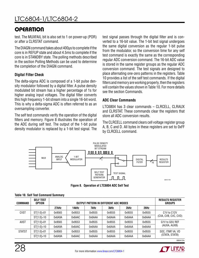
Digital Filter Check
The delta-sigma ADC is composed of a 1-bit pulse den-sity modulator followed by a digital filter. A pulse density modulated bit stream has a higher percentage of 1s for higher analog input voltages. The digital filter converts this high frequency 1-bit stream into a single 16-bit word. This is why a delta-sigma ADC is often referred to as an oversampling converter.
The self test commands verify the operation of the digital filters and memory. Figure 8 illustrates the operation of the ADC during self test. The output of the 1-bit pulse density modulator is replaced by a 1-bit test signal. The
Table 10. Self Test Command Summary
COMMANDSELF TEST
OPTION OUTPUT PATTERN IN DIFFERENT ADC MODESRESULTS REGISTER
GROUPS
27kHz 14kHz 7kHz 3kHz 2kHz 26Hz
CVST ST[1:0]=01 0x9565 0x9553 0x9555 0x9555 0x9555 0x9555 C1V to C12V (CVA, CVB, CVC, CVD)ST[1:0]=10 0x6A9A 0x6AAC 0x6AAA 0x6AAA 0x6AAA 0x6AAA
AXST ST[1:0]=01 0x9565 0x9553 0x9555 0x9555 0x9555 0x9555 G1V to G5V, REF (AUXA, AUXB)ST[1:0]=10 0x6A9A 0x6AAC 0x6AAA 0x6AAA 0x6AAA 0x6AAA
STATST ST[1:0]=01 0x9565 0x9553 0x9555 0x9555 0x9555 0x9555 SOC, ITMP, VA, VD (STATA, STATB)ST[1:0]=10 0x6A9A 0x6AAC 0x6AAA 0x6AAA 0x6AAA 0x6AAA
Figure 8. Operation of LTC6804 ADC Self Test
680412 F08
RESULTSREGISTER
DIGITALFILTER
ANALOGINPUTMUX
TEST SIGNAL
PULSE DENSITYMODULATEDBIT STREAM
1
SELF TESTPATTERN
GENERATOR
16
1-BITMODULATOR
test signal passes through the digital filter and is con-verted to a 16-bit value. The 1-bit test signal undergoes the same digital conversion as the regular 1-bit pulse from the modulator, so the conversion time for any self test command is exactly the same as the corresponding regular ADC conversion command. The 16-bit ADC value is stored in the same register groups as the regular ADC conversion command. The test signals are designed to place alternating one-zero patterns in the registers. Table 10 provides a list of the self test commands. If the digital filters and memory are working properly, then the registers will contain the values shown in Table 10. For more details see the section Commands.
ADC Clear Commands
LTC6804 has 3 clear commands – CLRCELL, CLRAUX and CLRSTAT. These commands clear the registers that store all ADC conversion results.
The CLRCELL command clears cell voltage register group A, B, C and D. All bytes in these registers are set to 0xFF by CLRCELL command.
LTC6804-1/LTC6804-2
29680412fc
For more information www.linear.com/LTC6804-1
operaTionThe CLRAUX command clears auxiliary register group A and B. All bytes in these registers are set to 0xFF by CLRAUX command.
The CLRSTAT command clears status register group A and B except the REVCODE and RSVD bits in status register group B. A read back of REVCODE will return the revision code of the part. All OV flags, UV flags, MUXFAIL bit, and THSD bit in status register group B are set to 1 by CLR-STAT command. The THSD bit is set to 0 after RDSTATB command. The registers storing SOC, ITMP, VA and VD are all set to 0xFF by CLRSTAT command.
Open-Wire Check (ADOW Command)
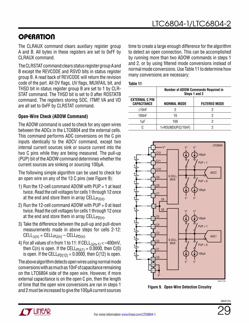
The ADOW command is used to check for any open wires between the ADCs in the LTC6804 and the external cells. This command performs ADC conversions on the C pin inputs identically to the ADCV command, except two internal current sources sink or source current into the two C pins while they are being measured. The pull-up (PUP) bit of the ADOW command determines whether the current sources are sinking or sourcing 100µA.
The following simple algorithm can be used to check for an open wire on any of the 13 C pins (see Figure 9):
1) Run the 12-cell command ADOW with PUP = 1 at least twice. Read the cell voltages for cells 1 through 12 once at the end and store them in array CELLPU(n).
2) Run the 12-cell command ADOW with PUP = 0 at least twice. Read the cell voltages for cells 1 through 12 once at the end and store them in array CELLPD(n).
3) Take the difference between the pull-up and pull-down measurements made in above steps for cells 2-12: CELL∆(n) = CELLPU(n) – CELLPD(n).
4) For all values of n from 1 to 11: If CELL∆(n+1) < –400mV, then C(n) is open. If the CELLPU(1) = 0.0000, then C(0) is open. If the CELLPD(12) = 0.0000, then C(12) is open.
The above algorithm detects open wires using normal mode conversions with as much as 10nF of capacitance remaining on the LTC6804 side of the open wire. However, if more external capacitance is on the open C pin, then the length of time that the open wire conversions are ran in steps 1 and 2 must be increased to give the 100µA current sources
time to create a large enough difference for the algorithm to detect an open connection. This can be accomplished by running more than two ADOW commands in steps 1 and 2, or by using filtered mode conversions instead of normal mode conversions. Use Table 11 to determine how many conversions are necessary:
Table 11Number of ADOW Commands Required in
Steps 1 and 2
EXTERNAL C PIN CAPACITANCE NORMAL MODE FILTERED MODE
≤10nF 2 2
100nF 10 2
1µF 100 2
C 1+ROUNDUP(C/10nF) 2
2+
+
+
+
+
+
+
V+
V–
100µA
100µA
PUP = 1
C12
PUP = 0
V+V+
V–
ADC2
LTC6804
4C11
6C10
8C9 6-CELL
MUX
10C8
12
14
C7
C6
C6
1
16+
+
+
+
+
V+
V–
100µA
100µA
PUP = 1
C5
PUP = 0
V+
V–
V–
680412 F09
ADC1
18C4
20C3
22C2 6-CELL
MUX
24C1
26
30
31
C0
Figure 9. Open-Wire Detection Circuitry
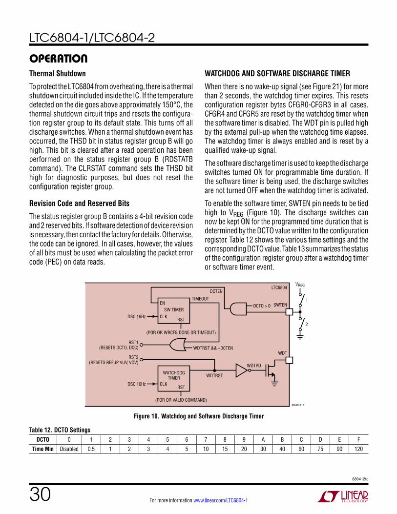
LTC6804-1/LTC6804-2
30680412fc
For more information www.linear.com/LTC6804-1
operaTionThermal Shutdown
To protect the LTC6804 from overheating, there is a thermal shutdown circuit included inside the IC. If the temperature detected on the die goes above approximately 150°C, the thermal shutdown circuit trips and resets the configura-tion register group to its default state. This turns off all discharge switches. When a thermal shutdown event has occurred, the THSD bit in status register group B will go high. This bit is cleared after a read operation has been performed on the status register group B (RDSTATB command). The CLRSTAT command sets the THSD bit high for diagnostic purposes, but does not reset the configuration register group.
Revision Code and Reserved Bits
The status register group B contains a 4-bit revision code and 2 reserved bits. If software detection of device revision is necessary, then contact the factory for details. Otherwise, the code can be ignored. In all cases, however, the values of all bits must be used when calculating the packet error code (PEC) on data reads.
WATCHDOG AND SOFTWARE DISCHARGE TIMER
When there is no wake-up signal (see Figure 21) for more than 2 seconds, the watchdog timer expires. This resets configuration register bytes CFGR0-CFGR3 in all cases. CFGR4 and CFGR5 are reset by the watchdog timer when the software timer is disabled. The WDT pin is pulled high by the external pull-up when the watchdog time elapses. The watchdog timer is always enabled and is reset by a qualified wake-up signal.
The software discharge timer is used to keep the discharge switches turned ON for programmable time duration. If the software timer is being used, the discharge switches are not turned OFF when the watchdog timer is activated.
To enable the software timer, SWTEN pin needs to be tied high to VREG (Figure 10). The discharge switches can now be kept ON for the programmed time duration that is determined by the DCTO value written to the configuration register. Table 12 shows the various time settings and the corresponding DCTO value. Table 13 summarizes the status of the configuration register group after a watchdog timer or software timer event.
Table 12. DCTO SettingsDCTO 0 1 2 3 4 5 6 7 8 9 A B C D E F
Time Min Disabled 0.5 1 2 3 4 5 10 15 20 30 40 60 75 90 120
Figure 10. Watchdog and Software Discharge Timer
680412 F10
VREG
SWTEN
LTC6804
DCTO > 0
2
SW TIMER
TIMEOUT
DCTEN
EN
RSTCLK
1
RST
(POR OR WRCFG DONE OR TIMEOUT)
(POR OR VALID COMMAND)
CLK
OSC 16Hz
OSC 16Hz
WDT
WDTPD
WDTRST && ~DCTENRST1
(RESETS DCTO, DCC)
RST2(RESETS REFUP, VUV, VOV)
WDTRSTWATCHDOGTIMER
LTC6804-1/LTC6804-2
31680412fc
For more information www.linear.com/LTC6804-1
operaTion
Table 15. COMM Register Memory MapREGISTER RD/WR BIT 7 BIT 6 BIT 5 BIT 4 BIT 3 BIT 2 BIT 1 BIT 0COMM0 RD/WR ICOM0[3] ICOM0[2] ICOM0[1] ICOM0[0] D0[7] D0[6] D0[5] D0[4]
COMM1 RD/WR D0[3] D0[2] D0[1] D0[0] FCOM0[3] FCOM0[2] FCOM0[1] FCOM0[0]
COMM2 RD/WR ICOM1[3] ICOM1[2] ICOM1[1] ICOM1[0] D1[7] D1[6] D1[5] D1[4]
COMM3 RD/WR D1[3] D1[2] D1[1] D1[0] FCOM1[3] FCOM1[2] FCOM1[1] FCOM1[0]
COMM4 RD/WR ICOM2[3] ICOM2[2] ICOM2[1] ICOM2[0] D2[7] D2[6] D2[5] D2[4]
COMM5 RD/WR D2[3] D2[2] D2[1] D2[0] FCOM2[3] FCOM2[2] FCOM2[1] FCOM2[0]
Table 13WATCHDOG TIMER SOFTWARE TIMER
SWTEN = 0, DCTO = XXXX Resets CFGR0-5 When It Activates
Disabled
SWTEN = 1, DCTO = 0000 Resets CFGR0-5 When It Activates
Disabled
SWTEN = 1, DCTO ! = 0000 Resets CFGR0-3 When It Activates
Resets CFGR4-5 When It Fires
Unlike the watchdog timer, the software timer does not reset when there is a valid command. The software timer can only be reset after a valid WRCFG (write configuration register) command. There is a possibility that the software timer will expire in the middle of some commands.
If software timer activates in the middle of WRCFG com-mand, the configuration register resets as per Table 14. However, at the end of the valid WRCFG command, the new data is copied to the configuration register. The new data is not lost when the software timer is activated.
If software timer activates in the middle of RDCFG com-mand, the configuration register group resets as per Table 14. As a result, the read back data from bytes CRFG4 and CRFG5 could be corrupted.
I2C/SPI MASTER ON LTC6804 USING GPIOS
The I/O ports GPIO3, GPIO4 and GPIO5 on LTC6804-1 and LTC6804-2 can be used as an I2C or SPI master port to communicate to an I2C or SPI slave. In the case of an I2C master, GPIO4 and GPIO5 form the SDA and SCL ports of the I2C interface respectively. In the case of a SPI master, GPIO3, GPIO5 and GPIO4 become the chip select (CSBM), clock (SCKM) and data (SDIOM) ports of the SPI interface respectively. The SPI master on LTC6804 supports only SPI mode 3 (CHPA = 1, CPOL = 1).
Table 14DCTO
(READ VALUE) TIME LEFT (MIN)
0 Disabled (or) Timer Has Timed Out
1 0 < Timer ≤ 0.5
2 0.5 < Timer ≤ 1
3 1 < Timer ≤ 2
4 2 < Timer ≤ 3
5 3 < Timer ≤ 4
6 4 < Timer ≤ 5
7 5 < Timer ≤ 10
8 10 < Timer ≤ 15
9 15 < Timer ≤ 20
A 20 < Timer ≤ 30
B 30 < Timer ≤ 40
C 40 < Timer ≤ 60
D 60 < Timer ≤ 75
E 75 < Timer ≤ 90
F 90 < Timer ≤ 120
The GPIOs are open drain outputs, so an external pull-up is required on these ports to operate as an I2C or SPI master. It is also important to write the GPIO bits to 1 in the CFG register group so these ports are not pulled low internally by the device.
COMM Register
LTC6804 has a 6-byte COMM register as shown in Table 15. This register stores all data and control bits required for I2C or SPI communication to a slave. The COMM register contains 3 bytes of data Dn[7:0] to be transmitted to or received from the slave device. ICOMn [3:0] specify con-trol actions before transmitting/receiving the data byte. FCOMn [3:0] specify control actions after transmitting/ receiving the data byte.
LTC6804-1/LTC6804-2
32680412fc
For more information www.linear.com/LTC6804-1
operaTion
Table 17. Write Codes for ICOMn[3:0] and FCOMn[3:0] on SPI MasterCONTROL BITS CODE ACTION DESCRIPTION
ICOMn[3:0]
1000 CSBM low Generates a CSBM Low Signal on SPI Port (GPIO3)
1001 CSBM high Generates a CSBM High Signal on SPI Port (GPIO3)
1111 No Transmit Releases the SPI Port and Ignores the Rest of the Data
FCOMn[3:0]X000 CSBM low Holds CSBM Low at the End of Byte Transmission
1001 CSBM high Transitions CSBM High at the End of Byte Transmission
Table 16. Write Codes for ICOMn[3:0] and FCOMn[3:0] on I2C MasterCONTROL BITS CODE ACTION DESCRIPTION
ICOMn[3:0]
0110 START Generate a START Signal on I2C Port Followed By Data Transmission
0001 STOP Generate a STOP Signal on I2C port
0000 BLANK Proceed Directly to Data Transmission on I2C Port
0111 No Transmit Release SDA and SCL and Ignore the Rest of the Data
FCOMn[3:0]
0000 Master ACK Master Generates an ACK Signal on Ninth Clock Cycle
1000 Master NACK Master Generates a NACK Signal on Ninth Clock Cycle
1001 Master NACK + STOP Master Generates a NACK Signal Followed by STOP Signal
If the bit ICOMn[3] in the COMM register is set to 1 the part becomes an I2C master and if the bit is set to 0 the part becomes a SPI master.
Table 16 describes the valid write codes for ICOMn[3:0] and FCOMn[3:0] and their behavior when using the part as an I2C master.
Table 17 describes the valid codes for ICOMn[3:0] and FCOMn[3:0] and their behavior when using the part as a SPI master.
Note that only the codes listed in Tables 16 and 17 are valid for ICOMn[3:0] and FCOMn[3:0]. Writing any other code that is not listed in Tables 16 and 17 to ICOMn[3:0] and FCOMn[3:0] may result in unexpected behavior on the I2C and SPI ports.
COMM Commands
Three commands help accomplish I2C or SPI communica-tion to the slave device: WRCOMM, STCOMM, RDCOMM
WRCOMM Command: This command is used to write data to the COMM register. This command writes 6 bytes of data to the COMM register. The PEC needs to be written
at the end of the data. If the PEC does not match, all data in the COMM register is cleared to 1’s when CSB goes high. See the section Bus Protocols for more details on a write command format.
STCOMM Command: This command initiates I2C/SPI com-munication on the GPIO ports. The COMM register contains 3 bytes of data to be transmitted to the slave. During this command, the data bytes stored in the COMM register are transmitted to the slave I2C or SPI device and the data received from the I2C or SPI device is stored in the COMM register. This command uses GPIO4 (SDA) and GPIO5 (SCL) for I2C communication or GPIO3 (CSBM), GPIO4 (SDIOM) and GPIO5 (SCKM) for SPI communication.
The STCOMM command is to be followed by 24 clock cycles for each byte of data to be transmitted to the slave device while holding CSB low. For example, to transmit 3 bytes of data to the slave, send STCOMM command and its PEC followed by 72 clock cycles. Pull CSB high at the end of the 72 clock cycles of STCOMM command.
During I2C or SPI communication, the data received from the slave device is updated in the COMM register.
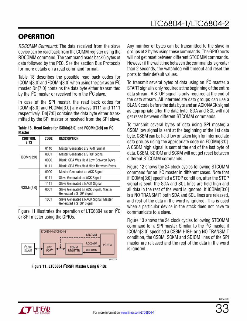
LTC6804-1/LTC6804-2
33680412fc
For more information www.linear.com/LTC6804-1
Figure 11. LTC6804 I2C/SPI Master Using GPIOs
680412 F11
COMMREGISTER
GPIOPORT
I2C/SPISLAVE
PORT ARDCOMM
WRCOMM
STCOMMLTC6804-1/LTC6804-2
operaTionAny number of bytes can be transmitted to the slave in groups of 3 bytes using these commands. The GPIO ports will not get reset between different STCOMM commands. However, if the wait time between the commands is greater than 2 seconds, the watchdog will timeout and reset the ports to their default values.
To transmit several bytes of data using an I2C master, a START signal is only required at the beginning of the entire data stream. A STOP signal is only required at the end of the data stream. All intermediate data groups can use a BLANK code before the data byte and an ACK/NACK signal as appropriate after the data byte. SDA and SCL will not get reset between different STCOMM commands.
To transmit several bytes of data using SPI master, a CSBM low signal is sent at the beginning of the 1st data byte. CSBM can be held low or taken high for intermediate data groups using the appropriate code on FCOMn[3:0]. A CSBM high signal is sent at the end of the last byte of data. CSBM, SDIOM and SCKM will not get reset between different STCOMM commands.
Figure 12 shows the 24 clock cycles following STCOMM command for an I2C master in different cases. Note that if ICOMn[3:0] specified a STOP condition, after the STOP signal is sent, the SDA and SCL lines are held high and all data in the rest of the word is ignored. If ICOMn[3:0] is a NO TRANSMIT, both SDA and SCL lines are released, and rest of the data in the word is ignored. This is used when a particular device in the stack does not have to communicate to a slave.
Figure 13 shows the 24 clock cycles following STCOMM command for a SPI master. Similar to the I2C master, if ICOMn[3:0] specified a CSBM HIGH or a NO TRANSMIT condition, the CSBM, SCKM and SDIOM lines of the SPI master are released and the rest of the data in the word is ignored.
RDCOMM Command: The data received from the slave device can be read back from the COMM register using the RDCOMM command. The command reads back 6 bytes of data followed by the PEC. See the section Bus Protocols for more details on a read command format.
Table 18 describes the possible read back codes for ICOMn[3:0] and FCOMn[3:0] when using the part as an I2C master. Dn[7:0] contains the data byte either transmitted by the I2C master or received from the I2C slave.
In case of the SPI master, the read back codes for ICOMn[3:0] and FCOMn[3:0] are always 0111 and 1111 respectively. Dn[7:0] contains the data byte either trans-mitted by the SPI master or received from the SPI slave.
Table 18. Read Codes for ICOMn[3:0] and FCOMn[3:0] on I2C Master
CONTROL BITS
CODE DESCRIPTION
ICOMn[3:0]
0110 Master Generated a START Signal
0001 Master Generated a STOP Signal
0000 Blank, SDA Was Held Low Between Bytes
0111 Blank, SDA Was Held High Between Bytes
FCOMn[3:0]
0000 Master Generated an ACK Signal
0111 Slave Generated an ACK Signal
1111 Slave Generated a NACK Signal
0001 Slave Generated an ACK Signal, Master Generated a STOP Signal
1001 Slave Generated a NACK Signal, Master Generated a STOP Signal
Figure 11 illustrates the operation of LTC6804 as an I2C or SPI master using the GPIOs.
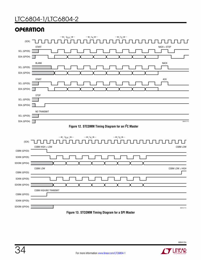
LTC6804-1/LTC6804-2
34680412fc
For more information www.linear.com/LTC6804-1
operaTion
Figure 13. STCOMM Timing Diagram for a SPI Master
SDIOM (GPIO4)680412 F13
SCKM (GPIO5)
CSBM HIGH/NO TRANSMIT
CSBM (GPIO3)
SDIOM (GPIO4)
SCKM (GPIO5)
CSBM (GPIO3)
CSBM LOW CSBM LOW ≥ HIGH
SDIOM (GPIO4)
SCKM (GPIO5)
CSBM (GPIO3)
CSBM HIGH ≥ LOW CSBM LOW
(SCK)
tCLK t4 t3
Figure 12. STCOMM Timing Diagram for an I2C Master
SDA (GPIO4) 680412 F12
SCL (GPIO5)
NO TRANSMIT
SDA (GPIO4)
SCL (GPIO5)
STOP
SDA (GPIO4)
SCL (GPIO5)
START ACK
SDA (GPIO4)
SCL (GPIO5)
START NACK + STOP
SDA (GPIO4)
SCL (GPIO5)
BLANK NACK
(SCK)
tCLK t4 t3
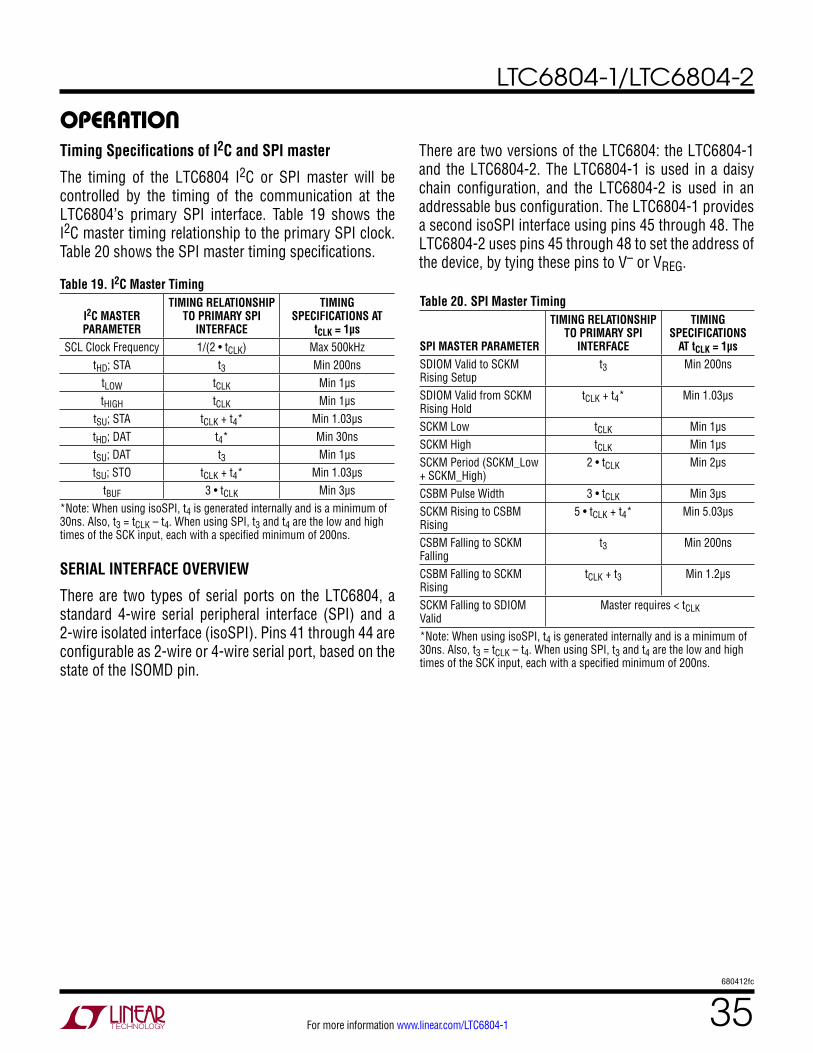
LTC6804-1/LTC6804-2
35680412fc
For more information www.linear.com/LTC6804-1
operaTion
Table 19. I2C Master Timing
I2C MASTER PARAMETER
TIMING RELATIONSHIP TO PRIMARY SPI
INTERFACE
TIMING SPECIFICATIONS AT
tCLK = 1µsSCL Clock Frequency 1/(2 • tCLK) Max 500kHz
tHD; STA t3 Min 200nstLOW tCLK Min 1µs tHIGH tCLK Min 1µs
tSU; STA tCLK + t4* Min 1.03µstHD; DAT t4* Min 30nstSU; DAT t3 Min 1µstSU; STO tCLK + t4* Min 1.03µs
tBUF 3 • tCLK Min 3µs*Note: When using isoSPI, t4 is generated internally and is a minimum of 30ns. Also, t3 = tCLK – t4. When using SPI, t3 and t4 are the low and high times of the SCK input, each with a specified minimum of 200ns.
Table 20. SPI Master Timing
SPI MASTER PARAMETER
TIMING RELATIONSHIP TO PRIMARY SPI
INTERFACE
TIMING SPECIFICATIONS
AT tCLK = 1µsSDIOM Valid to SCKM Rising Setup
t3 Min 200ns
SDIOM Valid from SCKM Rising Hold
tCLK + t4* Min 1.03µs
SCKM Low tCLK Min 1µsSCKM High tCLK Min 1µsSCKM Period (SCKM_Low + SCKM_High)
2 • tCLK Min 2µs
CSBM Pulse Width 3 • tCLK Min 3µsSCKM Rising to CSBM Rising
5 • tCLK + t4* Min 5.03µs
CSBM Falling to SCKM Falling
t3 Min 200ns
CSBM Falling to SCKM Rising
tCLK + t3 Min 1.2µs
SCKM Falling to SDIOM Valid
Master requires < tCLK
*Note: When using isoSPI, t4 is generated internally and is a minimum of 30ns. Also, t3 = tCLK – t4. When using SPI, t3 and t4 are the low and high times of the SCK input, each with a specified minimum of 200ns.
Timing Specifications of I2C and SPI master
The timing of the LTC6804 I2C or SPI master will be controlled by the timing of the communication at the LTC6804’s primary SPI interface. Table 19 shows the I2C master timing relationship to the primary SPI clock. Table 20 shows the SPI master timing specifications.
There are two versions of the LTC6804: the LTC6804-1 and the LTC6804-2. The LTC6804-1 is used in a daisy chain configuration, and the LTC6804-2 is used in an addressable bus configuration. The LTC6804-1 provides a second isoSPI interface using pins 45 through 48. The LTC6804-2 uses pins 45 through 48 to set the address of the device, by tying these pins to V– or VREG.
SERIAL INTERFACE OVERVIEW
There are two types of serial ports on the LTC6804, a standard 4-wire serial peripheral interface (SPI) and a 2-wire isolated interface (isoSPI). Pins 41 through 44 are configurable as 2-wire or 4-wire serial port, based on the state of the ISOMD pin.
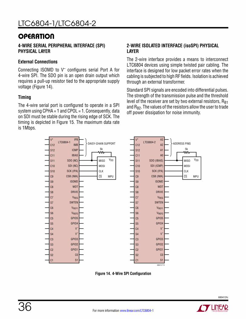
LTC6804-1/LTC6804-2
36680412fc
For more information www.linear.com/LTC6804-1
Figure 14. 4-Wire SPI Configuration
DAISY-CHAIN SUPPORT
680412 F14
V+
C12
S12
C11
S11
C10
S10
C9
S9
C8
S8
C7
S7
C6
S6
C5
S5
C4
S4
C3
S3
C2
S2
C1
MISO
MOSI
CLK
CS
VDD
MPU
IPB
IMB
ICMP
IBIAS
SDO (NC)
SDI (NC)
SCK (IPA)
CSB (IMA)
ISOMD
WDT
DRIVE
VREG
SWTEN
VREF1
VREF2
GPIO5
GPIO4
V–
V–
GPIO3
GPIO2
GPIO1
C0
S1
LTC6804-1 ADDRESS PINS
5k 5k
V+
C12
S12
C11
S11
C10
S10
C9
S9
C8
S8
C7
S7
C6
S6
C5
S5
C4
S4
C3
S3
C2
S2
C1
MISO
MOSI
CLK
CS
VDD
MPU
A3
A2
A1
A0
SDO (IBIAS)
SDI (ICMP)
SCK (IPA)
CSB (IMA)
ISOMD
WDT
DRIVE
VREG
SWTEN
VREF1
VREF2
GPIO5
GPIO4
V–
V–
GPIO3
GPIO2
GPIO1
C0
S1
LTC6804-2
operaTion4-WIRE SERIAL PERIPHERAL INTERFACE (SPI) PHYSICAL LAYER
External Connections
Connecting ISOMD to V– configures serial Port A for 4-wire SPI. The SDO pin is an open drain output which requires a pull-up resistor tied to the appropriate supply voltage (Figure 14).
Timing
The 4-wire serial port is configured to operate in a SPI system using CPHA = 1 and CPOL = 1. Consequently, data on SDI must be stable during the rising edge of SCK. The timing is depicted in Figure 15. The maximum data rate is 1Mbps.
2-WIRE ISOLATED INTERFACE (isoSPI) PHYSICAL LAYER
The 2-wire interface provides a means to interconnect LTC6804 devices using simple twisted pair cabling. The interface is designed for low packet error rates when the cabling is subjected to high RF fields. Isolation is achieved through an external transformer.
Standard SPI signals are encoded into differential pulses. The strength of the transmission pulse and the threshold level of the receiver are set by two external resistors, RB1 and RB2. The values of the resistors allow the user to trade off power dissipation for noise immunity.
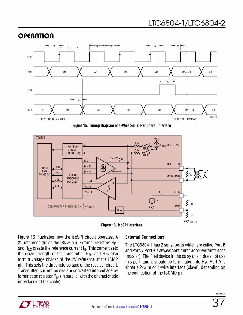
LTC6804-1/LTC6804-2
37680412fc
For more information www.linear.com/LTC6804-1
operaTion
Figure 15. Timing Diagram of 4-Wire Serial Peripheral Interface
Figure 16. isoSPI Interface
Figure 16 illustrates how the isoSPI circuit operates. A 2V reference drives the IBIAS pin. External resistors RB1 and RB2 create the reference current IB. This current sets the drive strength of the transmitter. RB1 and RB2 also form a voltage divider of the 2V reference at the ICMP pin. This sets the threshold voltage of the receiver circuit. Transmitted current pulses are converted into voltage by termination resistor RM (in parallel with the characteristic impedance of the cable).
External Connections
The LTC6804-1 has 2 serial ports which are called Port B and Port A. Port B is always configured as a 2-wire interface (master). The final device in the daisy chain does not use this port, and it should be terminated into RM. Port A is either a 2-wire or 4-wire interface (slave), depending on the connection of the ISOMD pin.
680412 F15
SDI
SCK
D3 D2 D1 D0 D7…D4 D3
CURRENT COMMANDPREVIOUS COMMAND
t7
t8
t6
t5
SDO
CSB
D3D4 D2 D1 D0 D7…D4 D3
t1 t2t3t4
680412 F16
IMA OR IMBRM
IBIAS
VICMP/3 + 167mV
IB
RB1ICMP
2V
IPA OR IPBLOGICAND
MEMORY
Tx = +1Tx • 20 • IB
Tx = –1
SDO Tx = 0
PULSEENCODER/DECODER
SDI
SCK
CSB
WAKEUPCIRCUIT
(ON PORT A)
LTC6804
+–
+–
–
+•
•
Rx = +1
Rx = –1
Rx = 0
35k
IDLE
VREG
IDLE
35k
RB2
COMPARATOR THRESHOLD = • VICMP21
0.5x
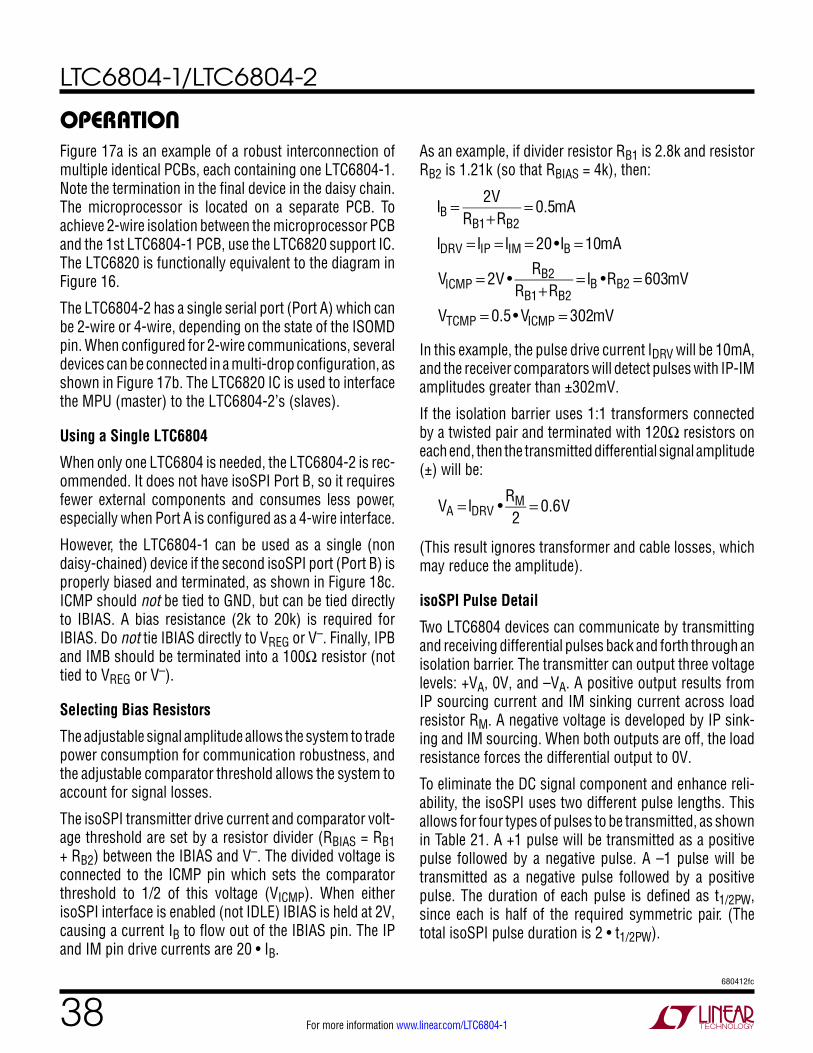
LTC6804-1/LTC6804-2
38680412fc
For more information www.linear.com/LTC6804-1
operaTionFigure 17a is an example of a robust interconnection of multiple identical PCBs, each containing one LTC6804-1. Note the termination in the final device in the daisy chain. The microprocessor is located on a separate PCB. To achieve 2-wire isolation between the microprocessor PCB and the 1st LTC6804-1 PCB, use the LTC6820 support IC. The LTC6820 is functionally equivalent to the diagram in Figure 16.
The LTC6804-2 has a single serial port (Port A) which can be 2-wire or 4-wire, depending on the state of the ISOMD pin. When configured for 2-wire communications, several devices can be connected in a multi-drop configuration, as shown in Figure 17b. The LTC6820 IC is used to interface the MPU (master) to the LTC6804-2’s (slaves).
Using a Single LTC6804
When only one LTC6804 is needed, the LTC6804-2 is rec-ommended. It does not have isoSPI Port B, so it requires fewer external components and consumes less power, especially when Port A is configured as a 4-wire interface.
However, the LTC6804-1 can be used as a single (non daisy-chained) device if the second isoSPI port (Port B) is properly biased and terminated, as shown in Figure 18c. ICMP should not be tied to GND, but can be tied directly to IBIAS. A bias resistance (2k to 20k) is required for IBIAS. Do not tie IBIAS directly to VREG or V–. Finally, IPB and IMB should be terminated into a 100Ω resistor (not tied to VREG or V–).
Selecting Bias Resistors
The adjustable signal amplitude allows the system to trade power consumption for communication robustness, and the adjustable comparator threshold allows the system to account for signal losses.
The isoSPI transmitter drive current and comparator volt-age threshold are set by a resistor divider (RBIAS = RB1 + RB2) between the IBIAS and V–. The divided voltage is connected to the ICMP pin which sets the comparator threshold to 1/2 of this voltage (VICMP). When either isoSPI interface is enabled (not IDLE) IBIAS is held at 2V, causing a current IB to flow out of the IBIAS pin. The IP and IM pin drive currents are 20 • IB.
As an example, if divider resistor RB1 is 2.8k and resistor RB2 is 1.21k (so that RBIAS = 4k), then:
IB = 2VRB1+RB2
= 0.5mA
IDRV = IIP = IIM = 20 •IB = 10mA
VICMP = 2V •RB2
RB1+RB2= IB •RB2 = 603mV
VTCMP = 0.5 • VICMP = 302mV
In this example, the pulse drive current IDRV will be 10mA, and the receiver comparators will detect pulses with IP-IM amplitudes greater than ±302mV.
If the isolation barrier uses 1:1 transformers connected by a twisted pair and terminated with 120Ω resistors on each end, then the transmitted differential signal amplitude (±) will be:
VA = IDRV •
RM2
= 0.6V
(This result ignores transformer and cable losses, which may reduce the amplitude).
isoSPI Pulse Detail
Two LTC6804 devices can communicate by transmitting and receiving differential pulses back and forth through an isolation barrier. The transmitter can output three voltage levels: +VA, 0V, and –VA. A positive output results from IP sourcing current and IM sinking current across load resistor RM. A negative voltage is developed by IP sink-ing and IM sourcing. When both outputs are off, the load resistance forces the differential output to 0V.
To eliminate the DC signal component and enhance reli-ability, the isoSPI uses two different pulse lengths. This allows for four types of pulses to be transmitted, as shown in Table 21. A +1 pulse will be transmitted as a positive pulse followed by a negative pulse. A –1 pulse will be transmitted as a negative pulse followed by a positive pulse. The duration of each pulse is defined as t1/2PW, since each is half of the required symmetric pair. (The total isoSPI pulse duration is 2 • t1/2PW).
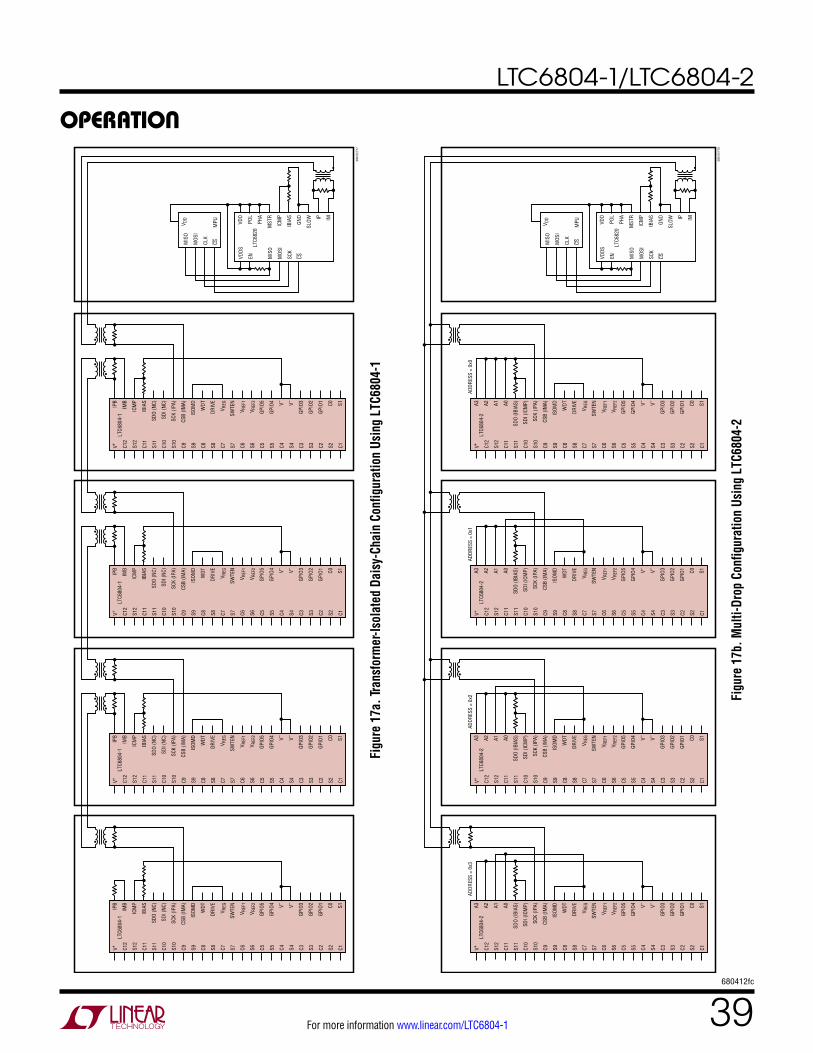
LTC6804-1/LTC6804-2
39680412fc
For more information www.linear.com/LTC6804-1
operaTion
6804
12 F
18
V+ C12
S12
C11
S11
C10
S10
C9 S9 C8 S8 C7 S7 C6 S6 C5 S5 C4 S4 C3 S3 C2 S2 C1
A3 A2 A1 A0
SDO
(IBIA
S)
SDI (
ICM
P)
SCK
(IPA)
CSB
(IMA)
ISOM
D
WDT
DRIV
E
V REG
SWTE
N
V REF
1
V REF
2
GPIO
5
GPIO
4 V– V–
GPIO
3
GPIO
2
GPIO
1 C0 S1
LTC6
804-
2
ADDR
ESS
= 0x
0V+ C1
2
S12
C11
S11
C10
S10
C9 S9 C8 S8 C7 S7 C6 S6 C5 S5 C4 S4 C3 S3 C2 S2 C1
A3 A2 A1 A0
SDO
(IBIA
S)
SDI (
ICM
P)
SCK
(IPA)
CSB
(IMA)
ISOM
D
WDT
DRIV
E
V REG
SWTE
N
V REF
1
V REF
2
GPIO
5
GPIO
4 V– V–
GPIO
3
GPIO
2
GPIO
1 C0 S1
LTC6
804-
2
ADDR
ESS
= 0x
1V+ C1
2
S12
C11
S11
C10
S10
C9 S9 C8 S8 C7 S7 C6 S6 C5 S5 C4 S4 C3 S3 C2 S2 C1
A3 A2 A1 A0
SDO
(IBIA
S)
SDI (
ICM
P)
SCK
(IPA)
CSB
(IMA)
ISOM
D
WDT
DRIV
E
V REG
SWTE
N
V REF
1
V REF
2
GPIO
5
GPIO
4 V– V–
GPIO
3
GPIO
2
GPIO
1 C0 S1
LTC6
804-
2
ADDR
ESS
= 0x
2V+ C1
2
S12
C11
S11
C10
S10
C9 S9 C8 S8 C7 S7 C6 S6 C5 S5 C4 S4 C3 S3 C2 S2 C1
A3 A2 A1 A0
SDO
(IBIA
S)
SDI (
ICM
P)
SCK
(IPA)
CSB
(IMA)
ISOM
D
WDT
DRIV
E
V REG
SWTE
N
V REF
1
V REF
2
GPIO
5
GPIO
4 V– V–
GPIO
3
GPIO
2
GPIO
1 C0 S1
LTC6
804-
2
ADDR
ESS
= 0x
3
••
••
••
••
VDDS
EN MIS
O
MOS
I
SCK
CS
VDD
POL
PHA
MST
R
ICM
P
IBIA
S
GND
SLOW IP IM
MIS
O
MOS
I
CLK
CS
V DD
MPU
LTC6
820
•
•
6804
12 F
17
VDDS
EN MIS
O
MOS
I
SCK
CS
VDD
POL
PHA
MST
R
ICM
P
IBIA
S
GND
SLOW IP IM
MIS
O
MOS
I
CLK
CS
V DD
MPU
LTC6
820
V+ C12
S12
C11
S11
C10
S10
C9 S9 C8 S8 C7 S7 C6 S6 C5 S5 C4 S4 C3 S3 C2 S2 C1
IPB
IMB
ICM
P
IBIA
S
SDO
(NC)
SDI (
NC)
SCK
(IPA)
CSB
(IMA)
ISOM
D
WDT
DRIV
E
V REG
SWTE
N
V REF
1
V REF
2
GPIO
5
GPIO
4 V– V–
GPIO
3
GPIO
2
GPIO
1 C0 S1
LTC6
804-
1V+ C1
2
S12
C11
S11
C10
S10
C9 S9 C8 S8 C7 S7 C6 S6 C5 S5 C4 S4 C3 S3 C2 S2 C1
IPB
IMB
ICM
P
IBIA
S
SDO
(NC)
SDI (
NC)
SCK
(IPA)
CSB
(IMA)
ISOM
D
WDT
DRIV
E
V REG
SWTE
N
V REF
1
V REF
2
GPIO
5
GPIO
4 V– V–
GPIO
3
GPIO
2
GPIO
1 C0 S1
LTC6
804-
1V+ C1
2
S12
C11
S11
C10
S10
C9 S9 C8 S8 C7 S7 C6 S6 C5 S5 C4 S4 C3 S3 C2 S2 C1
IPB
IMB
ICM
P
IBIA
S
SDO
(NC)
SDI (
NC)
SCK
(IPA)
CSB
(IMA)
ISOM
D
WDT
DRIV
E
V REG
SWTE
N
V REF
1
V REF
2
GPIO
5
GPIO
4 V– V–
GPIO
3
GPIO
2
GPIO
1 C0 S1
LTC6
804-
1V+ C1
2
S12
C11
S11
C10
S10
C9 S9 C8 S8 C7 S7 C6 S6 C5 S5 C4 S4 C3 S3 C2 S2 C1
IPB
IMB
ICM
P
IBIA
S
SDO
(NC)
SDI (
NC)
SCK
(IPA)
CSB
(IMA)
ISOM
D
WDT
DRIV
E
V REG
SWTE
N
V REF
1
V REF
2
GPIO
5
GPIO
4 V– V–
GPIO
3
GPIO
2
GPIO
1 C0 S1
LTC6
804-
1
••
••
••
••
••
••
••
•
•
Figu
re 1
7a. T
rans
form
er-Is
olat
ed D
aisy
-Cha
in C
onfig
urat
ion
Usin
g LT
C680
4-1
Figu
re 1
7b. M
ulti-
Drop
Con
figur
atio
n Us
ing
LTC6
804-
2
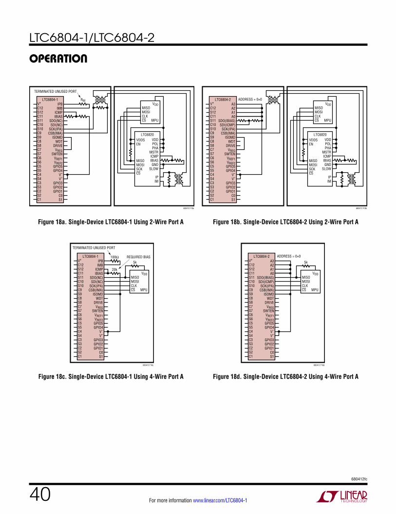
LTC6804-1/LTC6804-2
40680412fc
For more information www.linear.com/LTC6804-1
operaTion
Figure 18a. Single-Device LTC6804-1 Using 2-Wire Port A
Figure 18c. Single-Device LTC6804-1 Using 4-Wire Port A
Figure 18b. Single-Device LTC6804-2 Using 2-Wire Port A
Figure 18d. Single-Device LTC6804-2 Using 4-Wire Port A
•
•
••
680412 F18a
VDDSEN
MISOMOSISCKCS
VDDPOLPHA
MSTRICMPIBIASGND
SLOW
IPIM
MISOMOSICLKCS
VDD
MPU
LTC6820
V+
C12S12C11S11C10S10C9S9C8S8C7S7C6S6C5S5C4S4C3S3C2S2C1
IPBIMB
ICMPIBIAS
SDO(NC)SDI(NC)
SCK(IPA)CSB(IMA)
ISOMDWDT
DRIVEVREG
SWTENVREF1VREF2GPIO5GPIO4
V–
V–
GPIO3GPIO2GPIO1
C0S1
LTC6804-1
TERMINATED UNUSED PORT
RM •
•
••
680412 F18b
VDDSEN
MISOMOSISCKCS
VDDPOLPHA
MSTRICMPIBIASGND
SLOW
IPIM
MISOMOSICLKCS
VDD
MPU
LTC6820
V+
C12S12C11S11C10S10C9S9C8S8C7S7C6S6C5S5C4S4C3S3C2S2C1
A3A2A1A0
SDO(IBIAS)SDI(ICMP)
SCK(IPA)CSB(IMA)
ISOMDWDT
DRIVEVREG
SWTENVREF1VREF2GPIO5GPIO4
V–
V–
GPIO3GPIO2GPIO1
C0S1
LTC6804-2 ADDRESS = 0×0
680412 F18c
V+
C12S12C11S11C10S10C9S9C8S8C7S7C6S6C5S5C4S4C3S3C2S2C1
IPBIMB
ICMPIBIAS
SDO(NC)SDI(NC)
SCK(IPA)CSB(IMA)
ISOMDWDT
DRIVEVREG
SWTENVREF1VREF2GPIO5GPIO4
V–
V–
GPIO3GPIO2GPIO1
C0S1
LTC6804-1
TERMINATED UNUSED PORT
100Ω
20k
MISOMOSICLKCS
VDD
MPU
REQUIRED BIAS5k
680412 F18d
V+
C12S12C11S11C10S10C9S9C8S8C7S7C6S6C5S5C4S4C3S3C2S2C1
A3A2A1A0
SDO(IBIAS)SDI(ICMP)
SCK(IPA)CSB(IMA)
ISOMDWDT
DRIVEVREG
SWTENVREF1VREF2GPIO5GPIO4
V–
V–
GPIO3GPIO2GPIO1
C0S1
LTC6804-2 ADDRESS = 0×0
MISOMOSICLKCS
VDD
MPU
5k
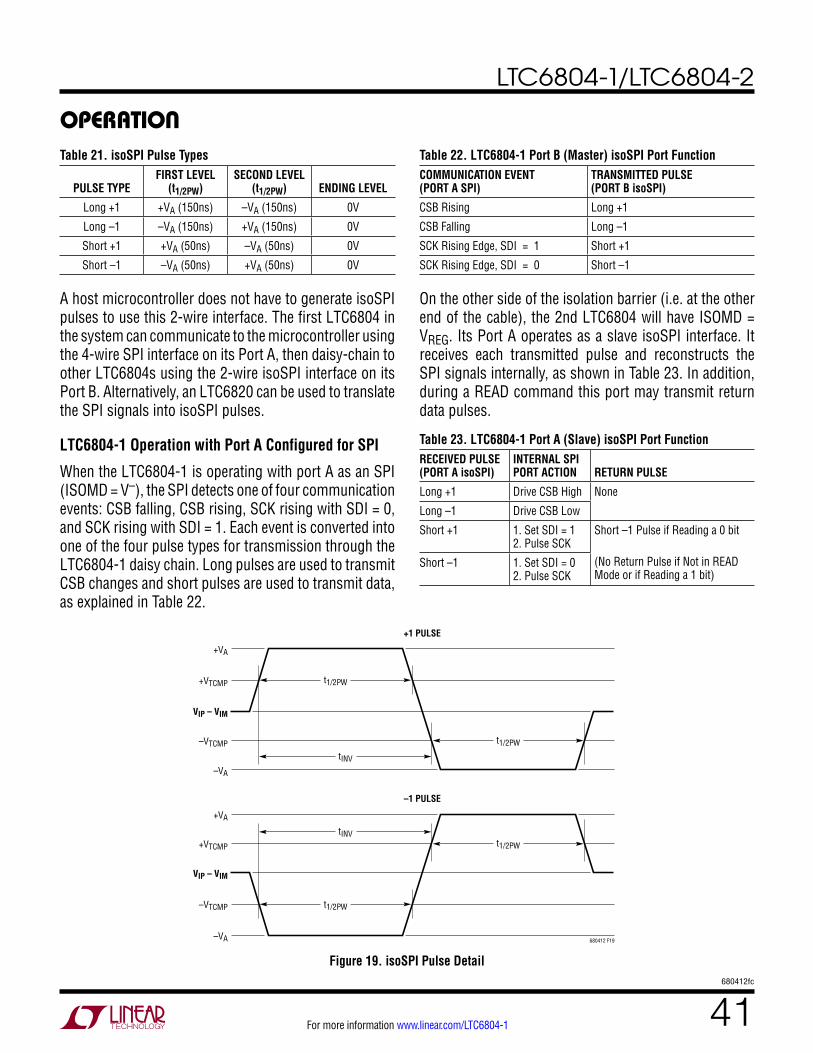
LTC6804-1/LTC6804-2
41680412fc
For more information www.linear.com/LTC6804-1
operaTionTable 21. isoSPI Pulse Types
PULSE TYPEFIRST LEVEL
(t1/2PW)SECOND LEVEL
(t1/2PW) ENDING LEVEL
Long +1 +VA (150ns) –VA (150ns) 0V
Long –1 –VA (150ns) +VA (150ns) 0V
Short +1 +VA (50ns) –VA (50ns) 0V
Short –1 –VA (50ns) +VA (50ns) 0V
A host microcontroller does not have to generate isoSPI pulses to use this 2-wire interface. The first LTC6804 in the system can communicate to the microcontroller using the 4-wire SPI interface on its Port A, then daisy-chain to other LTC6804s using the 2-wire isoSPI interface on its Port B. Alternatively, an LTC6820 can be used to translate the SPI signals into isoSPI pulses.
LTC6804-1 Operation with Port A Configured for SPI
When the LTC6804-1 is operating with port A as an SPI (ISOMD = V–), the SPI detects one of four communication events: CSB falling, CSB rising, SCK rising with SDI = 0, and SCK rising with SDI = 1. Each event is converted into one of the four pulse types for transmission through the LTC6804-1 daisy chain. Long pulses are used to transmit CSB changes and short pulses are used to transmit data, as explained in Table 22.
Table 22. LTC6804-1 Port B (Master) isoSPI Port FunctionCOMMUNICATION EVENT (PORT A SPI)
TRANSMITTED PULSE (PORT B isoSPI)
CSB Rising Long +1
CSB Falling Long –1
SCK Rising Edge, SDI = 1 Short +1
SCK Rising Edge, SDI = 0 Short –1
On the other side of the isolation barrier (i.e. at the other end of the cable), the 2nd LTC6804 will have ISOMD = VREG. Its Port A operates as a slave isoSPI interface. It receives each transmitted pulse and reconstructs the SPI signals internally, as shown in Table 23. In addition, during a READ command this port may transmit return data pulses.
Table 23. LTC6804-1 Port A (Slave) isoSPI Port FunctionRECEIVED PULSE (PORT A isoSPI)
INTERNAL SPI PORT ACTION RETURN PULSE
Long +1 Drive CSB High None
Long –1 Drive CSB Low
Short +1 1. Set SDI = 1 2. Pulse SCK
Short –1 Pulse if Reading a 0 bit (No Return Pulse if Not in READ Mode or if Reading a 1 bit)
Short –1 1. Set SDI = 0 2. Pulse SCK
Figure 19. isoSPI Pulse Detail
+VTCMP
+VA
–VTCMP
VIP – VIM
+1 PULSE
–VA
t1/2PW
tINV
t1/2PW
+VTCMP
+VA
–VTCMP
VIP – VIM
–VA
t1/2PW
tINVt1/2PW
680412 F19
–1 PULSE
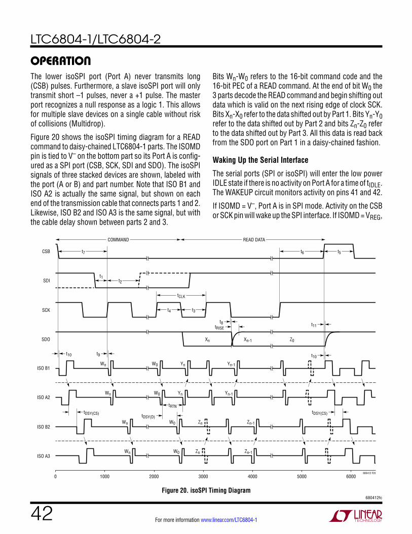
LTC6804-1/LTC6804-2
42680412fc
For more information www.linear.com/LTC6804-1
operaTion
Figure 20. isoSPI Timing Diagram
The lower isoSPI port (Port A) never transmits long (CSB) pulses. Furthermore, a slave isoSPI port will only transmit short –1 pulses, never a +1 pulse. The master port recognizes a null response as a logic 1. This allows for multiple slave devices on a single cable without risk of collisions (Multidrop).
Figure 20 shows the isoSPI timing diagram for a READ command to daisy-chained LTC6804-1 parts. The ISOMD pin is tied to V– on the bottom part so its Port A is config-ured as a SPI port (CSB, SCK, SDI and SDO). The isoSPI signals of three stacked devices are shown, labeled with the port (A or B) and part number. Note that ISO B1 and ISO A2 is actually the same signal, but shown on each end of the transmission cable that connects parts 1 and 2. Likewise, ISO B2 and ISO A3 is the same signal, but with the cable delay shown between parts 2 and 3.
Bits Wn-W0 refers to the 16-bit command code and the 16-bit PEC of a READ command. At the end of bit W0 the 3 parts decode the READ command and begin shifting out data which is valid on the next rising edge of clock SCK. Bits Xn-X0 refer to the data shifted out by Part 1. Bits Yn-Y0 refer to the data shifted out by Part 2 and bits Zn-Z0 refer to the data shifted out by Part 3. All this data is read back from the SDO port on Part 1 in a daisy-chained fashion.
Waking Up the Serial Interface
The serial ports (SPI or isoSPI) will enter the low power IDLE state if there is no activity on Port A for a time of tIDLE. The WAKEUP circuit monitors activity on pins 41 and 42.
If ISOMD = V–, Port A is in SPI mode. Activity on the CSB or SCK pin will wake up the SPI interface. If ISOMD = VREG,
680412 F20
SDI
SCK
SDO
CSB
ISO A2
ISO B2
ISO A3
ISO B1
READ DATACOMMAND
6000500040003000200010000
t7 t6 t5
tRTN
t11
t10
t2t1
tCLK
t4 t3
tRISE
tDSY(CS)
t8
t9
tDSY(CS)
Zn-1
Zn-1
Zn
Zn
W0
W0
Wn
Wn
Yn-1
Yn-1
Yn
Yn
W0
W0
Xn-1Xn Z0
Wn
Wn
tDSY(D)
t10
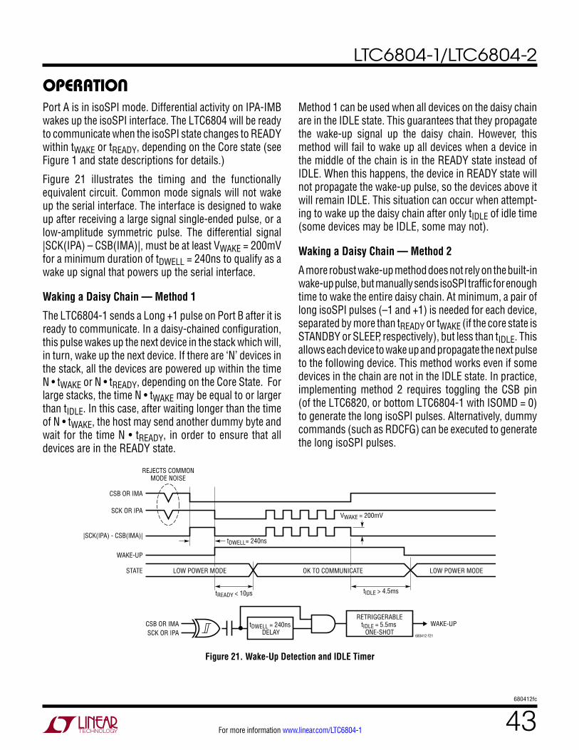
LTC6804-1/LTC6804-2
43680412fc
For more information www.linear.com/LTC6804-1
operaTionPort A is in isoSPI mode. Differential activity on IPA-IMB wakes up the isoSPI interface. The LTC6804 will be ready to communicate when the isoSPI state changes to READY within tWAKE or tREADY, depending on the Core state (see Figure 1 and state descriptions for details.)
Figure 21 illustrates the timing and the functionally equivalent circuit. Common mode signals will not wake up the serial interface. The interface is designed to wake up after receiving a large signal single-ended pulse, or a low-amplitude symmetric pulse. The differential signal |SCK(IPA) – CSB(IMA)|, must be at least VWAKE = 200mV for a minimum duration of tDWELL = 240ns to qualify as a wake up signal that powers up the serial interface.
Waking a Daisy Chain — Method 1
The LTC6804-1 sends a Long +1 pulse on Port B after it is ready to communicate. In a daisy-chained configuration, this pulse wakes up the next device in the stack which will, in turn, wake up the next device. If there are ‘N’ devices in the stack, all the devices are powered up within the time N • tWAKE or N • tREADY, depending on the Core State. For large stacks, the time N • tWAKE may be equal to or larger than tIDLE. In this case, after waiting longer than the time of N • tWAKE, the host may send another dummy byte and wait for the time N • tREADY, in order to ensure that all devices are in the READY state.
Method 1 can be used when all devices on the daisy chain are in the IDLE state. This guarantees that they propagate the wake-up signal up the daisy chain. However, this method will fail to wake up all devices when a device in the middle of the chain is in the READY state instead of IDLE. When this happens, the device in READY state will not propagate the wake-up pulse, so the devices above it will remain IDLE. This situation can occur when attempt-ing to wake up the daisy chain after only tIDLE of idle time (some devices may be IDLE, some may not).
Waking a Daisy Chain — Method 2
A more robust wake-up method does not rely on the built-in wake-up pulse, but manually sends isoSPI traffic for enough time to wake the entire daisy chain. At minimum, a pair of long isoSPI pulses (–1 and +1) is needed for each device, separated by more than tREADY or tWAKE (if the core state is STANDBY or SLEEP, respectively), but less than tIDLE. This allows each device to wake up and propagate the next pulse to the following device. This method works even if some devices in the chain are not in the IDLE state. In practice, implementing method 2 requires toggling the CSB pin (of the LTC6820, or bottom LTC6804-1 with ISOMD = 0) to generate the long isoSPI pulses. Alternatively, dummy commands (such as RDCFG) can be executed to generate the long isoSPI pulses.
Figure 21. Wake-Up Detection and IDLE Timer
680412 F21
CSB OR IMA
SCK OR IPA
|SCK(IPA) - CSB(IMA)|
WAKE-UP
STATE
REJECTS COMMONMODE NOISE
WAKE-UPCSB OR IMASCK OR IPA
LOW POWER MODE
tIDLE > 4.5mstREADY < 10µs
tDWELL= 240ns
VWAKE = 200mV
LOW POWER MODE OK TO COMMUNICATE
tDWELL = 240ns DELAY
RETRIGGERABLEtIDLE = 5.5ms
ONE-SHOT
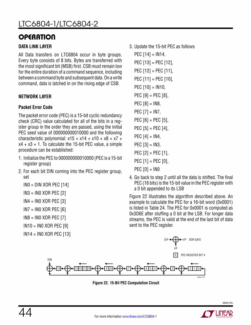
LTC6804-1/LTC6804-2
44680412fc
For more information www.linear.com/LTC6804-1
operaTionDATA LINK LAYER
All Data transfers on LTC6804 occur in byte groups. Every byte consists of 8 bits. Bytes are transferred with the most significant bit (MSB) first. CSB must remain low for the entire duration of a command sequence, including between a command byte and subsequent data. On a write command, data is latched in on the rising edge of CSB.
NETWORK LAYER
Packet Error Code
The packet error code (PEC) is a 15-bit cyclic redundancy check (CRC) value calculated for all of the bits in a reg-ister group in the order they are passed, using the initial PEC seed value of 000000000010000 and the following characteristic polynomial: x15 + x14 + x10 + x8 + x7 + x4 + x3 + 1. To calculate the 15-bit PEC value, a simple procedure can be established:
1. Initialize the PEC to 000000000010000 (PEC is a 15-bit register group)
2. For each bit DIN coming into the PEC register group, set
IN0 = DIN XOR PEC [14]
IN3 = IN0 XOR PEC [2]
IN4 = IN0 XOR PEC [3]
IN7 = IN0 XOR PEC [6]
IN8 = IN0 XOR PEC [7]
IN10 = IN0 XOR PEC [9]
IN14 = IN0 XOR PEC [13]
3. Update the 15-bit PEC as follows
PEC [14] = IN14,
PEC [13] = PEC [12],
PEC [12] = PEC [11],
PEC [11] = PEC [10],
PEC [10] = IN10,
PEC [9] = PEC [8],
PEC [8] = IN8,
PEC [7] = IN7,
PEC [6] = PEC [5],
PEC [5] = PEC [4],
PEC [4] = IN4,
PEC [3] = IN3,
PEC [2] = PEC [1],
PEC [1] = PEC [0],
PEC [0] = IN0
4. Go back to step 2 until all the data is shifted. The final PEC (16 bits) is the 15-bit value in the PEC register with a 0 bit appended to its LSB
Figure 22 illustrates the algorithm described above. An example to calculate the PEC for a 16-bit word (0x0001) is listed in Table 24. The PEC for 0x0001 is computed as 0x3D6E after stuffing a 0 bit at the LSB. For longer data streams, the PEC is valid at the end of the last bit of data sent to the PEC register.
Figure 22. 15-Bit PEC Computation Circuit
680412 F22
DIN
I/P
O/P I/P
PEC REGISTER BIT X
XOR GATE
X
012345678914 10111213
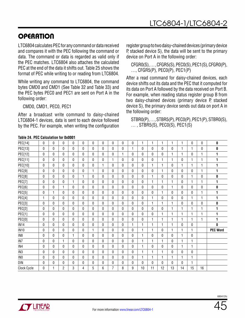
LTC6804-1/LTC6804-2
45680412fc
For more information www.linear.com/LTC6804-1
Table 24. PEC Calculation for 0x0001PEC[14] 0 0 0 0 0 0 0 0 0 0 1 1 1 1 1 0 0 0PEC[13] 0 0 0 0 0 0 0 0 0 1 0 0 0 0 1 1 0 0PEC[12] 0 0 0 0 0 0 0 0 1 0 0 0 0 1 1 0 1 1PEC[11] 0 0 0 0 0 0 0 1 0 0 0 0 1 1 0 1 1 1PEC[10] 0 0 0 0 0 0 1 0 0 0 0 1 1 0 1 1 1 1PEC[9] 0 0 0 0 0 1 0 0 0 0 0 0 1 0 0 0 1 1PEC[8] 0 0 0 0 1 0 0 0 0 0 0 1 0 0 0 1 0 0PEC[7] 0 0 0 1 0 0 0 0 0 0 0 1 1 1 0 1 1 1PEC[6] 0 0 1 0 0 0 0 0 0 0 0 0 0 1 0 0 0 0PEC[5] 0 1 0 0 0 0 0 0 0 0 0 0 1 0 0 0 1 1PEC[4] 1 0 0 0 0 0 0 0 0 0 0 1 0 0 0 1 1 1PEC[3] 0 0 0 0 0 0 0 0 0 0 0 1 1 1 0 0 0 0PEC[2] 0 0 0 0 0 0 0 0 0 0 0 0 0 1 1 1 1 1PEC[1] 0 0 0 0 0 0 0 0 0 0 0 0 1 1 1 1 1 1PEC[0] 0 0 0 0 0 0 0 0 0 0 0 1 1 1 1 1 1 1IN14 0 0 0 0 0 0 0 0 0 1 1 1 1 1 0 0 0IN10 0 0 0 0 0 1 0 0 0 0 1 1 0 1 1 1 PEC WordIN8 0 0 0 1 0 0 0 0 0 0 1 0 0 0 1 0IN7 0 0 1 0 0 0 0 0 0 0 1 1 1 0 1 1IN4 0 0 0 0 0 0 0 0 0 0 1 0 0 0 1 1IN3 0 0 0 0 0 0 0 0 0 0 1 1 1 0 0 0IN0 0 0 0 0 0 0 0 0 0 0 1 1 1 1 1 1DIN 0 0 0 0 0 0 0 0 0 0 0 0 0 0 0 1Clock Cycle 0 1 2 3 4 5 6 7 8 9 10 11 12 13 14 15 16
operaTionLTC6804 calculates PEC for any command or data received and compares it with the PEC following the command or data. The command or data is regarded as valid only if the PEC matches. LTC6804 also attaches the calculated PEC at the end of the data it shifts out. Table 25 shows the format of PEC while writing to or reading from LTC6804.
While writing any command to LTC6804, the command bytes CMD0 and CMD1 (See Table 32 and Table 33) and the PEC bytes PEC0 and PEC1 are sent on Port A in the following order:
CMD0, CMD1, PEC0, PEC1
After a broadcast write command to daisy-chained LTC6804-1 devices, data is sent to each device followed by the PEC. For example, when writing the configuration
register group to two daisy-chained devices (primary device P, stacked device S), the data will be sent to the primary device on Port A in the following order:
CFGR0(S), … , CFGR5(S), PEC0(S), PEC1(S), CFGR0(P), …, CFGR5(P), PEC0(P), PEC1(P)
After a read command for daisy-chained devices, each device shifts out its data and the PEC that it computed for its data on Port A followed by the data received on Port B. For example, when reading status register group B from two daisy-chained devices (primary device P, stacked device S), the primary device sends out data on port A in the following order:
STBR0(P), …, STBR5(P), PEC0(P), PEC1(P), STBR0(S), … , STBR5(S), PEC0(S), PEC1(S)
LTC6804-1/LTC6804-2
46680412fc
For more information www.linear.com/LTC6804-1
Table 25. Write/Read PEC Format NAME RD/WR BIT 7 BIT 6 BIT 5 BIT 4 BIT 3 BIT 2 BIT 1 BIT 0
PEC0 RD/WR PEC[14] PEC[13] PEC[12] PEC[11] PEC[10] PEC[9] PEC[8] PEC[7]
PEC1 RD/WR PEC[6] PEC[5] PEC[4] PEC[3] PEC[2] PEC[1] PEC[0] 0
operaTion
Daisy-chained (LTC6804-1) configurations support broad-cast commands only, because they have no addressing. All devices in the chain receive the command bytes simul-taneously. For example, to initiate ADC conversions in a stack of devices, a single ADCV command is sent, and all devices will start conversions at the same time. For read and write commands, a single command is sent, and then the stacked devices effectively turn into a cascaded shift register, in which data is shifted through each device to the next device in the stack. See the Serial Programming Examples section.
Polling Methods
The simplest method to determine ADC completion is for the controller to start an ADC conversion and wait for the specified conversion time to pass before reading the results. Polling is not supported with daisy-chain com-munication (LTC6804-1).
In parallel configurations that communicate in SPI mode (ISOMD pin tied low), there are two methods of poll-ing. The first method is to hold CSB low after an ADC conversion command is sent. After entering a conversion command, the SDO line is driven low when the device is busy performing conversions (Figure 23). SDO is pulled high when the device completes conversions. However, the SDO will also go back high when CSB goes high even if the device has not completed the conversion. An addressed device drives the SDO line based on its status alone. A problem with this method is that the controller is not free to do other serial communication while waiting for ADC conversions to complete.
The next method overcomes this limitation. The controller can send an ADC start command, perform other tasks, and then send a poll ADC converter status (PLADC) command to determine the status of the ADC conversions (Figure 24). After entering the PLADC command, SDO will go low if the device is busy performing conversions. SDO is pulled high at the end of conversions. However, the SDO will also
Broadcast vs Address CommandsCONFIGURATION TYPE OF COMMAND
DEVICE INTERFACE READ WRITE POLL
LTC6804-2(Address/Parallel)
SPI Address-Only
Address or
Broadcast
Address or
Broadcast
isoSPI Address-Only†
LTC6804-1(Daisy-Chain)
SPI or isoSPI
Broadcast-Only N/A
†The LTC6804-2 will not return data pulses when using broadcast commands in isoSPI mode. Therefore, ADC commands will execute, but polling will not work.
Address Commands (LTC6804-2 Only)
An address command is one in which only the addressed device on the bus responds. Address commands are used only with LTC6804-2 parts. All commands are compatible with addressing. See Bus Protocols for Address command format.
Broadcast Commands (LTC6804-1 or LTC6804-2)
A broadcast command is one to which all devices on the bus will respond, regardless of device address. This com-mand format can be used with LTC6804-1 and LTC6804-2 parts. See Bus Protocols for Broadcast command format. With broadcast commands all devices can be sent com-mands simultaneously.
In parallel (LTC6804-2) configurations, broadcast com-mands are useful for initiating ADC conversions or for sending write commands when all parts are being written with the same data. The polling function (automatic at the end of ADC commands, or manual using the PLADC com-mand) can also be used with broadcast commands, but only with parallel SPI interfaces. Polling is not compatible with parallel isoSPI. Likewise, broadcast read commands should not be used in a parallel configuration (either SPI or isoSPI).
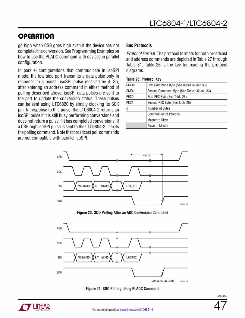
LTC6804-1/LTC6804-2
47680412fc
For more information www.linear.com/LTC6804-1
operaTiongo high when CSB goes high even if the device has not completed the conversion. See Programming Examples on how to use the PLADC command with devices in parallel configuration.
In parallel configurations that communicate in isoSPI mode, the low side port transmits a data pulse only in response to a master isoSPI pulse received by it. So, after entering an address command in either method of polling described above, isoSPI data pulses are sent to the part to update the conversion status. These pulses can be sent using LTC6820 by simply clocking its SCK pin. In response to this pulse, the LTC6804-2 returns an isoSPI pulse if it is still busy performing conversions and does not return a pulse if it has completed conversions. If a CSB high isoSPI pulse is sent to the LTC6804-2, it exits the polling command. Note that broadcast poll commands are not compatible with parallel isoSPI.
Bus Protocols
Protocol Format: The protocol formats for both broadcast and address commands are depicted in Table 27 through Table 31. Table 26 is the key for reading the protocol diagrams.
Table 26. Protocol KeyCMD0 First Command Byte (See Tables 32 and 33)
CMD1 Second Command Byte (See Tables 32 and 33)
PEC0 First PEC Byte (See Table 25)
PEC1 Second PEC Byte (See Table 25)
n Number of Bytes
… Continuation of Protocol
Master to Slave
Slave to Master
Figure 23. SDO Polling After an ADC Conversion Command
Figure 24. SDO Polling Using PLADC Command
680412 F23
SDI
SCK
tCYCLE
SDO
CSB
MSB(CMD) LSB(PEC)BIT 14(CMD)
680412 F24
SDI
SCK
SDO
CSB
MSB(CMD) LSB(PEC)
CONVERSION DONE
BIT 14(CMD)
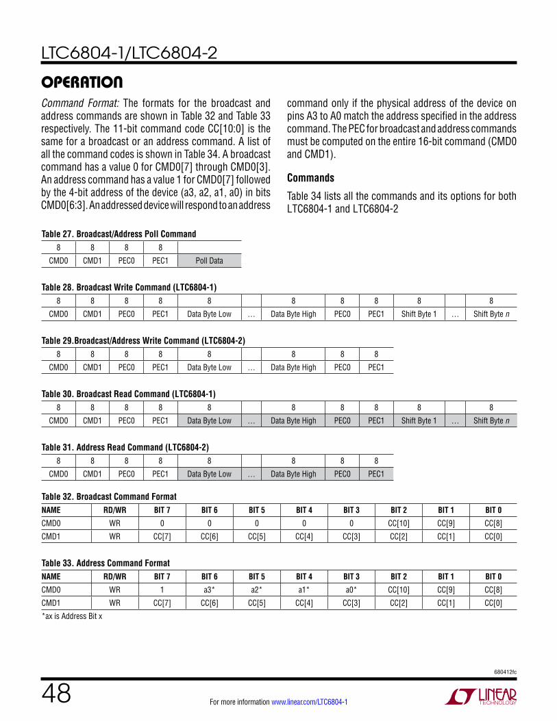
LTC6804-1/LTC6804-2
48680412fc
For more information www.linear.com/LTC6804-1
operaTion
Table 27. Broadcast/Address Poll Command8 8 8 8
CMD0 CMD1 PEC0 PEC1 Poll Data
Table 28. Broadcast Write Command (LTC6804-1)8 8 8 8 8 8 8 8 8 8
CMD0 CMD1 PEC0 PEC1 Data Byte Low … Data Byte High PEC0 PEC1 Shift Byte 1 … Shift Byte n
Table 29.Broadcast/Address Write Command (LTC6804-2)8 8 8 8 8 8 8 8
CMD0 CMD1 PEC0 PEC1 Data Byte Low … Data Byte High PEC0 PEC1
Table 30. Broadcast Read Command (LTC6804-1)8 8 8 8 8 8 8 8 8 8
CMD0 CMD1 PEC0 PEC1 Data Byte Low … Data Byte High PEC0 PEC1 Shift Byte 1 … Shift Byte n
Table 31. Address Read Command (LTC6804-2)8 8 8 8 8 8 8 8
CMD0 CMD1 PEC0 PEC1 Data Byte Low … Data Byte High PEC0 PEC1
Table 32. Broadcast Command FormatNAME RD/WR BIT 7 BIT 6 BIT 5 BIT 4 BIT 3 BIT 2 BIT 1 BIT 0
CMD0 WR 0 0 0 0 0 CC[10] CC[9] CC[8]
CMD1 WR CC[7] CC[6] CC[5] CC[4] CC[3] CC[2] CC[1] CC[0]
Table 33. Address Command FormatNAME RD/WR BIT 7 BIT 6 BIT 5 BIT 4 BIT 3 BIT 2 BIT 1 BIT 0
CMD0 WR 1 a3* a2* a1* a0* CC[10] CC[9] CC[8]
CMD1 WR CC[7] CC[6] CC[5] CC[4] CC[3] CC[2] CC[1] CC[0]
*ax is Address Bit x
Command Format: The formats for the broadcast and address commands are shown in Table 32 and Table 33 respectively. The 11-bit command code CC[10:0] is the same for a broadcast or an address command. A list of all the command codes is shown in Table 34. A broadcast command has a value 0 for CMD0[7] through CMD0[3]. An address command has a value 1 for CMD0[7] followed by the 4-bit address of the device (a3, a2, a1, a0) in bits CMD0[6:3]. An addressed device will respond to an address
command only if the physical address of the device on pins A3 to A0 match the address specified in the address command. The PEC for broadcast and address commands must be computed on the entire 16-bit command (CMD0 and CMD1).
Commands
Table 34 lists all the commands and its options for both LTC6804-1 and LTC6804-2
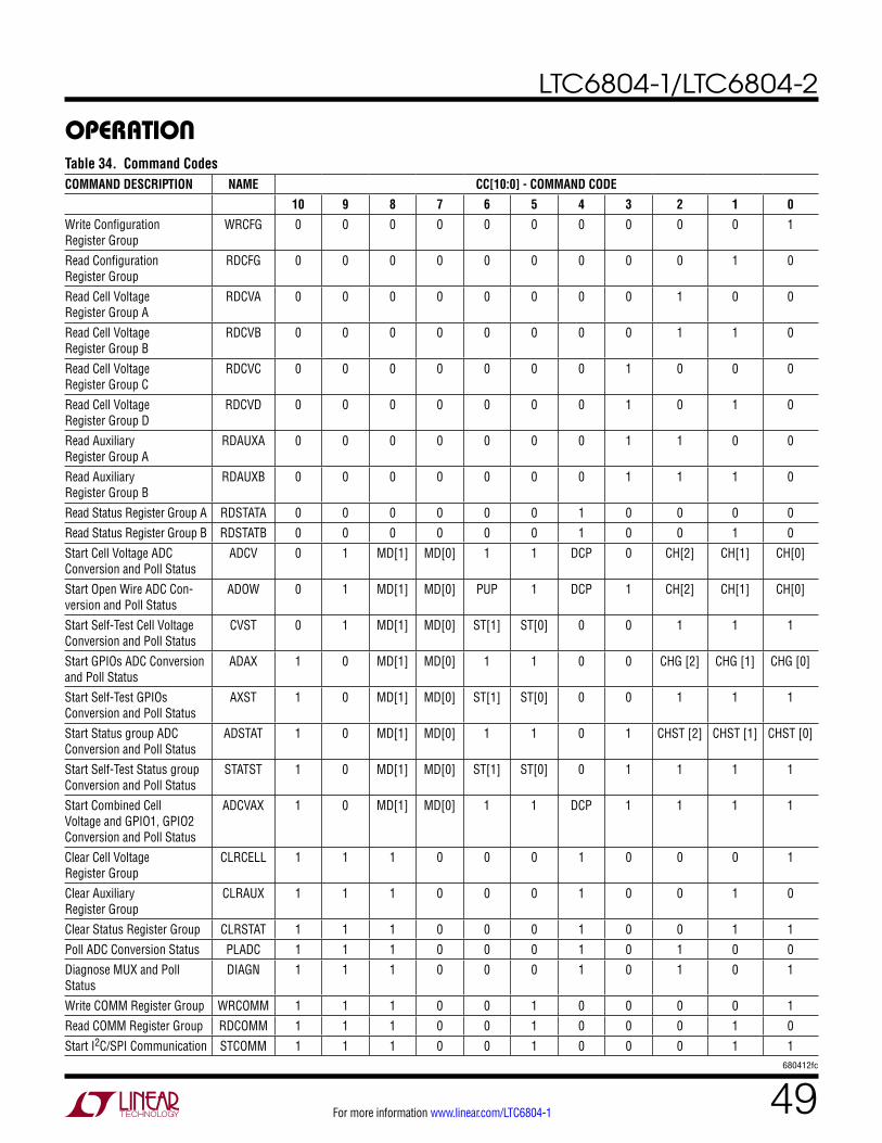
LTC6804-1/LTC6804-2
49680412fc
For more information www.linear.com/LTC6804-1
operaTionTable 34. Command CodesCOMMAND DESCRIPTION NAME CC[10:0] - COMMAND CODE
10 9 8 7 6 5 4 3 2 1 0Write Configuration Register Group
WRCFG 0 0 0 0 0 0 0 0 0 0 1
Read Configuration Register Group
RDCFG 0 0 0 0 0 0 0 0 0 1 0
Read Cell Voltage Register Group A
RDCVA 0 0 0 0 0 0 0 0 1 0 0
Read Cell Voltage Register Group B
RDCVB 0 0 0 0 0 0 0 0 1 1 0
Read Cell Voltage Register Group C
RDCVC 0 0 0 0 0 0 0 1 0 0 0
Read Cell Voltage Register Group D
RDCVD 0 0 0 0 0 0 0 1 0 1 0
Read Auxiliary Register Group A
RDAUXA 0 0 0 0 0 0 0 1 1 0 0
Read Auxiliary Register Group B
RDAUXB 0 0 0 0 0 0 0 1 1 1 0
Read Status Register Group A RDSTATA 0 0 0 0 0 0 1 0 0 0 0
Read Status Register Group B RDSTATB 0 0 0 0 0 0 1 0 0 1 0
Start Cell Voltage ADC Conversion and Poll Status
ADCV 0 1 MD[1] MD[0] 1 1 DCP 0 CH[2] CH[1] CH[0]
Start Open Wire ADC Con-version and Poll Status
ADOW 0 1 MD[1] MD[0] PUP 1 DCP 1 CH[2] CH[1] CH[0]
Start Self-Test Cell Voltage Conversion and Poll Status
CVST 0 1 MD[1] MD[0] ST[1] ST[0] 0 0 1 1 1
Start GPIOs ADC Conversion and Poll Status
ADAX 1 0 MD[1] MD[0] 1 1 0 0 CHG [2] CHG [1] CHG [0]
Start Self-Test GPIOs Conversion and Poll Status
AXST 1 0 MD[1] MD[0] ST[1] ST[0] 0 0 1 1 1
Start Status group ADC Conversion and Poll Status
ADSTAT 1 0 MD[1] MD[0] 1 1 0 1 CHST [2] CHST [1] CHST [0]
Start Self-Test Status group Conversion and Poll Status
STATST 1 0 MD[1] MD[0] ST[1] ST[0] 0 1 1 1 1
Start Combined Cell Voltage and GPIO1, GPIO2 Conversion and Poll Status
ADCVAX 1 0 MD[1] MD[0] 1 1 DCP 1 1 1 1
Clear Cell Voltage Register Group
CLRCELL 1 1 1 0 0 0 1 0 0 0 1
Clear Auxiliary Register Group
CLRAUX 1 1 1 0 0 0 1 0 0 1 0
Clear Status Register Group CLRSTAT 1 1 1 0 0 0 1 0 0 1 1
Poll ADC Conversion Status PLADC 1 1 1 0 0 0 1 0 1 0 0
Diagnose MUX and Poll Status
DIAGN 1 1 1 0 0 0 1 0 1 0 1
Write COMM Register Group WRCOMM 1 1 1 0 0 1 0 0 0 0 1
Read COMM Register Group RDCOMM 1 1 1 0 0 1 0 0 0 1 0
Start I2C/SPI Communication STCOMM 1 1 1 0 0 1 0 0 0 1 1
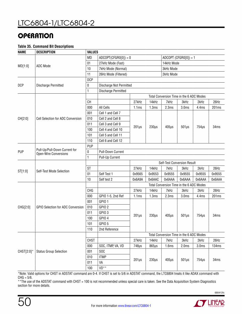
LTC6804-1/LTC6804-2
50680412fc
For more information www.linear.com/LTC6804-1
operaTionTable 35. Command Bit DescriptionsNAME DESCRIPTION VALUES
MD[1:0] ADC Mode
MD ADCOPT(CFGR0[0]) = 0 ADCOPT (CFGR0[0]) = 1
01 27kHz Mode (Fast) 14kHz Mode
10 7kHz Mode (Normal) 3kHz Mode
11 26Hz Mode (Filtered) 2kHz Mode
DCP Discharge Permitted
DCP
0 Discharge Not Permitted
1 Discharge Permitted
CH[2:0] Cell Selection for ADC Conversion
Total Conversion Time in the 6 ADC Modes
CH 27kHz 14kHz 7kHz 3kHz 2kHz 26Hz
000 All Cells 1.1ms 1.3ms 2.3ms 3.0ms 4.4ms 201ms
001 Cell 1 and Cell 7
201µs 230µs 405µs 501µs 754µs 34ms
010 Cell 2 and Cell 8
011 Cell 3 and Cell 9
100 Cell 4 and Cell 10
101 Cell 5 and Cell 11
110 Cell 6 and Cell 12
PUP Pull-Up/Pull-Down Current for Open-Wire Conversions
PUP
0 Pull-Down Current
1 Pull-Up Current
ST[1:0] Self-Test Mode Selection
Self-Test Conversion Result
ST 27kHz 14kHz 7kHz 3kHz 2kHz 26Hz
01 Self Test 1 0x9565 0x9553 0x9555 0x9555 0x9555 0x9555
10 Self test 2 0x6A9A 0x6AAC 0x6AAA 0x6AAA 0x6AAA 0x6AAA
CHG[2:0] GPIO Selection for ADC Conversion
Total Conversion Time in the 6 ADC Modes
CHG 27kHz 14kHz 7kHz 3kHz 2kHz 26Hz
000 GPIO 1-5, 2nd Ref 1.1ms 1.3ms 2.3ms 3.0ms 4.4ms 201ms
001 GPIO 1
201µs 230µs 405µs 501µs 754µs 34ms
010 GPIO 2
011 GPIO 3
100 GPIO 4
101 GPIO 5
110 2nd Reference
CHST[2:0]* Status Group Selection
Total Conversion Time in the 6 ADC Modes
CHST 27kHz 14kHz 7kHz 3kHz 2kHz 26Hz
000 SOC, ITMP, VA, VD 748µs 865µs 1.6ms 2.0ms 3.0ms 134ms
001 SOC
201µs 230µs 405µs 501µs 754µs 34ms010 ITMP
011 VA
100 VD**
*Note: Valid options for CHST in ADSTAT command are 0-4. If CHST is set to 5/6 in ADSTAT command, the LTC6804 treats it like ADAX command with CHG = 5/6. **The use of the ADSTAT command with CHST = 100 is not recommended unless special care is taken. See the Data Acquisition System Diagnostics section for more details.
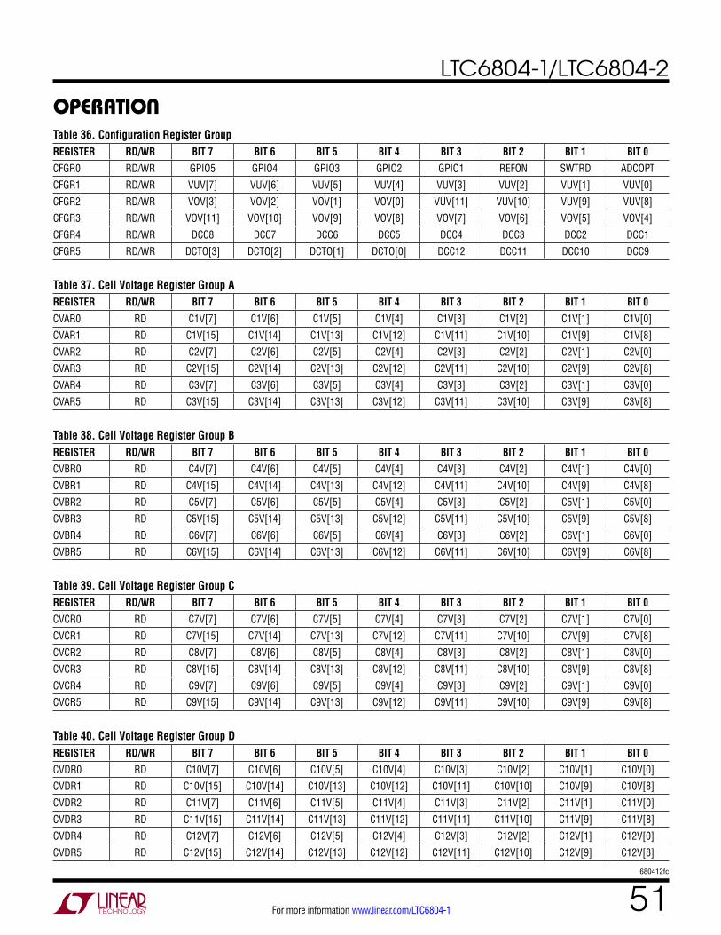
LTC6804-1/LTC6804-2
51680412fc
For more information www.linear.com/LTC6804-1
operaTionTable 36. Configuration Register GroupREGISTER RD/WR BIT 7 BIT 6 BIT 5 BIT 4 BIT 3 BIT 2 BIT 1 BIT 0
CFGR0 RD/WR GPIO5 GPIO4 GPIO3 GPIO2 GPIO1 REFON SWTRD ADCOPT
CFGR1 RD/WR VUV[7] VUV[6] VUV[5] VUV[4] VUV[3] VUV[2] VUV[1] VUV[0]
CFGR2 RD/WR VOV[3] VOV[2] VOV[1] VOV[0] VUV[11] VUV[10] VUV[9] VUV[8]
CFGR3 RD/WR VOV[11] VOV[10] VOV[9] VOV[8] VOV[7] VOV[6] VOV[5] VOV[4]
CFGR4 RD/WR DCC8 DCC7 DCC6 DCC5 DCC4 DCC3 DCC2 DCC1
CFGR5 RD/WR DCTO[3] DCTO[2] DCTO[1] DCTO[0] DCC12 DCC11 DCC10 DCC9
Table 37. Cell Voltage Register Group AREGISTER RD/WR BIT 7 BIT 6 BIT 5 BIT 4 BIT 3 BIT 2 BIT 1 BIT 0
CVAR0 RD C1V[7] C1V[6] C1V[5] C1V[4] C1V[3] C1V[2] C1V[1] C1V[0]
CVAR1 RD C1V[15] C1V[14] C1V[13] C1V[12] C1V[11] C1V[10] C1V[9] C1V[8]
CVAR2 RD C2V[7] C2V[6] C2V[5] C2V[4] C2V[3] C2V[2] C2V[1] C2V[0]
CVAR3 RD C2V[15] C2V[14] C2V[13] C2V[12] C2V[11] C2V[10] C2V[9] C2V[8]
CVAR4 RD C3V[7] C3V[6] C3V[5] C3V[4] C3V[3] C3V[2] C3V[1] C3V[0]
CVAR5 RD C3V[15] C3V[14] C3V[13] C3V[12] C3V[11] C3V[10] C3V[9] C3V[8]
Table 38. Cell Voltage Register Group BREGISTER RD/WR BIT 7 BIT 6 BIT 5 BIT 4 BIT 3 BIT 2 BIT 1 BIT 0
CVBR0 RD C4V[7] C4V[6] C4V[5] C4V[4] C4V[3] C4V[2] C4V[1] C4V[0]
CVBR1 RD C4V[15] C4V[14] C4V[13] C4V[12] C4V[11] C4V[10] C4V[9] C4V[8]
CVBR2 RD C5V[7] C5V[6] C5V[5] C5V[4] C5V[3] C5V[2] C5V[1] C5V[0]
CVBR3 RD C5V[15] C5V[14] C5V[13] C5V[12] C5V[11] C5V[10] C5V[9] C5V[8]
CVBR4 RD C6V[7] C6V[6] C6V[5] C6V[4] C6V[3] C6V[2] C6V[1] C6V[0]
CVBR5 RD C6V[15] C6V[14] C6V[13] C6V[12] C6V[11] C6V[10] C6V[9] C6V[8]
Table 39. Cell Voltage Register Group CREGISTER RD/WR BIT 7 BIT 6 BIT 5 BIT 4 BIT 3 BIT 2 BIT 1 BIT 0
CVCR0 RD C7V[7] C7V[6] C7V[5] C7V[4] C7V[3] C7V[2] C7V[1] C7V[0]
CVCR1 RD C7V[15] C7V[14] C7V[13] C7V[12] C7V[11] C7V[10] C7V[9] C7V[8]
CVCR2 RD C8V[7] C8V[6] C8V[5] C8V[4] C8V[3] C8V[2] C8V[1] C8V[0]
CVCR3 RD C8V[15] C8V[14] C8V[13] C8V[12] C8V[11] C8V[10] C8V[9] C8V[8]
CVCR4 RD C9V[7] C9V[6] C9V[5] C9V[4] C9V[3] C9V[2] C9V[1] C9V[0]
CVCR5 RD C9V[15] C9V[14] C9V[13] C9V[12] C9V[11] C9V[10] C9V[9] C9V[8]
Table 40. Cell Voltage Register Group DREGISTER RD/WR BIT 7 BIT 6 BIT 5 BIT 4 BIT 3 BIT 2 BIT 1 BIT 0
CVDR0 RD C10V[7] C10V[6] C10V[5] C10V[4] C10V[3] C10V[2] C10V[1] C10V[0]
CVDR1 RD C10V[15] C10V[14] C10V[13] C10V[12] C10V[11] C10V[10] C10V[9] C10V[8]
CVDR2 RD C11V[7] C11V[6] C11V[5] C11V[4] C11V[3] C11V[2] C11V[1] C11V[0]
CVDR3 RD C11V[15] C11V[14] C11V[13] C11V[12] C11V[11] C11V[10] C11V[9] C11V[8]
CVDR4 RD C12V[7] C12V[6] C12V[5] C12V[4] C12V[3] C12V[2] C12V[1] C12V[0]
CVDR5 RD C12V[15] C12V[14] C12V[13] C12V[12] C12V[11] C12V[10] C12V[9] C12V[8]

LTC6804-1/LTC6804-2
52680412fc
For more information www.linear.com/LTC6804-1
Table 41. Auxiliary Register Group AREGISTER RD/WR BIT 7 BIT 6 BIT 5 BIT 4 BIT 3 BIT 2 BIT 1 BIT 0
AVAR0 RD G1V[7] G1V[6] G1V[5] G1V[4] G1V[3] G1V[2] G1V[1] G1V[0]
AVAR1 RD G1V[15] G1V[14] G1V[13] G1V[12] G1V[11] G1V[10] G1V[9] G1V[8]
AVAR2 RD G2V[7] G2V[6] G2V[5] G2V[4] G2V[3] G2V[2] G2V[1] G2V[0]
AVAR3 RD G2V[15] G2V[14] G2V[13] G2V[12] G2V[11] G2V[10] G2V[9] G2V[8]
AVAR4 RD G3V[7] G3V[6] G3V[5] G3V[4] G3V[3] G3V[2] G3V[1] G3V[0]
AVAR5 RD G3V[15] G3V[14] G3V[13] G3V[12] G3V[11] G3V[10] G3V[9] G3V[8]
Table 42. Auxiliary Register Group BREGISTER RD/WR BIT 7 BIT 6 BIT 5 BIT 4 BIT 3 BIT 2 BIT 1 BIT 0
AVBR0 RD G4V[7] G4V[6] G4V[5] G4V[4] G4V[3] G4V[2] G4V[1] G4V[0]
AVBR1 RD G4V[15] G4V[14] G4V[13] G4V[12] G4V[11] G4V[10] G4V[9] G4V[8]
AVBR2 RD G5V[7] G5V[6] G5V[5] G5V[4] G5V[3] G5V[2] G5V[1] G5V[0]
AVBR3 RD G5V[15] G5V[14] G5V[13] G5V[12] G5V[11] G5V[10] G5V[9] G5V[8]
AVBR4 RD REF[7] REF[6] REF[5] REF[4] REF[3] REF[2] REF[1] REF[0]
AVBR5 RD REF[15] REF[14] REF[13] REF[12] REF[11] REF[10] REF[9] REF[8]
Table 43. Status Register Group AREGISTER RD/WR BIT 7 BIT 6 BIT 5 BIT 4 BIT 3 BIT 2 BIT 1 BIT 0
STAR0 RD SOC[7] SOC[6] SOC[5] SOC[4] SOC[3] SOC[2] SOC[1] SOC[0]
STAR1 RD SOC[15] SOC[14] SOC[13] SOC[12] SOC[11] SOC[10] SOC[9] SOC[8]
STAR2 RD ITMP[7] ITMP[6] ITMP[5] ITMP[4] ITMP[3] ITMP[2] ITMP[1] ITMP[0]
STAR3 RD ITMP[15] ITMP[14] ITMP[13] ITMP[12] ITMP[11] ITMP[10] ITMP[9] ITMP[8]
STAR4 RD VA[7] VA[6] VA[5] VA[4] VA[3] VA[2] VA[1] VA[0]
STAR5 RD VA[15] VA[14] VA[13] VA[12] VA[11] VA[10] VA[9] VA[8]
Table 44. Status Register Group BREGISTER RD/WR BIT 7 BIT 6 BIT 5 BIT 4 BIT 3 BIT 2 BIT 1 BIT 0
STBR0 RD VD[7] VD[6] VD[5] VD[4] VD[3] VD[2] VD[1] VD[0]
STBR1 RD VD[15] VD[14] VD[13] VD[12] VD[11] VD[10] VD[9] VD[8]
STBR2 RD C4OV C4UV C3OV C3UV C2OV C2UV C1OV C1UV
STBR3 RD C8OV C8UV C7OV C7UV C6OV C6UV C5OV C5UV
STBR4 RD C12OV C12UV C11OV C11UV C10OV C10UV C9OV C9UV
STBR5 RD REV[3] REV[2] REV[1] REV[0] RSVD RSVD MUXFAIL THSD
Table 45. COMM Register GroupREGISTER RD/WR BIT 7 BIT 6 BIT 5 BIT 4 BIT 3 BIT 2 BIT 1 BIT 0
COMM0 RD/WR ICOM0[3] ICOM0[2] ICOM0[1] ICOM0[0] D0[7] D0[6] D0[5] D0[4]
COMM1 RD/WR D0[3] D0[2] D0[1] D0[0] FCOM0[3] FCOM0[2] FCOM0[1] FCOM0[0]
COMM2 RD/WR ICOM1[3] ICOM1[2] ICOM1[1] ICOM1[0] D1[7] D1[6] D1[5] D1[4]
COMM3 RD/WR D1[3] D1[2] D1[1] D1[0] FCOM1[3] FCOM1[2] FCOM1[1] FCOM1[0]
COMM4 RD/WR ICOM2[3] ICOM2[2] ICOM2[1] ICOM2[0] D2[7] D2[6] D2[5] D2[4]
COMM5 RD/WR D2[3] D2[2] D2[1] D2[0] FCOM2[3] FCOM2[2] FCOM2[1] FCOM2[0]
operaTion
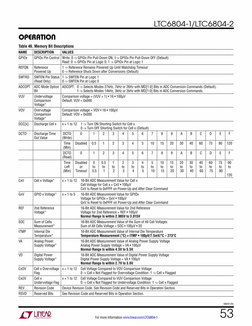
LTC6804-1/LTC6804-2
53680412fc
For more information www.linear.com/LTC6804-1
operaTionTable 46. Memory Bit Descriptions NAME DESCRIPTION VALUESGPIOx GPIOx Pin Control Write: 0 -> GPIOx Pin Pull-Down ON; 1-> GPIOx Pin Pull-Down OFF (Default)
Read: 0 -> GPIOx Pin at Logic 0; 1 -> GPIOx Pin at Logic 1REFON Reference
Powered Up1 -> Reference Remains Powered Up Until Watchdog Timeout 0 -> Reference Shuts Down after Conversions (Default)
SWTRD SWTEN Pin Status (Read Only)
1 -> SWTEN Pin at Logic 1 0 -> SWTEN Pin at Logic 0
ADCOPT ADC Mode Option Bit
ADCOPT: 0 -> Selects Modes 27kHz, 7kHz or 26Hz with MD[1:0] Bits in ADC Conversion Commands (Default). 1 -> Selects Modes 14kHz, 3kHz or 2kHz with MD[1:0] Bits in ADC Conversion Commands.
VUV Undervoltage Comparison Voltage*
Comparison voltage = (VUV + 1) • 16 • 100µV Default: VUV = 0x000
VOV Overvoltage Comparison Voltage*
Comparison voltage = VOV • 16 • 100µV Default: VOV = 0x000
DCC[x] Discharge Cell x x = 1 to 12 1 -> Turn ON Shorting Switch for Cell x 0 -> Turn OFF Shorting Switch for Cell x (Default)
DCTO Discharge Time Out Value
DCTO (Write)
0 1 2 3 4 5 6 7 8 9 A B C D E F
Time (Min)
Disabled 0.5 1 2 3 4 5 10 15 20 30 40 60 75 90 120
DCTO (Read)
0 1 2 3 4 5 6 7 8 9 A B C D E F
Time Left
(Min)
Disabled or
Timeout
0 to
0.5
0.5 to 1
1 to 2
2 to 3
3 to 4
4 to 5
5 to 10
10 to 15
15 to 20
20 to 30
30 to 40
40 to 60
60 to 75
75 to 90
90 to
120CxV Cell x Voltage* x = 1 to 12 16-Bit ADC Measurement Value for Cell x
Cell Voltage for Cell x = CxV • 100µV CxV Is Reset to 0xFFFF on Power-Up and After Clear Command
GxV GPIO x Voltage* x = 1 to 5 16-Bit ADC Measurement Value for GPIOx Voltage for GPIOx = GxV • 100µV GxV Is Reset to 0xFFFF on Power-Up and After Clear Command
REF 2nd Reference Voltage*
16-Bit ADC Measurement Value for 2nd Reference Voltage for 2nd Reference = REF • 100µV Normal Range Is within 2.985V to 3.015V
SOC Sum of Cells Measurement*
16-Bit ADC Measurement Value of the Sum of All Cell Voltages Sum of All Cells Voltage = SOC • 100µV • 20
ITMP Internal Die Temperature*
16-Bit ADC Measurement Value of Internal Die Temperature Temperature Measurement (°C) = ITMP • 100µV/7.5mV/°C – 273°C
VA Analog Power Supply Voltage*
16-Bit ADC Measurement Value of Analog Power Supply Voltage Analog Power Supply Voltage = VA • 100µV Normal Range Is within 4.5V to 5.5V
VD Digital Power Supply Voltage*
16-Bit ADC Measurement Value of Digital Power Supply Voltage Digital Power Supply Voltage = VA • 100µV Normal Range Is within 2.7V to 3.6V
CxOV Cell x Overvoltage Flag
x = 1 to 12 Cell Voltage Compared to VOV Comparison Voltage 0 -> Cell x Not Flagged for Overvoltage Condition. 1 -> Cell x Flagged
CxUV Cell x Undervoltage Flag
x = 1 to 12 Cell Voltage Compared to VUV Comparison Voltage 0 -> Cell x Not Flagged for Undervoltage Condition. 1 -> Cell x Flagged
REV Revision Code Device Revision Code. See Revision Code and Reserved Bits in Operation Section.RSVD Reserved Bits See Revision Code and Reserved Bits in Operation Section.
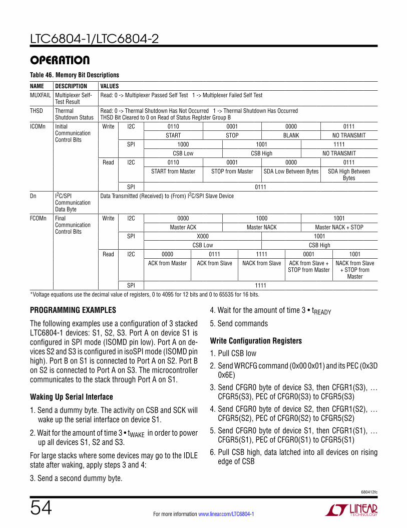
LTC6804-1/LTC6804-2
54680412fc
For more information www.linear.com/LTC6804-1
operaTion
NAME DESCRIPTION VALUESMUXFAIL Multiplexer Self-
Test ResultRead: 0 -> Multiplexer Passed Self Test 1 -> Multiplexer Failed Self Test
THSD Thermal Shutdown Status
Read: 0 -> Thermal Shutdown Has Not Occurred 1 -> Thermal Shutdown Has Occurred THSD Bit Cleared to 0 on Read of Status RegIster Group B
ICOMn Initial Communication Control Bits
Write I2C 0110 0001 0000 0111START STOP BLANK NO TRANSMIT
SPI 1000 1001 1111CSB Low CSB High NO TRANSMIT
Read I2C 0110 0001 0000 0111START from Master STOP from Master SDA Low Between Bytes SDA High Between
BytesSPI 0111
Dn I2C/SPI Communication Data Byte
Data Transmitted (Received) to (From) I2C/SPI Slave Device
FCOMn Final Communication Control Bits
Write I2C 0000 1000 1001Master ACK Master NACK Master NACK + STOP
SPI X000 1001CSB Low CSB High
Read I2C 0000 0111 1111 0001 1001ACK from Master ACK from Slave NACK from Slave ACK from Slave +
STOP from MasterNACK from Slave
+ STOP from Master
SPI 1111*Voltage equations use the decimal value of registers, 0 to 4095 for 12 bits and 0 to 65535 for 16 bits.
PROGRAMMING EXAMPLES
The following examples use a configuration of 3 stacked LTC6804-1 devices: S1, S2, S3. Port A on device S1 is configured in SPI mode (ISOMD pin low). Port A on de-vices S2 and S3 is configured in isoSPI mode (ISOMD pin high). Port B on S1 is connected to Port A on S2. Port B on S2 is connected to Port A on S3. The microcontroller communicates to the stack through Port A on S1.
Waking Up Serial Interface
1. Send a dummy byte. The activity on CSB and SCK will wake up the serial interface on device S1.
2. Wait for the amount of time 3 • tWAKE in order to power up all devices S1, S2 and S3.
For large stacks where some devices may go to the IDLE state after waking, apply steps 3 and 4:
3. Send a second dummy byte.
4. Wait for the amount of time 3 • tREADY
5. Send commands
Write Configuration Registers
1. Pull CSB low
2. Send WRCFG command (0x00 0x01) and its PEC (0x3D 0x6E)
3. Send CFGR0 byte of device S3, then CFGR1(S3), …CFGR5(S3), PEC of CFGR0(S3) to CFGR5(S3)
4. Send CFGR0 byte of device S2, then CFGR1(S2), …CFGR5(S2), PEC of CFGR0(S2) to CFGR5(S2)
5. Send CFGR0 byte of device S1, then CFGR1(S1), …CFGR5(S1), PEC of CFGR0(S1) to CFGR5(S1)
6. Pull CSB high, data latched into all devices on rising edge of CSB
Table 46. Memory Bit Descriptions
LTC6804-1/LTC6804-2
55680412fc
For more information www.linear.com/LTC6804-1
operaTionCalculation of serial interface time for sequence above:
Number of LTC6804-1s in daisy chain stack = nNumber of bytes in sequence (B):
Command: 2 (command byte) + 2 (command PEC) = 4
Data: 6 (Data bytes) + 2 (Data PEC) per LTC6804 = 8 bytes per device
B = 4 + 8 • nSerial port frequency per bit = F
Time = (1/F) • B • 8 bits/byte = (1/F) • [4 + 8 • n] • 8
Time for 3 LTC6804 example above, with 1MHz serial port = (1/1e6) • (4 + 8 • 3) • 8 = 224µs
Note: This time will remain the same for all write and read commands.
Read Cell Voltage Register Group A
1. Pull CSB low
2. Send RDCVA command (0x00 0x04) and its PEC (0x07 0xC2)
3. Read CVAR0 byte of device S1, then CVAR1(S1), … CVAR5(S1), PEC of CVAR0(S1) to CVAR5(S1)
4. Read CVAR0 byte of device S2, then CVAR1(S2), …CVAR5(S2), PEC of CVAR0(S2) to CVAR0(S2)
5. Read CVAR0 byte of device S3, then CVAR1(S3), … CVAR5(S3), PEC of CVAR0(S3) to CVAR5(S3)
6. Pull CSB high
Start Cell Voltage ADC Conversion
(All cells, normal mode with discharge permitted) and poll status
1. Pull CSB low
2. Send ADCV command with MD[1:0] = 10 and DCP = 1 i.e. 0x03 0x70 and its PEC (0xAF 0x42)
3. Pull CSB high
Clear Cell Voltage Registers
1. Pull CSB low
2. Send CLRCELL command (0x07 0x11) and its PEC (0xC9 0xC0)
3. Pull CSB high
Poll ADC Status
(Parallel configuration and ISOMD = 0)
This example uses an addressed LTC6804-2 with address A [3:0] = 0011 and ISOMD = 0
1. Pull CSB low
2. Send PLADC command (0x9F 0x14) and its PEC (0x1C 0x48 )
3. SDO output is pulled low if the LTC6804-2 is busy. The host needs to send clocks on SCK in order for the poll-ing status to be updated from the addressed device.
4. SDO output is high when the LTC6804-2 has completed conversions
5. Pull CSB high to exit polling
Talk to an I2C Slave Connected to LTC6804
The LTC6804 supports I2C slave devices by connection to GPIO4(SDA) and GPIO5(SCL). One valuable use for this capability is to store production calibration constants or other information in a small serial EEPROM using a con-nection like shown in Figure 25.
Figure 25. Connecting I2C EEPROM to LTC6804 GPIO Pins
680412 F25
GPIO5(SCL)
GPIO4(SDA)
4.7k
V–
VREG
LTC68041µF10V4.7k
WP
VCC24AA01
SCL
VSS
SDA
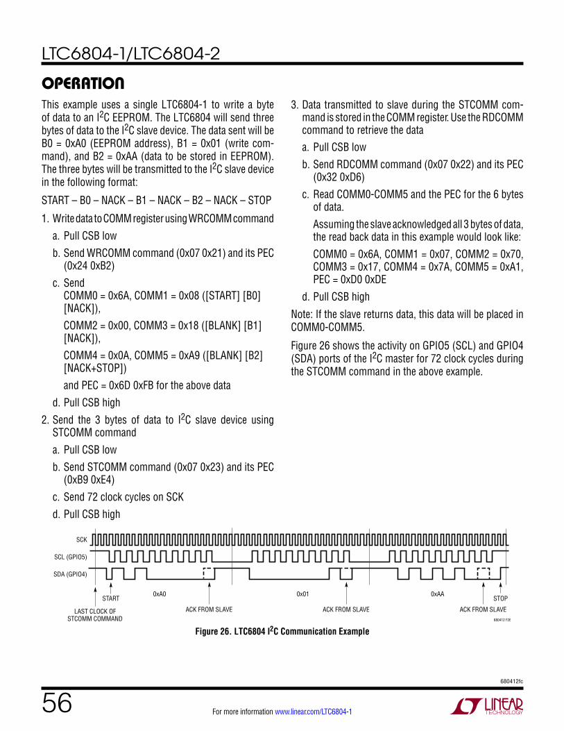
LTC6804-1/LTC6804-2
56680412fc
For more information www.linear.com/LTC6804-1
This example uses a single LTC6804-1 to write a byte of data to an I2C EEPROM. The LTC6804 will send three bytes of data to the I2C slave device. The data sent will be B0 = 0xA0 (EEPROM address), B1 = 0x01 (write com-mand), and B2 = 0xAA (data to be stored in EEPROM). The three bytes will be transmitted to the I2C slave device in the following format:
START – B0 – NACK – B1 – NACK – B2 – NACK – STOP
1. Write data to COMM register using WRCOMM command
a. Pull CSB low
b. Send WRCOMM command (0x07 0x21) and its PEC (0x24 0xB2)
c. Send COMM0 = 0x6A, COMM1 = 0x08 ([START] [B0] [NACK]),
COMM2 = 0x00, COMM3 = 0x18 ([BLANK] [B1] [NACK]),
COMM4 = 0x0A, COMM5 = 0xA9 ([BLANK] [B2] [NACK+STOP])
and PEC = 0x6D 0xFB for the above data
d. Pull CSB high
2. Send the 3 bytes of data to I2C slave device using STCOMM command
a. Pull CSB low
b. Send STCOMM command (0x07 0x23) and its PEC (0xB9 0xE4)
c. Send 72 clock cycles on SCK
d. Pull CSB high
3. Data transmitted to slave during the STCOMM com-mand is stored in the COMM register. Use the RDCOMM command to retrieve the dataa. Pull CSB low
b. Send RDCOMM command (0x07 0x22) and its PEC (0x32 0xD6)
c. Read COMM0-COMM5 and the PEC for the 6 bytes of data.
Assuming the slave acknowledged all 3 bytes of data, the read back data in this example would look like:
COMM0 = 0x6A, COMM1 = 0x07, COMM2 = 0x70, COMM3 = 0x17, COMM4 = 0x7A, COMM5 = 0xA1, PEC = 0xD0 0xDE
d. Pull CSB high
Note: If the slave returns data, this data will be placed in COMM0-COMM5.
Figure 26 shows the activity on GPIO5 (SCL) and GPIO4 (SDA) ports of the I2C master for 72 clock cycles during the STCOMM command in the above example.
Figure 26. LTC6804 I2C Communication Example680412 F26
SDA (GPIO4)
SCL (GPIO5)
START
ACK FROM SLAVE
0xA0 0x01 0xAA
SCK
STOP
LAST CLOCK OFSTCOMM COMMAND
ACK FROM SLAVE ACK FROM SLAVE
operaTion
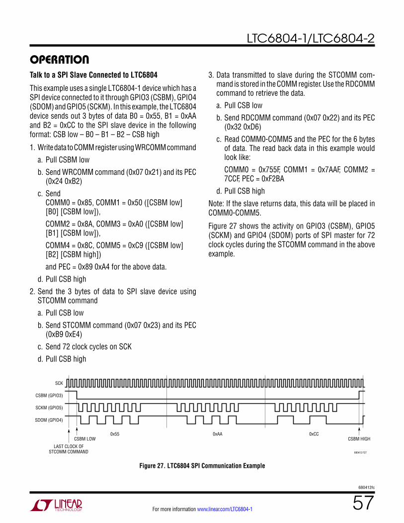
LTC6804-1/LTC6804-2
57680412fc
For more information www.linear.com/LTC6804-1
Talk to a SPI Slave Connected to LTC6804
This example uses a single LTC6804-1 device which has a SPI device connected to it through GPIO3 (CSBM), GPIO4 (SDOM) and GPIO5 (SCKM). In this example, the LTC6804 device sends out 3 bytes of data B0 = 0x55, B1 = 0xAA and B2 = 0xCC to the SPI slave device in the following format: CSB low – B0 – B1 – B2 – CSB high
1. Write data to COMM register using WRCOMM command
a. Pull CSBM low
b. Send WRCOMM command (0x07 0x21) and its PEC (0x24 0xB2)
c. Send COMM0 = 0x85, COMM1 = 0x50 ([CSBM low] [B0] [CSBM low]),
COMM2 = 0x8A, COMM3 = 0xA0 ([CSBM low] [B1] [CSBM low]),
COMM4 = 0x8C, COMM5 = 0xC9 ([CSBM low] [B2] [CSBM high])
and PEC = 0x89 0xA4 for the above data.
d. Pull CSB high
2. Send the 3 bytes of data to SPI slave device using STCOMM command
a. Pull CSB low
b. Send STCOMM command (0x07 0x23) and its PEC (0xB9 0xE4)
c. Send 72 clock cycles on SCK
d. Pull CSB high
3. Data transmitted to slave during the STCOMM com-mand is stored in the COMM register. Use the RDCOMM command to retrieve the data.
a. Pull CSB low
b. Send RDCOMM command (0x07 0x22) and its PEC (0x32 0xD6)
c. Read COMM0-COMM5 and the PEC for the 6 bytes of data. The read back data in this example would look like:
COMM0 = 0x755F, COMM1 = 0x7AAF, COMM2 = 7CCF, PEC = 0xF2BA
d. Pull CSB high
Note: If the slave returns data, this data will be placed in COMM0-COMM5.
Figure 27 shows the activity on GPIO3 (CSBM), GPIO5 (SCKM) and GPIO4 (SDOM) ports of SPI master for 72 clock cycles during the STCOMM command in the above example.
operaTion
Figure 27. LTC6804 SPI Communication Example
680412 F27
SDOM (GPIO4)
SCKM (GPIO5)
CSBM LOW0x55 0xAA 0xCC
CSBM (GPIO3)
SCK
CSBM HIGH
LAST CLOCK OFSTCOMM COMMAND
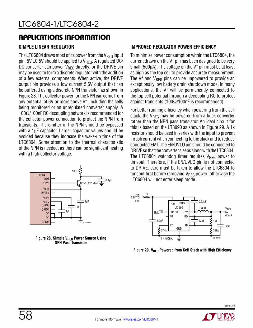
LTC6804-1/LTC6804-2
58680412fc
For more information www.linear.com/LTC6804-1
applicaTions inForMaTionSIMPLE LINEAR REGULATOR
The LTC6804 draws most of its power from the VREG input pin. 5V ±0.5V should be applied to VREG. A regulated DC/DC converter can power VREG directly, or the DRIVE pin may be used to form a discrete regulator with the addition of a few external components. When active, the DRIVE output pin provides a low current 5.6V output that can be buffered using a discrete NPN transistor, as shown in Figure 28. The collector power for the NPN can come from any potential of 6V or more above V–, including the cells being monitored or an unregulated converter supply. A 100Ω/100nF RC decoupling network is recommended for the collector power connection to protect the NPN from transients. The emitter of the NPN should be bypassed with a 1µF capacitor. Larger capacitor values should be avoided because they increase the wake-up time of the LTC6804. Some attention to the thermal characteristic of the NPN is needed, as there can be significant heating with a high collector voltage.
Figure 28. Simple VREG Power Source Using NPN Pass Transistor
VIN BOOSTLT3990
SWEN/UVLOPG
RT
0.22µF
22pF
374k
f = 400kHz
22µF
2.2µF
VIN28V TO
62V
VREG5V40mA
1M
316k
1k
33µH
BD
FBGND
OFF ON
680412 F29
1µF
0.1µF
100Ω
680412 F28
WDTDRIVE
VREGSWTEN
VREF1VREF2GPIO5GPIO4
V–
V–
GPIO3
1µF
1µF
LTC6804
NSV1C201MZ4
IMPROVED REGULATOR POWER EFFICIENCY
To minimize power consumption within the LTC6804, the current drawn on the V+ pin has been designed to be very small (500µA). The voltage on the V+ pin must be at least as high as the top cell to provide accurate measurement. The V+ and VREG pins can be unpowered to provide an exceptionally low battery drain shutdown mode. In many applications, the V+ will be permanently connected to the top cell potential through a decoupling RC to protect against transients (100Ω/100nF is recommended).
For better running efficiency when powering from the cell stack, the VREG may be powered from a buck converter rather than the NPN pass transistor. An ideal circuit for this is based on the LT3990 as shown in Figure 29. A 1k resistor should be used in series with the input to prevent inrush current when connecting to the stack and to reduce conducted EMI. The EN/UVLO pin should be connected to DRIVE so that the converter sleeps along with the LTC6804. The LTC6804 watchdog timer requires VREG power to timeout. Therefore, if the EN/UVLO pin is not connected to DRIVE, care must be taken to allow the LTC6804 to timeout first before removing VREG power; otherwise the LTC6804 will not enter sleep mode.
Figure 29. VREG Powered from Cell Stack with High Efficiency
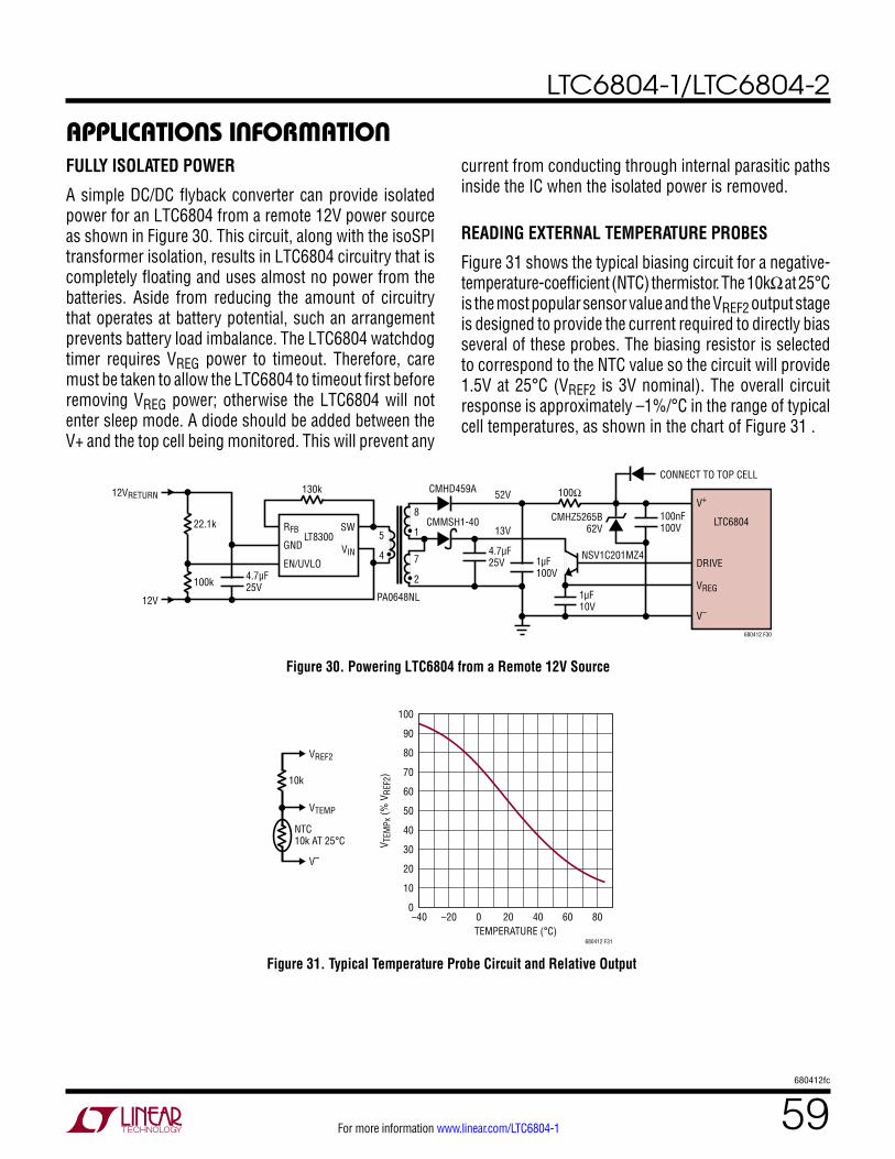
LTC6804-1/LTC6804-2
59680412fc
For more information www.linear.com/LTC6804-1
applicaTions inForMaTionFULLY ISOLATED POWER
A simple DC/DC flyback converter can provide isolated power for an LTC6804 from a remote 12V power source as shown in Figure 30. This circuit, along with the isoSPI transformer isolation, results in LTC6804 circuitry that is completely floating and uses almost no power from the batteries. Aside from reducing the amount of circuitry that operates at battery potential, such an arrangement prevents battery load imbalance. The LTC6804 watchdog timer requires VREG power to timeout. Therefore, care must be taken to allow the LTC6804 to timeout first before removing VREG power; otherwise the LTC6804 will not enter sleep mode. A diode should be added between the V+ and the top cell being monitored. This will prevent any
Figure 30. Powering LTC6804 from a Remote 12V Source
TEMPERATURE (°C)–40 0
V TEM
Px (%
VRE
F2)
100
80
60
40
20
90
70
50
30
10
0–20 20 6040 80
680412 F31
10k
NTC10k AT 25°C
V–
VREF2
VTEMP
680412 F30
DRIVE
VREG
V–
V+
LTC6804100nF100V
CMHZ5265B62V
NSV1C201MZ4
CMHD459A
PA0648NL
CMMSH1-40
GND
EN/UVLO
RFBLT8300
130k 100Ω
SW
VIN
1µF10V
4.7µF25V7
2
8
15
4 1µF100V
22.1k
100k
12V
52V
13V
12VRETURN
4.7µF25V
•
•
•
CONNECT TO TOP CELL
current from conducting through internal parasitic paths inside the IC when the isolated power is removed.
READING EXTERNAL TEMPERATURE PROBES
Figure 31 shows the typical biasing circuit for a negative-temperature-coefficient (NTC) thermistor. The 10kΩ at 25°C is the most popular sensor value and the VREF2 output stage is designed to provide the current required to directly bias several of these probes. The biasing resistor is selected to correspond to the NTC value so the circuit will provide 1.5V at 25°C (VREF2 is 3V nominal). The overall circuit response is approximately –1%/°C in the range of typical cell temperatures, as shown in the chart of Figure 31 .
Figure 31. Typical Temperature Probe Circuit and Relative Output
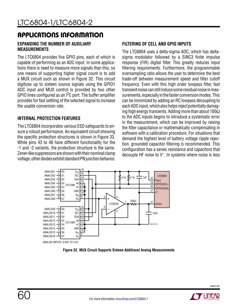
LTC6804-1/LTC6804-2
60680412fc
For more information www.linear.com/LTC6804-1
S0S1S2S3S4S5S6S7
VCCSCLSDA
A0A1
GNDVEEDO
ANALOG1ANALOG2ANALOG3ANALOG4ANALOG5ANALOG6ANALOG7ANALOG8
12345678
161514131211109
LTC1380
S0S1S2S3S4S5S6S7
VCCSCLSDA
A0A1
GNDVEEDO
ANALOG9ANALOG10ANALOG11ANALOG12ANALOG13ANALOG14ANALOG15ANALOG16
12345678
161514131211109
LTC1380
3
27
31
3233
37
5
1µF
10nF
680412 F32
VREGGPIO5(SCL)GPIO4(SDA)V–
GPIO1
LTC68044.7k4.7k
1
24
–
+LTC6255
100Ω
ANALOG INPUTS: 0.04V TO 4.5V
applicaTions inForMaTionEXPANDING THE NUMBER OF AUXILIARY MEASUREMENTS
The LTC6804 provides five GPIO pins, each of which is capable of performing as an ADC input. In some applica-tions there is need to measure more signals than this, so one means of supporting higher signal count is to add a MUX circuit such as shown in Figure 32. This circuit digitizes up to sixteen source signals using the GPIO1 ADC input and MUX control is provided by two other GPIO lines configured as an I2C port. The buffer amplifier provides for fast settling of the selected signal to increase the usable conversion rate.
INTERNAL PROTECTION FEATURES
The LTC6804 incorporates various ESD safeguards to en-sure a robust performance. An equivalent circuit showing the specific protection structures is shown in Figure 33. While pins 43 to 48 have different functionality for the -1 and -2 variants, the protection structure is the same. Zener-like suppressors are shown with their nominal clamp voltage, other diodes exhibit standard PN junction behavior.
Figure 32. MUX Circuit Supports Sixteen Additional Analog Measurements
Figure 33. Internal ESD Protection Structure of LTC6804
FILTERING OF CELL AND GPIO INPUTS
The LTC6804 uses a delta-sigma ADC, which has delta-sigma modulator followed by a SINC3 finite impulse response (FIR) digital filter. This greatly reduces input filtering requirements. Furthermore, the programmable oversampling ratio allows the user to determine the best trade-off between measurement speed and filter cutoff frequency. Even with this high order lowpass filter, fast transient noise can still induce some residual noise in mea-surements, especially in the faster conversion modes. This can be minimized by adding an RC lowpass decoupling to each ADC input, which also helps reject potentially damag-ing high energy transients. Adding more than about 100Ω to the ADC inputs begins to introduce a systematic error in the measurement, which can be improved by raising the filter capacitance or mathematically compensating in software with a calibration procedure. For situations that demand the highest level of battery voltage ripple rejec-tion, grounded capacitor filtering is recommended. This configuration has a series resistance and capacitors that decouple HF noise to V–. In systems where noise is less
LTC6804-1/LTC6804-2
61680412fc
For more information www.linear.com/LTC6804-1
EXPANDING THE NUMBER OF AUXILIARY MEASUREMENTS
The LTC6804 provides five GPIO pins, each of which is capable of performing as an ADC input. In some applica-tions there is need to measure more signals than this, so one means of supporting higher signal count is to add a MUX circuit such as shown in Figure 32. This circuit digitizes up to sixteen source signals using the GPIO1 ADC input and MUX control is provided by two other GPIO lines configured as an I2C port. The buffer amplifier provides for fast settling of the selected signal to increase the usable conversion rate.
INTERNAL PROTECTION FEATURES
The LTC6804 incorporates various ESD safeguards to en-sure a robust performance. An equivalent circuit showing the specific protection structures is shown in Figure 33. While pins 43 to 48 have different functionality for the -1 and -2 variants, the protection structure is the same. Zener-like suppressors are shown with their nominal clamp voltage, other diodes exhibit standard PN junction behavior.
Figure 32. MUX Circuit Supports Sixteen Additional Analog Measurements
Figure 33. Internal ESD Protection Structure of LTC6804
applicaTions inForMaTionperiodic or higher oversample rates are in use, a differential capacitor filter structure is adequate. In this configuration there are series resistors to each input, but the capacitors connect between the adjacent C pins. However, the dif-ferential capacitor sections interact. As a result, the filter response is less consistent and results in less attenuation than predicted by the RC, by approximately a decade. Note that the capacitors only see one cell of applied voltage (thus smaller and lower cost) and tend to distribute transient energy uniformly across the IC (reducing stress events on the internal protection structure). Figure 34 shows the two methods schematically. Basic ADC accuracy varies with R, C as shown in the Typical Performance curves, but error is minimized if R = 100Ω and C = 10nF. The GPIO pins will always use a grounded capacitor configuration because the measurements are all with respect to V–.
Figure 34. Input Filter Structure Configurations680412 F33
LTC6804
10k
12V
C12
S12
12V
10k
12V
C11
S11
12V
10k
12V
C10
S10
12V
10k
12V
C9
S9
12V
10k
12V
C8
S8
12V
10k
12V
C7
S7
12V
10k
12V
C6
S6
12V
10k
12V
C5
S5
12V
10k
12V
C4
S4
12V
10k
12V
C3
S3
12V
10k
12V
C2
S2
12V
10k
12V
25Ω
C1
S1
12VC0
V–
V–
30V
30V
30V
30V
30V
30V
GPIO112V
GPIO212V
GPIO312V
GPIO4
GPIO5
12V
VREF212V
12V
VREF112V
SWTEN12V
VREG12V
DRIVE12V
WDT12V
ISOMD12V
CSB12V
SCK12V
SDI12V
SDO12V
IBIAS/A012V
ICMP/A112V
IMB/A212V
IPB/A312V
V+
NOTE: NOT SHOWN ARE PN DIODES TO ALL OTHER PINS FROM PIN 31
48
47
46
45
44
43
42
41
40
39
38
37
36
35
34
32
33
31
30
29
28
27
25
26
12
3
4
5
6
7
8
9
10
11
12
13
14
15
16
17
18
19
20
21
22
23
24
680412 F34
CELL2
V–
C2
10nF
BATTERY V–
100Ω
Differential Capacitor Filter
BSS308PE
33Ω
3.3k
CELL1 C1
S2
S1
LTC6804
LTC6804
S2
S1
10nF
10nF
100Ω
BSS308PE
33Ω
100ΩC0
3.3k
CELL2
V–
C2
BATTERY V–
100Ω
Grounded Capacitor Filter
BSS308PE
33Ω
3.3k
*
CELL1 C1100Ω
BSS308PE
*6.8V ZENERS RECOMMENDED IF C > 100nF
33Ω
C0
C
C
C
3.3k
*
*
100Ω
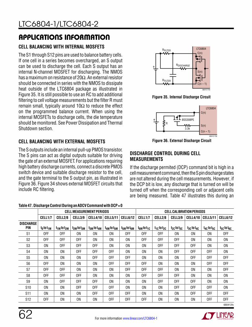
LTC6804-1/LTC6804-2
62680412fc
For more information www.linear.com/LTC6804-1
applicaTions inForMaTionCELL BALANCING WITH INTERNAL MOSFETS
The S1 through S12 pins are used to balance battery cells. If one cell in a series becomes overcharged, an S output can be used to discharge the cell. Each S output has an internal N-channel MOSFET for discharging. The NMOS has a maximum on resistance of 20Ω. An external resistor should be connected in series with the NMOS to dissipate heat outside of the LTC6804 package as illustrated in Figure 35. It is still possible to use an RC to add additional filtering to cell voltage measurements but the filter R must remain small, typically around 10Ω to reduce the effect on the programmed balance current. When using the internal MOSFETs to discharge cells, the die temperature should be monitored. See Power Dissipation and Thermal Shutdown section.
CELL BALANCING WITH EXTERNAL MOSFETS
The S outputs include an internal pull-up PMOS transistor. The S pins can act as digital outputs suitable for driving the gate of an external MOSFET. For applications requiring high battery discharge currents, connect a discrete PMOS switch device and suitable discharge resistor to the cell, and the gate terminal to the S output pin, as illustrated in Figure 36. Figure 34 shows external MOSFET circuits that include RC filtering.
Figure 35. Internal Discharge Circuit
Figure 36. External Discharge Circuit
Table 47. Discharge Control During an ADCV Command with DCP = 0CELL MEASUREMENT PERIODS CELL CALIBRATION PERIODS
CELL1/7 CELL2/8 CELL3/9 CELL4/10 CELL5/11 CELL6/12 CELL1/7 CELL2/8 CELL3/9 CELL4/10 CELL5/11 CELL6/12
DISCHARGE PIN t0 to t1M t1M to t2M t2M to t3M t3M to t4M t4M to t5M t5M to t6M t6M to t1C t1C to t2C t2C to t3C t3C to t4C t4C to t5C t5C to t6C
S1 OFF OFF ON ON ON OFF OFF OFF ON ON ON OFF
S2 OFF OFF OFF ON ON ON OFF OFF OFF ON ON ON
S3 ON OFF OFF OFF ON ON ON OFF OFF OFF ON ON
S4 ON ON OFF OFF OFF ON ON ON OFF OFF OFF ON
S5 ON ON ON OFF OFF OFF ON ON ON OFF OFF OFF
S6 OFF ON ON ON OFF OFF OFF ON ON ON OFF OFF
S7 OFF OFF ON ON ON OFF OFF OFF ON ON ON OFF
S8 OFF OFF OFF ON ON ON OFF OFF OFF ON ON ON
S9 ON OFF OFF OFF ON ON ON OFF OFF OFF ON ON
S10 ON ON OFF OFF OFF ON ON ON OFF OFF OFF ON
S11 ON ON ON OFF OFF OFF ON ON ON OFF OFF OFF
S12 OFF ON ON ON OFF OFF OFF ON ON ON OFF OFF
LTC6804
680412 F35
RFILTER
RFILTER
RDISCHARGE
C(n)
S(n)
C(n – 1)
+
LTC6804
680412 F36
RBSS308PE
3.3k
C(n)
S(n)
C(n – 1)
+
DISCHARGE CONTROL DURING CELL MEASUREMENTS
If the discharge permited (DCP) command bit is high in a cell measurement command, then the S pin discharge states are not altered during the cell measurements. However, if the DCP bit is low, any discharge that is turned on will be turned off when the corresponding cell or adjacent cells are being measured. Table 47 illustrates this during an
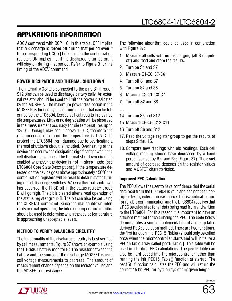
LTC6804-1/LTC6804-2
63680412fc
For more information www.linear.com/LTC6804-1
applicaTions inForMaTionADCV command with DCP = 0. In this table, OFF implies that a discharge is forced off during that period even if the corresponding DCC[x] bit is high in the configuration register. ON implies that if the discharge is turned on, it will stay on during that period. Refer to Figure 3 for the timing of the ADCV command.
POWER DISSIPATION AND THERMAL SHUTDOWN
The internal MOSFETs connected to the pins S1 through S12 pins can be used to discharge battery cells. An exter-nal resistor should be used to limit the power dissipated by the MOSFETs. The maximum power dissipation in the MOSFETs is limited by the amount of heat that can be tol-erated by the LTC6804. Excessive heat results in elevated die temperatures. Little or no degradation will be observed in the measurement accuracy for die temperatures up to 125°C. Damage may occur above 150°C, therefore the recommended maximum die temperature is 125°C. To protect the LTC6804 from damage due to overheating a thermal shutdown circuit is included. Overheating of the device can occur when dissipating significant power in the cell discharge switches. The thermal shutdown circuit is enabled whenever the device is not in sleep mode (see LTC6804 Core State Descriptions). If the temperature de-tected on the device goes above approximately 150°C the configuration registers will be reset to default states turn-ing off all discharge switches. When a thermal shutdown has occurred, the THSD bit in the status register group B will go high. The bit is cleared after a read operation of the status register group B. The bit can also be set using the CLRSTAT command. Since thermal shutdown inter-rupts normal operation, the internal temperature monitor should be used to determine when the device temperature is approaching unacceptable levels.
METHOD TO VERIFY BALANCING CIRCUITRY
The functionality of the discharge circuitry is best verified by cell measurements. Figure 37 shows an example using the LTC6804 battery monitor IC. The resistor between the battery and the source of the discharge MOSFET causes cell voltage measurements to decrease. The amount of measurement change depends on the resistor values and the MOSFET on resistance.
The following algorithm could be used in conjunction with Figure 37:
1. Measure all cells with no discharging (all S outputs off) and read and store the results.
2. Turn on S1 and S73. Measure C1-C0, C7-C64. Turn off S1 and S75. Turn on S2 and S86. Measure C2-C1, C8-C7
7. Turn off S2 and S8
…14. Turn on S6 and S1215. Measure C6-C5, C12-C1116. Turn off S6 and S1217. Read the voltage register group to get the results of
steps 2 thru 16.
18. Compare new readings with old readings. Each cell voltage reading should have decreased by a fixed percentage set by RB1 and RB2 (Figure 37). The exact amount of decrease depends on the resistor values and MOSFET characteristics.
Improved PEC Calculation
The PEC allows the user to have confidence that the serial data read from the LTC6804 is valid and has not been cor-rupted by any external noise source. This is a critical feature for reliable communication and the LTC6804 requires that a PEC be calculated for all data being read from and written to the LTC6804. For this reason it is important to have an efficient method for calculating the PEC. The code below demonstrates a simple implementation of a lookup table derived PEC calculation method. There are two functions, the first function init_PEC15_Table() should only be called once when the microcontroller starts and will initialize a PEC15 table array called pec15Table[]. This table will be used in all future PEC calculations. The pec15 table can also be hard coded into the microcontroller rather than running the init_PEC15_Table() function at startup. The pec15() function calculates the PEC and will return the correct 15 bit PEC for byte arrays of any given length.
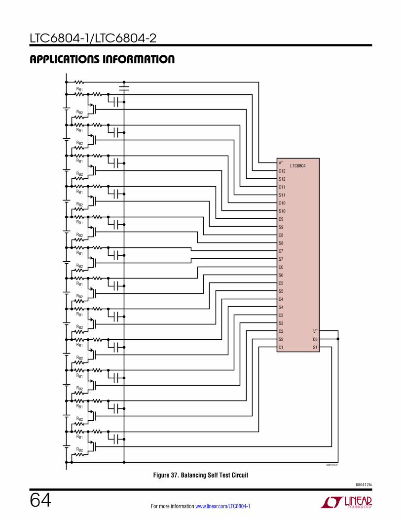
LTC6804-1/LTC6804-2
64680412fc
For more information www.linear.com/LTC6804-1
applicaTions inForMaTion
Figure 37. Balancing Self Test Circuit
680412 F37
V+
C12
S12
C11
S11
C10
S10
C9
S9
C8
S8
C7
S7
C6
S6
C5
S5
C4
S4
C3
S3
C2
S2
C1
V–
C0
S1
LTC6804
RB1
RB1
RB2
RB1
RB2
RB1
RB2
RB1
RB2
RB1
RB2
RB1
RB2
RB1
RB2
RB1
RB2
RB1
RB2
RB1
RB2
RB1
RB2
RB2
LTC6804-1/LTC6804-2
65680412fc
For more information www.linear.com/LTC6804-1
applicaTions inForMaTion/************************************
Copyright 2012 Linear Technology Corp. (LTC)Permission to freely use, copy, modify, and distribute this software for any purpose with or without fee is hereby granted, provided that the above copyright notice and this permission notice appear in all copies:
THIS SOFTWARE IS PROVIDED “AS IS” AND LTC DISCLAIMS ALL WARRANTIESINCLUDING ALL IMPLIED WARRANTIES OF MERCHANTABILITY AND FITNESS. IN NOEVENT SHALL LTC BE LIABLE FOR ANY SPECIAL, DIRECT, INDIRECT, OR CONSEQUENTIALDAMAGES OR ANY DAMAGES WHATSOEVER RESULTING FROM ANY USE OF SAME, INCLUDINGANY LOSS OF USE OR DATA OR PROFITS, WHETHER IN AN ACTION OF CONTRACT, NEGLIGENCEOR OTHER TORTUOUS ACTION, ARISING OUT OF OR IN CONNECTION WITH THE USE OR PERFORMANCE OF THIS SOFTWARE.
***********************************************************/
int16 pec15Table[256];int16 CRC15_POLY = 0x4599;void init_PEC15_Table(){ for (int i = 0; i < 256; i++) { remainder = i << 7; for (int bit = 8; bit > 0; --bit) { if (remainder & 0x4000) { remainder = ((remainder << 1)); remainder = (remainder ^ CRC15poly) } else { remainder = ((remainder << 1)); } } pec15Table[i] = remainder&0xFFFF; }}
unsigned int16 pec15 (char *data , int len){ int16 remainder,address; remainder = 16;//PEC seed for (int i = 0; i < len; i++) { address = ((remainder >> 7) ^ data[i]) & 0xff;//calculate PEC table address remainder = (remainder << 8 ) ^ pec15Table[address]; } return (remainder*2);//The CRC15 has a 0 in the LSB so the final value must be multiplied by 2}
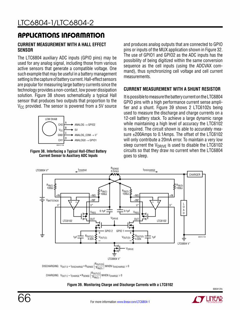
LTC6804-1/LTC6804-2
66680412fc
For more information www.linear.com/LTC6804-1
applicaTions inForMaTionCURRENT MEASUREMENT WITH A HALL EFFECT SENSOR
The LTC6804 auxiliary ADC inputs (GPIO pins) may be used for any analog signal, including those from various active sensors that generate a compatible voltage. One such example that may be useful in a battery management setting is the capture of battery current. Hall-effect sensors are popular for measuring large battery currents since the technology provides a non-contact, low power dissipation solution. Figure 38 shows schematically a typical Hall sensor that produces two outputs that proportion to the VCC provided. The sensor is powered from a 5V source
Figure 38. Interfacing a Typical Hall-Effect Battery Current Sensor to Auxiliary ADC Inputs
and produces analog outputs that are connected to GPIO pins or inputs of the MUX application shown in Figure 32. The use of GPIO1 and GPIO2 as the ADC inputs has the possibility of being digitized within the same conversion sequence as the cell inputs (using the ADCVAX com-mand), thus synchronizing cell voltage and cell current measurements.
CURRENT MEASUREMENT WITH A SHUNT RESISTOR
It is possible to measure the battery current on the LTC6804 GPIO pins with a high performance current sense ampli-fier and a shunt. Figure 39 shows 2 LTC6102s being used to measure the discharge and charge currents on a 12-cell battery stack. To achieve a large dynamic range while maintaining a high level of accuracy the LTC6102 is required. The circuit shown is able to accurately mea-sure ±200Amps to 0.1Amps. The offset of the LTC6102 will only contribute a 20mA error. To maintain a very low sleep current the VDRIVE is used to disable the LTC6102 circuits so that they draw no current when the LTC6804 goes to sleep.
CHARGER
–+ – +
+
–
+
–
LOAD
VOUT D = IDISCHARGE • RSENSE ( ) WHEN IDISCHARGE ≥ 0DISCHARGING:ROUT(D)RIN(D)
VOUT C = ICHARGE • RSENSE ( ) WHEN ICHARGE ≥ 0CHARGING:ROUT(C)RIN(C)
680412 F39
VBATTSTACK
RIN(D)100Ω
LTC6102
LTC6804 V–
LTC6804 V–
VDRIVE
VDRIVE
RIN(C)100Ω
RIN(D)100Ω
LTC6102
LTC6804 V+
VOUT(C)ROUT(C)
4.02kROUT(D)4.02k
VOUT(D)
GPIO 1GPIO 2
RIN(C)100Ω
ICHARGERSENSE0.5mΩ IDISCHARGE
V+V–
OUT
–INS+IN
V+ V–
OUT
–INS +IN
–INF –INF
VREG0.1µF VREG
0.1µF
1µF1µF
Figure 39. Monitoring Charge and Discharge Currents with a LTC6102
680412 F38
LEM DHAB
CH2 ANALOG → GPIO2
VCC 5V
GND ANALOG_COM → V–
CH1 ANALOG0 → GPIO1
A
B
C
D
LTC6804-1/LTC6804-2
67680412fc
For more information www.linear.com/LTC6804-1
applicaTions inForMaTionUSING THE LTC6804 WITH LESS THAN 12 CELLS
If the LTC6804 is powered by the battery stack, the minimum number of cells that can be monitored by the LTC6804 is governed by the supply voltage requirements of the LTC6804. V+ must be at least 11V to properly bias the LTC6804. Figure 40 shows an example of the LTC6804 when used to monitor eight cells with best cell measurement synchronization. The 12 cells monitored by the LTC6804 are split into two groups of 6 cells and are measured using two internal multiplexers and two ADCs. To optimize measurement synchronization in applications with less than 12 Cells the unused C pins should be equally distributed between the top of the second mux (C12) and the top of the first mux (C6). If there are an odd number of cells being used, the top mux should have fewer cells connected. The unused cell channels should be tied to the other unused channels on the same mux and then connected to the battery stack through a 100Ω resistor. The unused inputs will result in a reading of 0V for those cells channels. It is also acceptable to connect in the con-ventional sequence with all unused cell inputs at the top.
isoSPI IBIAS and ICMP Setup
The LTC6804 allows the isoSPI links of each application to be optimized for power consumption or for noise immunity. The power and noise immunity of an isoSPI system is determined by the programmed IB current, which controls the isoSPI signaling currents. Bias current IB can range from 100μA to 1mA. Internal circuitry scales up this bias current to create the isoSPI signal currents equal to 20 • IB. A low IB reduces the isoSPI power consumption in the READY and ACTIVE states, while a high IB increases the amplitude of the differential signal voltage VA across the matching termination resistor, RM. The IB current is programmed by the sum of the RB1 and RB2 resistors connected between the 2V IBIAS pin and GND as shown in
Figure 40. 8 Cell Connection Scheme
680412 F40
V+
C12
S12
C11
S11
C10
S10
C9
S9
C8
S8
C7
S7
C6
S6
C5
S5
C4
S4
C3
S3
C2
S2
C1
S1
C0
V–
LTC6804
+
+
+
+
+
+
+
+
NEXT HIGHER GROUPOF 8 CELLS
NEXT LOWER GROUPOF 8 CELLS
Figure 41. The receiver input threshold is set by the ICMP voltage that is programmed with the resistor divider created by the RB1 and RB2 resistors. The receiver threshold will be half of the voltage present on the ICMP pin.
LTC6804-1/LTC6804-2
68680412fc
For more information www.linear.com/LTC6804-1
applicaTions inForMaTion
The following guidelines should be used when setting the bias current (100µA to 1mA) IB and the receiver compara-tor threshold voltage VICMP/2:
RM = Transmission Line Characteristic Impedance Z0
Signal Amplitude VA = (20 • IB) • (RM/2)
VTCMP (Receiver Comparator Threshold) = K • VA
VICMP (voltage on ICMP pin) = 2 • VTCMP
RB2 = VICMP/IB RB1 = (2/IB) – RB2
Select IB and K (Signal Amplitude VA to Receiver Compara-tor Threshold ratio) according to the application:
For lower power links: IB = 0.5mA and K = 0.5
For full power links: IB = 1mA and K = 0.5
For long links (>50m): IB = 1mA and K = 0.25
For addressable multi-drop: IB = 1mA and K = 0.4
For applications with little system noise, setting IB to 0.5mA is a good compromise between power consumption and noise immunity. Using this IB setting with a 1:1 transformer and RM = 100Ω, RB1 should be set to 3.01k and RB2 set to 1k. With typical CAT5 twisted pair, these settings will allow for communication up to 50m. For applications in very noisy environments or that require cables longer than 50m it is recommended to increase IB to 1mA. Higher drive current compensates for the increased insertion loss in the cable and provides high noise immunity. When using cables over 50m and a transformer with a 1:1 turns ratio and RM = 100Ω, RB1 would be 1.5k and RB2 would be 499Ω.
RM
IPA ISOMD VREG
IMA
+
–
+
–
IBIAS
ICMP
680412 F41
LTC6804RM
RB1
RB2
RB1
RB2
IPBISOMD
IMB
IBIAS
ICMP
MOSIMISOSCKCS
SDOSDISCKCS
LTC6804
TWISTED-PAIR CABLEWITH CHARACTERISTIC IMPEDANCE RM
ISOLATION BARRIER(MAY USE ONE OR TWO TRANFORMERS)
MASTER•• ••
2V
VA
2V
VA
Figure 41. isoSPI Circuit
The maximum clock rate of an isoSPI link is determined by the length of the isoSPI cable. For cables 10 meters or less, the maximum 1MHz SPI clock frequency is pos-sible. As the length of the cable increases, the maximum possible SPI clock rate decreases. This dependence is a result of the increased propagation delays that can cre-ate possible timing violations. Figure 42 shows how the maximum data rate reduces as the cable length increases when using a CAT5 twisted pair.
Cable delay affects three timing specifications: tCLK, t6 and t7. In the Electrical Characteristics table, each of these specifications is de-rated by 100ns to allow for 50ns of cable delay. For longer cables, the minimum timing pa-rameters may be calculated as shown below:
tCLK, t6 and t7 > 0.9μs + 2 • tCABLE(0.2m per ns)
CABLE LENGTH (METERS)1
DATA
RAT
E (M
bps)
1.2
0.8
0.4
0.2
1.0
0.6
010
680412 F42
100
CAT5 ASSUMED
Figure 42. Data Rate vs Cable Length
LTC6804-1/LTC6804-2
69680412fc
For more information www.linear.com/LTC6804-1
applicaTions inForMaTionImplementing a Modular isoSPI Daisy Chain
The hardware design of a daisy-chain isoSPI bus is identi-cal for each device in the network due to the daisy-chain point-to-point architecture. The simple design as shown in Figure 41 is functional, but inadequate for most designs. The termination resistor RM should be split and bypassed with a capacitor as shown in Figure 43. This change provides both a differential and a common mode termination, and as such, increases the system noise immunity.
The use of cables between battery modules, particularly in automotive applications, can lead to increased noise susceptibility in the communication lines. For high levels of electromagnetic interference (EMC), additional filtering is recommended. The circuit example in Figure 43 shows the use of common mode chokes (CMC)to add common mode noise rejection from transients on the battery lines. The use of a center tapped transformer will also provide additional noise performance. A bypass capacitor con-nected to the center tap creates a low impedance for common mode noise (Figure 43b). Since transformers without a center tap can be less expensive, they may be preferred. In this case, the addition of a split termination resistor and a bypass capacitor (Figure 43a) can enhance the isoSPI performance. Large center tap capacitors greater than 10nF should be avoided as they may prevent the isoSPI common mode voltage from settling. Common mode chokes similar to those used in Ethernet or CANbus applications are recommended. Specific examples are provided in Table 49.
isoSPI LINK
XFMR
isoSPI LINK
CT XFMR
LTC6804-1
LTC6804-1
IP
IM
V–
10nF
100µH CMC
10nF
•
•62Ω
62Ω
300Ω
300Ω
••
a)
IP
IM
V–
10nF
100µH CMC
10nF
•
•51Ω
51Ω
••
b)
680412 F43
Figure 43. Daisy Chain Interface Components
An important daisy chain design consideration is the number of devices in the isoSPI network. The length of the chain determines the serial timing and affects data latency and throughput. The maximum number of devices in an isoSPI daisy chain is strictly dictated by the serial timing requirements. However, it is important to note that the serial read back time, and the increased current consumption, might dictate a practical limitation.
For a daisy chain, two timing considerations for proper operation dominate (see Figure 20):
1. t6, the time between the last clock and the rising chip select, must be long enough.
2. t5, the time from a rising chip select to the next falling chip select (between commands), must be long enough.
Both t5 and t6 must be lengthened as the number of LTC6804 devices in the daisy chain increases. The equa-tions for these times are below:
t5 > (#devices • 70ns) + 900ns
t6 > (#devices • 70ns) + 950ns
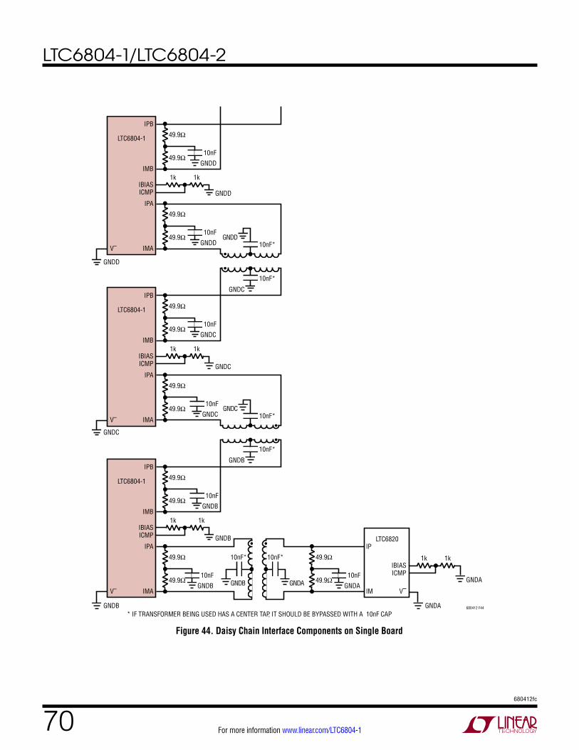
LTC6804-1/LTC6804-2
70680412fc
For more information www.linear.com/LTC6804-1
10nF
GNDD
10nF
GNDD
GNDD
GNDD
10nF
GNDC
10nF
GNDC
GNDC
GNDC
10nF
GNDB
10nF
GNDB
GNDB
10nF
GNDA
GNDB
GNDA
10nF*10nF*
1k 1k
••
GNDC
1k 1k
•
•
GNDB
1k 1k
1k 1k
••
GNDA
GNDD
GNDB GNDA
10nF*
GNDC10nF*
10nF*
10nF*
49.9Ω
49.9Ω
IPA
IBIASICMP
LTC6804-1
IMA
49.9Ω
49.9Ω
IPB
IMB
49.9Ω
49.9Ω
IPA
IBIASICMP
LTC6804-1
IMA
49.9Ω
49.9Ω
IPB
IMB
49.9Ω
49.9Ω
IPA
IBIASICMP
IBIASICMP
LTC6804-1
V–
V–
V–
IMA
49.9Ω
49.9Ω
IP
IM V–
49.9Ω
49.9Ω
IPB
IMB
* IF TRANSFORMER BEING USED HAS A CENTER TAP, IT SHOULD BE BYPASSED WITH A 10nF CAP680412 F44
LTC6820
Figure 44. Daisy Chain Interface Components on Single Board
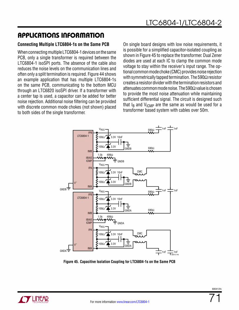
LTC6804-1/LTC6804-2
71680412fc
For more information www.linear.com/LTC6804-1
applicaTions inForMaTionConnecting Multiple LTC6804-1s on the Same PCB
When connecting multiple LTC6804-1 devices on the same PCB, only a single transformer is required between the LTC6804-1 isoSPI ports. The absence of the cable also reduces the noise levels on the communication lines and often only a split termination is required. Figure 44 shows an example application that has multiple LTC6804-1s on the same PCB, communicating to the bottom MCU through an LTC6820 isoSPI driver. If a transformer with a center tap is used, a capacitor can be added for better noise rejection. Additional noise filtering can be provided with discrete common mode chokes (not shown) placed to both sides of the single transformer.
On single board designs with low noise requirements, it is possible for a simplified capacitor-isolated coupling as shown in Figure 45 to replace the transformer. Dual Zener diodes are used at each IC to clamp the common mode voltage to stay within the receiver’s input range. The op-tional common mode choke (CMC) provides noise rejection with symmetrically tapped termination. The 590Ω resistor creates a resistor divider with the termination resistors and attenuates common mode noise. The 590Ω value is chosen to provide the most noise attenuation while maintaining sufficient differential signal. The circuit is designed such that IB and VICMP are the same as would be used for a transformer based system with cables over 50m.
10nF
GNDB
GNDB
GNDB
VREG
10nF
GNDB
VREG
590Ω
590Ω
1nF1nF
10nF
GNDA
GNDA
GNDA
VREG
10nF
GNDA
VREG
590Ω
590Ω
1nF1nF
1nF1nF680412 F45
1.5k 499Ω
••
1.5k 499Ω
••
IPA
IBIASICMP
LTC6804-1
IMA
100Ω
100Ω
3.3V
3.3V
100Ω
100Ω
3.3V
3.3V
IPB
IMB
V–
CMC
IPA
IBIASICMP
LTC6804-1
IMA
100Ω
100Ω
3.3V
3.3V
100Ω
100Ω
3.3V
3.3V
IPB
IMB
V–
CMC
Figure 45. Capacitive Isolation Coupling for LTC6804-1s on the Same PCB
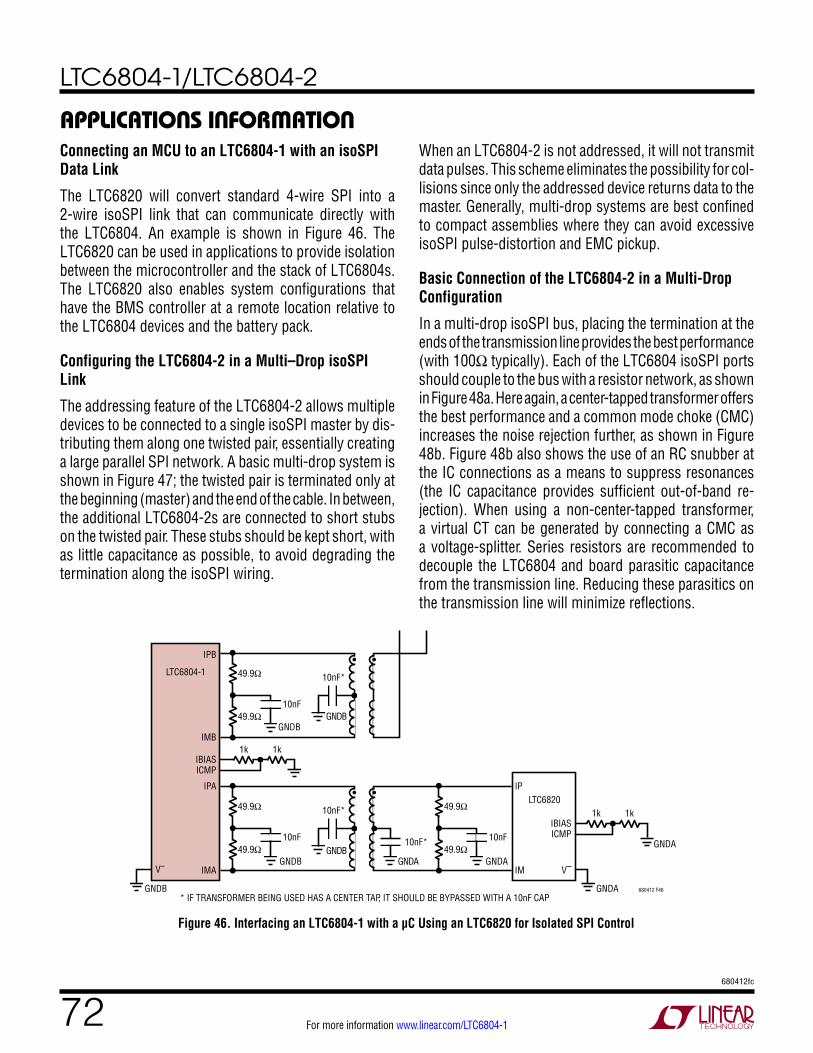
LTC6804-1/LTC6804-2
72680412fc
For more information www.linear.com/LTC6804-1
applicaTions inForMaTionWhen an LTC6804-2 is not addressed, it will not transmit data pulses. This scheme eliminates the possibility for col-lisions since only the addressed device returns data to the master. Generally, multi-drop systems are best confined to compact assemblies where they can avoid excessive isoSPI pulse-distortion and EMC pickup.
Basic Connection of the LTC6804-2 in a Multi-Drop Configuration
In a multi-drop isoSPI bus, placing the termination at the ends of the transmission line provides the best performance (with 100Ω typically). Each of the LTC6804 isoSPI ports should couple to the bus with a resistor network, as shown in Figure 48a. Here again, a center-tapped transformer offers the best performance and a common mode choke (CMC) increases the noise rejection further, as shown in Figure 48b. Figure 48b also shows the use of an RC snubber at the IC connections as a means to suppress resonances (the IC capacitance provides sufficient out-of-band re-jection). When using a non-center-tapped transformer, a virtual CT can be generated by connecting a CMC as a voltage-splitter. Series resistors are recommended to decouple the LTC6804 and board parasitic capacitance from the transmission line. Reducing these parasitics on the transmission line will minimize reflections.
Connecting an MCU to an LTC6804-1 with an isoSPI Data Link
The LTC6820 will convert standard 4-wire SPI into a 2-wire isoSPI link that can communicate directly with the LTC6804. An example is shown in Figure 46. The LTC6820 can be used in applications to provide isolation between the microcontroller and the stack of LTC6804s. The LTC6820 also enables system configurations that have the BMS controller at a remote location relative to the LTC6804 devices and the battery pack.
Configuring the LTC6804-2 in a Multi–Drop isoSPI Link
The addressing feature of the LTC6804-2 allows multiple devices to be connected to a single isoSPI master by dis-tributing them along one twisted pair, essentially creating a large parallel SPI network. A basic multi-drop system is shown in Figure 47; the twisted pair is terminated only at the beginning (master) and the end of the cable. In between, the additional LTC6804-2s are connected to short stubs on the twisted pair. These stubs should be kept short, with as little capacitance as possible, to avoid degrading the termination along the isoSPI wiring.
10nF
GNDB
GNDB
10nF
GNDA
GNDA10nF*
10nF*
10nF
GNDB
10nF*
1k 1k
1k 1k
••
GNDA
GNDB
••
GNDB
GNDA
49.9Ω
49.9Ω
49.9Ω
49.9Ω
IPA
IBIASICMP
IBIASICMP
LTC6804-1
IMA
49.9Ω
49.9Ω
IP
IM V–
IPB
IMB
* IF TRANSFORMER BEING USED HAS A CENTER TAP, IT SHOULD BE BYPASSED WITH A 10nF CAP680412 F46
LTC6820
V–
Figure 46. Interfacing an LTC6804-1 with a µC Using an LTC6820 for Isolated SPI Control
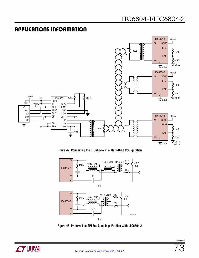
LTC6804-1/LTC6804-2
73680412fc
For more information www.linear.com/LTC6804-1
applicaTions inForMaTion
1.21k
806Ω
IPA
IBIAS
ISOMD
IMAV–
VREGB
ICMP
LTC6804-2
1.21k
806Ω
IPA
IBIAS
ISOMD
IMAV–
VREGA
ICMP
680412 F47
LTC6804-2
1.21k
806Ω
GNDB
GNDA
GNDC
GNDB
GNDA
GNDC
IPA
IBIAS
ISOMD
IMAV–
VREGC
ICMP
LTC6804-2
••
••
••••
100Ω
1.21k 806Ω
5k
100nF
IBIASICMPGND
SLOWMSTR
IPIM
VDD
VDDSENMOSIMISOSCKCS
POLPHA 5V5V
5V
5V
LTC6820100nF
µCSDO
CS
SDISCK
100Ω
Figure 47. Connecting the LTC6804-2 in a Multi-Drop Configuration
isoSPIBUS
HV XFMR
CT HV XFMR
22Ω
22Ω
22Ω
22Ω
isoSPIBUS
LTC6804-2
LTC6804-2
IPA
IMA
V–
15pF
100µH CMC
10nF
•
•100µH CMC
•
•402Ω
15pF
402Ω
••
a)
IPA
IMA
V–
100µH CMC
10nF
•
• ••
b)
680412 F48
Figure 48. Preferred isoSPI Bus Couplings For Use With LTC6804-2
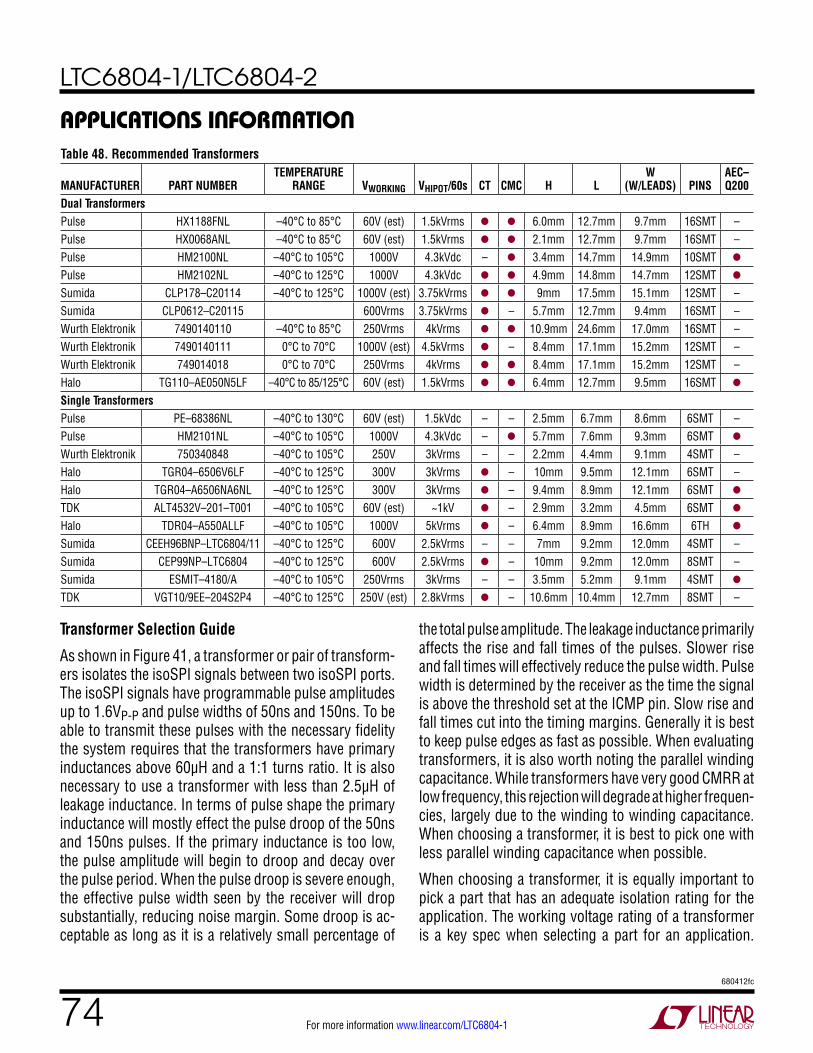
LTC6804-1/LTC6804-2
74680412fc
For more information www.linear.com/LTC6804-1
Transformer Selection Guide
As shown in Figure 41, a transformer or pair of transform-ers isolates the isoSPI signals between two isoSPI ports. The isoSPI signals have programmable pulse amplitudes up to 1.6VP-P and pulse widths of 50ns and 150ns. To be able to transmit these pulses with the necessary fidelity the system requires that the transformers have primary inductances above 60µH and a 1:1 turns ratio. It is also necessary to use a transformer with less than 2.5µH of leakage inductance. In terms of pulse shape the primary inductance will mostly effect the pulse droop of the 50ns and 150ns pulses. If the primary inductance is too low, the pulse amplitude will begin to droop and decay over the pulse period. When the pulse droop is severe enough, the effective pulse width seen by the receiver will drop substantially, reducing noise margin. Some droop is ac-ceptable as long as it is a relatively small percentage of
applicaTions inForMaTion
the total pulse amplitude. The leakage inductance primarily affects the rise and fall times of the pulses. Slower rise and fall times will effectively reduce the pulse width. Pulse width is determined by the receiver as the time the signal is above the threshold set at the ICMP pin. Slow rise and fall times cut into the timing margins. Generally it is best to keep pulse edges as fast as possible. When evaluating transformers, it is also worth noting the parallel winding capacitance. While transformers have very good CMRR at low frequency, this rejection will degrade at higher frequen-cies, largely due to the winding to winding capacitance. When choosing a transformer, it is best to pick one with less parallel winding capacitance when possible.
When choosing a transformer, it is equally important to pick a part that has an adequate isolation rating for the application. The working voltage rating of a transformer is a key spec when selecting a part for an application.
Table 48. Recommended Transformers
MANUFACTURER PART NUMBERTEMPERATURE
RANGE VWORKING VHIPOT/60s CT CMC H LW
(W/LEADS) PINSAEC–q200
Dual TransformersPulse HX1188FNL –40°C to 85°C 60V (est) 1.5kVrms l l 6.0mm 12.7mm 9.7mm 16SMT –Pulse HX0068ANL –40°C to 85°C 60V (est) 1.5kVrms l l 2.1mm 12.7mm 9.7mm 16SMT –Pulse HM2100NL –40°C to 105°C 1000V 4.3kVdc – l 3.4mm 14.7mm 14.9mm 10SMT l
Pulse HM2102NL –40°C to 125°C 1000V 4.3kVdc l l 4.9mm 14.8mm 14.7mm 12SMT l
Sumida CLP178–C20114 –40°C to 125°C 1000V (est) 3.75kVrms l l 9mm 17.5mm 15.1mm 12SMT –Sumida CLP0612–C20115 600Vrms 3.75kVrms l – 5.7mm 12.7mm 9.4mm 16SMT –Wurth Elektronik 7490140110 –40°C to 85°C 250Vrms 4kVrms l l 10.9mm 24.6mm 17.0mm 16SMT –Wurth Elektronik 7490140111 0°C to 70°C 1000V (est) 4.5kVrms l – 8.4mm 17.1mm 15.2mm 12SMT –Wurth Elektronik 749014018 0°C to 70°C 250Vrms 4kVrms l l 8.4mm 17.1mm 15.2mm 12SMT –Halo TG110–AE050N5LF –40°C to 85/125°C 60V (est) 1.5kVrms l l 6.4mm 12.7mm 9.5mm 16SMT l
Single TransformersPulse PE–68386NL –40°C to 130°C 60V (est) 1.5kVdc – – 2.5mm 6.7mm 8.6mm 6SMT –Pulse HM2101NL –40°C to 105°C 1000V 4.3kVdc – l 5.7mm 7.6mm 9.3mm 6SMT l
Wurth Elektronik 750340848 –40°C to 105°C 250V 3kVrms – – 2.2mm 4.4mm 9.1mm 4SMT –Halo TGR04–6506V6LF –40°C to 125°C 300V 3kVrms l – 10mm 9.5mm 12.1mm 6SMT –Halo TGR04–A6506NA6NL –40°C to 125°C 300V 3kVrms l – 9.4mm 8.9mm 12.1mm 6SMT l
TDK ALT4532V–201–T001 –40°C to 105°C 60V (est) ~1kV l – 2.9mm 3.2mm 4.5mm 6SMT l
Halo TDR04–A550ALLF –40°C to 105°C 1000V 5kVrms l – 6.4mm 8.9mm 16.6mm 6TH l
Sumida CEEH96BNP–LTC6804/11 –40°C to 125°C 600V 2.5kVrms – – 7mm 9.2mm 12.0mm 4SMT –Sumida CEP99NP–LTC6804 –40°C to 125°C 600V 2.5kVrms l – 10mm 9.2mm 12.0mm 8SMT –Sumida ESMIT–4180/A –40°C to 105°C 250Vrms 3kVrms – – 3.5mm 5.2mm 9.1mm 4SMT l
TDK VGT10/9EE–204S2P4 –40°C to 125°C 250V (est) 2.8kVrms l – 10.6mm 10.4mm 12.7mm 8SMT –
LTC6804-1/LTC6804-2
75680412fc
For more information www.linear.com/LTC6804-1
Interconnecting daisy-chain links between LTC6804-1 devices see <60V stress in typical applications; ordinary pulse and LAN type transformers will suffice. Multi-drop connections and connections to the LTC6820, in general, may need much higher working voltage ratings for good long-term reliability. Usually, matching the working voltage to the voltage of the entire battery stack is conservative. Unfortunately, transformer vendors will often only specify one-second HV testing, and this is not equal to the long-term (“permanent”) rating of the part. For example, according to most safety standards a 1.5kV rated transformer is expected to handle 230V continuously, and a 3kV device is capable of 1100V long-term, though manufacturers may not always certify to those levels (refer to actual vendor data for specifics). Usually, the higher voltage transformers are called “high-isolation” or “reinforced insulation” types by the suppliers. Table 48 shows a list of transformers that have been evaluated in isoSPI links.
In most applications a common mode choke is also necessary for noise rejection. Table 49 includes a list of suitable CMCs if the CMC is not already integrated into the transformer being used.
isoSPI Layout Guidelines
Layout of the isoSPI signal lines also plays a significant role in maximizing the noise immunity of a data link. The following layout guidelines are recommended:
1. The transformer should be placed as close to the isoSPI cable connector as possible. The distance should be kept less than 2cm. The LTC6804 should be placed close to but at least 1cm to 2cm away from the transformer to help isolate the IC from magnetic field coupling.
2. A V– ground plane should not extend under the trans-former, the isoSPI connector or in between the trans-former and the connector.
3. The isoSPI signal traces should be as direct as possible while isolated from adjacent circuitry by ground metal or space. No traces should cross the isoSPI signal lines, unless separated by a ground plane on an inner layer.
Table 49. Recommended Common Mode ChokesMANUFACTURER PART NUMBER
TDK ACT45B-101-2P
Murata DLW43SH101XK2
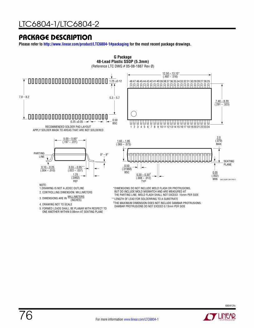
LTC6804-1/LTC6804-2
76680412fc
For more information www.linear.com/LTC6804-1
package DescripTionPlease refer to http://www.linear.com/product/LTC6804-1#packaging for the most recent package drawings.
0.10 – 0.25(.004 – .010)
0° – 8°
G48 (SSOP) 0910 REV 0
SEATINGPLANE
0.55 – 0.95**(.022 – .037)
1.25(.0492)
REF
5.00 – 5.60*(.197 – .221)
7.40 – 8.20(.291 – .323)
1 2 3 4 5 6 7 8 9 10 11 12 14 15 16 17 18 19 20 21 2223 2413
4445464748 43 42 41 40 39 38 37 36 35 34 33 31 30 29 28 27 26 2532
12.50 – 13.10*(.492 – .516)
2.0(.079)MAX
1.65 – 1.85(.065 – .073)
0.05(.002)MIN
0.50(.01968)
BSC0.20 – 0.30†
(.008 – .012)TYP
MILLIMETERS(INCHES)
DIMENSIONS DO NOT INCLUDE MOLD FLASH OR PROTRUSIONS,BUT DO INCLUDE MOLD MISMATCH AND ARE MEASURED ATTHE PARTING LINE. MOLD FLASH SHALL NOT EXCEED .15mm PER SIDELENGTH OF LEAD FOR SOLDERRING TO A SUBSTRATETHE MAXIMUM DIMENSION DOES NOT INCLUDE DAMBAR PROTRUSIONS.DAMBAR PROTRUSIONS DO NOT EXCEED 0.13mm PER SIDE
*
**†
NOTE:1.DRAWING IS NOT A JEDEC OUTLINE2. CONTROLLING DIMENSION: MILLIMETERS
3. DIMENSIONS ARE IN
4. DRAWING NOT TO SCALE5. FORMED LEADS SHALL BE PLANAR WITH RESPECT TO ONE ANOTHER WITHIN 0.08mm AT SEATING PLANE
0.25 ±0.05
PARTINGLINE
0.50BSC
5.3 – 5.77.8 – 8.2
RECOMMENDED SOLDER PAD LAYOUTAPPLY SOLDER MASK TO AREAS THAT ARE NOT SOLDERED
1.25 ±0.12
G Package48-Lead Plastic SSOP (5.3mm)
(Reference LTC DWG # 05-08-1887 Rev Ø)
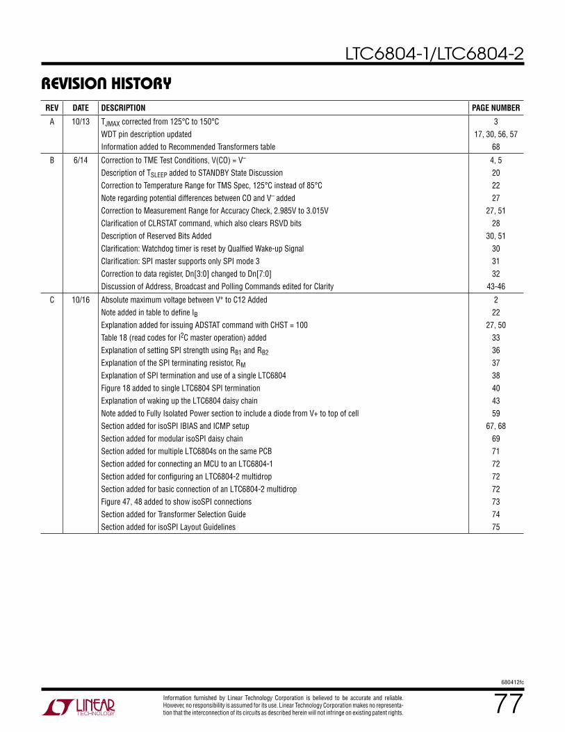
LTC6804-1/LTC6804-2
77680412fc
For more information www.linear.com/LTC6804-1
Information furnished by Linear Technology Corporation is believed to be accurate and reliable. However, no responsibility is assumed for its use. Linear Technology Corporation makes no representa-tion that the interconnection of its circuits as described herein will not infringe on existing patent rights.
revision hisToryREV DATE DESCRIPTION PAGE NUMBER
A 10/13 TJMAX corrected from 125°C to 150°CWDT pin description updatedInformation added to Recommended Transformers table
317, 30, 56, 57
68
B 6/14 Correction to TME Test Conditions, V(CO) = V–
Description of TSLEEP added to STANDBY State DiscussionCorrection to Temperature Range for TMS Spec, 125°C instead of 85°CNote regarding potential differences between CO and V– addedCorrection to Measurement Range for Accuracy Check, 2.985V to 3.015VClarification of CLRSTAT command, which also clears RSVD bitsDescription of Reserved Bits AddedClarification: Watchdog timer is reset by Qualfied Wake-up SignalClarification: SPI master supports only SPI mode 3Correction to data register, Dn[3:0] changed to Dn[7:0]Discussion of Address, Broadcast and Polling Commands edited for Clarity
4, 5202227
27, 5128
30, 51303132
43-46
C 10/16 Absolute maximum voltage between V+ to C12 AddedNote added in table to define IBExplanation added for issuing ADSTAT command with CHST = 100Table 18 (read codes for I2C master operation) addedExplanation of setting SPI strength using RB1 and RB2
Explanation of the SPI terminating resistor, RM
Explanation of SPI termination and use of a single LTC6804Figure 18 added to single LTC6804 SPI terminationExplanation of waking up the LTC6804 daisy chainNote added to Fully Isolated Power section to include a diode from V+ to top of cellSection added for isoSPI IBIAS and ICMP setupSection added for modular isoSPI daisy chainSection added for multiple LTC6804s on the same PCBSection added for connecting an MCU to an LTC6804-1Section added for configuring an LTC6804-2 multidropSection added for basic connection of an LTC6804-2 multidropFigure 47, 48 added to show isoSPI connectionsSection added for Transformer Selection GuideSection added for isoSPI Layout Guidelines
222
27, 5033363738404359
67, 686971727272737475
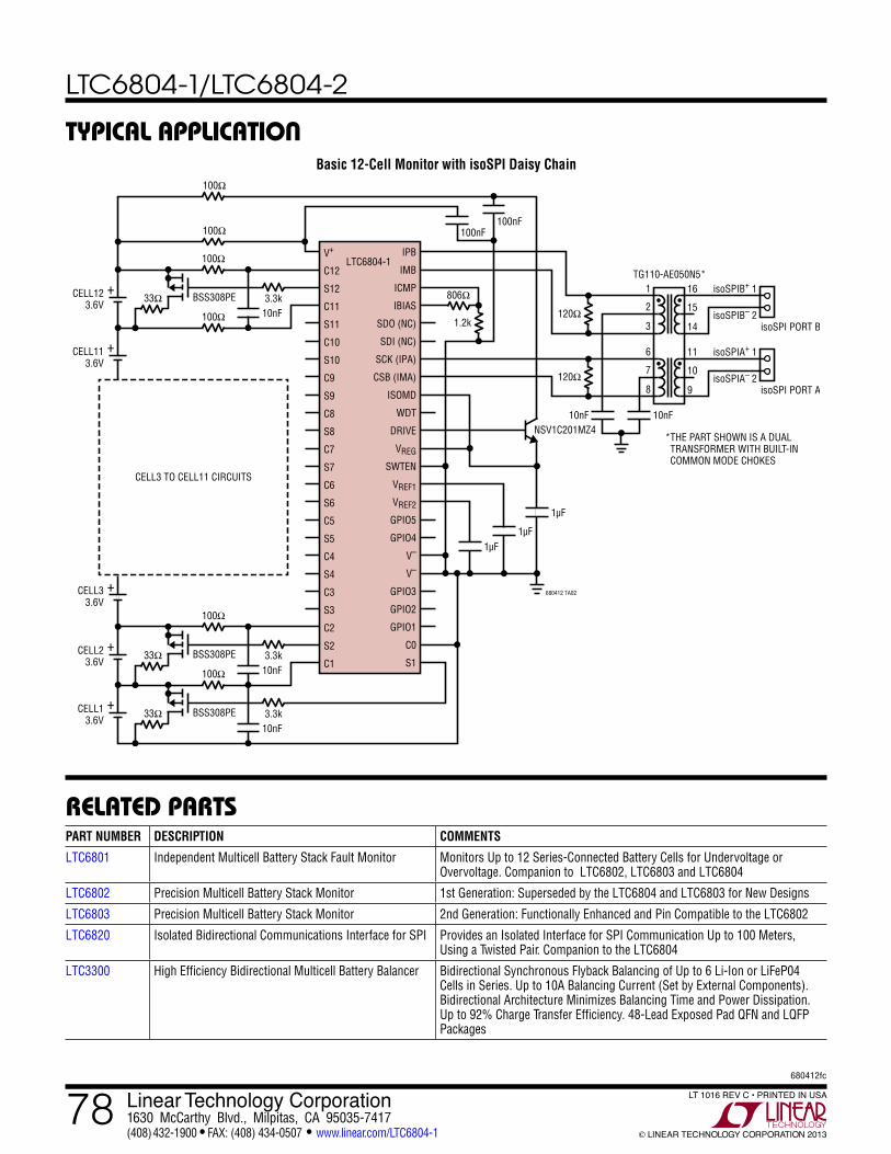
LTC6804-1/LTC6804-2
78680412fc
For more information www.linear.com/LTC6804-1 LINEAR TECHNOLOGY CORPORATION 2013
LT 1016 REV C • PRINTED IN USALinear Technology Corporation1630 McCarthy Blvd., Milpitas, CA 95035-7417(408) 432-1900 ● FAX: (408) 434-0507 ● www.linear.com/LTC6804-1
relaTeD parTs
Typical applicaTion
PART NUMBER DESCRIPTION COMMENTS
LTC6801 Independent Multicell Battery Stack Fault Monitor Monitors Up to 12 Series-Connected Battery Cells for Undervoltage or Overvoltage. Companion to LTC6802, LTC6803 and LTC6804
LTC6802 Precision Multicell Battery Stack Monitor 1st Generation: Superseded by the LTC6804 and LTC6803 for New Designs
LTC6803 Precision Multicell Battery Stack Monitor 2nd Generation: Functionally Enhanced and Pin Compatible to the LTC6802
LTC6820 Isolated Bidirectional Communications Interface for SPI Provides an Isolated Interface for SPI Communication Up to 100 Meters, Using a Twisted Pair. Companion to the LTC6804
LTC3300 High Efficiency Bidirectional Multicell Battery Balancer Bidirectional Synchronous Flyback Balancing of Up to 6 Li-Ion or LiFeP04 Cells in Series. Up to 10A Balancing Current (Set by External Components). Bidirectional Architecture Minimizes Balancing Time and Power Dissipation. Up to 92% Charge Transfer Efficiency. 48-Lead Exposed Pad QFN and LQFP Packages
Basic 12-Cell Monitor with isoSPI Daisy Chain
680412 TA02
V+
C12
S12
C11
S11
C10
S10
C9
S9
C8
S8
C7
S7
C6
S6
C5
S5
C4
S4
C3
S3
C2
S2
C1
IPB
IMB
ICMP
IBIAS
SDO (NC)
SDI (NC)
SCK (IPA)
CSB (IMA)
ISOMD
WDT
DRIVE
VREG
SWTEN
VREF1
VREF2
GPIO5
GPIO4
V–
V–
GPIO3
GPIO2
GPIO1
C0
S1
LTC6804-1
107
6
8 9
11
isoSPIA–
isoSPI PORT A
TG110-AE050N5*
isoSPIA+
2
1
806Ω
1.2k
CELL23.6V
10nF
100Ω
BSS308PE33Ω 3.3k
CELL13.6V
CELL33.6V
10nF
100Ω
BSS308PE33Ω 3.3k+
+
+
CELL123.6V
10nF
100Ω
BSS308PE33Ω
100Ω
100Ω
3.3k
CELL113.6V
100Ω
CELL3 TO CELL11 CIRCUITS
1µF
100nF100nF
1µF
1µF
120Ω
152
1
3 14
16
isoSPIB–
isoSPI PORT B
isoSPIB+
2
1
120Ω
10nF
*THE PART SHOWN IS A DUAL TRANSFORMER WITH BUILT-IN COMMON MODE CHOKES
10nF
••
••+
+
NSV1C201MZ4