lte full-band ceramic chip antenna model: cc40d9 product
TRANSCRIPT
Unique Electronics You Need Version: 10606A_revB
LTE Full-Band Ceramic Chip Antenna Model: CC40D9
Product Number: H2UE3P1D2G0100
REFERENCE SPECIFICATION

Datasheet:CC40D9 -H2UE3P1D2G0100
Page 2 / 22 Unique Electronics You Need
Table of Contents 1 Introduction ......................................................................................................................................... 3
2 Electrical Characteristics ...................................................................................................................... 4
2.1 Table with electrical properties: .................................................................................................. 4
2.2 Return Loss (S11) .......................................................................................................................... 5
2.3 VSWR (S11).................................................................................................................................... 5
2.4 3D Efficiency Table for 698~960 MHz Band ................................................................................ 6
2.6 3D Efficiency Table for 1710~2170 MHz Band ............................................................................ 7
2.8 3D Efficiency Table for 2300~2400 MHz Band ............................................................................ 8
2.10 3D Efficiency Table for 2490~2690 MHz Band ............................................................................ 9
2.12 Radiation Pattern (with 120 x 45mm2 Evaluation Board) ......................................................... 10
3 Layout Guide ...................................................................................................................................... 15
3.1 Layout Guide (Unit: mm) Solder Land Pattern: ......................................................................... 15
3.2 Outline Dimensions of Antenna & Evaluation Board ................................................................ 16
3.3 Frequency tuning and Matching circuit ..................................................................................... 18
4 Packing ............................................................................................................................................... 19
5 Notes .................................................................................................................................................. 20
5.1 Soldering Conditions ................................................................................................................. 20
5.2 Reminders ................................................................................................................................. 20
5.3 Operating & Storage Conditions ............................................................................................... 20
Introduction Electrical Characteristics Radiation Pattern Layout Tuning Packing Notes

Datasheet:CC40D9 -H2UE3P1D2G0100
Page 3 / 22 Unique Electronics You Need
1 Introduction
Unictron’s CC40D9 ceramic chip antenna is designed to cover the full cellular
2G / 3G / GSM / 4G / LTE bands, covering frequencies 698~960 MHz & 1710~2690
MHz. Fabricated with proprietary design and processes, CC40D9 delivers excellent
performance and is fully compatible with SMT processes which decreases the
assembly cost and improve device’s quality and consistency.
Features
* LTE full-band coverage
* High efficiency
* Stable and reliable in performances
* Compact size
* RoHS compliance
* SMT processes compatible
Applications
* LTE / GSM / CDMA / DCS / PCS
WCDMA / UMTS / HSDPA / GPRS
EDGE / IMT
* Cellular 4G / 3G / 2G applications
Introduction Electrical Characteristics Radiation Pattern Layout Tuning Packing Notes

Datasheet:CC40D9 -H2UE3P1D2G0100
Page 4 / 22 Unique Electronics You Need
2 Electrical Characteristics
2.1 Table with electrical properties:
Electrical Specifications (Evaluation Board Dimensions: 120 x 45mm2)
Electrical Table
Characteristics Specifications Unit
Outline Dimensions 40.0 x 5.0 x 6.0 mm
Ground Plane Dimensions 107 x 45 mm
Working Frequency
698 |
798
824 |
960
1710 |
2170
2300 |
2400
2490 |
2690 MHz
Peak Gain 1.4 1.1 3.2 3.8 4.2 dBi
Efficiency 65 61 71 67 62 %
VSWR* < 3.0 : 1 (typical)
Characteristic Impedance 50 Ω
Polarization Linear Polarization
*Center frequency means the frequency with the lowest value in return loss of the chip antenna on
the evaluation board.
Introduction Electrical Characteristics Radiation Pattern Layout Tuning Packing Notes
Datasheet:CC40D9 -H2UE3P1D2G0100
Page 5 / 22 Unique Electronics You Need
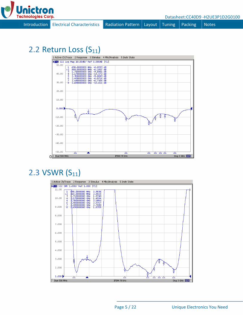
2.2 Return Loss (S11)
0
2.3 VSWR (S11)
Introduction Electrical Characteristics Radiation Pattern Layout Tuning Packing Notes Introduction Electrical Characteristics Radiation Pattern Layout Tuning Packing Notes

Datasheet:CC40D9 -H2UE3P1D2G0100
Page 6 / 22 Unique Electronics You Need
2.4 3D Efficiency Table for 698~960 MHz Band
Frequency(MHz) 698 720 740 760 780 800 824 840 860 880 900 920 940 960
Efficiency(dB) -2.6 -1.9 -1.5 -1.5 -1.6 -1.8 -2.0 -2.4 -2.4 -2.4 -2.1 -2.0 -2.0 -2.0
Efficiency(%) 54.4 65.0 71.0 70.3 69.0 65.9 63.3 57.5 57.1 57.6 61.2 62.7 63.1 63.5
Gain(dBi) 0.5 1.0 1.8 1.9 1.7 1.5 1.4 1.1 0.8 0.8 1.0 1.1 1.2 1.4
3D Efficiency vs. Frequency 698~960 MHz Band
Introduction Electrical Characteristics Radiation Pattern Layout Tuning Packing Notes

Datasheet:CC40D9 -H2UE3P1D2G0100
Page 7 / 22 Unique Electronics You Need
2.5 3D Efficiency Table for 1710~2170 MHz Band
Frequency(MHz) 1710 1740 1770 1800 1830 1860 1890 1920 1950 1980 2010 2040 2070 2100 2130 2170
Efficiency(dB) -2.0 -1.4 -1.3 -1.1 -1.2 -1.4 -1.5 -1.8 -1.7 -1.7 -1.8 -1.8 -1.9 -2.0 -2.0 -2.2
Efficiency(%) 63.4 72.2 74.4 78.2 76.2 71.9 70.3 66.2 68.0 67.2 66.2 66.1 64.2 63.1 62.9 60.3
Gain(dBi) 3.6 4.0 4.0 4.0 3.9 3.8 3.9 3.6 3.8 3.6 3.2 3.2 2.7 2.7 2.9 3.6
3D Efficiency vs. Frequency 1710~2170 MHz Band
Introduction Electrical Characteristics Radiation Pattern Layout Tuning Packing Notes
Datasheet:CC40D9 -H2UE3P1D2G0100
Page 8 / 22 Unique Electronics You Need
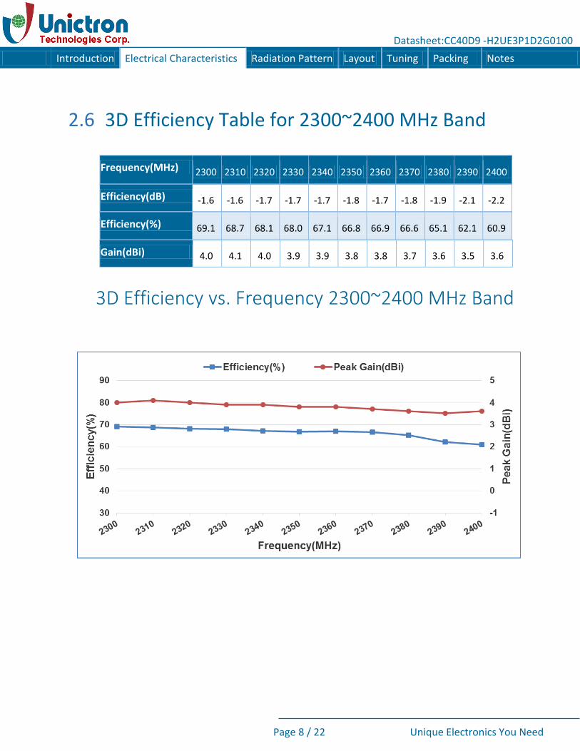
2.6 3D Efficiency Table for 2300~2400 MHz Band
Frequency(MHz) 2300 2310 2320 2330 2340 2350 2360 2370 2380 2390 2400
Efficiency(dB) -1.6 -1.6 -1.7 -1.7 -1.7 -1.8 -1.7 -1.8 -1.9 -2.1 -2.2
Efficiency(%) 69.1 68.7 68.1 68.0 67.1 66.8 66.9 66.6 65.1 62.1 60.9
3D Efficiency vs. Frequency 2300~2400 MHz Band
Gain(dBi) 4.0 4.1 4.0 3.9 3.9 3.8 3.8 3.7 3.6 3.5 3.6
Introduction Electrical Characteristics Radiation Pattern Layout Tuning Packing Notes

Datasheet:CC40D9 -H2UE3P1D2G0100
Page 9 / 22 Unique Electronics You Need
2.7 3D Efficiency Table for 2490~2690 MHz Band
Frequency(MHz) 2490 2510 2530 2550 2570 2590 2610 2630 2650 2670 2690
Efficiency(dB) -2.2 -2.0 -2.0 -1.9 -1.9 -1.9 -1.7 -1.5 -1.5 -1.5 -1.5
Efficiency(%) 60.6 63.1 62.8 63.9 63.9 64.0 68.1 70.4 71.0 71.0 71.4
3D Efficiency vs. Frequency 2490~2690 MHz Band
Gain(dBi) 2.3 2.9 2.7 3.2 3.2 3.3 3.0 3.3 3.6 3.7 3.8
Introduction Electrical Characteristics Radiation Pattern Layout Tuning Packing Notes

Datasheet:CC40D9 -H2UE3P1D2G0100
Page 10 / 22 Unique Electronics You Need
2.8 Radiation Pattern (with 120 x 45mm2 Evaluation Board)
698~798MHz Band
3D Gain Pattern @ 748 MHz (Unit: dBi)
Introduction Electrical Characteristics Radiation Pattern Layout Tuning Packing Notes
Y

Datasheet:CC40D9 -H2UE3P1D2G0100
Page 11 / 22 Unique Electronics You Need
2.9 Radiation Pattern (with 120 x 45mm2 Evaluation Board)
824~960 MHz Band
3D Gain Pattern @ 900 MHz (Unit: dBi)
Introduction Electrical Characteristics Radiation Pattern Layout Tuning Packing Notes

Datasheet:CC40D9 -H2UE3P1D2G0100
Page 12 / 22 Unique Electronics You Need
2.10 Radiation Pattern (with 120 x 45mm2 Evaluation Board)
1710~2170 MHz Band 3D Gain Pattern @ 1950 MHz (Unit: dBi)
Introduction Electrical Characteristics Radiation Pattern Layout Tuning Packing Notes
Datasheet:CC40D9 -H2UE3P1D2G0100
Page 13 / 22 Unique Electronics You Need
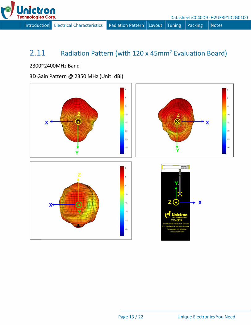
2.11 Radiation Pattern (with 120 x 45mm2 Evaluation Board)
2300~2400MHz Band
3D Gain Pattern @ 2350 MHz (Unit: dBi)
Introduction Electrical Characteristics Radiation Pattern Layout Tuning Packing Notes

Datasheet:CC40D9 -H2UE3P1D2G0100
Page 14 / 22 Unique Electronics You Need
2.12 Radiation Pattern (with 120 x 45mm2 Evaluation Board)
2490~2690MHz Band
3D Gain Pattern @ 2590 MHz (Unit: dBi)
Introduction Electrical Characteristics Radiation Pattern Layout Tuning Packing Notes Introduction Electrical Characteristics Radiation Pattern Layout Tuning Packing Notes Introduction Electrical Characteristics Radiation Pattern Layout Tuning Packing Notes

Datasheet:CC40D9 -H2UE3P1D2G0100
Page 15 / 22 Unique Electronics You Need
3 Layout Guide 3.1 Layout Guide (Unit: mm)
Solder Land Pattern: The solder land pattern (golden marking areas) is shown in below figures. Depending
on Customer’s requirement, an additional matching circuit is normally required.
Introduction Electrical Characteristics Radiation Pattern Layout Tuning Packing Notes Introduction Electrical Characteristics Radiation Pattern Layout Tuning Packing Notes

Datasheet:CC40D9 -H2UE3P1D2G0100
Page 16 / 22 Unique Electronics You Need
3.2 Outline Dimensions of Antenna & Evaluation Board
3.2.1 Antenna Dimensions
Introduction Electrical Characteristics Radiation Pattern Layout Tuning Packing Notes
Datasheet:CC40D9 -H2UE3P1D2G0100
Page 17 / 22 Unique Electronics You Need
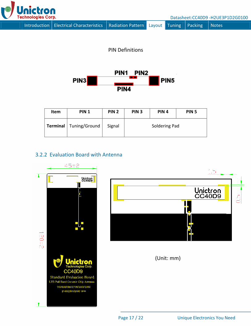
PIN Definitions
3.2.2 Evaluation Board with Antenna
(Unit: mm)
Item PIN 1 PIN 2 PIN 3 PIN 4 PIN 5
Terminal Tuning/Ground Signal Soldering Pad
Introduction Electrical Characteristics Radiation Pattern Layout Tuning Packing Notes

Datasheet:CC40D9 -H2UE3P1D2G0100
Page 18 / 22 Unique Electronics You Need
3.3 Frequency tuning and Matching circuit 3.3.1 Chip antenna tuning scenario
3.3.2 Matching circuit
With the following recommended values of matching and tuning components, the covering frequencies will be about 698~960 MHz & 1710~2690 MHz at our standard 120 x 45 mm2 evaluation board. However, these are typical reference values which may need to be changed when circuit boards or part vendors are different.
Introduction Electrical Characteristics Radiation Pattern Layout Tuning Packing Notes Introduction Electrical Characteristics Radiation Pattern Layout Tuning Packing Notes Introduction Electrical Characteristics Radiation Pattern Layout Tuning Packing Notes Introduction

Datasheet:CC40D9 -H2UE3P1D2G0100
Page 19 / 22 Unique Electronics You Need
4 Packing
(1) Quantity/Reel: 600 pcs/Reel
(2) Plastic tape: Clear Non Anti-static Polystyrene
Introduction Electrical Characteristics Radiation Pattern Layout Tuning Packing Notes
Datasheet:CC40D9 -H2UE3P1D2G0100
Page 20 / 22 Unique Electronics You Need
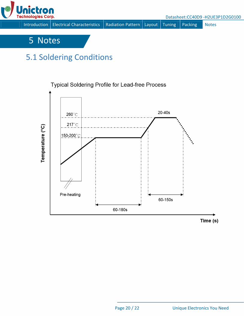
5 Notes
5.1 Soldering Conditions
Introduction Electrical Characteristics Radiation Pattern Layout Tuning Packing Notes

Datasheet:CC40D9 -H2UE3P1D2G0100
Page 21 / 22 Unique Electronics You Need
5.2 Reminders for users of Unictron’s CC40D9 ceramic chip antennas 5.2.1 This chip antenna is made of ceramic materials which is relatively more rigid and brittle compared to circuit board materials. Furthermore, the length of this antenna is quite long. Bending of circuit board at the locations where chip antenna is mounted may cause the cracking of solder joints or antenna itself. 5.2.2 Punching/cutting of the break-off tab of PCB panel may cause severe bending of the circuit board which may result in cracking of solder joints or chip antenna itself. Therefore break-off tab shall be located away from the installation site of chip antenna. 5.2.3 Be cautious when ultrasonic welding process needs to be used near the locations where chip antennas are installed. Strong ultrasonic vibration may cause the cracking of chip antenna solder joints.
5.3 Operating & Storage Conditions 5.3.1 Operating (1) Maximum Input Power: 2 W (2) Operating Temperature: -40 to 85
5.3.2 Storage (1) Storage Temperature: -5 to 40
(2) Relative Humidity: 20% to 70% (3) Shelf Life: 1 year 5.3.3 Notice (1) Installation Guide: Please refer to “General guidelines for the installation of Unictron’s chip antennas” document. (2) All specifications are subject to change without notice.
Introduction Electrical Characteristics Radiation Pattern Layout Tuning Packing Notes Introduction Electrical Characteristics Radiation Pattern Layout Tuning Packing Notes

Datasheet:CC40D9 -H2UE3P1D2G0100
Page 22 / 22 Unique Electronics You Need
Presented data were measured on reference PCB (ground) as shown in this specification. When the antenna placement or size of the PCB is changed, antenna performance and values of matching components may differ from data shown here.
Information presented in this Reference Specification is believed to be correct as
of the date of publishing. Unictron Technologies Corporation reserves the rights to
change the Reference Specification without notice due to technical improvements,
etc. Please consult with Unictron’s engineering team about the latest information
before using this product. Per request, we may provide advice and assistance in
implementing this antenna to a customer’s device by simulation or real
measurement of the interested device in our testing facilities.
Unictron Technologies Corporation
No. 41 Shuei-Keng, Guan-Si
Hsinchu 30648
Taiwan (R.O.C.)
Tel: +886-3-547-5550
Email: [email protected]
Web: www.unictron.com
Introduction Electrical Characteristics Radiation Pattern Layout Tuning Packing Notes