ltr-553als-wa product data sheet optical sensor...property of lite -on o nly part no.: ltr -553als...
TRANSCRIPT

LITE-ON DCC
RELEASE
LITE-ON Technology Corp. / OptoelectronicsNo.90,Chien 1 Road, Chung Ho, New Taipei City 23585, Taiwan, R.O.C.
Tel: 886-2-2222-6181 Fax: 886-2-2221-1948 / 886-2-2221-0660http://www.liteon.com/opto
Optical SensorProduct Data SheetLTR-553ALS-WA Spec No.: DS86-2013-0005Effective Date: 06/28/2013
Revision: -
BNS-OD-FC001/A4
BNS-OD-FC001/A4
BNS-OD-FC001/A4
BNS-OD-FC001/A4
Property of Lite-On Only
Part No.: LTR-553ALS-WA DATA SHEET Page: 1 of 41 BNS-OD-C131/A4 - Rev 1.1
1. Description
The LTR-553ALS-WA is an integrated low voltage I2C digital light sensor [ALS] and proximity sensor
[PS] with built-in emitter, in a single miniature chipled lead-free surface mount package. This sensor
converts light intensity to a digital output signal capable of direct I2C interface. It provides a linear
response over a wide dynamic range from 0.01 lux to 64k lux and is well suited to applications under
high ambient brightness. With built-in proximity sensor (emitter and detector), LTR-553ALS-WA offers
the feature to detect object at a user configurable distance.
The sensor supports an interrupt feature that removes the need to poll the sensor for a reading which
improves system efficiency. The sensor also supports several features that help to minimize the
occurrence of false triggering. This CMOS design and factory-set one time trimming capability ensure
minimal sensor-to-sensor variations for ease of manufacturability to the end customers.
2. Features
I2C interface (Fast Mode @ 400kbit/s)
Ultra-small ChipLED package
Built-in temperature compensation circuit
Low active power consumption with standby mode
Supply voltage range from 2.4V to 3.6V capable of 1.7V logic voltage
Operating temperature range from -30C to +70C
RoHS and Halogen free compliant
Light Sensor
Close to human eye spectral response
Immunity to IR / UV Light Source
Automatically rejects 50 / 60 Hz lightings flicker
6 dynamic range from 0.01 lux to 64k lux
16-bit effective resolution
Proximity Sensor
Built-in LED driver, emitter and detector
Programmable LED drive settings
11-bit effective resolution
High ambient light suppression
Property of Lite-On Only
Part No.: LTR-553ALS-WA DATA SHEET Page: 2 of 41 BNS-OD-C131/A4 - Rev 1.1
3. Applications
To control display backlight in
Mobile Devices: Mobile phone, PDA
Computing Devices: Notebook PC, Desktop Monitor
Consumer Devices: LCD/PDP TV backlight systems, Cameras, Personal Navigation Device,
Digital Photo Frame
Dashboard
4. Ordering Information
Part Number Packaging Type Package Quantity
LTR-553ALS-WA Tape and Reel 8-pins chipled package 8000
Property of Lite-On Only
Part No.: LTR-553ALS-WA DATA SHEET Page: 3 of 41 BNS-OD-C131/A4 - Rev 1.1
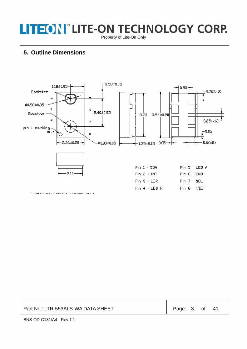
5. Outline Dimensions
Notes:
1. All dimensions are in millimeters
Property of Lite-On Only
Part No.: LTR-553ALS-WA DATA SHEET Page: 4 of 41 BNS-OD-C131/A4 - Rev 1.1
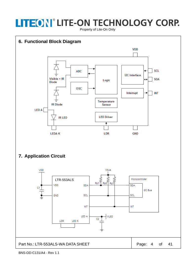
6. Functional Block Diagram
7. Application Circuit
LTR-553ALS
Property of Lite-On Only
Part No.: LTR-553ALS-WA DATA SHEET Page: 5 of 41 BNS-OD-C131/A4 - Rev 1.1
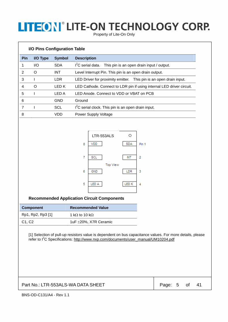
I/O Pins Configuration Table
Pin I/O Type Symbol Description
1 I/O SDA I2C serial data. This pin is an open drain input / output.
2 O INT Level Interrupt Pin. This pin is an open drain output.
3 I LDR LED Driver for proximity emitter. This pin is an open drain input.
4 O LED K LED Cathode. Connect to LDR pin if using internal LED driver circuit.
5 I LED A LED Anode. Connect to VDD or VBAT on PCB
6 GND Ground
7 I SCL I2C serial clock. This pin is an open drain input.
8 VDD Power Supply Voltage
Recommended Application Circuit Components
Component Recommended Value
Rp1, Rp2, Rp3 [1] 1 k to 10 k
C1, C2 1uF 20%, X7R Ceramic
[1] Selection of pull-up resistors value is dependent on bus capacitance values. For more details, please
refer to I2C Specifications: http://www.nxp.com/documents/user_manual/UM10204.pdf
LTR-553ALS

Property of Lite-On Only
Part No.: LTR-553ALS-WA DATA SHEET Page: 6 of 41 BNS-OD-C131/A4 - Rev 1.1
8. Rating and Specification
Absolute Maximum Ratings at Ta = 25C
Parameter Symbol Rating Unit
Supply Voltage VDD 3.8 V
Digital Voltage Range SCL, SDA, INT -0.5 to 3.8
V
Digital Output Current SCL, SDA, INT -1 to 20 mA
Storage Temperature Tstg -40 to 100 C
Note: Exceeding these ratings could cause damage to the sensor. All voltages are with respect to
ground. Currents are positive into, negative out of the specified terminal.
Recommended Operating Conditions
Description Symbol Min. Typ. Max. Unit
Supply Voltage VDD 2.4 3.6 V
LED Supply Voltage VLED 2.5 4.35 V
Interface Bus Power Supply Voltage VIO 1.7 3.6 V
Operating Temperature Tope -30 70 C
Electrical & Optical Specifications
All specifications are at VDD = 3.0V, Tope = 25C, unless otherwise noted.
Parameter Min. Typ. Max. Unit Condition
Active Supply Current 250 uA Active Mode, Tope = 25C
Standby Current 5 uA Standby / Sleep Mode
Initial Startup Time 60 100 1000 ms (Note 1)
Wakeup Time from Standby
10 ms (Note 1)
Light Sensor
Property of Lite-On Only
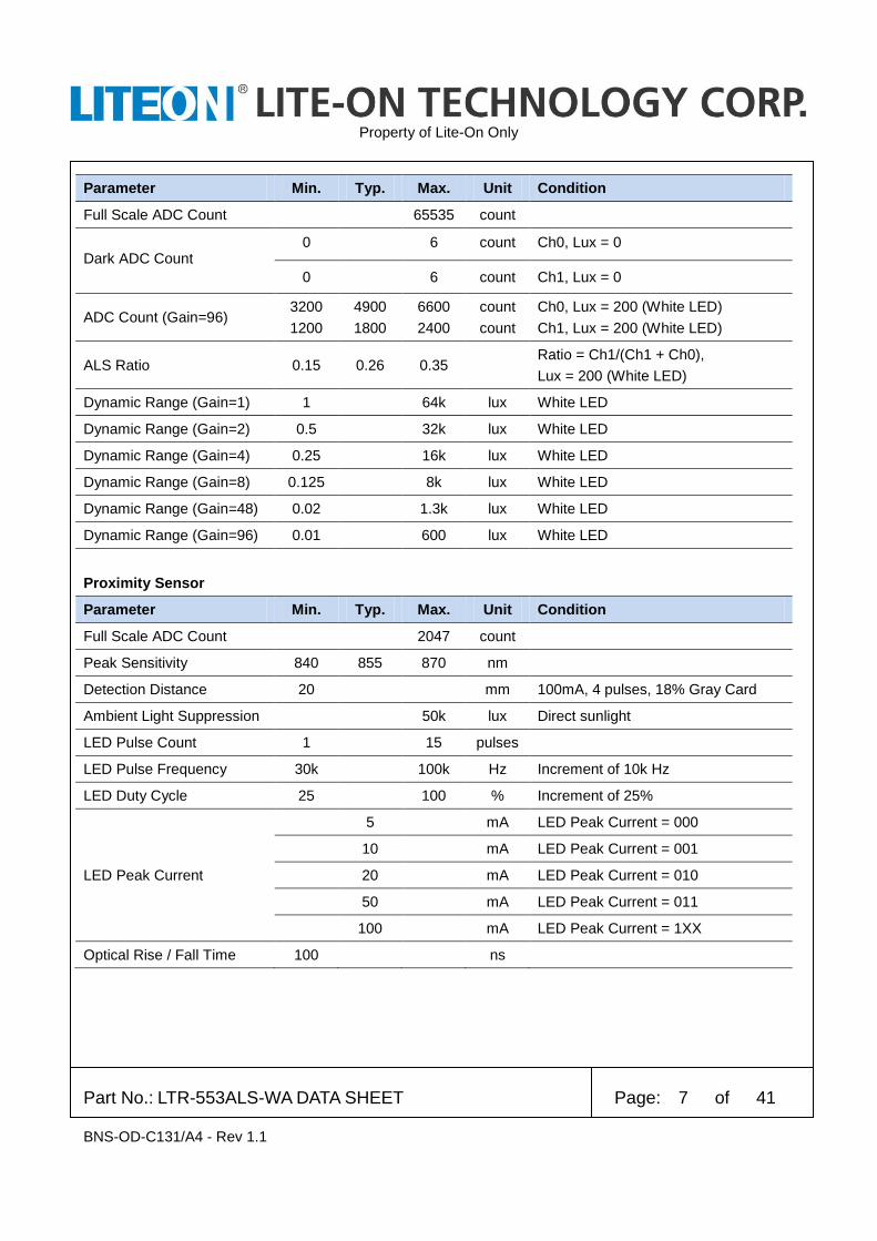
Part No.: LTR-553ALS-WA DATA SHEET Page: 7 of 41 BNS-OD-C131/A4 - Rev 1.1
Parameter Min. Typ. Max. Unit Condition
Full Scale ADC Count 65535 count
Dark ADC Count 0 6 count Ch0, Lux = 0
0 6 count Ch1, Lux = 0
ADC Count (Gain=96) 3200
1200
4900
1800
6600
2400
count
count
Ch0, Lux = 200 (White LED)
Ch1, Lux = 200 (White LED)
ALS Ratio 0.15 0.26 0.35 Ratio = Ch1/(Ch1 + Ch0),
Lux = 200 (White LED)
Dynamic Range (Gain=1) 1 64k lux White LED
Dynamic Range (Gain=2) 0.5 32k lux White LED
Dynamic Range (Gain=4) 0.25 16k lux White LED
Dynamic Range (Gain=8) 0.125 8k lux White LED
Dynamic Range (Gain=48) 0.02 1.3k lux White LED
Dynamic Range (Gain=96) 0.01 600 lux White LED
Proximity Sensor
Parameter Min. Typ. Max. Unit Condition
Full Scale ADC Count 2047 count
Peak Sensitivity 840 855 870 nm
Detection Distance 20 mm 100mA, 4 pulses, 18% Gray Card
Ambient Light Suppression 50k lux Direct sunlight
LED Pulse Count 1 15 pulses
LED Pulse Frequency 30k 100k Hz Increment of 10k Hz
LED Duty Cycle 25 100 % Increment of 25%
LED Peak Current
5 mA LED Peak Current = 000
10 mA LED Peak Current = 001
20 mA LED Peak Current = 010
50 mA LED Peak Current = 011
100 mA LED Peak Current = 1XX
Optical Rise / Fall Time 100 ns
Property of Lite-On Only
Part No.: LTR-553ALS-WA DATA SHEET Page: 8 of 41 BNS-OD-C131/A4 - Rev 1.1
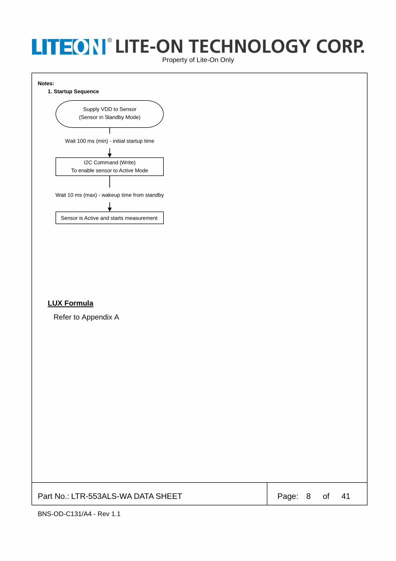
Notes:
1. Startup Sequence
LUX Formula
Refer to Appendix A
Supply VDD to Sensor
(Sensor in Standby Mode)
I2C Command (Write)
To enable sensor to Active Mode
Wait 100 ms (min) - initial startup time
Sensor is Active and starts measurement
Wait 10 ms (max) - wakeup time from standby

Property of Lite-On Only
Part No.: LTR-553ALS-WA DATA SHEET Page: 9 of 41 BNS-OD-C131/A4 - Rev 1.1
AC Electrical Characteristics
All specifications are at VBus = 1.8V, Tope = 25C, unless otherwise noted.
Parameter Symbol Min. Max. Unit
SCL clock frequency SCL
f 1 400 kHz
Bus free time between a STOP and START condition BUF
t 1.3 us
Hold time (repeated) START condition. After this period, the first clock pulse is generated
STAHDt
; 0.6 us
LOW period of the SCL clock LOW
t 1.3 us
HIGH period of the SCL clock HIGH
t 0.6 us
Set-up time for a repeated START condition STASUt
; 0.6 us
Set-up time for STOP condition STOSUt
; 0.6 us
Rise time of both SDA and SCL signals r
t 30 300 ns
Fall time of both SDA and SCL signals ft 30 300 ns
Data hold time DATHDt
; 0.3 0.9 us
Data setup time DATSUt
; 100 ns
Pulse width of spikes which must be suppressed by the input filter
SPt 0 50 ns
Definition of timing for I2C bus
Property of Lite-On Only
Part No.: LTR-553ALS-WA DATA SHEET Page: 10 of 41 BNS-OD-C131/A4 - Rev 1.1
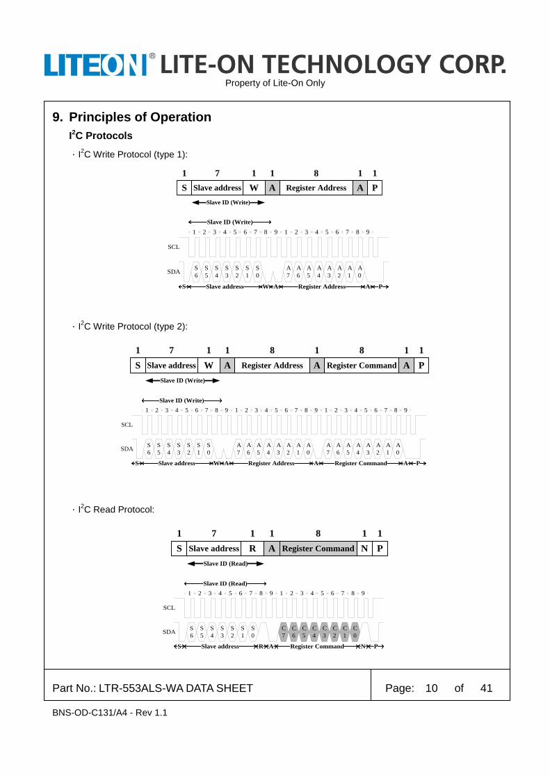
9. Principles of Operation
I2C Protocols
.I2C Write Protocol (type 1):
Slave address W AS Register Address A P
7 1 11 8 1 1
Slave ID (Write)
SCL
1 2 3 4 5 6 7 8 9
SDAS
6
S
5
S
4
S
3
S
2
S
1
S
0
1 2 3 4 5 6 7 8 9
A
7
A
6
A
5
A
4
A
3
A
2
A
1
A
0
Slave address Register AddressA AS PW
Slave ID (Write)
.I2C Write Protocol (type 2):
Slave address W AS Register Address A P
7 1 11 8 1 1
Register Command A
8 1
Slave ID (Write)
SCL
1 2 3 4 5 6 7 8 9
SDAS
6
S
5
S
4
S
3
S
2
S
1
S
0
1 2 3 4 5 6 7 8 9
A
7
A
6
A
5
A
4
A
3
A
2
A
1
A
0
Slave address Register AddressA AS
1 2 3 4 5 6 7 8 9
A
7
A
6
A
5
A
4
A
3
A
2
A
1
A
0
Register Command A PW
Slave ID (Write)
.I2C Read Protocol:
S
1
Slave address R A N
7 1 1 8 1
Register Command P
1
Slave ID (Read)
SCL
1 2 3 4 5 6 7 8 9
SDAS
6
S
5
S
4
S
3
S
2
S
1
S
0
1 2 3 4 5 6 7 8 9
C
7
C
6
C
5
C
4
C
3
C
2
C
1
C
0
Slave address Register CommandA NS PR
Slave ID (Read)

Property of Lite-On Only
Part No.: LTR-553ALS-WA DATA SHEET Page: 11 of 41 BNS-OD-C131/A4 - Rev 1.1
.I2C Read (Combined format) Protocol:
Slave address W AS Register Address A Sr
7 1 11 8 1 1
Slave address R A N
7 1 1 8 1
Register Command P
1
Slave ID (Write) Slave ID (Read)
SCL
1 2 3 4 5 6 7 8 9
SDAS
6
S
5
S
4
S
3
S
2
S
1
S
0
1 2 3 4 5 6 7 8 9
A
7
A
6
A
5
A
4
A
3
A
2
A
1
A
0
Slave address Register AddressA AS SrW
1 2 3 4 5 6 7 8 9
C
7
C
6
C
5
C
4
C
3
C
2
C
1
C
0
Register CommandA N P
1 2 3 4 5 6 7 8 9
S
6
S
5
S
4
S
3
S
2
S
1
S
0
Slave address AR
……
……
……
……
Slave ID (Write) Slave ID (Read)
A Acknowledge (0 for an ACK) N Non-Acknowledge(1 for an NACK)
S Start condition Sr Repeated Start condition
P Stop condition W Write (0 for writing) R Read (1 for read)
Slave-to-master Master-to-Slave

Property of Lite-On Only
Part No.: LTR-553ALS-WA DATA SHEET Page: 12 of 41 BNS-OD-C131/A4 - Rev 1.1
I2C Slave Address
The 7 bits slave address for this sensor is 0x23H. A read/write bit should be appended to the slave
address by the master device to properly communicate with the sensor.
I2C Slave Address
Command
Type
(0x23H) W/R value
Bit7 Bit6 Bit5 Bit4 Bit3 Bit2 Bit1 Bit0
Write 0 1 0 0 0 1 1 0 0x46H
Read 0 1 0 0 0 1 1 1 0x47H

Property of Lite-On Only
Part No.: LTR-553ALS-WA DATA SHEET Page: 13 of 41 BNS-OD-C131/A4 - Rev 1.1
Register Set
Addr R / W Register Name Description Reset Value
0x80 R / W ALS_CONTR ALS operation mode control SW reset 0x00
0x81 R / W PS_CONTR PS operation mode control 0x00
0x82 R / W PS_LED PS LED setting 0x7F
0x83 R / W PS_N_PULSES PS number of pulses 0x01
0x84 R / W PS_MEAS_RATE PS measurement rate in active mode 0x02
0x85 R / W ALS_MEAS_RATE ALS measurement rate in active mode 0x03
0x86 R PART_ID Part Number ID and Revision ID 0x92
0x87 R MANUFAC_ID Manufacturer ID 0x05
0x88 R ALS_DATA_CH1_0 ALS measurement CH1 data, lower byte 0x00
0x89 R ALS_DATA_CH1_1 ALS measurement CH1 data, upper byte 0x00
0x8A R ALS_DATA_CH0_0 ALS measurement CH0 data, lower byte 0x00
0x8B R ALS_DATA_CH0_1 ALS measurement CH0 data, upper byte 0x00
0x8C R ALS_PS_STATUS ALS and PS new data status 0x00
0x8D R PS_DATA_0 PS measurement data, lower byte 0x00
0x8E R PS_DATA_1 PS measurement data, upper byte 0x00
0x8F R / W INTERRUPT Interrupt settings 0x00
0x90 R / W PS_THRES_UP_0 PS interrupt upper threshold, lower byte 0xFF
0x91 R / W PS_THRES_UP_1 PS interrupt upper threshold, upper byte 0x07
0x92 R / W PS_THRES_LOW_0 PS interrupt lower threshold, lower byte 0x00
0x93 R / W PS_THRES_LOW_1 PS interrupt lower threshold, upper byte 0x00
0x94 R/W PS_OFFSET_1 PS offset, upper byte 0x00
0x95 R/W PS_OFFSET_0 PS offset, lower byte 0x00
0x97 R / W ALS_THRES_UP_0 ALS interrupt upper threshold, lower byte 0xFF
0x98 R / W ALS_THRES_UP_1 ALS interrupt upper threshold, upper byte 0xFF
0x99 R / W ALS_THRES_LOW_0 ALS interrupt lower threshold, lower byte 0x00
0x9A R / W ALS_THRES_LOW_1 ALS interrupt lower threshold, upper byte 0x00
0x9E R / W INTERRUPT PERSIST ALS / PS Interrupt persist setting 0x00
Notes:
When reading ALS/PS data registers, read sequence should always be from lower address to higher address (E.g. For
ALS data, Ch1 data should be read first followed by Ch0 data. Read sequence should be 0x88, 0x89, 0x8A, 0x8B.
When 0x8B is read, all four ALS data registers will be populated with new set of data).
When setting of INTERRUPT register (0x8F) is necessary, it should be done before the device is in Active mode.

Property of Lite-On Only
Part No.: LTR-553ALS-WA DATA SHEET Page: 14 of 41 BNS-OD-C131/A4 - Rev 1.1
ALS_CONTR Register (0x80)
The ALS_CONTR register controls the ALS Gain setting, ALS operation modes and software (SW) reset
for the sensor. The ALS sensor can be set to either standby mode or active mode. At either of these modes,
the I2C circuitry is always active. The default mode after power up is standby mode. During standby mode,
there is no ALS measurement performed but I2C communication is allowed to enable read/write to all the
registers.
Field Bits Default Type Description
Reserved 7:5 000 -- -- --
ALS Gain 4:2 000 RW
000 Gain 1X 1 lux to 64k lux (default)
001 Gain 2X 0.5 lux to 32k lux
010 Gain 4X 0.25 lux to 16k lux
011 Gain 8X 0.125 lux to 8k lux
100 Reserved
101 Reserved
110 Gain 48X 0.02 lux to 1.3k lux
111 Gain 96X 0.01 lux to 600 lux
SW reset 1 0 RW
0 Initial start-up procedure is NOT started (default)
1 Initial start-up procedure is started, bit has default value of 0 after start-up
ALS mode 0 0 RW 0 Stand-by mode (default)
1 Active mode
0x80 ALS_CONTR (default = 0x00)
B7 B6 B5 B4 B3 B2 B1 B0
Reserved ALS Gain SW
Reset
ALS
Mode
Property of Lite-On Only
Part No.: LTR-553ALS-WA DATA SHEET Page: 15 of 41 BNS-OD-C131/A4 - Rev 1.1
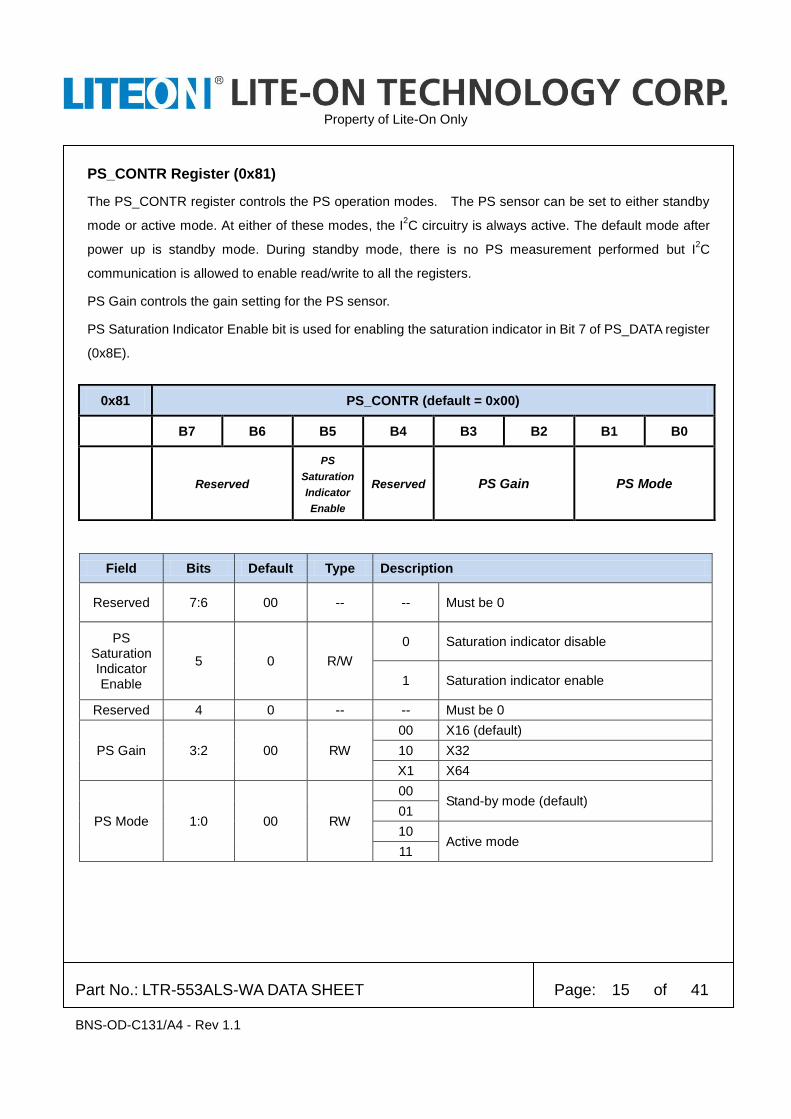
PS_CONTR Register (0x81)
The PS_CONTR register controls the PS operation modes. The PS sensor can be set to either standby
mode or active mode. At either of these modes, the I2C circuitry is always active. The default mode after
power up is standby mode. During standby mode, there is no PS measurement performed but I2C
communication is allowed to enable read/write to all the registers.
PS Gain controls the gain setting for the PS sensor.
PS Saturation Indicator Enable bit is used for enabling the saturation indicator in Bit 7 of PS_DATA register
(0x8E).
Field Bits Default Type Description
Reserved 7:6 00 -- -- Must be 0
PS Saturation Indicator Enable
5 0 R/W
0 Saturation indicator disable
1 Saturation indicator enable
Reserved 4 0 -- -- Must be 0
PS Gain 3:2 00 RW
00 X16 (default)
10 X32
X1 X64
PS Mode 1:0 00 RW
00 Stand-by mode (default)
01
10 Active mode
11
0x81 PS_CONTR (default = 0x00)
B7 B6 B5 B4 B3 B2 B1 B0
Reserved
PS
Saturation
Indicator
Enable
Reserved PS Gain PS Mode
Property of Lite-On Only
Part No.: LTR-553ALS-WA DATA SHEET Page: 16 of 41 BNS-OD-C131/A4 - Rev 1.1
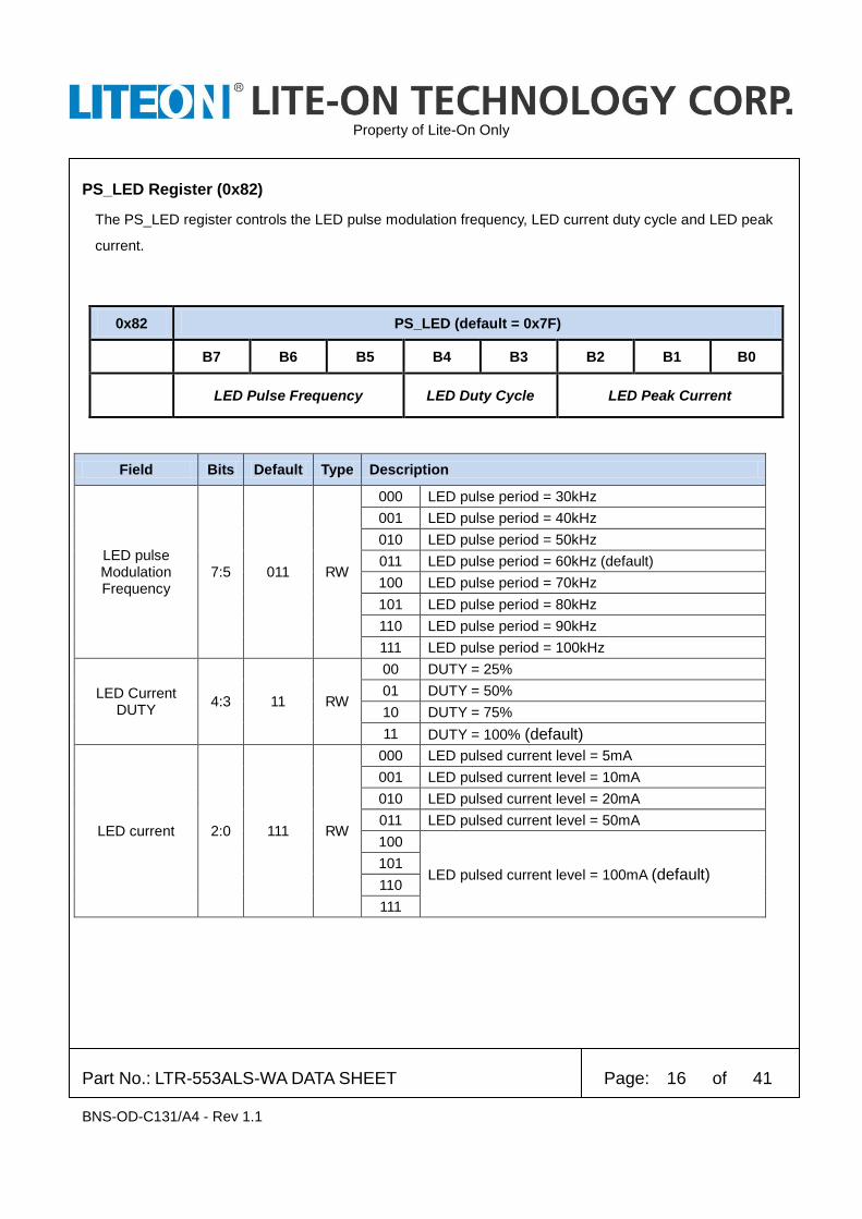
PS_LED Register (0x82)
The PS_LED register controls the LED pulse modulation frequency, LED current duty cycle and LED peak
current.
Field Bits Default Type Description
LED pulse Modulation Frequency
7:5 011 RW
000 LED pulse period = 30kHz
001 LED pulse period = 40kHz
010 LED pulse period = 50kHz
011 LED pulse period = 60kHz (default)
100 LED pulse period = 70kHz
101 LED pulse period = 80kHz
110 LED pulse period = 90kHz
111 LED pulse period = 100kHz
LED Current DUTY
4:3 11 RW
00 DUTY = 25%
01 DUTY = 50%
10 DUTY = 75%
11 DUTY = 100% (default)
LED current 2:0 111 RW
000 LED pulsed current level = 5mA
001 LED pulsed current level = 10mA
010 LED pulsed current level = 20mA
011 LED pulsed current level = 50mA
100
LED pulsed current level = 100mA (default) 101
110
111
0x82 PS_LED (default = 0x7F)
B7 B6 B5 B4 B3 B2 B1 B0
LED Pulse Frequency LED Duty Cycle LED Peak Current

Property of Lite-On Only
Part No.: LTR-553ALS-WA DATA SHEET Page: 17 of 41 BNS-OD-C131/A4 - Rev 1.1
PS_N_Pulses Register (0x83)
The PS_N_Pulses register controls the number of LED pulses to be emitted.
Field Bits Default Type Description
PS number of LED pulses
7:4 0000 RW 0000 (default)
RESERVED (Write only 0000)
3:0 0001 RW
0000 RESERVED
0001 Number of pulses = 1 (default)
0010 Number of pulses = 2
0011 Number of pulses = 3
0100 Number of pulses = 4
0101 Number of pulses = 5
0110 Number of pulses = 6
0111 Number of pulses = 7
1000 Number of pulses = 8
1001 Number of pulses = 9
1010 Number of pulses = 10
1011 Number of pulses = 11
1100 Number of pulses = 12
1101 Number of pulses = 13
1110 Number of pulses = 14
1111 Number of pulses = 15
0x83 PS_N_Pulses (default = 0x01)
B7 B6 B5 B4 B3 B2 B1 B0
Reserved LED Pulse Count
Property of Lite-On Only
Part No.: LTR-553ALS-WA DATA SHEET Page: 18 of 41 BNS-OD-C131/A4 - Rev 1.1
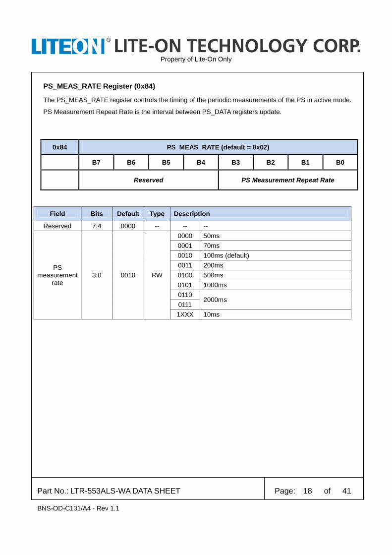
PS_MEAS_RATE Register (0x84)
The PS_MEAS_RATE register controls the timing of the periodic measurements of the PS in active mode.
PS Measurement Repeat Rate is the interval between PS_DATA registers update.
Field Bits Default Type Description
Reserved 7:4 0000 -- -- --
PS measurement
rate 3:0 0010 RW
0000 50ms
0001 70ms
0010 100ms (default)
0011 200ms
0100 500ms
0101 1000ms
0110 2000ms
0111
1XXX 10ms
0x84 PS_MEAS_RATE (default = 0x02)
B7 B6 B5 B4 B3 B2 B1 B0
Reserved PS Measurement Repeat Rate
Property of Lite-On Only
Part No.: LTR-553ALS-WA DATA SHEET Page: 19 of 41 BNS-OD-C131/A4 - Rev 1.1
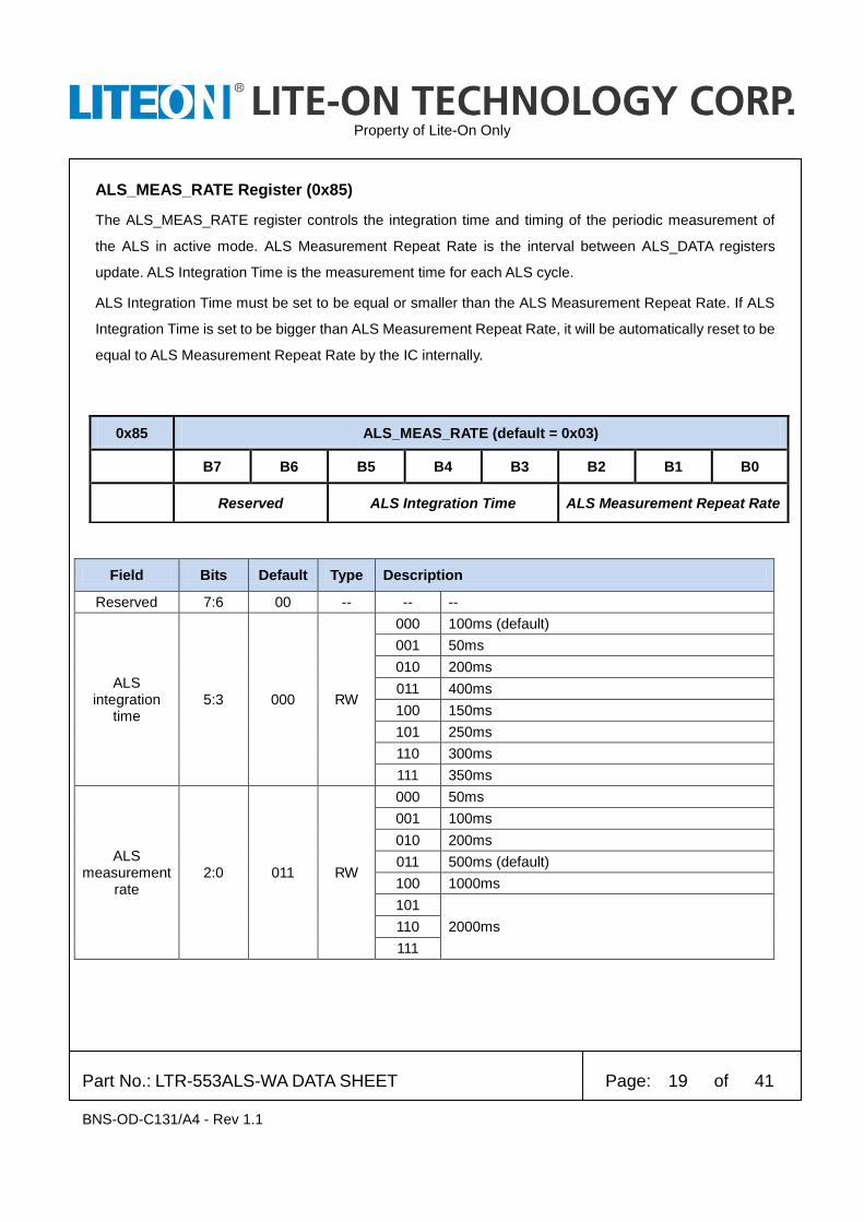
ALS_MEAS_RATE Register (0x85)
The ALS_MEAS_RATE register controls the integration time and timing of the periodic measurement of
the ALS in active mode. ALS Measurement Repeat Rate is the interval between ALS_DATA registers
update. ALS Integration Time is the measurement time for each ALS cycle.
ALS Integration Time must be set to be equal or smaller than the ALS Measurement Repeat Rate. If ALS
Integration Time is set to be bigger than ALS Measurement Repeat Rate, it will be automatically reset to be
equal to ALS Measurement Repeat Rate by the IC internally.
Field Bits Default Type Description
Reserved 7:6 00 -- -- --
ALS integration
time 5:3 000 RW
000 100ms (default)
001 50ms
010 200ms
011 400ms
100 150ms
101 250ms
110 300ms
111 350ms
ALS measurement
rate 2:0 011 RW
000 50ms
001 100ms
010 200ms
011 500ms (default)
100 1000ms
101
2000ms 110
111
0x85 ALS_MEAS_RATE (default = 0x03)
B7 B6 B5 B4 B3 B2 B1 B0
Reserved ALS Integration Time ALS Measurement Repeat Rate
Property of Lite-On Only
Part No.: LTR-553ALS-WA DATA SHEET Page: 20 of 41 BNS-OD-C131/A4 - Rev 1.1
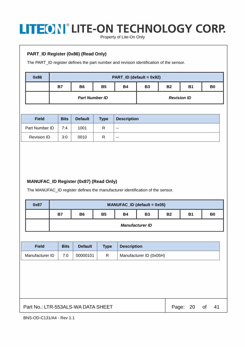
PART_ID Register (0x86) (Read Only)
The PART_ID register defines the part number and revision identification of the sensor.
Field Bits Default Type Description
Part Number ID 7:4 1001 R --
Revision ID 3:0 0010 R --
MANUFAC_ID Register (0x87) (Read Only)
The MANUFAC_ID register defines the manufacturer identification of the sensor.
Field Bits Default Type Description
Manufacturer ID 7:0 00000101 R Manufacturer ID (0x05H)
0x86 PART_ID (default = 0x92)
B7 B6 B5 B4 B3 B2 B1 B0
Part Number ID Revision ID
0x87 MANUFAC_ID (default = 0x05)
B7 B6 B5 B4 B3 B2 B1 B0
Manufacturer ID

Property of Lite-On Only
Part No.: LTR-553ALS-WA DATA SHEET Page: 21 of 41 BNS-OD-C131/A4 - Rev 1.1
ALS_DATA_CH1 Register (0x88 / 0x89) (Read Only)
The ALS_DATA registers should be read as a group, with the lower address read back first (i.e. read 0x88
first, then read 0x89). These two registers should also be read before reading channel-0 data (from registers
0x8A, 0x8B).
When the I2C read operation starts, all four ALS data registers are locked until the I
2C read operation of
register 0x8B is completed. This will ensure that the data in the registers is from the same measurement
even if an additional integration cycle ends during the read operation. New measurement data is stored into
temporary registers and the ALS_DATA registers are updated as soon as there is no on-going I2C read
operation.
The ALS ADC channel-1 data is expressed as a 16-bit data spread over two registers. The
ALS_DATA_CH1_0 and ALS_DATA_CH1_1 registers provide the lower and upper byte respectively.
Field Addr Bits Default Type Description
ALS Data Ch1 Low
0x88 7:0 00000000 R ALS ADC channel 1 lower byte data
ALS Data Ch1 High
0x89 7:0 00000000 R ALS ADC channel 1 upper byte data
0x88 ALS_DATA_CH1_0 (default = 0x00)
B7 B6 B5 B4 B3 B2 B1 B0
ALS Data Ch1 Low
0x89 ALS_DATA_CH1_1 (default = 0x00)
B7 B6 B5 B4 B3 B2 B1 B0
ALS Data Ch1 High

Property of Lite-On Only
Part No.: LTR-553ALS-WA DATA SHEET Page: 22 of 41 BNS-OD-C131/A4 - Rev 1.1
ALS_DATA_CH0 Register (0x8A / 0x8B) (Read Only)
These two registers should be read after reading channel-1 data (from registers 0x88, 0x89). Lower
address register should be read first (i.e read 0x8A first, then read 0x8B). See ALS_DATA_CH1 register
information above.
The ALS ADC channel-0 data is expressed as a 16-bit data spread over two registers. The
ALS_DATA_CH0_0 and ALS_DATA_CH0_1 registers provide the lower and upper byte respectively.
Field Addr Bits Default Type Description
ALS Data Ch0 Low
0x8A 7:0 00000000 R ALS ADC channel 0 lower byte data
ALS Data Ch0 High
0x8B 7:0 00000000 R ALS ADC channel 0 upper byte data
0x8A ALS_DATA_CH0_0 (default = 0x00)
B7 B6 B5 B4 B3 B2 B1 B0
ALS Data Ch0 Low
0x8B ALS_DATA_CH0_1 (default = 0x00)
B7 B6 B5 B4 B3 B2 B1 B0
ALS Data Ch0 High

Property of Lite-On Only
Part No.: LTR-553ALS-WA DATA SHEET Page: 23 of 41 BNS-OD-C131/A4 - Rev 1.1
ALS_PS_STATUS Register (0x8C) (Read Only)
The ALS_PS_STATUS register stores the information about interrupt status and ALS and PS data status.
New data means data has not been read yet. When the measurement is completed and data is written to
the data register, the data status bit will be set to logic 1. When the data register is read, the data status bit
will be set to logic 0.
Interrupt status determines if the ALS and PS interrupt criteria are met. It will check if the ALS or PS
measurement data is outside of the range defined by the upper and lower threshold limits.
ALS Data Valid bit indicates the validity of the ALS data in Ch0 and Ch1.
Field Bits Default Type Description
ALS Data Valid
7 0 R 0 ALS Data is Valid (default)
1 ALS Data is Invalid
ALS Data Gain Range
6:4 000 R
000 ALS measured data in Gain 1X (default)
001 ALS measured data in Gain 2X
010 ALS measured data in Gain 4X
011 ALS measured data in Gain 8X
100 Invalid
101 Invalid
110 ALS measured data in Gain 48X
111 ALS measured data in Gain 96X
ALS interrupt status
3 0 R 0 interrupt signal INACTIVE (default)
1 interrupt signal ACTIVE
ALS data status
2 0 R 0 OLD data (data already read), (default)
1 NEW data (first time data is being read)
PS interrupt status
1 0 R 0 interrupt signal INACTIVE (default)
1 interrupt signal ACTIVE
PS data status
0 0 R 0 OLD data (data already read), (default)
1 NEW data (first time data is being read)
0x8C ALS_PS_STATUS (default = 0x00)
B7 B6 B5 B4 B3 B2 B1 B0
ALS
Data
Valid
ALS Gain
ALS
Interrupt
Status
ALS
Data
Status
PS
Interrupt
Status
PS Data
Status

Property of Lite-On Only
Part No.: LTR-553ALS-WA DATA SHEET Page: 24 of 41 BNS-OD-C131/A4 - Rev 1.1
PS_DATA_0 Register (0x8D / 0x8E) (Read Only)
The PS ADC channel data are expressed as a 11-bit data spread over two registers. The PS_DATA_0 and
PS_DATA_1 registers provide the lower and upper byte respectively. When the I2C read operation starts,
both the registers are locked until the I2C read operation is completed. This will ensure that the data in
the registers is from the same measurement even if an additional integration cycle ends during the read
operation. New measurement data is stored into temporary registers and the PS_DATA registers are
updated as soon as there is no on-going I2C read operation.
PS Saturation Flag is used for monitoring the internal IC saturation. It will be flagged when the IC has
reached saturation and not able to perform any further PS measurement. The PS Saturation Indicator
Enable bit in PS_CONTR Register (0x81) has to be enabled in order to use this feature. If it is not enable,
the flag will always be indicated as 0.
Field Addr Bits Default Type Description
PS Data, Low 0x8D 7:0 00000000 R -- PS ADC lower byte data
PS Saturation Flag 0x8E 7 0 R 0 PS not saturated
1 PS saturated
Reserved 0x8E 6:3 00000 -- -- --
PS Data, High 0x8E 2:0 000 R -- PS ADC upper byte data
0x8D PS_DATA_0 (default = 0x00)
B7 B6 B5 B4 B3 B2 B1 B0
PS Data Low
0x8E PS_DATA_1 (default = 0x00)
B7 B6 B5 B4 B3 B2 B1 B0
PS
Saturation
Flag
Reserved PS Data High
Property of Lite-On Only
Part No.: LTR-553ALS-WA DATA SHEET Page: 25 of 41 BNS-OD-C131/A4 - Rev 1.1
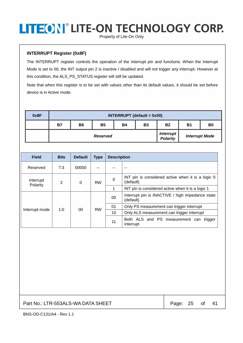
INTERRUPT Register (0x8F)
The INTERRUPT register controls the operation of the interrupt pin and functions. When the Interrupt
Mode is set to 00, the INT output pin 2 is inactive / disabled and will not trigger any interrupt. However at
this condition, the ALS_PS_STATUS register will still be updated.
Note that when this register is to be set with values other than its default values, it should be set before
device is in Active mode.
Field Bits Default Type Description
Reserved 7:3 00000 -- -- --
Interrupt Polarity
2 0 RW 0
INT pin is considered active when it is a logic 0 (default)
1 INT pin is considered active when it is a logic 1
Interrupt mode 1:0 00 RW
00 Interrupt pin is INACTIVE / high impedance state (default)
01 Only PS measurement can trigger interrupt
10 Only ALS measurement can trigger interrupt
11 Both ALS and PS measurement can trigger interrupt
0x8F INTERRUPT (default = 0x00)
B7 B6 B5 B4 B3 B2 B1 B0
Reserved Interrupt
Polarity Interrupt Mode
Property of Lite-On Only
Part No.: LTR-553ALS-WA DATA SHEET Page: 26 of 41 BNS-OD-C131/A4 - Rev 1.1
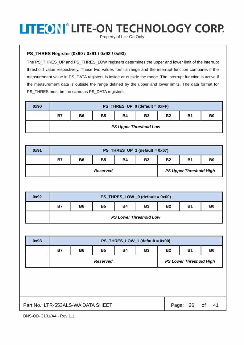
PS_THRES Register (0x90 / 0x91 / 0x92 / 0x93)
The PS_THRES_UP and PS_THRES_LOW registers determines the upper and lower limit of the interrupt
threshold value respectively. These two values form a range and the interrupt function compares if the
measurement value in PS_DATA registers is inside or outside the range. The interrupt function is active if
the measurement data is outside the range defined by the upper and lower limits. The data format for
PS_THRES must be the same as PS_DATA registers.
0x90 PS_THRES_UP_0 (default = 0xFF)
B7 B6 B5 B4 B3 B2 B1 B0
PS Upper Threshold Low
0x91 PS_THRES_UP_1 (default = 0x07)
B7 B6 B5 B4 B3 B2 B1 B0
Reserved PS Upper Threshold High
0x92 PS_THRES_LOW _0 (default = 0x00)
B7 B6 B5 B4 B3 B2 B1 B0
PS Lower Threshold Low
0x93 PS_THRES_LOW_1 (default = 0x00)
B7 B6 B5 B4 B3 B2 B1 B0
Reserved PS Lower Threshold High
Property of Lite-On Only
Part No.: LTR-553ALS-WA DATA SHEET Page: 27 of 41 BNS-OD-C131/A4 - Rev 1.1
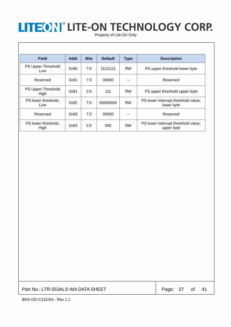
Field Addr Bits Default Type Description
PS Upper Threshold Low
0x90 7:0 11111111 RW PS upper threshold lower byte
Reserved 0x91 7:3 00000 -- Reserved
PS Upper Threshold High
0x91 2:0 111 RW PS upper threshold upper byte
PS lower threshold, Low
0x92 7:0 00000000 RW PS lower interrupt threshold value,
lower byte
Reserved 0x93 7:3 00000 -- Reserved
PS lower threshold, High
0x93 2:0 000 RW PS lower interrupt threshold value,
upper byte

Property of Lite-On Only
Part No.: LTR-553ALS-WA DATA SHEET Page: 28 of 41 BNS-OD-C131/A4 - Rev 1.1
PS_OFFSET Register (0x94 / 0x95)
The PS_OFFSET register defines the offset compensation value for proximity offsets caused by device
variations, optical crosstalk and other environment factors. This value will be used and cancelled from the
original PS raw data such that the data in PS_DATA register (0x8D and 0x8E) are the compensated value.
0x94 PS_OFFSET_1 (default = 0x00)
B7 B6 B5 B4 B3 B2 B1 B0
Reserved PS Offset,
High byte
0x95 PS_OFFSET_0 (default = 0x00)
B7 B6 B5 B4 B3 B2 B1 B0
PS Offset, Low byte
Property of Lite-On Only
Part No.: LTR-553ALS-WA DATA SHEET Page: 29 of 41 BNS-OD-C131/A4 - Rev 1.1
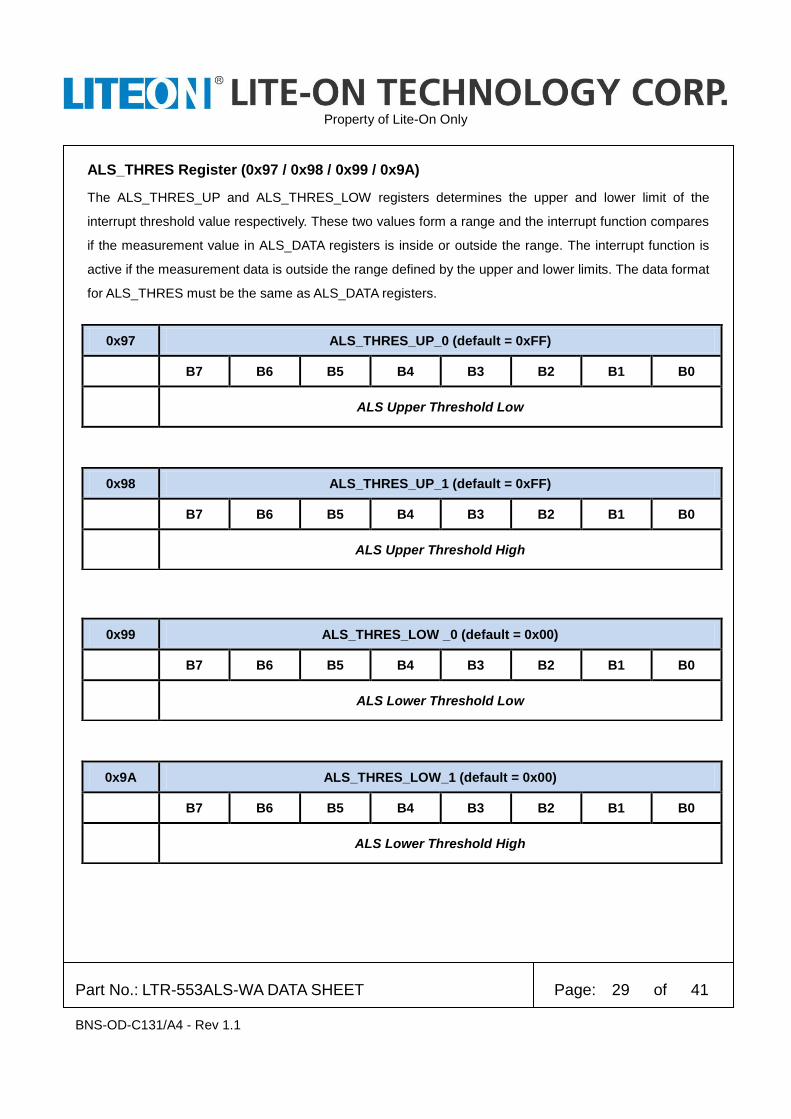
ALS_THRES Register (0x97 / 0x98 / 0x99 / 0x9A)
The ALS_THRES_UP and ALS_THRES_LOW registers determines the upper and lower limit of the
interrupt threshold value respectively. These two values form a range and the interrupt function compares
if the measurement value in ALS_DATA registers is inside or outside the range. The interrupt function is
active if the measurement data is outside the range defined by the upper and lower limits. The data format
for ALS_THRES must be the same as ALS_DATA registers.
0x97 ALS_THRES_UP_0 (default = 0xFF)
B7 B6 B5 B4 B3 B2 B1 B0
ALS Upper Threshold Low
0x98 ALS_THRES_UP_1 (default = 0xFF)
B7 B6 B5 B4 B3 B2 B1 B0
ALS Upper Threshold High
0x99 ALS_THRES_LOW _0 (default = 0x00)
B7 B6 B5 B4 B3 B2 B1 B0
ALS Lower Threshold Low
0x9A ALS_THRES_LOW_1 (default = 0x00)
B7 B6 B5 B4 B3 B2 B1 B0
ALS Lower Threshold High
Property of Lite-On Only
Part No.: LTR-553ALS-WA DATA SHEET Page: 30 of 41 BNS-OD-C131/A4 - Rev 1.1
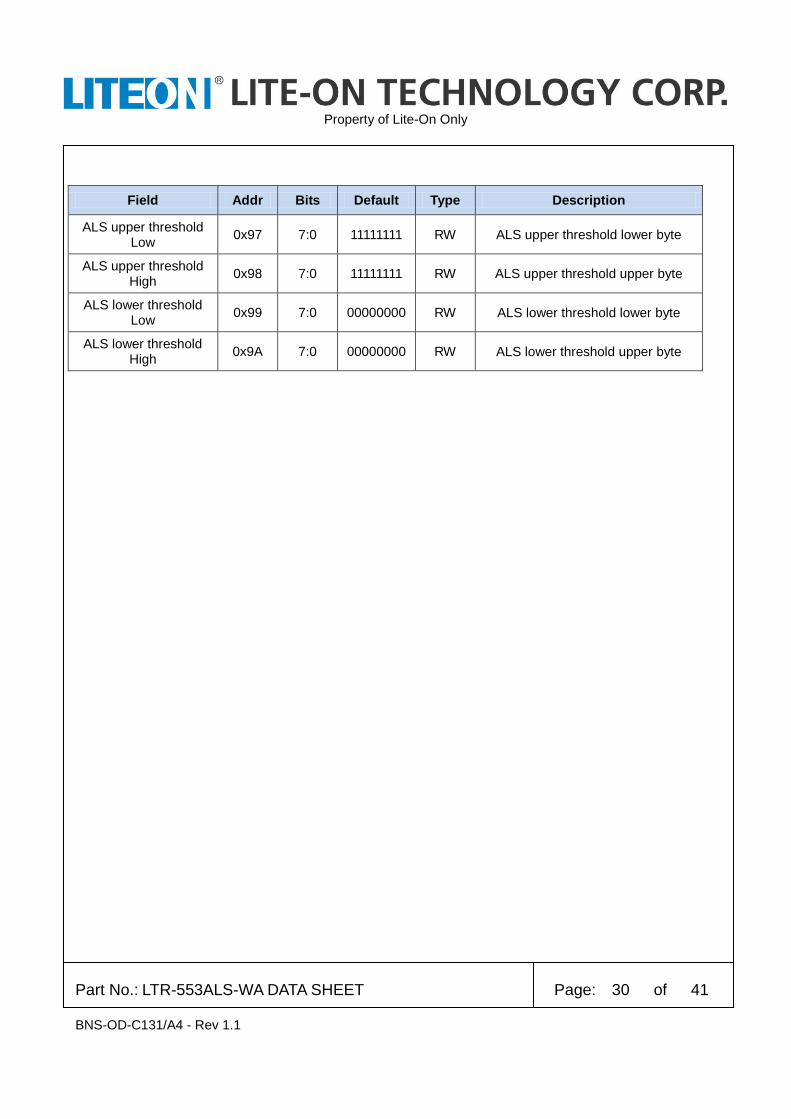
Field Addr Bits Default Type Description
ALS upper threshold Low
0x97 7:0 11111111 RW ALS upper threshold lower byte
ALS upper threshold High
0x98 7:0 11111111 RW ALS upper threshold upper byte
ALS lower threshold Low
0x99 7:0 00000000 RW ALS lower threshold lower byte
ALS lower threshold High
0x9A 7:0 00000000 RW ALS lower threshold upper byte
Property of Lite-On Only
Part No.: LTR-553ALS-WA DATA SHEET Page: 31 of 41 BNS-OD-C131/A4 - Rev 1.1
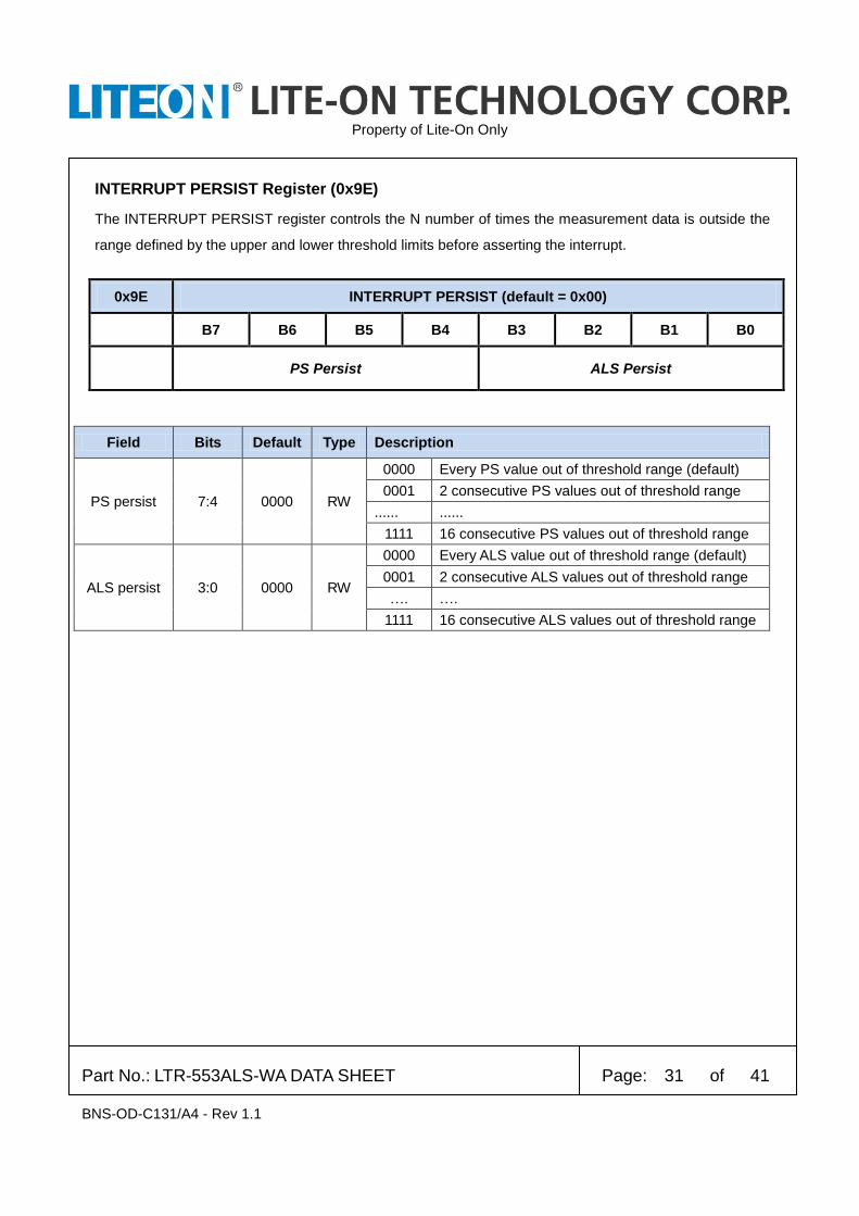
INTERRUPT PERSIST Register (0x9E)
The INTERRUPT PERSIST register controls the N number of times the measurement data is outside the
range defined by the upper and lower threshold limits before asserting the interrupt.
Field Bits Default Type Description
PS persist 7:4 0000 RW
0000 Every PS value out of threshold range (default)
0001 2 consecutive PS values out of threshold range
...... ......
1111 16 consecutive PS values out of threshold range
ALS persist 3:0 0000 RW
0000 Every ALS value out of threshold range (default)
0001 2 consecutive ALS values out of threshold range
…. ….
1111 16 consecutive ALS values out of threshold range
0x9E INTERRUPT PERSIST (default = 0x00)
B7 B6 B5 B4 B3 B2 B1 B0
PS Persist ALS Persist
Property of Lite-On Only
Part No.: LTR-553ALS-WA DATA SHEET Page: 32 of 41 BNS-OD-C131/A4 - Rev 1.1
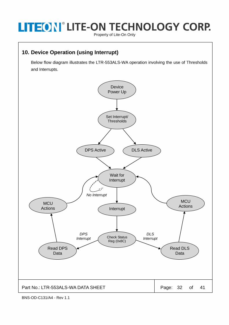
10. Device Operation (using Interrupt)
Below flow diagram illustrates the LTR-553ALS-WA operation involving the use of Thresholds
and Interrupts.
Read DPS Data
Read DLS Data
Device Power Up
DPS Active DLS Active
Interrupt
No Interrupt
DPS Interrupt
DLS Interrupt
MCU Actions
MCU Actions
Wait for Interrupt
Set Interrupt/ Thresholds
Check Status Reg (0x8C)
Property of Lite-On Only
Part No.: LTR-553ALS-WA DATA SHEET Page: 33 of 41 BNS-OD-C131/A4 - Rev 1.1
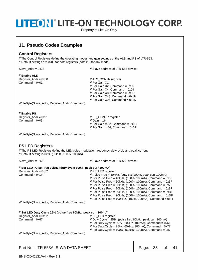
11. Pseudo Codes Examples
Control Registers // The Control Registers define the operating modes and gain settings of the ALS and PS of LTR-553. // Default settings are 0x00 for both registers (both in Standby mode). Slave_Addr = 0x23 // Slave address of LTR-553 device // Enable ALS
Register_Addr = 0x80 // ALS_CONTR register Command = 0x01 // For Gain X1 // For Gain X2, Command = 0x05 // For Gain X4, Command = 0x09 // For Gain X8, Command = 0x0D // For Gain X48, Command = 0x19
// For Gain X96, Command = 0x1D WriteByte(Slave_Addr, Register_Addr, Command) // Enable PS
Register_Addr = 0x81 // PS_CONTR register Command = 0x03 // Gain = 16 // For Gain = 32, Command = 0x0B
// For Gain = 64, Command = 0x0F WriteByte(Slave_Addr, Register_Addr, Command)
PS LED Registers // The PS LED Registers define the LED pulse modulation frequency, duty cycle and peak current. // Default setting is 0x7F (60kHz, 100%, 100mA). Slave_Addr = 0x23 // Slave address of LTR-553 device // Set LED Pulse Freq 30kHz (duty cycle 100%, peak curr 100mA)
Register_Addr = 0x82 // PS_LED register Command = 0x1F // Pulse Freq = 30kHz, (duty cyc 100%, peak curr 100mA)
// For Pulse Freq = 40kHz, (100%, 100mA), Command = 0x3F // For Pulse Freq = 50kHz, (100%, 100mA), Command = 0x5F // For Pulse Freq = 60kHz, (100%, 100mA), Command = 0x7F // For Pulse Freq = 70kHz, (100%, 100mA), Command = 0x9F // For Pulse Freq = 80kHz, (100%, 100mA), Command = 0xBF // For Pulse Freq = 90kHz, (100%, 100mA), Command = 0xDF // For Pulse Freq = 100kHz, (100%, 100mA), Command = 0xFF
WriteByte(Slave_Addr, Register_Addr, Command) // Set LED Duty Cycle 25% (pulse freq 60kHz, peak curr 100mA)
Register_Addr = 0x82 // PS_LED register Command = 0x67 // Duty Cycle = 25%, (pulse freq 60kHz, peak curr 100mA) // For Duty Cycle = 50%, (60kHz, 100mA), Command = 0x6F // For Duty Cycle = 75%, (60kHz, 100mA), Command = 0x77 // For Duty Cycle = 100%, (60kHz, 100mA), Command = 0x7F WriteByte(Slave_Addr, Register_Addr, Command)

Property of Lite-On Only
Part No.: LTR-553ALS-WA DATA SHEET Page: 34 of 41 BNS-OD-C131/A4 - Rev 1.1
// Set LED Peak Current 5mA (pulse freq 60kHz, duty cycle 100%)
Register_Addr = 0x82 // PS_LED register Command = 0x78 // Peak Current = 5mA, (pulse freq 60kHz, duty cyc 100%) // For Peak Current = 10mA, (60kHz, 100%), Command = 0x79 // For Peak Current = 20mA, (60kHz, 100%), Command = 0x7A // For Peak Current = 50mA, (60kHz, 100%), Command = 0x7B WriteByte(Slave_Addr, Register_Addr, Command)
PS Measurement Rate // The PS_MEAS_RATE register controls the PS measurement rate. // Default setting of the register is 0x02 (repeat rate 100ms) Slave_Addr = 0x23 // Slave address of LTR-553 device // Set PS Repeat Rate 50ms
Register_Addr = 0x84 // PS_MEAS_RATE register Command = 0x00 // Meas rate = 50ms // For Meas rate = 500ms, Command = 0x04 WriteByte(Slave_Addr, Register_Addr, Command)
ALS Measurement Rate // The ALS_MEAS_RATE register controls the ALS integration time and measurement rate. // Default setting of the register is 0x03 (integration time 100ms, repeat rate 500ms) Slave_Addr = 0x23 // Slave address of LTR-553 device // Set ALS Integration Time 200ms, Repeat Rate 200ms
Register_Addr = 0x85 // ALS_MEAS_RATE register Command = 0x12 // Int time = 200ms, Meas rate = 200ms // For Int time = 400ms, Meas rate = 500ms, Command = 0x1B WriteByte(Slave_Addr, Register_Addr, Command)
ALS Data Registers (Read Only) // The ALS Data Registers contain the ADC output data for the respective channel. // These registers should be read as a group, with the lower address being read first. Slave_Addr = 0x23 // Slave address of LTR-553 device // Read back ALS_DATA_CH1
Register_Addr = 0x88 // ALS_DATA_CH1 low byte address ReadByte(Slave_Addr, Register_Addr, Data0) Register_Addr = 0x89 // ALS_DATA_CH1 high byte address ReadByte(Slave_Addr, Register_Addr, Data1) // Read back ALS_DATA_CH0
Register_Addr = 0x8A // ALS_DATA_CH0 low byte address ReadByte(Slave_Addr, Register_Addr, Data2) Register_Addr = 0x8B // ALS_DATA_CH0 high byte address ReadByte(Slave_Addr, Register_Addr, Data3) ALS_CH1_ADC_Data = (Data1 << 8) | Data0 // Combining lower and upper bytes to give 16-bit Ch1 data ALS_CH0_ADC_Data = (Data3 << 8) | Data2 // Combining lower and upper bytes to give 16-bit Ch0 data

Property of Lite-On Only
Part No.: LTR-553ALS-WA DATA SHEET Page: 35 of 41 BNS-OD-C131/A4 - Rev 1.1
ALS / PS Status Register (Read Only) // The ALS_PS_STATUS Register contains the information on Interrupt, ALS and PS data availability status. // This register is read only. Slave_Addr = 0x23 // Slave address of LTR-553 device // Read back Register
Register_Addr = 0x8C // ALS_PS_STATUS register address ReadByte(Slave_Addr, Register_Addr, Data) Interrupt_Status = Data & 0x0A // Interrupt_Status = 8(decimal) ALS Interrupt // Interrupt_Status = 2(decimal) PS Interrupt
// Interrupt_Status = 10(decimal) Both Interrupt NewData_Status = Data & 0x05 // NewData_Status = 4(decimal) ALS New Data // NewData_Status = 1(decimal) PS New Data
// NewData_Status = 5(decimal) Both New Data ALS_Data_Valid = Data & 0x80 // ALS_Data_Valid = 0x00 ALS New Data is valid (usable) // ALS_Data_Valid = 0x80 ALS New Data is invalid, discard and wait for new ALS data
PS Data Registers (Read Only) // The PS Data Registers contain the ADC output data. // These registers should be read as a group, with the lower address being read first. Slave_Addr = 0x23 // Slave address of LTR-553 device // Read back PS_DATA registers
Register_Addr = 0x8D // PS_DATA low byte address ReadByte(Slave_Addr, Register_Addr, Data0) Register_Addr = 0x8E // PS_DATA high byte address ReadByte(Slave_Addr, Register_Addr, Data1) PS_ADC_Data = (Data1 << 8) | Data0 // Combining lower and upper bytes to give 16-bit PS data
Interrupt Registers // The Interrupt register controls the operation of the interrupt pins and function. // The default value for this register is 0x08 (Interrupt inactive) Slave_Addr = 0x23 // Slave address of LTR-553 device // Set Interrupt Polarity for Active Low, both ALS and PS trigger
Register_Addr = 0x8F // Interrupt Register address Command = 0x03 // Interrupt is Active Low and both ALS and PS can trigger // For Active High Interrupt, both trigger, Command = 0x07 // For Active High Interrupt, ONLY ALS trigger, Command = 0x06 // For Active High Interrupt, ONLY PS trigger, Command = 0x05 WriteByte(Slave_Addr, Register_Addr, Command)

Property of Lite-On Only
Part No.: LTR-553ALS-WA DATA SHEET Page: 36 of 41 BNS-OD-C131/A4 - Rev 1.1
ALS Threshold Registers // The ALS_THRES_UP and ALS_THRES_LOW registers determines the upper and // lower limit of the interrupt threshold value. // Following example illustrates the setting of the ALS threshold window of // decimal values of 200 (lower threshold) and 1000 (upper threshold) Slave_Addr = 0x23 // Slave address of LTR-553 device // Upper Threshold Setting (decimal 1000)
ALS_Upp_Threshold_Reg_0 = 0x97 // ALS Upper Threshold Low Byte Register address ALS_Upp_Threshold_Reg_1 = 0x98 // ALS Upper Threshold High Byte Register address Data1 = 1000 >> 8 // To convert decimal 1000 into two eight bytes register values Data0 = 1000 & 0xFF WriteByte(Slave_Addr, ALS_Upp_Threshold_Reg_0, Data0) WriteByte(Slave_Addr, ALS_Upp_Threshold_Reg_1, Data1) // Lower Threshold Setting (decimal 200)
ALS_Low_Threshold_Reg_0 = 0x99 // ALS Lower Threshold Low Byte Register address ALS_Low_Threshold_Reg_1 = 0x9A // ALS Lower Threshold High Byte Register address Data1 = 200 >> 8 // To convert decimal 200 into two eight bytes register values Data0 = 200 & 0xFF WriteByte(Slave_Addr, ALS_Low_Threshold_Reg_0, Data0) WriteByte(Slave_Addr, ALS_Low_Threshold_Reg_1, Data1)
PS Threshold Registers // The PS_THRES_UP and PS_THRES_LOW registers determines the upper and // lower limit of the interrupt threshold value. // Following example illustrates the setting of the PS threshold window of // decimal values of 200 (lower threshold) and 1000 (upper threshold) Slave_Addr = 0x23 // Slave address of LTR-553 device // Upper Threshold Setting (decimal 1000)
PS_Upp_Threshold_Reg_0 = 0x90 // PS Upper Threshold Low Byte Register address PS_Upp_Threshold_Reg_1 = 0x91 // PS Upper Threshold High Byte Register address Data1 = 1000 >> 8 // To convert decimal 1000 into two eight bytes register values Data0 = 1000 & 0xFF WriteByte(Slave_Addr, PS_Upp_Threshold_Reg_0, Data0) WriteByte(Slave_Addr, PS_Upp_Threshold_Reg_1, Data1) // Lower Threshold Setting (decimal 200)
PS_Low_Threshold_Reg_0 = 0x92 // PS Lower Threshold Low Byte Register address PS_Low_Threshold_Reg_1 = 0x93 // PS Lower Threshold High Byte Register address Data1 = 200 >> 8 // To convert decimal 200 into two eight bytes register values Data0 = 200 & 0xFF WriteByte(Slave_Addr, PS_Low_Threshold_Reg_0, Data0) WriteByte(Slave_Addr, PS_Low_Threshold_Reg_1, Data1)

Property of Lite-On Only
Part No.: LTR-553ALS-WA DATA SHEET Page: 37 of 41 BNS-OD-C131/A4 - Rev 1.1
12. Recommended Leadfree Reflow Profile
50 100 150 200 250 300t-TIME
(SECONDS)
25
80
120
150
180
200
230
255
0
T -
TE
MP
ER
AT
UR
E (
°C)
R1
R2
R3 R4
R5
217
MAX 260C
60 sec to 90 sec
Above 217 C
P1
HEAT
UP
P2
SOLDER PASTE DRY
P3
SOLDER
REFLOW
P4
COOL DOWN
Process Zone Symbol T Maximum T/time or Duration
Heat Up P1, R1 25C to 150C 3C/s
Solder Paste Dry P2, R2 150C to 200C 100s to 180s
Solder Reflow P3, R3
P3, R4
200C to 260C
260C to 200C
3C/s
-6C/s
Cool Down P4, R5 200C to 25C -6C/s
Time maintained above liquidus point , 217C > 217C 60s to 90s
Peak Temperature 260C -
Time within 5C of actual Peak Temperature > 255C 20s
Time 25C to Peak Temperature 25C to 260C 8mins
It is recommended to perform reflow soldering no more than twice.

Property of Lite-On Only
Part No.: LTR-553ALS-WA DATA SHEET Page: 38 of 41 BNS-OD-C131/A4 - Rev 1.1
13. Moisture Proof Packaging
All LTR-553ALS-WA are shipped in moisture proof package. Once opened, moisture absorption begins.
This part is compliant to JEDEC J-STD-033A Level 3.
Time from Unsealing to Soldering
After removal from the moisture barrier bag, the parts should be stored at the recommended storage
conditions and soldered within seven days. When the moisture barrier bag is opened and the parts are
exposed to the recommended storage conditions for more than seven days, the parts must be baked
before reflow to prevent damage to the parts.
Recommended Storage Conditions
Storage Temperature 10C to 30C
Relative Humidity Below 60% RH
Baking Conditions
Package Temperature Time
In Reels 60C 48 hours
In Bulk 100C 4 hours
Baking should only be done once.

Property of Lite-On Only
Part No.: LTR-553ALS-WA DATA SHEET Page: 39 of 41 BNS-OD-C131/A4 - Rev 1.1
14. Recommended Land Pattern and Metal Stencil Aperture
Recommended Land Pattern
Note:
1. All dimensions are in millimeters
Metal Stencil
for Solder
Paste Printing
Stencil
Aperture
Land
Pattern
PCBA

Property of Lite-On Only
Part No.: LTR-553ALS-WA DATA SHEET Page: 40 of 41 BNS-OD-C131/A4 - Rev 1.1
Recommended Metal Stencil Aperture
It is recommended that the metal stencil used for solder paste printing has a thickness (t) of 0.11mm
(0.004 inches / 4 mils) or 0.127mm (0.005 inches / 5 mils).
The stencil aperture opening is recommended to be 0.72mm x 0.60mm which has the same dimension
as the land pattern. This is to ensure adequate printed solder paste volume and yet no shorting.
Note:
1. All dimensions are in millimeters
2.00
3.63
t
Aperture
Opening

Property of Lite-On Only
Part No.: LTR-553ALS-WA DATA SHEET Page: 41 of 41 BNS-OD-C131/A4 - Rev 1.1
15. Package Dimension for Tape and Reel
Note:
1. All dimensions are in millimeters
Notes:
1. All dimensions are in millimeters (inches)
2. Empty component pockets sealed with top cover tape
3. 13 inch reel - 8000 pieces per reel
4. In accordance with ANSI/EIA 481-1-A-1994 specifications