luceda photonics delivers a silicon … includes a compact model simulator caphe for the optical ......
TRANSCRIPT

A M S D E S I G N & V E R I F I C A T I O N WH
IT
EP
AP
ER
w w w . m e n t o r . c o m
LUCEDA PHOTONICS DELIVERS A SILICON PHOTONICS IC SOLUTION IN TANNER L-EDIT
WIM BOGAERTS, PIETER DUMON, AND MARTIN FIERS, LUCEDA PHOTONICSJEFF MILLER, MENTOR GRAPHICS

w w w. m ento r.co m2
Luceda Photonics Delivers a Silicon Photonics IC Solution in Tanner L-Edit
WHAT IS SILICON PHOTONICS?Silicon photonics is an IC technology where data is transferred using light that is routed on the chip using optical waveguides (Figure 1). Silicon photonics is best known as a method to solve problems with high input/output bandwidth applications. For example, because of ever-growing bandwidth requirements in datacenters, the optical transmit and receive heads are being placed closer and closer to the board and the IC. But, designers also apply this technology to biosensors, medical diagnostics, and environmental monitoring. Regardless of the application, photonic ICs always need integration to electronic circuits and this results in unique challenges. A photonic integrated circuit (PIC) requires key functions:
• Generation of light: using lasers or LEDs either as an external light source, or increasingly, mounted on the IC or even densely integrated with the IC.
• Modulation of light: for switching or for modulating a data stream on the optical carrier. This is accomplished using the density of electrical carriers (electrons and holes) in the core of a waveguide to modulate the phase of the light, or by using electro-absorption to modulate the amplitude of the light.
• Splitting, coupling, and crossing: as light is routed, it is often required to split part of the optical power for monitoring, coupling on and off the IC, or to cross two waveguides.
• Detection of light: using a photodiode that responds to light intensity.
• Wavelength filtering: to filter out specific optical wavelengths or to combine wavelengths together in a single optical waveguide.
• Coupling to the system around the chip: using optical “probe pads” connected to optical fibers, board-level waveguides, or free-space optics.
Figure 1: Components of a PIC arranged in a wavelength-division multiplexer link.

w w w. m ento r.co m3
Luceda Photonics Delivers a Silicon Photonics IC Solution in Tanner L-Edit
THE CHALLENGES OF PHOTONIC IC DESIGNThere is a large gap between what the silicon photonic technology can accomplish and the functionality that designers can actually design and simulate. This gap is due to several key challenges:
1. Physical layout of the PIC. Photonic layout is very different from electronic layout. Photonic devices often contain curvilinear shapes to define smooth waveguide bends. These waveguides need to observe a minimum bend radius in order to avoid propagation losses. Photonic circuit layouts are typically on one layer and routing a complex circuit on a single layer is difficult and often not possible without crossing interconnections. Designers typically want to have full control over every detail of the layout, while at the same time desiring more automation.
2. Physical Verification of the PIC. Photonic designs typically need a special set of design rule checks (DRCs) that might not be easily implemented, due to the curvilinear paths of the waveguides. A big challenge is layout versus schematic (LVS) verification. Extracting functional behavior from a PIC layout is not easy without performing full electromagnetic simulations. Simply checking the interconnections of the design is difficult (Figure 2).
Figure 2: (a) proper connection; (b) physical contact but no angular matching causes loss and reflection; (c) adjacent waveguides might be evanescently coupled without physical contact; (d) waveguides can cross but have little or no coupling.
3. The variability of the fabrication process. The high refractive index contrast of silicon photonics confines light in a submicron waveguide core. But, the effective refractive index depends on the actual geometry of a cross section. Nanometer-level variations on a critical dimension at 200nm have a significant influence on the optical behavior. Not only is it a challenge to efficiently simulate circuits that account for fabrication variability effects, but this variability is one of the reasons for the relative immaturity of the silicon photonics field.
4. The very custom nature of silicon photonic design. Today’s foundry process design kits for silicon photonics typically contain 20-50 basic cells and the maturity level of the kits is not yet very high. In most IC designs taken beyond the first iteration, a large fraction of the basic cells are custom-designed, requiring extensive device simulation (electromagnetic, electro-optical, and thermal behavior). This will remain the case for the foreseeable future. Device technology computer aided design (TCAD) is therefore not only the realm of the fabs, but it is a major job in each design team. Therefore, the device TCAD must be efficiently coupled to the rest of the design flow. In addition, designers typically want keep full control over every detail rather than utilizing full automation.
5. The co-design of complex photonic circuits integrated with electronic circuits. The combined layout of photonic and electronic circuits poses challenges because the nature of the circuits is very different. Routing of the electrical circuitry must not affect the optical behavior and vice versa. A larger challenge is the co-simulation of photonic and electronic circuitry because the light waves are very high frequency

w w w. m ento r.co m4
Luceda Photonics Delivers a Silicon Photonics IC Solution in Tanner L-Edit
electromagnetic waves (300THz). Circuit simulation is typically performed using simulators that use very different formalisms than the SPICE simulators used for electronics.
6. Upscaling the design flow from academic to production grade ICs. A reliable design flow requires integration of photonic functionality addressing the preceding challenges in a production-ready environment. Layout, modeling, and functional test must be integrated not only in a single flow, but in an established electronic design environment that uses paradigms familiar to designers.
THE IPKISS.EDA DESIGN FRAMEWORK SOLUTIONBecause PIC designers need full control of their design framework to ensure that the IC they fabricate exactly matches their design, and they need to conquer the challenges of photonic circuits, Luceda Photonics created the IPKISS.eda design framework (Figure 3). This framework is built on the Tanner L-Edit layout editor which seamlessly interfaces to the Tanner Calibre® One physical verification suite. L-Edit’s rich layout capabilities combined with the IPKISS library of parameterized photonic components and process development kits (PDKs) gives designers the ability to drag and drop photonic components into their layouts and immediately connect them through waveguides, while having full control over cross-section shapes, bends, and trajectories.
Post-layout effects, such as reflections and attenuation caused by waveguide crossings, are taken into account through simulation. IPKISS.eda includes a compact model simulator CAPHE for the optical domain that can handle large optical circuits, including strongly non-linear devices and feedback. The actual layout of the circuit is accounted for by the device models and the tight coupling between the layout and model views. The design flow is enabled with DRC facilities to assure the quality of the design before submitting it to the fab. The designer has fine-grained control over every aspect of the design flow in IPKISS.eda through the Python scripting language.
Figure 3: The IPKISS.eda PIC design flow.
“Photonic IC designers increasingly demand the same first-time-right design experience that electronic IC designers expect. Therefore, we integrated the trusted IPKISS Photonic IC design tool into L-Edit so that photonic IC designers
can improve their design yield by combining expert PIC knowledge into a reliable electronics design flow. We choose to work with the Tanner team because of the excellent match of L-Edit capabilities to PIC design and their
enthusiastic support for bringing innovative solutions to their tools,” stated, Pieter Dumon, Chief Technology Officer of Luceda Photonics.

w w w. m ento r.co m5
Luceda Photonics Delivers a Silicon Photonics IC Solution in Tanner L-Edit
L-Edit supports the OpenAccess database standard managed by Si2, who states: “The OpenAccess Database is the world’s most widely used, open reference database for IC design, with a supporting standard API. It was developed to create authentic interoperability between EDA companies and semiconductor designers and manufacturers. Its adoption has improved design flow efficiency across the industry.”
The L-Edit integration with IPKISS.eda is accomplished using an OpenAccess plugin that translates IPKISS objects into OpenAccess objects. Through this plugin, the IPKISS.eda framework can instantiate parameterized cells (P-Cells) from an OpenAccess database. Designers transparently instantiate IPKISS P-Cells in L-Edit through the OpenAccess API which results in a one-to-one mapping between the cells and their parameters in L-Edit and IPKISS.eda. The framework also encodes the Layer Purpose Pairs in the OpenAccess database, so that they can be read by L-Edit. This plugin uses Si2’s oaScript, which provides an interface between the Python scripting language and the OpenAccess Database.
The IPKISS.eda framework includes custom L-Edit macros to provide photonics-specific functionality to design photonic circuits, such as routing and drawing waveguides. These macros use the L-Edit User-Programmable Interface (UPI) and the OpenAccess database directly. The UPI provides a powerful set of tools for automating, customizing, and extending L-Edit commands and functions. These custom macros are written in Python, so the framework embeds a Python interpreter in L-Edit.
SAMPLE USE CASEThe high-level steps of the solution are best conveyed using a sample use case: the design of a 2x2 optical crossbar switch design (Figure 4) that can scale up to a full NxN cross-connect matrix. There are four grating couplers for connecting the optical signals to fibers and to the bond pads for the electrical steering signals and ground.
Figure 4: A 2x2 cross-connect switch architecture.
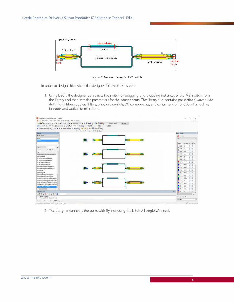
The main building block for the design is a 1x2 thermo-optic Mach-Zehnder Interferometer (MZI) switch (Figure 5). The 1x2 splitter separates the optical signal into the two arms of the MZI. The heater in the arm is steered by electrical signals. The signals in the two arms are coupled into a 2x2 combiner in order to feed the next stage.
w w w. m ento r.co m6
Luceda Photonics Delivers a Silicon Photonics IC Solution in Tanner L-Edit
Figure 5: The thermo-optic MZI switch.
In order to design this switch, the designer follows these steps:
1. Using L-Edit, the designer constructs the switch by dragging and dropping instances of the MZI switch from the library and then sets the parameters for the components. The library also contains pre-defined waveguide definitions, fiber couplers, filters, photonic crystals, I/O components, and containers for functionality such as fan-outs and optical terminations.
2. The designer connects the ports with flylines using the L-Edit All Angle Wire tool.

w w w. m ento r.co m7
Luceda Photonics Delivers a Silicon Photonics IC Solution in Tanner L-Edit
3. Next, the designer generates the waveguides which controls shapes and bends through an automatic routing solution, or the designer can choose to manually route. IPKISS.eda takes care of the proper alignment of optical ports that need to match down to the nanometer grid level.

w w w. m ento r.co m8
Luceda Photonics Delivers a Silicon Photonics IC Solution in Tanner L-Edit
4. Within L-Edit, the designer adjusts the waveguide paths and analyzes or introduces crossings. Because photonic circuits are typically implemented in a single routing layer, the immediate visual feedback on the circuit topology in the layout (for example, unwanted crossings) reduces both the design time and the potential errors. If necessary, the designer manually inserts a crossing component from the library and connects it to the corresponding switches. IPKISS.eda then generates new waveguides.
5. The designer then adds the bond pads and connects them using the L-Edit Orthogonal Wire tool.
6. Using the L-Edit interface to Tanner Calibre One nmDRC™, the designer can easily verify the circuit for DRC violations against the rule deck provided by the foundry and interact with the results browser and the layout. However, the knowledge embedded in IPKISS.eda avoids many of the common DRC violations that typically arise from routing curvilinear shapes.

w w w. m ento r.co m9
Luceda Photonics Delivers a Silicon Photonics IC Solution in Tanner L-Edit
7. For functional verification, the designer can use the CAPHE optical circuit simulator in IPKISS.eda to verify how parameter changes to devices, the connections, or insertion of crossings affect the functional behavior.
The CAPHE simulator builds and simulates optical circuits in frequency or time domain. Post-layout simulations require frequent interplay between the layout editor and the optical simulator and CAPHE has a tight integration with IPKISS. The designer can take advantage of this integration in novel ways. For example, the designer can build layouts that use circuit simulations to design themselves. For instance, the radius of a ring could be calculated using circuit simulations to match a certain optical resonance. Because of this integration, the parametric components can be made very smart and their intelligence is directly accessible from L-Edit. If necessary, IPKISS.eda can dive into the physical domain and launch electromagnetic simulations on individual cells in order to build a device model.
CONCLUSIONThe IPKISS design framework enables a tight integration of the circuit simulation and layout design flow of photonic integrated circuits. Photonic IC designers are very comfortable starting the design at the layout level because design complexity arises from the diversity and complexity of the cells and their interconnection, not the number of cells. Because layout and specific implementation choices have a big impact on the circuit behavior, designers need the fine-grained control provided by IPKISS.eda. The integration of the framework with L-Edit facilitates the definition and reiteration of the connectivity of the physical layout, analyzing DRC results, and performing efficient post-layout functional verification all within the same production-ready design environment.

TECH14620-wMGC 8-16
©2016 Mentor Graphics Corporation, all rights reserved. This document contains information that is proprietary to Mentor Graphics Corporation and may be duplicated in whole or in part by the original recipient for internal business purposes only, provided that this entire notice appears in all copies. In accepting this document, the recipient agrees to make every reasonable effort to prevent unauthorized use of this information. All trademarks mentioned in this document are the trademarks of their respective owners.
F o r t h e l a t e s t p r o d u c t i n f o r m a t i o n , c a l l u s o r v i s i t : w w w . m e n t o r . c o m
Luceda Photonics Delivers a Silicon Photonics IC Solution in Tanner L-Edit
ABOUT LUCEDA PHOTONICS
Luceda Photonics wants photonic IC engineers to enjoy the same first-time-right design experience as electronic IC designers. Luceda Photonics’ tools and services are rooted in over 50 years of experience in photonic integrated circuit (PIC) design.
The team’s expertise in the development of process design kits (PDK) and the design and validation of photonic integrated circuits is used by several research institutes and industrial R&D teams worldwide.