lui: twisted pair tutorial - using ftt-10a...
TRANSCRIPT
Slide 1
Twisted Pair Tutorial:Using FTT-10A Transceivers
• Introduction
• General PCB Layout Considerations
• Avoiding Magnetic Field Interference
• Physical Layer Repeaters
• Using Category 5 Wire
• General Network Cable Considerations
• IEC 1000-4-6 Conducted RF Susceptibility
• Some Troubleshooting Tips

Slide 2
Introduction• The FTT-10A Transceiver is Echelon’s most popular transceiver
≥ 90% of new design wins are with the FTT-10A transceiver
• Echelon offers free design reviews for products with EchelonOEM content (like Echelon transceivers, modules, etc.)
– All customer documentation is kept confidential, and theinformation can be returned to the customer or destroyed afterthe review is complete
– The best time for a design review on a new product is whenyou have a schematic, BOM and preliminary PCB layout
– Contact your sales person, FAE, or Echelon TechnicalSupport for details

Slide 3
FTT-10A Node Design Reviews:Most Frequently-Made Errors
• Frequent errors in PCB floorplan & layout:– No star ground configuration, and no explicit ESD exit path
– Insufficient grounding and decoupling of the Neuron chip & memory circuit
– The transceiver’s ground is too far from the center of the star ground and thechassis ground connection
– Logic traces are run through the “ESD Keepout” area of the transceiver
• Frequent schematic errors:– The LVI circuit is incorrect, or the wrong LVI part is shown
• The FTT-10A transceiver does not require an LVI, but the Neuron chip ormemory circuit may
• The LVI circuit must be open-collector (many LVIs are not)
– The memory interface circuit is incorrect or too slow• See Echelon’s Neuron 3150 Chip External Memory Interface bulletin
Slide 4
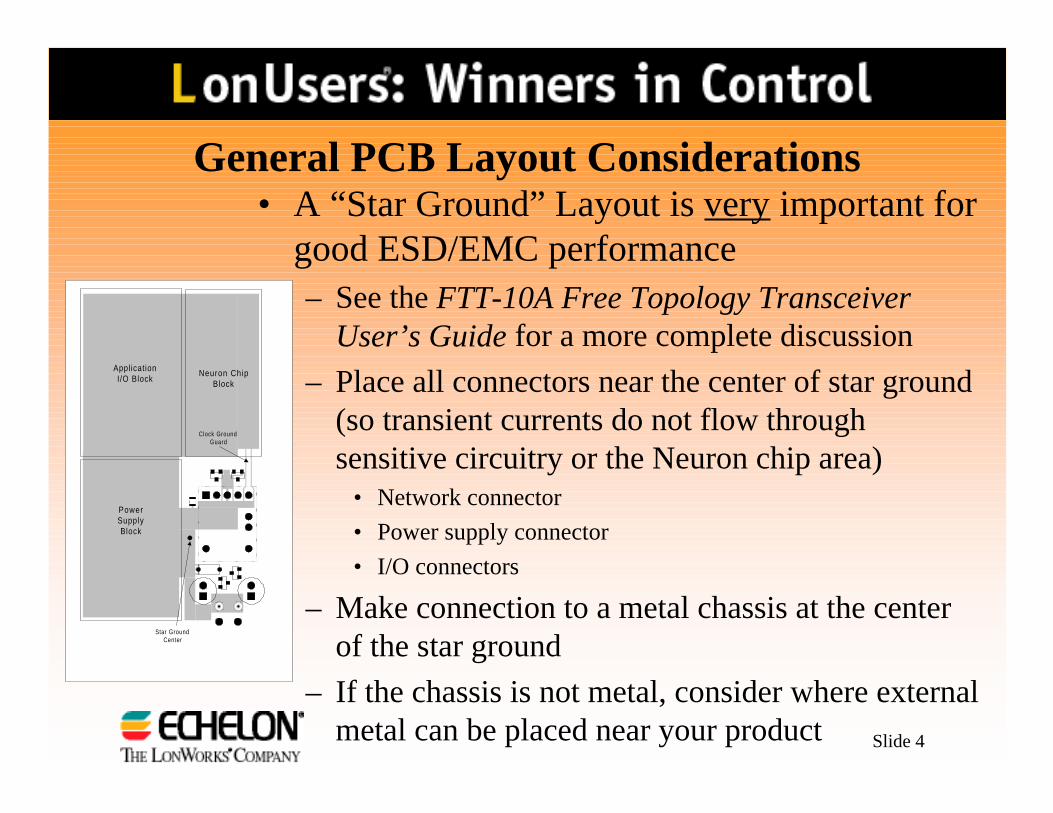
General PCB Layout Considerations
Star GroundCenter
ApplicationI/O Block
PowerSupplyBlock
Neuron ChipBlock
Clock GroundGuard
• A “Star Ground” Layout is very important forgood ESD/EMC performance– See the FTT-10A Free Topology Transceiver
User’s Guide for a more complete discussion
– Place all connectors near the center of star ground(so transient currents do not flow throughsensitive circuitry or the Neuron chip area)
• Network connector
• Power supply connector
• I/O connectors
– Make connection to a metal chassis at the centerof the star ground
– If the chassis is not metal, consider where externalmetal can be placed near your product

Slide 5
General PCB Layout Considerations
C P 0
C P 1
CLK2
C P 2C P 3C P 4
Neuron Chip(Part ial)
+ 5 V
FTT-10A
C 1D 2
+ 5 V
D 1
N E T 1
N E T 2
See Text
C 3
C 4
C 2
PCB SparkGaps
D 3
D 4R X D N E T _ A
N E T _ B
V C C
T1T2
G N D
T X D
C L K
• Chassis and logic grounds canbe separate or connected– Primary ESD energy is diverted
through the spark gaps and C2, soa direct return path to chassis isvery important
– Secondary ESD energy isclamped by D1-D2 and C1, so adirect return to chassis from thetransceiver ground is important
– If logic ground and chassis areseparate, connect them with acapacitor at star center (~ 0.01uF)
Slide 6
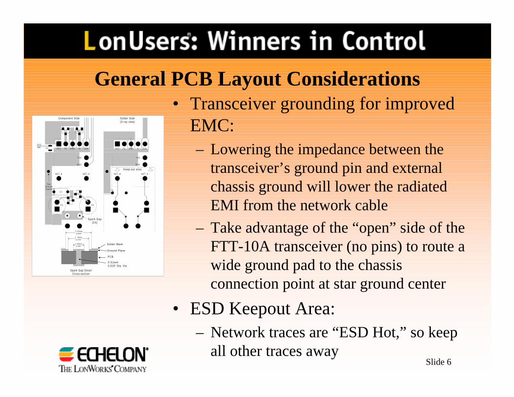
General PCB Layout Considerations• Transceiver grounding for improved
EMC:– Lowering the impedance between the
transceiver’s ground pin and externalchassis ground will lower the radiatedEMI from the network cable
– Take advantage of the “open” side of theFTT-10A transceiver (no pins) to route awide ground pad to the chassisconnection point at star ground center
• ESD Keepout Area:– Network traces are “ESD Hot,” so keep
all other traces away
V C C T 2 T 1G N D C L K
T X D
R X D
N E T _ AN E T _ B
V C C T 2 T1G N D C LK
T X D
R X D
N E T _ AN E T _ B
Component S ide Solder Side(X-ray view)
Keep-out area
C 1
C 3 C 4
D 1 D 2
D 3
StarG r o u n dCen te r
C 2
D 4
Spark Gap(2X)
Solder Mask
Ground P lane
P C B
0 . 5 1 m m0.019" Dia. Via
2 . 3 0 m m0.090"
1 . 7 8 m m0.070"
1 . 0 0 m m0.040"
Spark Gap Detai lCross-sect ion
V C CNet
Slide 7
General PCB Layout Considerations• The order of trace layout for a 2-layer PCB should be:
– Place a full ground plane on the solder side of the PCB
– Route the fast digital traces on the component side of the PCB
– Route the rest of the traces, preferably on the component side
– Pour ground pads in any open areas, and connect them to themain ground plane with vias
• Keep the leakage capacitance low from digital traces tochassis metal (or external metal outside the product)– This reduces the RF noise on your logic ground
• Consider using “VHC” logic in memory interface circuits– VHC has AC speed, and slower edges for better EMC
Slide 8
Avoiding Magnetic Field Interference• All transformer-based transceivers are vulnerable to stray
magnetic field noise
• The FTT-10A transceiver is least sensitive to vertical fields, andmost sensitive to horizontal fields
• (The old FTT-10 transceiver was the opposite: it was mostsensitive to vertical fields)
• To avoid interference with FTT-10A communication:
– Quiet the sources of magnetic field noise
– Keep any remaining stray fields vertical at the PCB surface
• Common-mode voltage noise on logic ground can sometimes“masquerade” as magnetic field interference

Slide 9
Sources of Magnetic Field Noise:DC-DC Converter Magnetic Components
Horizonta l Ax ia l -Lead S lug Induc tor(S ide V iew)
Ver t i ca l Rad ia l -Lead S lug Induc tor(S ide V iew)
St rayB-F ie ld
S t rayB-F ie ld
P C B
P C B
• Slug Style Inductors– Horizontal axial-lead slug
inductors generate horizontalstray fields at the PCB surface
– Vertical radial-lead sluginductors generate vertical strayfields at the PCB surface
• Radial-lead slug inductors withbuilt-in magnetic shielding areavailable (for example: Taiyo-Yuden LHFP type, or TDK FStype)
Slide 10
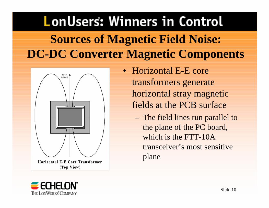
Sources of Magnetic Field Noise:DC-DC Converter Magnetic Components
Horizonta l E-E Core Transformer(Top V iew)
StrayB-Field
• Horizontal E-E coretransformers generatehorizontal stray magneticfields at the PCB surface– The field lines run parallel to
the plane of the PC board,which is the FTT-10Atransceiver’s most sensitiveplane
Slide 11
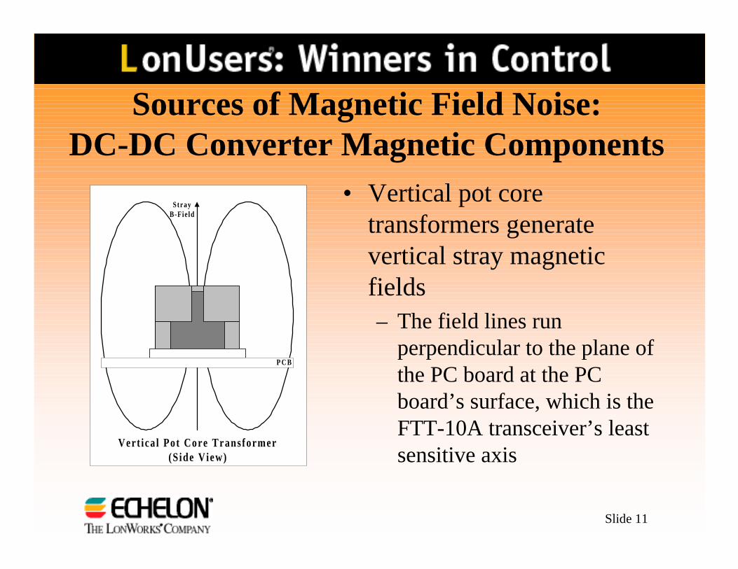
Sources of Magnetic Field Noise:DC-DC Converter Magnetic Components
Vert ica l Pot Core Transformer(Side View)
StrayB-Fie ld
P C B
• Vertical pot coretransformers generatevertical stray magneticfields– The field lines run
perpendicular to the plane ofthe PC board at the PCboard’s surface, which is theFTT-10A transceiver’s leastsensitive axis
Slide 12
Avoiding Magnetic Field Interference• In general, keep the source of stray magnetic field noise away from
the transceiver, quiet it down as much as possible, and keep anyremaining stray fields vertical as they pass through the PCB
• To quiet a non-isolated “buck” or “boost” DC-DC, use a shieldedvertical radial-lead slug (i.e: Taiyo-Yuden LHFP type, or TDK FS type)
• To quiet an isolated transformer-based DC-DC:– Best: Use a bifilar, full circumference-wound toroidal transformer
– Good: Use a vertical pot-core transformer
– Otherwise: Use a shield fence (made from 1mm thick steel), or an externalshorted turn (made from copper tape) with an E-E core transformer
• For harsh magnetic field environments, use a 5-sided steel shield ontop of the FTT-10A transceiver
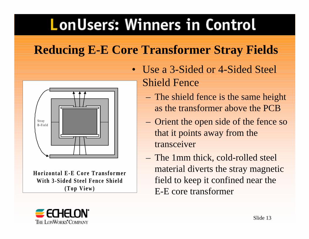
Slide 13
Reducing E-E Core Transformer Stray Fields
Hor izonta l E-E Core TransformerWith 3-Sided Steel Fence Shie ld
(Top V iew)
StrayB-F ie ld
• Use a 3-Sided or 4-Sided SteelShield Fence– The shield fence is the same height
as the transformer above the PCB
– Orient the open side of the fence sothat it points away from thetransceiver
– The 1mm thick, cold-rolled steelmaterial diverts the stray magneticfield to keep it confined near theE-E core transformer
Slide 14
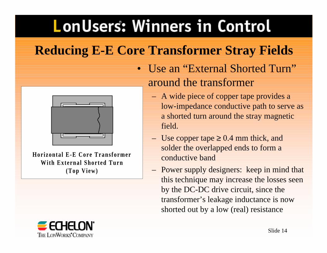
Reducing E-E Core Transformer Stray Fields
Hor izonta l E-E Core TransformerWi th Externa l Shor ted Turn
(Top V iew)
• Use an “External Shorted Turn”around the transformer– A wide piece of copper tape provides a
low-impedance conductive path to serve asa shorted turn around the stray magneticfield.
– Use copper tape ≥ 0.4 mm thick, andsolder the overlapped ends to form aconductive band
– Power supply designers: keep in mind thatthis technique may increase the losses seenby the DC-DC drive circuit, since thetransformer’s leakage inductance is nowshorted out by a low (real) resistance

Slide 15
Shielding the FTT-10A Transceiver
5-Sided Shie ld for Harsh Magnet icF ie ld Env i ronments (Top V iew)
F T T - 1 0 ATransce iver
Fold Cornersand Place Shie ld
On Top o fTransceiver
1mm Thick Stee l Sheet
• For harsh magnetic field environments, a5-sided steel shield can be placed on topof the transceiver:– Use 1mm thick, cold rolled steel to divert the
magnetic field around the transceiver’sinternal volume as much as possible
– This shield technique works best if the sourceof the stray field is above the transceiver, andthe stray magnetic field lines are verticalwhen they pierce the plane of the PCB at thetransceiver (so that the 5-sided shield divertsthe field around the transceiver volume)
Slide 16
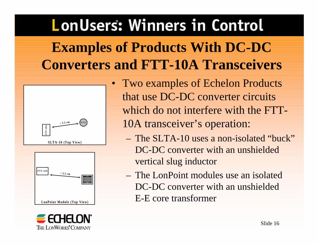
Examples of Products With DC-DCConverters and FTT-10A Transceivers
SLTA-10 (Top V iew)
LonPo in t Modu le (Top V iew)
F T T - 1 0 A
S L U G
FT
T-1
0A
~ 3.5 cm
~ 3.5 cm
• Two examples of Echelon Productsthat use DC-DC converter circuitswhich do not interfere with the FTT-10A transceiver’s operation:– The SLTA-10 uses a non-isolated “buck”
DC-DC converter with an unshieldedvertical slug inductor
– The LonPoint modules use an isolatedDC-DC converter with an unshieldedE-E core transformer

Slide 17
Testing For Magnetic Field Interference• A node may have enough local magnetic field interference to
cause communication problems in a full-size network, but notenough to cause obvious problems in a small network
• A differential probe can be used to check for interference at theFTT-10A receiver’s input pins (T1 and T2)– Typical differential probes are the HP1141 and Tektronix P6046.
– Place both tips of the differential probe on T1, and check that nodifferential voltage is measured. This verifies that the common-moderejection of the probe is sufficient for this measurement.
– Place the differential probe across T1-T2. When there is no incomingnetwork signal, there should be < 10mVpp of noise. If there is
> 10mVpp of noise, then the DC-DC or some other source isinterfering with the full range of performance of the FTT-10Atransceiver.
Slide 18
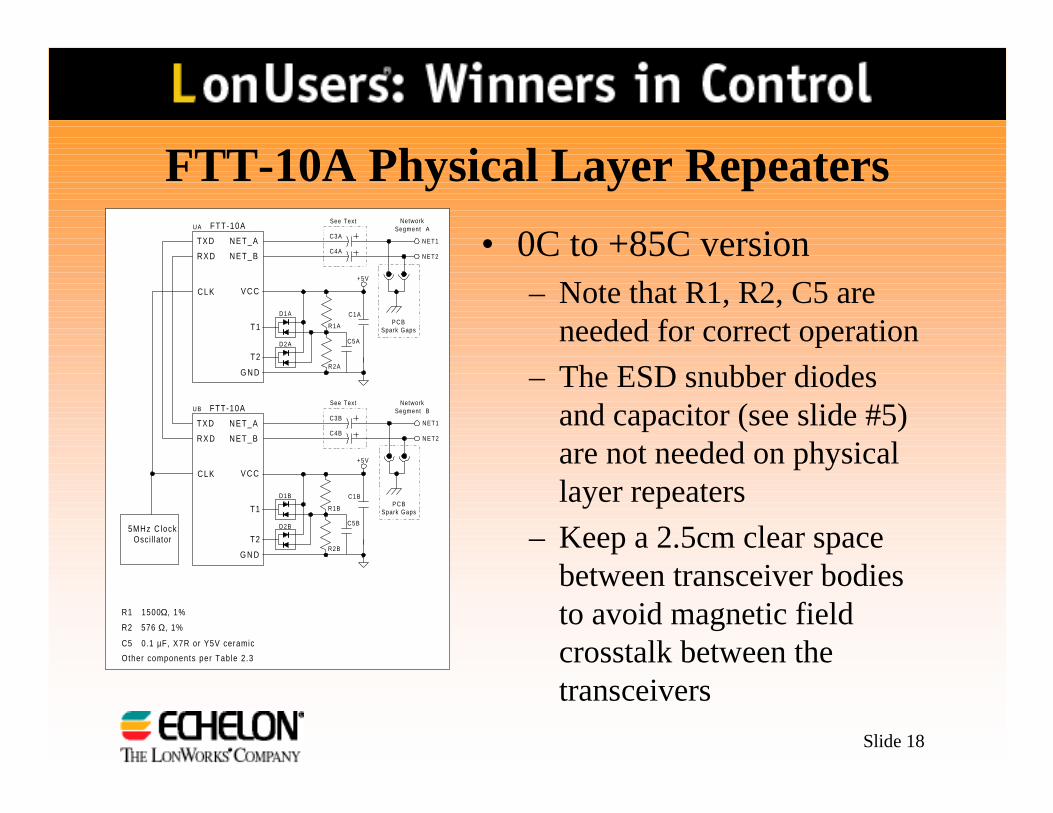
FTT-10A Physical Layer Repeaters
NET1
NET2
PCBSpark Gaps
+5V
5MHz ClockOsci l lator
See Text
C4B
C3BNET_A
NET_B
V C C
T1
T2
G N D
TXD
R X D
C L K
FTT-10A
C1B
D2B
D1B
C5B
R1B
R2B
R1 1500Ω, 1%
R2 576 Ω, 1%
C5 0.1 µF, X7R or Y5V ceramic
Other components per Table 2.3
NET_A
NET_B
V C C
T1
T2
G N D
TXD
R X D
C L K
FTT-10A
+5V
C1A
See Text
C4A
C3A
D2A
D1A
C5A
R1A
R2A
NET1
NET2
PCBSpark Gaps
UA
UBNetwork
Segment B
NetworkSegment A
• 0C to +85C version– Note that R1, R2, C5 are
needed for correct operation
– The ESD snubber diodesand capacitor (see slide #5)are not needed on physicallayer repeaters
– Keep a 2.5cm clear spacebetween transceiver bodiesto avoid magnetic fieldcrosstalk between thetransceivers
Slide 19
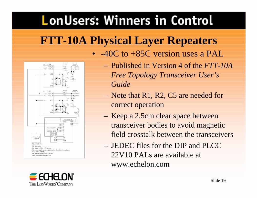
FTT-10A Physical Layer Repeaters
5MHz ClockOscillator
U A
U B
N E T _ A
N E T _ B
V C C
T1
T2
G N D
T X D
R X D
C L K
FTT-10A
+ 5 V
C 1 A
See Text
C 4 A
C 3 A
D 2 A
D 1 A
C 5 A
R 1 A
R 2 A
N E T 1
N E T 2
P C BSpark Gaps
N E T _ A
N E T _ B
V C C
T1
T2
G N D
T X D
R X D
C L K
FTT-10A
+ 5 V
C 1 B
See Text
C 4 B
C 3 B
D 2 B
D 1 B
C 5 B
R 1 B
R 2 B
N E T 1
N E T 2
P C BSpark Gaps
R1 1500Ω, 1%
R2 576 Ω, 1%
C5 0.1 µF, X7R or Y5V ceramic
Other components per Table 2.3
Q6Q7
Q10Q11Q12
> C L KR S T
I0/CLKI1I2I3I4I5I6I7
I8I9I10I11I/O9
R X D A
R X D B
R X D C
R X D D
R X D E
R X D F
I/O0I/O6I/O8
PAL 22V10-25
74HCT4020
Inputs f rom up to fouradd i t iona l FTT-10A
transce ivers (groundany unused inpu ts )
Add power supply bypass capacitors (not shown) next to oscil lator,74HCT4020 and PAL
+ 5 V
2.2k,5 %
N e t w o r kS e g m e n t A
N e t w o r kS e g m e n t B
PAL requires programming: see text
• -40C to +85C version uses a PAL– Published in Version 4 of the FTT-10A
Free Topology Transceiver User’sGuide
– Note that R1, R2, C5 are needed forcorrect operation
– Keep a 2.5cm clear space betweentransceiver bodies to avoid magneticfield crosstalk between the transceivers
– JEDEC files for the DIP and PLCC22V10 PALs are available atwww.echelon.com

Slide 20
Using Category 5 Wire With FTT-10ATransceivers
Table 4.2 Doubly-Terminated Bus Topology Specifications
Maximum bus length Units
Belden 85102 2700 meters
Belden 8471 2700
Level IV, 22AWG 1400
JY (St) Y 2x2x0.8 900
TIA Category 5 900
A doubly-terminated bus may have stubs of up to 3 meters from thebus to each node.
Table 4.3 Free Topology Specifications
Maximumnode-to-nodedistance
Maximum totalwire length
Units
Belden 85102 500 500 meters
Belden 8471 400 500
Level IV, 22AWG 400 500
JY (St) Y 2x2x0.8 320 500
TIA Category 5 250 450
• Version 4 of the FTT-10A FreeTopology Transceiver User’sGuide includes specificationsfor Category 5 wire
– “10/100Base-T” cable
– 24AWG wire
Slide 21
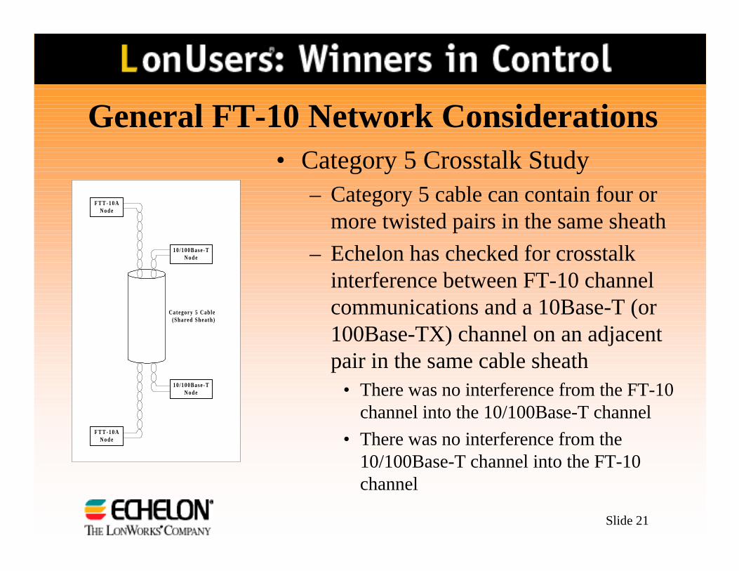
General FT-10 Network Considerations
Category 5 Cable(Shared Sheath)
F T T - 1 0 ANode
10/100Base-TNode
10/100Base-TNode
F T T - 1 0 ANode
• Category 5 Crosstalk Study– Category 5 cable can contain four or
more twisted pairs in the same sheath
– Echelon has checked for crosstalkinterference between FT-10 channelcommunications and a 10Base-T (or100Base-TX) channel on an adjacentpair in the same cable sheath
• There was no interference from the FT-10channel into the 10/100Base-T channel
• There was no interference from the10/100Base-T channel into the FT-10channel
Slide 22
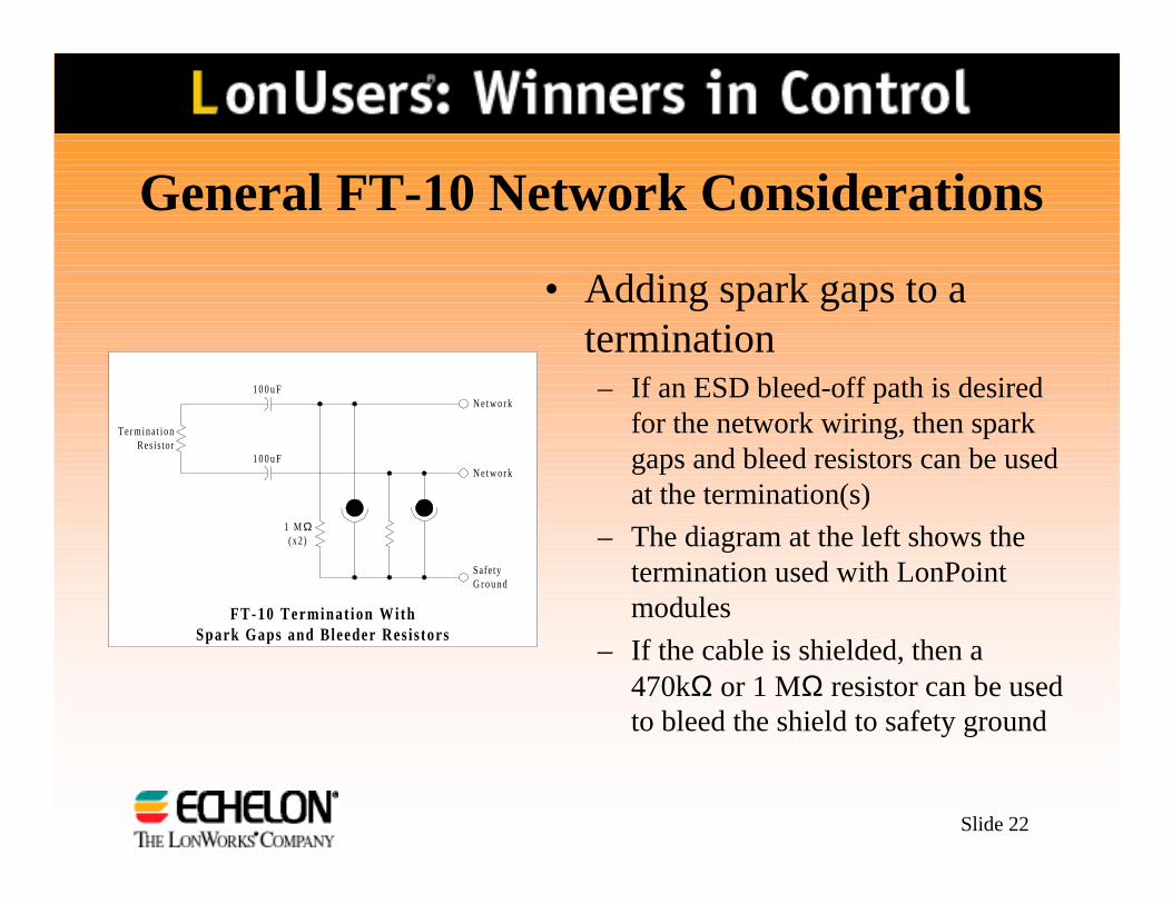
General FT-10 Network Considerations
FT-10 Terminat ion Wi thSpark Gaps and Bleeder Resis tors
Termina t ionResis tor
1 MΩ(x2)
1 0 0 u F
1 0 0 u FNe two rk
Ne two rk
SafetyG r o u n d
• Adding spark gaps to atermination– If an ESD bleed-off path is desired
for the network wiring, then sparkgaps and bleed resistors can be usedat the termination(s)
– The diagram at the left shows thetermination used with LonPointmodules
– If the cable is shielded, then a470kΩ or 1 MΩ resistor can be usedto bleed the shield to safety ground
Slide 23
IEC 1000-4-6 Conducted RF Susceptibility• IEC 1000-4-6 is the upcoming test standard for Conducted RF Susceptibility,
and it will increasingly become a test that is performed on products that use theFTT-10A transceiver
• Several of Echelon’s products have passed IEC 1000-4-6 (they each use acommon-mode choke in the network connection):
– The LonPoint Modules passed Level 3 (10V/m)• They use the muRata PLM250S30T1 SMT common-mode choke
– The SLTA-10 passed Level 2 (3V/m)• It uses the muRata PLT1R53C common-mode choke
– The PCLTA-10 passed Level 2 (3V/m)• It uses the muRata PLT1R53C common-mode choke
• Echelon is conducting more tests on FTT-10A nodes to determine layoutguidelines for passing IEC 1000-4-6, including whether some nodes can passwithout the use of beads or common-mode chokes in their network connection

Slide 24
Some Troubleshooting Tips• A presentation from the 1996 LonUsers
Convention in France is available:Troubleshooting LONWORKS Devices andTwisted Pair Networks– It is available from www.echelon.com (look for
Troubl2.pdf), and from Echelon TechnicalSupport