ma3125ma3126 05c local temperature sensors 05c local temperature sensors 7 block diagram i2c block...
TRANSCRIPT

MAX31725/MAX31726
±0.5°C Local Temperature Sensors
General Description
The MAX31725/MAX31726 temperature sensors accurately measure temperature and provide an overtemperature alarm/interrupt/shutdown output. These devices convert the temperature measurements to digital form using a high-resolution, sigma-delta, analog-to-digital converter (ADC). Accuracy is Q0.5NC from -40NC to +105NC. Communication is through an I2C-compatible 2-wire serial interface.
The I2C serial interface accepts standard write byte, read byte, send byte, and receive byte commands to read the temperature data and configure the behavior of the open-drain overtemperature shutdown output.
The MAX31725 features three address select lines with a total of 32 available addresses. The MAX31726 features two address select lines with a total of 16 available addresses and a RESET input. The sensors have a 2.5V to 3.7V supply voltage range, low 600FA supply current, and a lockup-protected I2C-compatible interface that make them ideal for a wide range of applications, including PCs, electronic test equipment, and office electronics.
Both devices are available in an 8-pin TDFN package and operate over the -55NC to +150NC temperature range.
Benefits and Features
S High Accuracy and Low-Voltage Operation Aids Designers in Meeting Error and Power Budgets ±0.5°C Accuracy from -40°C to +105°C 16-Bit (0.00390625°C) Temperature Resolution 2.5V to 3.7V Supply Voltage Range
S One-Shot and Shutdown Modes Help Reduce Power Usage 925μA (max) Operating Supply Current
S Extended Temperature Range Enables Measurements in High Temperature Systems (Measures Up to +150°C)
S Digital Functions Make Integration Easier into Any System Selectable Timeout Prevents Bus Lockup (Default Enabled for MAX31725; Default Disabled for MAX31726) Separate Open-Drain OS Output Operates as Interrupt or Comparator/Thermostat Output RESET Input (MAX31726)
Applications
Servers
Networking
Telecom
Industrial
Typical Application Circuits
19-6477; Rev 2; 12/14
Ordering Information appears at end of data sheet.
For related parts and recommended products to use with this part, refer to: www.maximintegrated.com/MAX31725.related
MAX31725
VDD0.1µF
+2.5V TO +3.7V
4.7kΩ
A0
A1
A2
SDATO I2C
MASTERSCL
OS
GND
MAX31726
VDD0.1µF
+2.5V TO +3.7V
4.7kΩ
A0
A1
RESET
SDATO I2C
MASTERSCL
OS
GND
For pricing, delivery, and ordering information, please contact Maxim Direct at 1-888-629-4642, or visit Maxim Integrated’s website at www.maximintegrated.com.

MAX31725/MAX31726
±0.5°C Local Temperature Sensors
2Maxim Integrated
(All voltages relative to GND.)Voltage Range on VDD, SDA, SCL, A0, A1 ............-0.3V to +4VVoltage Range on A2, RESET, OS ........... -0.3V to (VDD + 0.3V)Input Current at Any Pin ................................................... +5mAPackage Input Current ................................................... +20mAContinuous Power Dissipation (TA = +70NC)
TDFN (derate 24.4mW/NC above +70NC) ...............1951.2mW
ESD Protection (All Pins, Human Body Model) (Note 1) .... Q4000VOperating Temperature Range ........................ -55NC to +150NCJunction Temperature .....................................................+150NCStorage Temperature Range ............................ -65NC to +150NCLead Temperature (soldering, 10s) ................................+300NCSoldering Temperature (reflow) .....................................+260NC
ABSOLUTE MAXIMUM RATINGS
Stresses beyond those listed under “Absolute Maximum Ratings” may cause permanent damage to the device. These are stress ratings only, and functional opera-tion of the device at these or any other conditions beyond those indicated in the operational sections of the specifications is not implied. Exposure to absolute maximum rating conditions for extended periods may affect device reliability.
RECOMMENDED OPERATING CONDITIONS(TA = -55NC to +150NC, unless otherwise noted.) (Notes 3, 4)
ELECTRICAL CHARACTERISTICS(VDD = 2.5V to 3.7V, TA = -55NC to +150NC, unless otherwise noted. Typical values are VDD = 3.3V, TA = +25NC.) (Note 3)
Note 1: Human Body Model, 100pF discharged through a 1.5kI resistor.
TDFN Junction-to-Ambient Thermal Resistance (qJA) ..........41°C/W Junction-to-Case Thermal Resistance (qJC) .................8°C/W
Note 2: Package thermal resistances were obtained using the method described in JEDEC specification JESD51-7, using a four-layer board. For detailed information on package thermal considerations, refer to www.maximintegrated.com/thermal-tutorial.
PACKAGE THERMAL CHARACTERISTICS (Note 2)
PARAMETER SYMBOL CONDITIONS MIN TYP MAX UNITS
Operating Supply Voltage VDD 2.5 3.3 3.7 V
Input High Voltage VIH VDD x 0.7 V
Input Low Voltage VIL VDD x 0.3 V
PARAMETER SYMBOL CONDITIONS MIN TYP MAX UNITS
Accuracy (Note 5)2.5V P + VDD P 3.7V, -40NC P TA P +105NC -0.5 ±0.1 +0.5
NC2.5V P + VDD P 3.7V, -55NC P TA P +150NC -0.7 +0.7
Temperature Conversion Noise 0.0625 NC
Temperature Data Resolution 16 16 Bits
Conversion Time 44 50 ms
First Conversion Completed Data ready after POR 50 ms
Quiescent Supply Current IDD
I2C inactive, TA = -40NC to +125NC 600 925
FA
Shutdown mode, I2C inactive, TA = -40NC to +125NC
2.5 3.5
I2C inactive, TA = +150NC 800
Shutdown mode, I2C inactive, TA = +150NC
4.2

MAX31725/MAX31726
±0.5°C Local Temperature Sensors
3Maxim Integrated
ELECTRICAL CHARACTERISTICS (continued)(VDD = 2.5V to 3.7V, TA = -55NC to +150NC, unless otherwise noted. Typical values are VDD = 3.3V, TA = +25NC.) (Note 3)
I2C AC ELECTRICAL CHARACTERISTICS(VDD = 2.5V to 3.7V, TA = -55NC to +150NC, unless otherwise noted. Typical values are VDD = 3.3V, TA = +25NC.) (Notes 3, 6) (Figure 1)
PARAMETER SYMBOL CONDITIONS MIN TYP MAX UNITS
OS Delay Depends on fault queue setting 1 6 Conversions
TOS Default Temperature Factory default setting 80 80 80 NC
THYST Default Temperature Factory default setting 75 75 75 NC
POR Voltage Threshold 2.26 V
POR Hysteresis 130 mV
Input-High Leakage Current IIH VIN = 3.3V (all digital inputs) 0.005 1 FA
Input-Low Leakage Current IIL VIN = 0V (all digital inputs ) 0.005 1 FA
Input Capacitance All digital inputs 5 pF
Output-High Leakage Current VIN = 3.3V (SDA and OS) 1 FA
OS Output Saturation Voltage IOUT = 4.0mA 0.8 V
Output Low Voltage IOL = 3mA (SDA) 0.4 V
PARAMETER SYMBOL CONDITIONS MIN TYP MAX UNITS
Serial Clock Frequency fSCL (Note 7) DC 400 kHz
Minimum RESET Pulse Width tRESET MAX31726 only 100 ns
Bus Free Time Between STOP and START Conditions
tBUF 1.3 Fs
START Condition Hold Time tHD:STA 0.6 Fs
STOP Condition Setup Time tSU:STO 90% of SCL to 10% of SDA 600 ns
Clock Low Period tLOW 1.3 Fs
Clock High Period tHIGH 0.6 Fs
START Condition Setup Time tSU:STA 90% of SCL to 90% of SDA 100 ns
Data Setup Time tSU:DAT 10% of SDA to 10% of SCL 100 ns
Data Out Hold Time tDH (Note 8) 100 ns
Data In Hold Time tHD:DAT 10% of SCL to 10% of SDA (Note 8) 0 0.9 Fs
Maximum Receive SCL/SDA Rise Time
tR (Note 9) 300 ns
Minimum Receive SCL/SDA Rise Time
tR (Note 9)20 +
0.1CBns
Maximum Receive SCL/SDA Fall Time
tF (Note 9) 300 ns
Minimum Receive SCL/SDA Fall Time
tF (Note 9)20 +
0.1CBns
Transmit SDA Fall Time tF (Note 9)20 +
0.1CB250 ns

MAX31725/MAX31726
±0.5°C Local Temperature Sensors
4Maxim Integrated
Figure 1. I2C Timing Diagram
Note 3: Limits are 100% production tested at TA = +25NC and/or TA = +85NC. Limits over the operating temperature range and relevant supply voltage range are guaranteed by design and characterization. Typical values are not guaranteed.
Note 4: All voltages are referenced to ground. Currents entering the IC are specified positive.Note 5: These limits represent a 3-sigma distribution.Note 6: All timing specifications are guaranteed by design.Note 7: Holding the SDA line low for a time greater than tTIMEOUT causes the devices to reset SDA to the idle state of the serial
bus communication (SDA released).Note 8: A master device must provide a hold time of at least 300ns for the SDA signal to bridge the undefined region of SCL’s fall-
ing edge.Note 9: CB = total capacitance of one bus line in pF. Tested with CB = 400pF.Note 10: Input filters on SDA and SCL suppress noise spikes less than 50ns.
I2C AC ELECTRICAL CHARACTERISTICS (continued)(VDD = 2.5V to 3.7V, TA = -55NC to +150NC, unless otherwise noted. Typical values are VDD = 3.3V, TA = +25NC.) (Notes 3, 6) (Figure 1)
PARAMETER SYMBOL CONDITIONS MIN TYP MAX UNITS
Pulse Width of Suppressed Spike tSP (Note 10) 0 50 ns
SDA Time Low for Reset of Serial Interface
tTIMEOUT (Note 7) 45 50 55 ms
SCL
NOTE: TIMING IS REFERENCED TO VIL(MAX) AND VIH(MIN).
SDA
STOP START REPEATEDSTART
tBUF
tHD:STA
tHD:DAT tSU:DAT
tSU:STO
tHD:STAtSP
tSU:STAtHIGH
tR
tFtLOW

MAX31725/MAX31726
±0.5°C Local Temperature Sensors
5Maxim Integrated
Typical Operating Characteristics(TA = +25°C, unless otherwise noted.)
STATIC QUIESCENT SUPPLY CURRENTvs. TEMPERATURE
MAX
3172
5 to
c01
TEMPERATURE (°C)
I DD
(µA)
1308030-20
300
600
900
1200
1500
0-70
3.7VDD
3.3VDD
2.5VDD
STATIC QUIESCENT SUPPLY CURRENTvs. TEMPERATURE (SHUTDOWN MODE)
MAX
3172
5 to
c02
TEMPERATURE (°C)
I DD
(µA)
1308030-20
2
4
6
8
10
0-70
3.3VDD
3.7VDD
2.5VDD
ACCURACY vs. TEMPERATURE(VDD = 2.5V)
MAX
3172
5 to
c03
TEMPERATURE (°C)
ERRO
R (°
C)
95704520-5-30
-0.5
0
0.5
1.0
-1.0-55 120
+3 SIGMA ERROR
-3 SIGMA ERROR
MEAN ERROR
ACCURACY vs. TEMPERATURE(VDD = 3.3V)
MAX
3172
5 to
c04
TEMPERATURE (°C)
ERRO
R (°
C)
14512095704520-5-30
-0.8
0
0.8
1.5
-1.5-55 170
+3 SIGMA ERROR
-3 SIGMA ERROR MEAN ERROR

MAX31725/MAX31726
±0.5°C Local Temperature Sensors
6Maxim Integrated
Pin Description
Pin Configuration
PINNAME FUNCTION
MAX31725 MAX31726
1 1 SDASerial-Data Input/Output Line. Open drain. Connect SDA to a pullup resistor. High impedance for supply voltages from 0 to 3.7V.
2 2 SCLSerial-Data Clock Input. Open drain. Connect SCL to a pullup resistor. High impedance for supply voltages from 0 to 3.7V.
3 3 OS Overtemperature Shutdown Output. Open drain. Connect OS to a pullup resistor.
4 4 GND Ground
5 — A2I2C Slave Address Input. Connect A2 to GND or VDD to set the desired I2C bus address. Do not leave unconnected (Table 1).
— 5 RESETActive-Low Reset Input. Pull RESET low for longer than the minimum reset pulse width to reset the I2C bus and all internal registers to their POR values.
6 6 A1I2C Slave Address Input. Connect A1 to GND, VDD, SDA, or SCL to set the desired I2C bus address. Do not leave unconnected (Table 1). High impedance for supply voltages from 0 to 3.7V.
7 7 A0I2C Slave Address Input. Connect A0 to GND, VDD, SDA, or SCL to set the desired I2C bus address. Do not leave unconnected (Table 1). High impedance for supply voltages from 0 to 3.7V.
8 8 VDD Positive Supply Voltage Input. Bypass to GND with a 0.1mF bypass capacitor.
— — EP Exposed Pad (Bottom Side of Package). Connect EP to GND.
1 3 4
+
8 6 5
VDD A1A2
(RESET)
( ) MAX31726 ONLY.
EP
2
7
A0
SDA OS GNDSCL
TDFN(3mm x 3mm)
TOP VIEW
MAX31725MAX31726

MAX31725/MAX31726
±0.5°C Local Temperature Sensors
7Maxim Integrated
Block Diagram
I2C BLOCK
DIGITAL LOGIC BLOCK
DATA REGISTER BLOCK
TEMPERATURE CORE BLOCKPOR
BLOCK
0
MSB LSBDATA POINTER
SERIAL LOGIC
SDA
SCL
ADDRESSDECODER
0 0 0 0 0 D1 D0
D1 D0
0 0 STEMP
CONFIG
MSB LSBMS BYTE
MSB LSB
3MSB LSB
LS BYTE
26 25 24 23 22 21 20 2-1 2-2 2-3 2-4 2-5 2-6 2-7 2-8
STHYST
MSB
TEMPERATURESENSOR
16-BITΣ∆ ADC
LSBMS BYTE
MSB LSBLS BYTE
26 25 24 23 22 21 20 2-1 2-2 2-3 2-4 2-5 2-6 2-7 2-8
STOS 26 25 24 23 22 21 20 2-1 2-2 2-3 2-4 2-5 2-6 2-7 2-8
TOS REGISTER
DIGITALCOMPARATOR
0 1
1 0
1 1
A0
A1
VDD
GND
VDD
A2(RESET)
TEMP REGISTER
THYST REGISTER
THERMOSTATLOGIC
FAULTQUEUE
BITS
COMPARE/INTERRUPT
BIT
OSPOLARITYBIT
OS
N
OSACTIVATE
ONESHOT
TIMEOUTDATA
FORMAT
FAULTQUEUE
[1]
FAULTQUEUE
[2]
OSPOLARITY
SHUTDOWN
2
VOLTAGEREFERENCE
DIGITAL CONTROLONE-SHOT BIT
SHUTDOWN BIT
MAX31725MAX31726
( ) MAX31726 ONLY.
COMPARATOR/INTERRUPT

MAX31725/MAX31726
±0.5°C Local Temperature Sensors
8Maxim Integrated
Detailed Description
The MAX31725/MAX31726 temperature sensors measure temperature and convert the data into digital form. An I2C-compatible two-wire serial interface allows access to conversion results. The devices accept standard I2C commands to read the data, set the overtemperature alarm (OS) trip thresholds, and configure other characteristics. While reading the temperature register, any changes in temperature are ignored until the read is completed. The temperature register is updated for the new temperature measurement upon completion of the read operation.
OS Output, TOS and THYST LimitsIn comparator mode, the OS output behaves like a thermostat (Figure 2). The output asserts when the temperature rises above the limit set in the TOS register. The output deasserts when the temperature falls below the limit set in the THYST register. In comparator mode, the OS output can be used to turn on a cooling fan, initiate an emergency shutdown signal, or reduce system clock speed.
In interrupt mode, exceeding TOS also asserts OS. OS remains asserted until a read operation is performed on any of the registers. Once OS has asserted due to
Figure 2. OS Output Temperature Response Diagram
TOS
THYST
INACTIVE
ACTIVE
INACTIVE
ACTIVE
READOPERATION
READOPERATION
READOPERATION
TEMPERATURE
OS OUTPUT(COMPARATOR MODE)
OS SET ACTIVE LOW
OS OUTPUT(INTERRUPT MODE)
OS SET ACTIVE LOW
MAX31725/MAX31726
±0.5°C Local Temperature Sensors
9Maxim Integrated
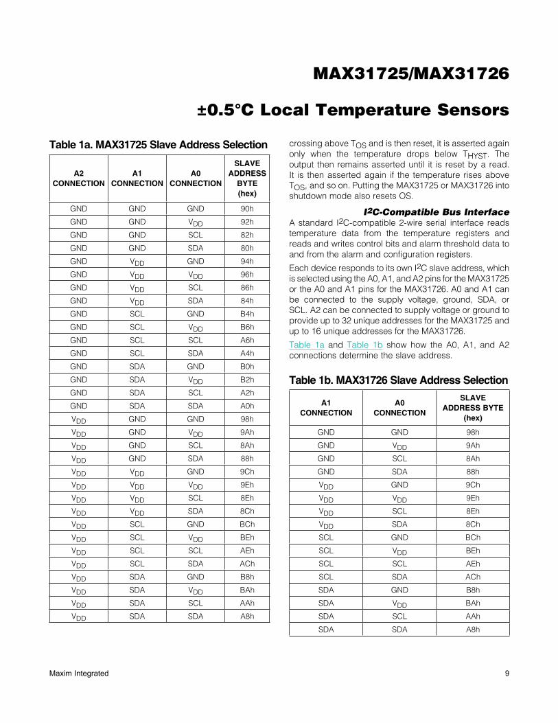
crossing above TOS and is then reset, it is asserted again only when the temperature drops below THYST. The output then remains asserted until it is reset by a read. It is then asserted again if the temperature rises above TOS, and so on. Putting the MAX31725 or MAX31726 into shutdown mode also resets OS.
I2C-Compatible Bus InterfaceA standard I2C-compatible 2-wire serial interface reads temperature data from the temperature registers and reads and writes control bits and alarm threshold data to and from the alarm and configuration registers.
Each device responds to its own I2C slave address, which is selected using the A0, A1, and A2 pins for the MAX31725 or the A0 and A1 pins for the MAX31726. A0 and A1 can be connected to the supply voltage, ground, SDA, or SCL. A2 can be connected to supply voltage or ground to provide up to 32 unique addresses for the MAX31725 and up to 16 unique addresses for the MAX31726.
Table 1a and Table 1b show how the A0, A1, and A2 connections determine the slave address.
Table 1a. MAX31725 Slave Address Selection
Table 1b. MAX31726 Slave Address Selection
A2 CONNECTION
A1 CONNECTION
A0 CONNECTION
SLAVE ADDRESS
BYTE (hex)
GND GND GND 90h
GND GND VDD 92h
GND GND SCL 82h
GND GND SDA 80h
GND VDD GND 94h
GND VDD VDD 96h
GND VDD SCL 86h
GND VDD SDA 84h
GND SCL GND B4h
GND SCL VDD B6h
GND SCL SCL A6h
GND SCL SDA A4h
GND SDA GND B0h
GND SDA VDD B2h
GND SDA SCL A2h
GND SDA SDA A0h
VDD GND GND 98h
VDD GND VDD 9Ah
VDD GND SCL 8Ah
VDD GND SDA 88h
VDD VDD GND 9Ch
VDD VDD VDD 9Eh
VDD VDD SCL 8Eh
VDD VDD SDA 8Ch
VDD SCL GND BCh
VDD SCL VDD BEh
VDD SCL SCL AEh
VDD SCL SDA ACh
VDD SDA GND B8h
VDD SDA VDD BAh
VDD SDA SCL AAh
VDD SDA SDA A8h
A1 CONNECTION
A0 CONNECTION
SLAVE ADDRESS BYTE
(hex)
GND GND 98h
GND VDD 9Ah
GND SCL 8Ah
GND SDA 88h
VDD GND 9Ch
VDD VDD 9Eh
VDD SCL 8Eh
VDD SDA 8Ch
SCL GND BCh
SCL VDD BEh
SCL SCL AEh
SCL SDA ACh
SDA GND B8h
SDA VDD BAh
SDA SCL AAh
SDA SDA A8h

MAX31725/MAX31726
±0.5°C Local Temperature Sensors
10Maxim Integrated
Internal RegistersThe device contains four registers, each of which consists of 2 bytes. The configuration register contains only 1 byte of actual data and, when read as a 2-byte register, repeats the same data for the second byte. During a 2-byte write to the configuration register the second byte written takes precedence. The device’s pointer register selects between the four data registers shown in Table 2. During reads and writes the pointer register auto increments after every 2 data bytes, but does not wrap from address 03h-00h. The pointer register must
be written for each I2C transaction. All registers are read and write, except for the read-only temperature register.
Write to the configuration register by writing the slave address byte, the pointer register byte to value 01h, and a data byte. The TOS and THYST registers require the slave address byte, pointer register byte, and 2 data bytes. If only 1 data byte is written, it is saved in bits D[15:8] of the respective register. If more than 2 data bytes are written, the pointer register auto increments and if pointing to a valid address, additional data writes to the next address. See Figure 3.
Table 2. Register Functions and POR State
Figure 3. I2C-Compatible Timing Diagram (Write)
REGISTER NAME
ADDRESS(Hex)
POR STATE POR STATE(°C)
READ/WRITEHex BINARY
Temperature 00 0000h 0000 0000 0000 0000 0 Read-only
ConfigurationMAX31725
01 00h 0000 0000 — R/W
ConfigurationMAX31726
01 40h 0100 0000 — R/W
THYST 02 4B00h 0100 1011 0000 0000 75 R/W
TOS 03 5000h 0101 0000 0000 0000 80 R/W
ADDRESSBYTE
ADDRESSBYTE
(a) CONFIGURATION REGISTER WRITE.
(b) TOS AND THYST WRITE.
POINTERBYTE
POINTERBYTE
MOST SIGNIFICANTDATA BYTE
LEAST SIGNIFICANTDATA BYTE
CONFIGURATIONBYTE
ACK BYMAX31725/MAX31726
ACK BYMAX31725/MAX31726
ACK BYMAX31725/MAX31726
ACK BYMAX31725/MAX31726
ACK BYMAX31725/MAX31726
STARTBY
MASTER
STARTBY
MASTER
ACK BYMAX31725/MAX31726
ACK BYMAX31725/MAX31726
STOPCOND BYMASTER
STOPCOND BYMASTER
D1 D01 0 D3*D4*D5* D2* D1* R/W 000 000
D0D1D2D3D4D5D6D7D0D1D0D1 D2D3D4D5D6D7
D0D1D2D3D4D5D6D7
1 0 0 0 0 0 0 0D3*D4*D5* D2* D1* R/W
1 1 1 19 9 9 9
1 1 19 9 9
*SEE TABLE 1A.

MAX31725/MAX31726
±0.5°C Local Temperature Sensors
11Maxim Integrated
Table 3. Temperature, THYST, and TOS Register Definition
Figure 4. I2C-Compatible Timing Diagram (Read)
Perform a read operation by issuing the slave address byte (write), pointer byte, repeat START, another slave address byte (read), and then reading the data byte. After 2 data bytes the pointer register auto increments and, if pointing to a valid address, additional data can be read. See Figure 4.
Temperature RegistersTemperature data is stored in the temperature, TOS set point, and THYST set point registers. The temperature data format is 16 bits, two’s complement, and the register is read out in 2 bytes: an upper byte and a lower byte.
Bits D[15:0] contains the temperature data, with the LSB representing 0.00390625NC and the MSB representing the sign bit; see Table 3. The MSB is transmitted first.
In addition to the normal two’s complement temperature data format, the MAX31725 and MAX31726 offer an optional extended data format that allows temperatures equal to or greater than +128NC to be read. In the extended format, selected by bit 5 of the configuration register, the measured temperature is the value in the temperature register plus 64NC, as shown in Table 4.
UPPER BYTE LOWER BYTE
D15 D14 D13 D12 D11 D10 D9 D8 D7 D6 D5 D4 D3 D2 D1 D0
S
MSB
64NC32NC 16NC 8NC 4NC 2NC 1NC 0.5NC 0.25NC 0.125NC 0.0625NC 0.03125NC 0.015625NC 0.0078125NC 0.00390625NC
26 25 24 23 22 21 20 2-1 2-2 2-3 2-4 2-5 2-6 2-7 2-8
ADDRESS BYTE
ADDRESSBYTE
(b) TYPICAL POINTER SET FOLLOWED BY IMMEDIATE READ FOR 2-BYTE REGISTER SUCH AS TEMPERATURE, TOS, AND THYST.
POINTER BYTE
MOST SIGNIFICANTDATA BYTE
LEAST SIGNIFICANTDATA BYTE
ACK BYMAX31725/MAX31726
ACK BYMAX31725/MAX31726
ACK BYMASTER
ACK BYMAX31725/MAX31726
STARTBY
MASTER
1
1 0 0 0 0 0 0 0D3*D4*D5* D2* D1* D1 D0
19 9
REPEATSTART
BYMASTER
STOPCOND BYMASTER
NO ACK BYMASTER
1 19 19 9
R/W
1 0 D3*D4* D7 D6 D5 D4 D3 D2 D1 D0 D7 D6 D5 D4 D3 D2 D1 D0D5* D2* D1* R/W
ADDRESSBYTE
(a) TYPICAL POINTER SET FOLLOWED BY IMMEDIATE READ FROM CONFIGURATION REGISTER.
POINTERBYTE
ADDRESSBYTE
DATABYTE
ACK BYMAX31725/MAX31726
ACK BYMAX31725/MAX31726
STARTBY
MASTERREPEATSTART
BYMASTER
NOACK BYMASTER
STOPCOND BYMASTER
ACK BYMAX31725/MAX31726
1 0 D3*D4*D5* D2* D1* R/W 00 D1 D0 D0D1D2D3D4D5D6D700000 1 D3*D4*D5* D2* D1* R/W
1 1 1 19 9 9 9
*SEE TABLE 1A.

MAX31725/MAX31726
±0.5°C Local Temperature Sensors
12Maxim Integrated
Configuration RegisterThe configuration register contains 8 bits of data and initiates single conversions (ONE-SHOT), enables bus timeout, controls shutdown, sets the fault queue, sets the data format, selects OS polarity, and determines whether the OS output functions in comparator or interrupt mode. See Table 5.
ShutdownSet bit D0 to 1 to place the device in shutdown mode and reduce supply current to 3.5FA or less. If bit D0 is set to 1 when a temperature conversion is taking place, the device completes the conversion and then shuts down. In interrupt mode, entering shutdown resets the OS output. While in shutdown, the I2C interface remains active and all registers remain accessible to the master.
Setting D0 to 0 takes the device out of shutdown and starts a new conversion. The results of this conversion are available to read after the max conversion time.
COMPARATOR/INTERRUPT ModeSet bit D1, the COMPARATOR/INTERRUPT bit to 0 to operate OS in comparator mode. In comparator mode, OS is asserted when the temperature rises above the TOS value. OS is deasserted when the temperature drops below the THYST value. See Figure 2.
Set bit D1 to 1 to operate OS in interrupt mode. In interrupt mode, exceeding TOS also asserts OS. OS remains asserted until a read operation is performed on any of the registers. Once OS has asserted due to crossing above TOS and is then reset, it is asserted again only when the temperature drops below THYST. The output then remains asserted until it is reset by a read. It is then asserted again if the temperature rises above TOS, and so on. Putting the MAX31725 into shutdown mode also resets OS. Note that if the mode is changed while OS is active, an OS reset may be required before it begins to behave normally.
OS PolaritySet bit D2, the OS POLARITY bit, to 0 to force the OS output polarity to active low. Set bit D2 to 1 to set the OS output polarity to active high. OS is an open-drain output under all conditions and requires a pullup resistor to output a high voltage. See Figure 2.
Fault QueueBits D4 and D3, the fault queue bits, determine the number of faults necessary to trigger an OS condition. See Table 6. The number of faults set in the queue must occur consecutively to trip the OS output. The fault queue prevents OS false tripping in noisy environments.
Table 4. Temperature Data Output Format
Table 5. Configuration Register Definition
TEMPERATURE (°C)NORMAL FORMAT EXTENDED FORMAT
BINARY Hex BINARY Hex
+150 0111 1111 1111 1111 7FFFh 0101 0110 0000 0000 5600h
+128 0111 1111 1111 1111 7FFFh 0100 0000 0000 0000 4000h
+127 0111 1111 0000 0000 7F00h 0011 1111 0000 0000 3F00h
+125 0111 1101 0000 0000 7D00h 0011 1101 0000 0000 3D00h
+64 0100 0000 0000 0000 4000h 0000 0000 0000 0000 0000h
+25 0001 1001 0000 0000 1900h 1101 1001 0000 0000 D900h
+0.5 0000 0000 1000 0000 0080h 1100 0000 1000 0000 C080h
0 0000 0000 0000 0000 0000h 1100 0000 0000 0000 C000h
-0.5 1111 1111 1000 0000 FF80h 1011 1111 1000 0000 BF80h
-25 1110 0111 0000 0000 E700h 1010 0111 0000 0000 A700h
-55 1100 1001 0000 0000 C900h 1000 1001 0000 0000 8900h
D7 D6 D5 D4 D3 D2 D1 D0
ONE-SHOT TIMEOUTDATA
FORMATFAULT
QUEUE [1]FAULT
QUEUE [0]OS
POLARITYCOMPARATOR/
INTERRUPTSHUTDOWN

MAX31725/MAX31726
±0.5°C Local Temperature Sensors
13Maxim Integrated
Data FormatBit D5 selects the temperature data format for the temperature, TOS, and THYST registers. When D5 is 0 (normal format), the data format is two’s complement with a range of -128NC to +127.99609375NC.
Set D5 to 1 for extended temperature format. In extended format, the measured temperature equals the two’s complement value plus 64NC, thereby extending the upper temperature data range to 191.99609375NC and allowing temperatures as high as 150NC to be measured. See Table 4. Once set, the data format does not update until the completion of the following temperature conversion. After setting D5 to 1, new extended temperature data is guaranteed ready after a time equal to twice the max conversion time.
TIMEOUT EnableSet D6 to 1 to disable bus timeout.
Set D6 to 0 to reset the I2C-compatible interface when SDA is low for more than 50ms (nominal).
One-ShotThe ONE-SHOT function helps to reduce average supply current when continuous conversions are not necessary. Setting D7 to 1 while the device is in shutdown mode immediately begins a new temperature conversion. After the conversion has completed, the device returns to shutdown mode. D7 returns to 0 when the conversion completes. Writing 1 to D7 has no effect when the device is not in shutdown.
Power-On Reset ValueThe configuration register always powers up to a known state, as indicated in Table 2. These default POR values correspond to the following modes of operation:
• Comparator mode
• OS active low
• 1 fault, fault queue
• Normal data format
• Timeout enabled for MAX31725; timeout disabled for MAX31726
RESET Input (MAX31726 Only)The RESET input on the MAX31726 provides a way to reset the I2C bus and all the internal registers to their initial POR values. To reset, apply a low pulse width a duration of at least the minimum reset pulse width
(tRESET) to the RESET input.
Applications Information
The MAX31725 and MAX31726 measure the temperature of their own die. The thermal path between the die and the outside world determines the accuracy of temperature measurements. External temperature is conducted to the die primarily through the leads and the exposed pad. Because of this, the device most easily measures the PCB temperature. For ambient temperature measurements, mount the device on a PCB (or a section of the PCB) that is at ambient temperature. Temperature errors due to self-heating of the device die are minimal due to the low supply current.
Digital Noise IssuesBoth devices feature an integrated lowpass filter on the SCL and SDA digital lines to mitigate the effects of bus noise. Although this filtering makes communication robust in noisy environments, good layout practices are always recommended. Minimize noise coupling by keeping digital traces away from switching power supplies. Ensure that digital lines containing high-speed data cross at right angles to the SDA and SCL lines. Excessive noise coupling into the SDA and SCL lines on the device—specifically noise with amplitude greater than 400mVP-P (typical hysteresis), overshoot greater than 300mV above +VDD, and undershoot more than 300mV below GND—can prevent successful serial communication. Serial bus not-acknowledge is the most common symptom, causing unnecessary traffic on the bus. Care must be taken to ensure proper termination within a system with long PCB traces or multiple slaves on the bus. Resistance can be added in series with the SDA and SCL lines to further help filter noise and ringing. If it proves to be necessary, a 5kI resistor should be placed in series with the SCL line, placed as close as possible to the SCL pin. This 5kI resistor, with the 5pF to 10pF stray capacitance of the device provide a 6MHz to 12MHz lowpass filter, which is sufficient filtering in most cases.
Table 6. Configuration Register Fault Queue Bits
FAULT QUEUE [1]BIT D4
FAULT QUEUE [0]BIT D3
NUMBER OF FAULTS
0 0 1 (POR state)
0 1 2
1 0 4
1 1 6

MAX31725/MAX31726
±0.5°C Local Temperature Sensors
14Maxim Integrated
Package Information
For the latest package outline information and land patterns (footprints), go to www.maximintegrated.com/packages. Note that a “+”, “#”, or “-” in the package code indicates RoHS status only. Package drawings may show a different suffix character, but the drawing pertains to the package regardless of RoHS status.
Ordering Information
+Denotes a lead(Pb)-free/RoHS-compliant package.*EP = Exposed pad.
PART TEMP RANGE RESET TIMEOUT ENABLED AT POR PIN-PACKAGE
MAX31725MTA+ -55NC to +150NC No Yes 8 TDFN-EP*
MAX31726MTA+ -55NC to +150NC Yes No 8 TDFN-EP*
PACKAGE TYPE PACKAGE CODE OUTLINE NO. LAND PATTERN NO.
8 TDFN-EP T833+2 21-0137 90-0059

MAX31725/MAX31726
±0.5°C Local Temperature Sensors
Maxim Integrated cannot assume responsibility for use of any circuitry other than circuitry entirely embodied in a Maxim Integrated product. No circuit patent licenses are implied. Maxim Integrated reserves the right to change the circuitry and specifications without notice at any time. The parametric values (min and max limits) shown in the Electrical Characteristics table are guaranteed. Other parametric values quoted in this data sheet are provided for guidance.
Maxim Integrated 160 Rio Robles, San Jose, CA 95134 USA 1-408-601-1000 15© 2014 Maxim Integrated Products, Inc. Maxim Integrated and the Maxim Integrated logo are trademarks of Maxim Integrated Products, Inc.
Revision History
REVISIONNUMBER
REVISIONDATE
DESCRIPTIONPAGES
CHANGED
0 9/12 Initial release —
1 3/13 Added the MAX31726 All
2 12/14 Updated Benefits and Features section 1