machxo cpld training module
DESCRIPTION
MachXO CPLD Training Module. What you will learn in this module: MachXO technology MachXO Features & Benefits MachXO Competition Applications & Target Markets How to sell MachXO solutions. SC. 500MHz Fabric 2Gbps I/O with INDEL & AIL circuitry. I/O: 139 - 944. EBR: 1.0 - 7.8Mb. - PowerPoint PPT PresentationTRANSCRIPT
Basic Module - Mach XO
1
MachXO CPLD Training Module
What you will learn in this module:
1. MachXO technology
2. MachXO Features & Benefits
3. MachXO Competition
4. Applications & Target Markets
5. How to sell MachXO solutions

Basic Module - Mach XO
2
XP2I/O: 86 - 540 EBR: 166 - 885Kb
“Instant On” Devices
Lattice Product Matrix
Density (LUTs)10k 20k 30k 40k 50k 60k 70k 80k 90k 100k 110k
90m
ispCLKOutputs: 4 - 20
POWRInputs: 6 - 12Outputs: 6 - 28
Mixed Signal Devices
ECP2I/O: 90 - 588 EBR: 55 - 1100Kb
300MHz Fabric840Mbps I/O
ECP2MI/O: 144 - 601 EBR: 1.2 - 5.3Mb
300MHz Fabric840Mbps I/O
SCI/O: 139 - 944 EBR: 1.0 - 7.8Mb
500MHz Fabric2Gbps I/O with INDEL & AIL circuitry
90m
130
m
Macrocell: 32-512, I/O: 32 - 212
4K
/ZE
SRAM FPGAs
LUT: 256-2280, I/O: 78 - 271, EBR: 0 - 27KbXO

Basic Module - Mach XO
3
MachXO Technology
MachXO is a Crossover PLD: Combines features of CPLDs & FPGAs
CPLD Features “Instant-on” Non-volatile High pin/logic ratio Pin-to-pin speed 3.5ns
FPGA Features SRAM-based Optimized LUT fabric Integrated PLLs Embedded Memory Blocks Internal Oscillator
So what’s a LUT ?
130nm FLASH process from Fujitsu 256 to 2280 LUTs 78 to 271 I/Os

Basic Module - Mach XO
4
MachXO Technology – LUT
MachXO uses a 4-input Look Up Table (LUT)
Can create any 4-input combinatorial function
256 to 2280 LUTs in the XO family
LUT is automatically ‘mapped’ based on behavioral description or schematic instance
4-Input LUT
ABCD
Y
ABCD
Y
A
Y
B
C
D
ABCD
Y
Look Up Table (LUT) – the Swiss army knife of combinational logic
Basic Module - Mach XO
5
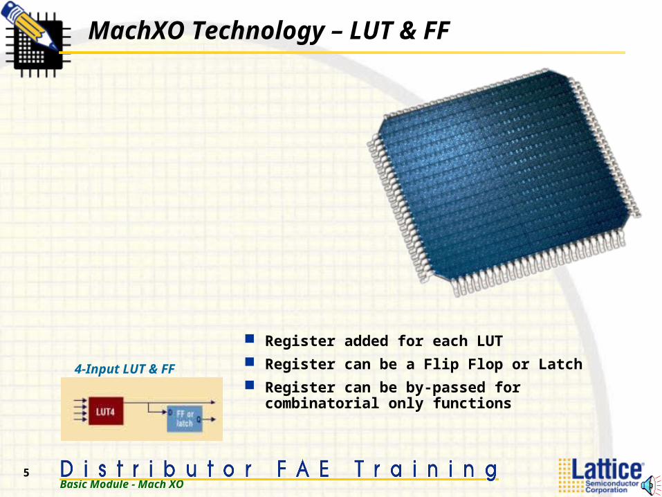
MachXO Technology – LUT & FF
Register added for each LUT
Register can be a Flip Flop or Latch
Register can be by-passed for combinatorial only functions
4-Input LUT & FF

Basic Module - Mach XO
6
MachXO Technology – Slice
Slice consists of 2 LUT/Flip Flop pairs Slice has common CLK, CE, SET & RST for both FFs Multiple LUTs combined for larger functions Carry chain for fast arithmetic functions
Slice
Carry In
Basic Module - Mach XO
7
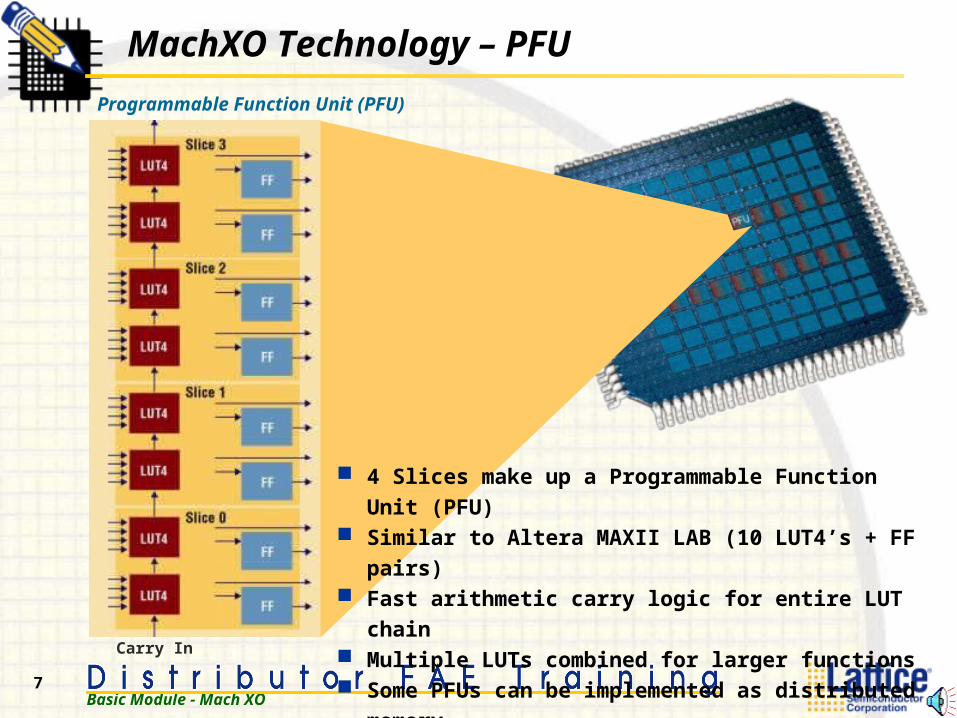
MachXO Technology – PFU
Programmable Function Unit (PFU)
Carry In
4 Slices make up a Programmable Function Unit (PFU) Similar to Altera MAXII LAB (10 LUT4’s + FF pairs) Fast arithmetic carry logic for entire LUT chain Multiple LUTs combined for larger functions Some PFUs can be implemented as distributed memory

Basic Module - Mach XO
8
1 PFU can be configured as the following distributed memory:
MachXO Technology – Distributed Memory
Memory sizes can be expanded with extra PFUs
ROMs can be implemented in any PFU
RAMs can be implemented in some of the PFUs
Typical performance 250 to 400 MHz
AD[3:0]
DI[7:0]
WCK
WRE
DO[7:0]
16x8 Single Port RAM
WAD[3:0]
DI[3:0]
WCK
WRE
RAD[3:0]
RDO[3:0]
WDO[3:0]
16x4 Pseudo-Dual Port RAM
AD[3:0] DO[7:0]
16x8 ROM
WCK128 bits/PFU
Basic Module - Mach XO
9
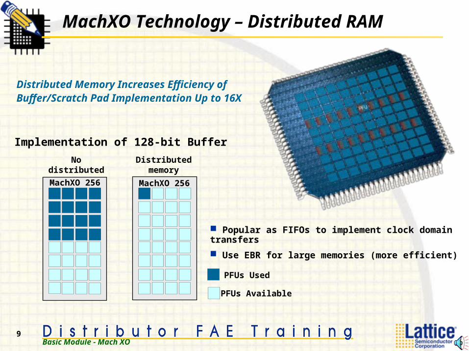
Distributed Memory Increases Efficiency of Buffer/Scratch Pad Implementation Up to 16X
No distributed memory
Distributedmemory
Implementation of 128-bit Buffer
MachXO 256 MachXO 256
PFUs Used
PFUs Available
MachXO Technology – Distributed RAM
Popular as FIFOs to implement clock domain transfers
Use EBR for large memories (more efficient)

Basic Module - Mach XO
10
sysMEM Embedded Block RAM (EBR) Provides 9k bit blocks (1 in 1220, 3 in 2280) 275MHz Operation Efficient Implementation of Memory Buffers Use EBRs for large blocks of memory
MachXO Technology – sysMEM EBR
8192x1 1024x4
4096x2 512x18
2048x4 256x36**Not available for dual port
sysMEMConfiguration
OptionsAD[12:0]
DI[35:0]CLKRSTWE
CS[2:0]
DO[35:0]
RAM(Single Port)
EBR
AD[12:0]
DIA[17:0]CLKARSTAWEA
CSA[2:0]
ADB[12:0]DIB[17:0]CLKBRSTBWEBCSB[2:0]DOB[17:0]
RAM(Dual Port)
EBR
DOA[17:0]
FIFO (includes control logic)
EBR
DO[35:0]CLKRRSTBRERCEFFAFEFAE
DI[35:0]
CLKBRSTA
WECEW
WAD[12:0]
WD[35:0]WCLK
WCEWE
RST
RAD[12:0]RD[35:0]RCERCLK
RAM(Pseudo Dual Port)
EBR
AD[12:0]
CLK
CE
DO[35:0]
ROM
EBR
Basic Module - Mach XO
11
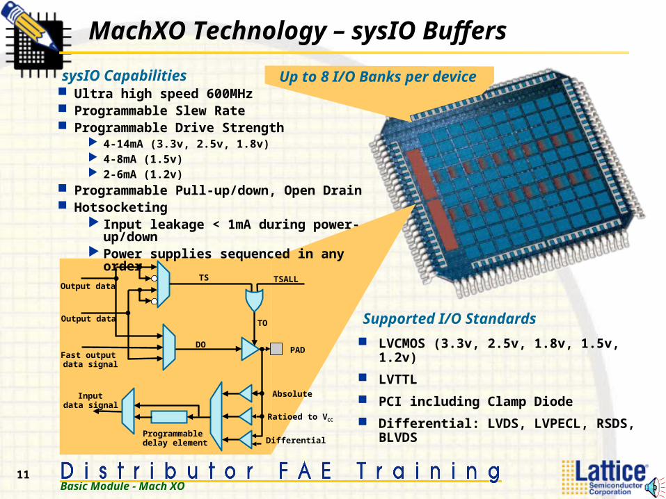
MachXO Technology – sysIO Buffers
LVCMOS (3.3v, 2.5v, 1.8v, 1.5v, 1.2v)
LVTTL
PCI including Clamp Diode
Differential: LVDS, LVPECL, RSDS, BLVDS
Supported I/O Standards
sysIO Capabilities
PAD
TO
Programmable delay element
Inputdata signal
Output data
Fast output data signal
TSALL
DO
TS
Output data
Absolute
Ratioed to VCC
Differential
Ultra high speed 600MHz Programmable Slew Rate Programmable Drive Strength
4-14mA (3.3v, 2.5v, 1.8v) 4-8mA (1.5v) 2-6mA (1.2v)
Programmable Pull-up/down, Open Drain Hotsocketing
Input leakage < 1mA during power-up/down Power supplies sequenced in any order
Up to 8 I/O Banks per device
Basic Module - Mach XO
12
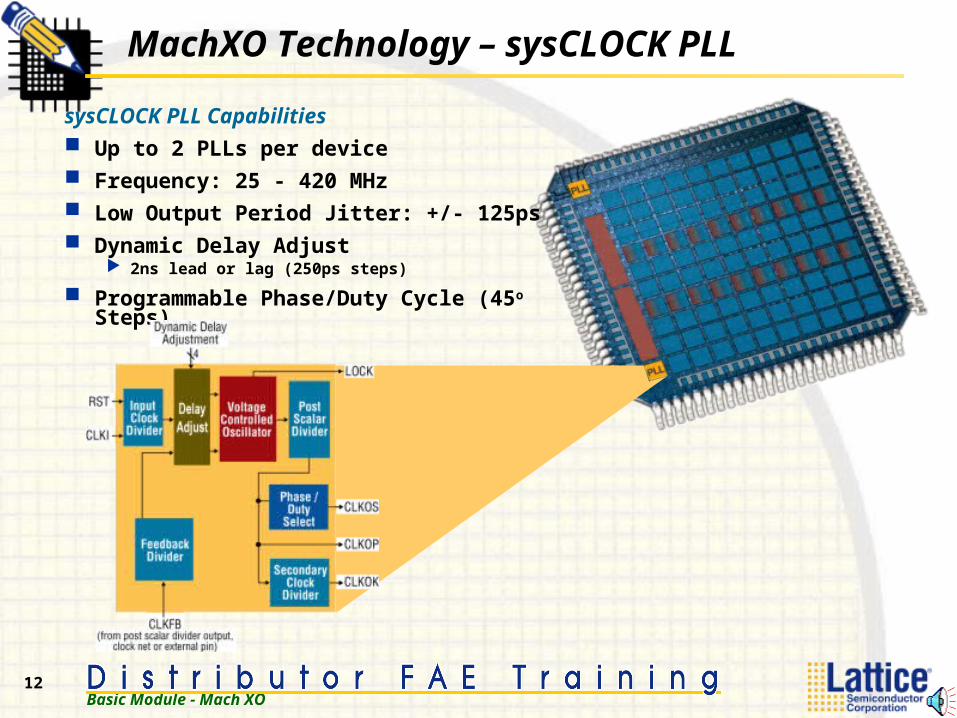
MachXO Technology – sysCLOCK PLL
sysCLOCK PLL Capabilities Up to 2 PLLs per device Frequency: 25 - 420 MHz Low Output Period Jitter: +/- 125ps Dynamic Delay Adjust
2ns lead or lag (250ps steps)
Programmable Phase/Duty Cycle (45o Steps)
Basic Module - Mach XO
13
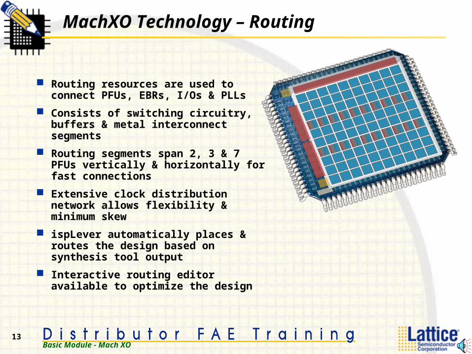
MachXO Technology – Routing
Routing resources are used to connect PFUs, EBRs, I/Os & PLLs
Consists of switching circuitry, buffers & metal interconnect segments
Routing segments span 2, 3 & 7 PFUs vertically & horizontally for fast connections
Extensive clock distribution network allows flexibility & minimum skew
ispLever automatically places & routes the design based on synthesis tool output
Interactive routing editor available to optimize the design

Basic Module - Mach XO
14
On-Chip Oscillator
On-Chip Oscillator Provides Low Cost Clock Ideal for non-timing-critical state machines
Nominal 20Mhz Frequency Tolerance 17 to 24MHz
Drives Internal Routing Can be routed off chip
Powered Off When Not In Use
Easily Implemented With ispLEVER Design Tools
OSCC
OSCLK
Oscillator Primitive
COMPONENT OSCCPORT (OSC:OUT std_logic);
END COMPONENT;
beginOSCInst0: OSCCPORT MAP (OSC => osc_int);
VHDL instance
Basic Module - Mach XO
15
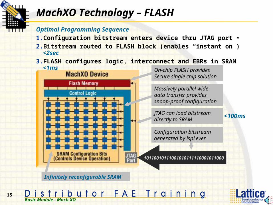
MachXO Technology – FLASH
10110010111001010111110001011000
Optimal Programming Sequence 1. Configuration bitstream enters device thru JTAG port2. Bitstream routed to FLASH block (enables “instant on”) <2sec3. FLASH configures logic, interconnect and EBRs in SRAM <1ms
On-chip FLASH providesSecure single chip solution
Massively parallel wide data transfer provides snoop-proof configuration
Configuration bitstream generated by ispLever
Infinitely reconfigurable SRAM
JTAG can load bitstream directly to SRAM
<100ms

Basic Module - Mach XO
16
MachXO Technology – FLASH
Each sysMEM EBR is Shadowed by Flash Memory Allows each bit to be uniquely initialized
Reprogramming FLASH Allows ROM contents to be changed – user PROM
10111001000111000101100011001011
EBR
ROM at t1
10111001000111000101100011001011
New data Loaded In ROM
11111111000000000000000011111111
EBR
ROM at t3
11111111000000000000000011111111
New dataLoaded in ROM
10111001000111000101100011001011
EBR
ROM at t0
Initial data viaJTAG programming
11111111000000000000000011111111
EBR
ROM at t2
10111001000111000101100011001011
New data via JTAG Programming in background

Basic Module - Mach XO
17
MachXO Technology - Reconfiguration
Reconfiguration Sequence
1. Power-up with configuration #1
2. Background FLASH programming bitstream #2 while logic functions
3. I/O States are locked in user-defined values
4. FLASH transfers bitstream #2 to SRAM
5. Inputs operational, logic initialized, output control reverts to user logic
Transparent Field Reconfiguration (TransFR) Enables in-system field updates while the system operates!

Basic Module - Mach XO
18
MachXO Technology – Supply Voltages
“C” Version Provides Access to Latest Technology Without Adding New Power Supplies to Board
Improved performance and power consumption
Supports single supply operation from 3.3v
Operates internally at 1.2v
“E” Version Minimizes Power Consumption 64% lower power than operation at 3.3v
Operates internally at 1.2v
Supply voltages for MachXO devices can be powered up in any sequence

Basic Module - Mach XO
19
Device Mode
Characteristic Normal Off Sleep
SLEEPN Pin High X Low
Static Icc Typically <10mA 0 Typically <100uA
Power Supplies Normal Range 0 Normal Range
Logic Operation User Defined Non Operational Non Operational
I/O Operation User Defined Tri-State Tri-State
MachXOSLEEPN
Pin
DeviceState
Normal Sleep Mode Normal
<100nS <1mS
Sleep Mode is only available on 1.8/2.5/3.3V “C” version devices
MachXO Technology – Sleep Mode
MachXO consumes 100X less static power in Sleep Mode

Basic Module - Mach XO
20
MachXO Technology – Performance
Description Parameter Performance
Device pin to pin delay tPD 3.5 ns
Device clock pin to out pin delay tCO 4.0 ns
PFU average frequency for various simple functions fMAX 270 MHz
sysMEM EBR average frequency for various RAM sizes fMAX 275 MHz
Clock frequency of sysIO and PFU registers fMAX_IO 600 MHz
sysCLOCK PLL range fIN, fOUT 25 – 420MHz
Performance supports designs > 250MHz
tCO = 4.0ns
D Q
VCLOCK
tPD = 3.5ns
LUT4

Basic Module - Mach XO
21
MachXO Family Members
RoHS
Note: only the XO1200 & XO2280 contain EBRs and PLLs.
ftBGA TQFP csBGA
* Distributed RAM bits are part of the total LUT allocation.
*

Basic Module - Mach XO
22
MachXO – Part Numbers

Basic Module - Mach XO
23
Feature Benefits
Self-Configuration in < 1ms Instant-On ideal for system “heartbeat” control logic
Supports rapid power cycling
Integrates multiple components on a single chip
Simplify design
Reduce PCB footprint
Lower BOM cost (e.g. boot PROM)
Security bits, no exposed power-up bitstream
Very high security
Necessity for military apps
SRAM + FLASH + TransFR Enables in field updates while system is operational
5 nines support (99.999%)
Sleep Mode 100X lower static power (typical < 100uA, usually 10mA)
Enables portable apps
On-chip Regulation Supports legacy apps with latest technology to reduce costs & improve performance
MachXO Features & Benefits
Basic Module - Mach XO
24
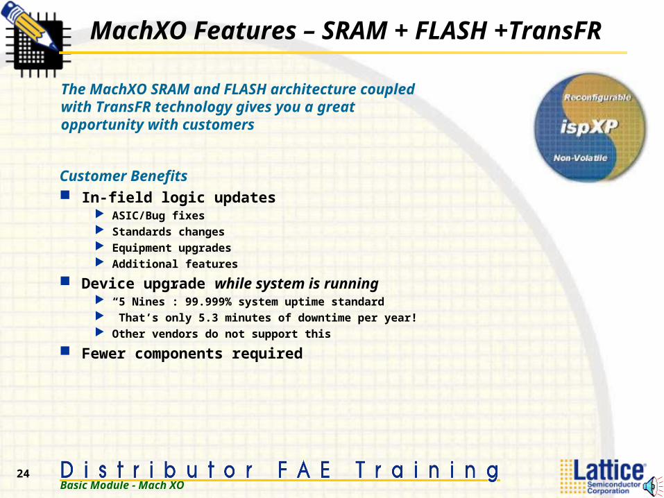
MachXO Features – SRAM + FLASH +TransFR
Customer Benefits In-field logic updates
ASIC/Bug fixes Standards changes Equipment upgrades Additional features
Device upgrade while system is running “5 Nines”: 99.999% system uptime standard That’s only 5.3 minutes of downtime per year! Other vendors do not support this
Fewer components required
The MachXO SRAM and FLASH architecture coupled with TransFR technology gives you a great opportunity with customers

Basic Module - Mach XO
25
MachXO Competition – Altera MAX II
Attribute MAX II MachXO
Technology 180nm SRAM+Flash 130nm SRAM+Flash
Density 240 – 2210 LUTs 256 – 2280 LUTs
I/Os 80 - 272 78 - 271
Logic Implementation 4-input LUT + FF 4-input LUT + FF
Distributed Memory None Yes (2k – 7.7kbits)
Block Memory None Yes (0 – 28kbits)
PLL None 0 – 2
Internal Oscillator Yes Yes
I/O LVCMOS/PCI LVCMOS/PCILVDS
User Flash 8K bits EBR shadowed by Flash
Power 2-10mA Static 2-10mA Static<100uA Sleep mode
In Field Updates Part tri-states during refresh
TransFR Technology
Voltage 1.8/2.5/3.3v 1.2/1.8/2.5/3.3v

Basic Module - Mach XO
26
MachXO Competition - Actel ProASIC 3Attribute Actel ProASIC 3 MachXO
Technology 130nm Flash 130nm SRAM+Flash
Density 307 – 30k LUTs* 256 – 2280 LUTs
I/Os 81 – 616 78 – 271
Logic Implementation Primitive tiles 4-input LUT + FF
Distributed Memory None Yes (2k – 7.7kbits)
Block Memory Yes (0 – 147kbits) Yes (0 – 28kbits)
PLL 0 – 1 0 – 2
Internal Oscillator No Yes
I/O LVCMOS/PCI/PCI-XHotsocketing**LVDS (Emulated)***
LVCMOS/PCIHotsocketingLVDS
User Flash 1K Bits Programmed Through JTAG
EBR Shadowed by Flash
Security Flash LockAES Encryption (except A3P030)
Security Scheme Prevents Readback
Power 10-50mA Static 2-10mA Static<100uA Sleep Mode
In Field Updates Long Programming Time Limits Field Updates While Equipment Operates
TransFR Technology
Voltage 1.5v (3.3v Programming) 1.2/1.8/2.5/3.3v
* Assumes 2.5 Tiles = 1 LUT ** Lowest density device only *** Above 2.5K LUTs

Basic Module - Mach XO
27
MachXO Target Markets Industrial: high temp range, high pin/logic ratio
Hand-held Computing: ultra low power sleep mode
Military: security, instant-on
Automotive: high temp range great for cabin apps
Consumer: multiple device integration, small footprint, low cost
Here’s where we really shine!
MachXO Apps & Target MarketsMachXO General Applications Bus Interface Bus Bridging Data Conversion Chip Select Power & Reset Control ASIC & FPGA Configuration Memory Control Signal Distribution System Power Management Small ASIC/ASSP Replacement ASIC Bug Fixes
Basic Module - Mach XO
28
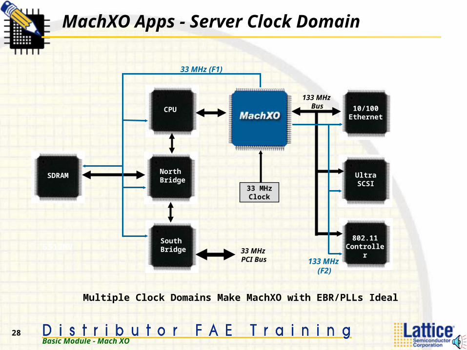
MachXO Apps - Server Clock Domain
10/100Ethernet
UltraSCSI
802.11Controller
North Bridge
33 MHz PCI Bus
133 MHz BusCPU
SDRAM
South Bridge5512MV
33 MHz (F1)
133 MHz (F2)
5512MV
33 MHzClock
MachXO
Multiple Clock Domains Make MachXO with EBR/PLLs Ideal

Basic Module - Mach XO
29
MachXO Apps - Server Clock Domain (PLL)
CLK IN (33 MHZ)
CLK 1 OutTo CPU and Bridges
Peripheral Bus
F1 (33 MHZ)
F2 (133 MHZ)
16-BitReg
16-BitReg
CPU Bus
PLL0
N = 0
M = 2 V = 10VCOPGMDLY
K
PLL_Lock
Sec_OutPLL_FBK
N = 0
M = 8 V = 5VCOPGMDLY
K
PLL_Lock
Sec_OutPLL_FBK
PLL1
VCO Freq = 330 MHz
CLK 2 OutTo Peripheral Devices
MachXO Solution Utilize 2 PLLs FIFO’s for Data Buffering EBRs Minimum Skew
VCO Freq = 665 MHz
Basic Module - Mach XO
30
XO2280 Leave Alone I/O 1400 LUTs 130 LVTTL I/O Instant-On 3 EBRs & 1 PLL
MachXO Apps - Base Station Solution
MPU(RISC or
CISC)
FlashMemory
SRAM
SystemGlue Logic
PowerSupply
ControlLogic
MCPA
LNA
System Controller Unit
Filtering
RF RxRF Tx
BroadbandInterface
Logic
ADC
DAC ADC
Filtering
Symbol Encode &
Modulation
Symbol Decode &
Demodulation
DC-DCpower supply
PHYInterfaceCircuitry
CircuitSwitch
Control &Signaling
Multi-Carrier Power
Amplifier
BSCInterface
Rx/Tx
Rx
EI/TI
Baseband Unit
Network Interface Unit
Basic Module - Mach XO
31
MachXO Apps - Node B Remote Radio Head
Power Quicc II
SRAMMPC 60x
FLASH
Ethernet
MAC
Hig
h S
pe
ed
B
loc
k
Utopia, BSII & I2C
Te
rmin
al
Co
ntr
ol
Terminal Bus
Terminal
Clo
ck
D
istr
ibu
tio
n
FP
GA
Lo
ad
er
XO2280 2200 LUTS
160 I/O
2 PLLs
3 EBRs

Basic Module - Mach XO
32
Under-The-Hood• ABS Brakes• Electronic Throttle• Fuel Cell Controller• Hybrid Battery Controller• Powertrain• Regenerative Braking• Transmission
Advanced Safety Systems• Active Steering• Adaptive Cruise Control• Lane Keeping Assist• Navigation-linked cruise Control• Park/Reverse Assist• Side View Camera• Telematics• Adaptive Headlights• Driver Monitoring• Night View Heads-up display• x-by-wire• Virtual Networks
Entertainment• Digital Radio• Radio / HD Radio / DAB• Surround Sound• Telematics• CD/MP3 Player• DVD Player• GPS• Internet Access
Body Electronics• Protocol Gateway• Accelerator and Brake Petal Adjustments• Air Bags• Biometrics• Memory Seats• Mirrors• Trip Computer• Windows
Lattice Designed Into ProductOpportunity for Lattice Devices
MachXO Apps - Automotive
MachXO is TS-16949 Certified!
Basic Module - Mach XO
33
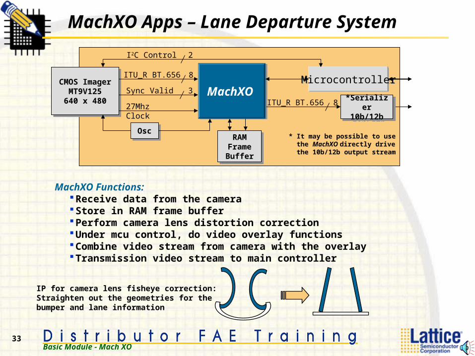
MachXO Apps – Lane Departure System
MachXO Functions:Receive data from the cameraStore in RAM frame bufferPerform camera lens distortion correctionUnder mcu control, do video overlay functionsCombine video stream from camera with the overlayTransmission video stream to main controller
IP for camera lens fisheye correction:Straighten out the geometries for the bumper and lane information
MachXO MachXO CMOS Imager
MT9V125640 x 480
CMOS Imager MT9V125640 x 480
I2C Control
8ITU_R BT.656
27Mhz Clock
Sync Valid
2
3MicrocontrollerMicrocontroller
8ITU_R BT.656
OscOscRAM
Frame Buffer
RAMFrame Buffer
* It may be possible to use the MachXO directly drive the 10b/12b output stream
*Serializer10b/12b
*Serializer10b/12b

Basic Module - Mach XO
34
MachXO - How to Sell
For customers who need a small FPGA XO has SRAM-based LUT architecture, PLLs, distributed memory & EBRs
For customers who need a CPLD XO is non-volatile XO has fast timing (3.5ns pin to pin) XO is sized to the largest industry CPLD
Know our advantages Over MAXII Transparent field reconfigurable (TransFR) Sleep mode provides <100uA static Icc
Integrated PLLs & EBR
If customer insists on a CPLD don’t “unsell” him CPLD has higher ASPs Mach 4000 family has long production life cycle Don’t cannibalize existing Lattice sockets
Sell up Highlight MachXO’s added capabilities/features that can help his design Suggest integrating more board functions & migrate to Lattice XP family
MachXO is aCrossover PLD

Basic Module - Mach XO
35
MachXO – Review Questions
Is MachXO a CPLD or an FPGA?
What is the fastest pin to pin delay with MachXO?
How many LUTs are in a MachXO Slice? PFU?
What 3 capabilities does Flash enable on the MachXO devices?
Name 3 I/O standards supported by MachXO.
When should you use EBR instead of distributed RAM? Why?
What is standby current in sleep mode for MachXO devices?
What MachXO devices contain PLLs? EBRs?
What design system speed does MachXO support?
Name 3 applications well suite to MachXO.
Do you know the answers to the following review questions?

Basic Module - Mach XO
36
MachXO - Summary
Top 3 things to remember about MachXO: MachXO has the fast performance of a CPLD (3.5ns pin to pin)
MachXO has the flexibility & high end functions of an FPGA (PLL, EBR)
MachXO has superior value & features compared to Altera MaxII
Next Steps: Review the MachXO Product Brochure (eLearn “Sparkle Sheets” section)
Print the MachXO Part # Guide, page 22.
Review the customer presentation (eLearn “Customer Presentation” section)
Take the MachXO Quiz