magnetic fields maximilian assig, markus etzkorn, axel ... · review of scientific instruments 84,...
TRANSCRIPT

A 10 mK scanning tunneling microscope operating in ultra high vacuum and highmagnetic fields
Maximilian Assig, Markus Etzkorn, Axel Enders, , Wolfgang Stiepany, Christian R. Ast, , and Klaus Kern
Citation: Review of Scientific Instruments 84, 033903 (2013); doi: 10.1063/1.4793793View online: http://dx.doi.org/10.1063/1.4793793View Table of Contents: http://aip.scitation.org/toc/rsi/84/3Published by the American Institute of Physics

REVIEW OF SCIENTIFIC INSTRUMENTS 84, 033903 (2013)
A 10 mK scanning tunneling microscope operating in ultra high vacuumand high magnetic fields
Maximilian Assig,1 Markus Etzkorn,1 Axel Enders,1,a) Wolfgang Stiepany,1
Christian R. Ast,1,b) and Klaus Kern1,2
1Max-Planck-Institut für Festkörperforschung, 70569 Stuttgart, Germany2Institut de Physique de la Matière Condensée, Ecole Polytechnique Fédérale de Lausanne, 1015 Lausanne,Switzerland
(Received 20 December 2012; accepted 16 February 2013; published online 8 March 2013)
We present design and performance of a scanning tunneling microscope (STM) that operates at tem-peratures down to 10 mK providing ultimate energy resolution on the atomic scale. The STM isattached to a dilution refrigerator with direct access to an ultra high vacuum chamber allowing insitu sample preparation. High magnetic fields of up to 14 T perpendicular and up to 0.5 T parallel tothe sample surface can be applied. Temperature sensors mounted directly at the tip and sample po-sition verified the base temperature within a small error margin. Using a superconducting Al tip anda metallic Cu(111) sample, we determined an effective temperature of 38 ± 1 mK from the thermalbroadening observed in the tunneling spectra. This results in an upper limit for the energy resolutionof �E = 3.5kBT = 11.4 ± 0.3 μeV. The stability between tip and sample is 4 pm at a temperatureof 15 mK as demonstrated by topography measurements on a Cu(111) surface. © 2013 AmericanInstitute of Physics. [http://dx.doi.org/10.1063/1.4793793]
I. INTRODUCTION
Since its invention, scanning tunneling microscopy(STM) has evolved into one of the most versatile surface sci-ence analysis tools.1–6 It offers a high degree of lateral con-trol with simultaneous spectroscopic capabilities at the atomicscale.7–9 For metallic tips the energy resolution of spectro-scopic measurements is limited by the thermal broadening ofthe Fermi edge given by �E = 3.5kBT, where T is the tem-perature of the tunneling electrons.10 For the lowest lying en-ergy scales such as the level splitting due to the hyperfine in-teraction or the Zeeman splitting in a magnetic field, an ex-tremely high energy resolution is necessary demanding thelowest temperatures. For example, the hyperfine splitting ofbismuth atoms in silicon has been calculated to be 30 μeV,11
which requires temperatures well below 100 mK for this to beobserved in inelastic tunneling spectroscopy. The Zeemannsplitting (Bohr magneton: μB = 57.9 μeV/T) of the super-conducting quasiparticle density of states (DOS) is well stud-ied in planar tunnel junctions.12–14 It could serve as a localprobe for the spin-polarization of the tunneling electrons us-ing a superconducting STM tip. So far, only few STM setupshave been realized for temperatures at or below 100 mK.15–17
Very few systems have a direct connection to an ultra highvacuum (UHV) chamber because of the complexity of sucha setup.18, 19 In this article, we describe the design of a mK-STM with direct access from a UHV chamber into the cryo-stat optimized for ultra-high vacuum sample preparation, highmagnetic fields, and fast turn over times for tip and sampleexchange.20 The dilution cryostat will be discussed empha-sizing design features including the temperature measurement
a)Present address: Department of Physics and Astronomy, University of Ne-braska, Lincoln, Nebraska 68588, USA.
b)Author to whom correspondence should be addressed. Electronic mail:[email protected].
and wiring concept. Finally, we report on the performance ofthe mK-STM.
II. THE SCANNING TUNNELING MICROSCOPE
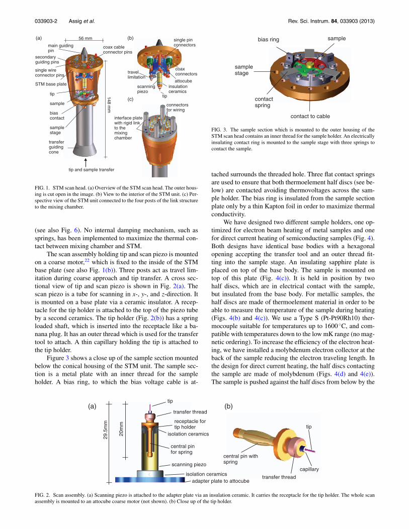
A three-dimensional model of the STM unit is shownin Fig. 1(a). It consists of the STM base plate, the scan as-sembly, a conical housing (with a cross sectional view to re-veal the inside), the sample section at the bottom, and thetransfer guiding cone. The STM has been constructed fromoxygen-free, high conductivity copper (OFHC) and coin sil-ver, which is a 93.5% Ag and 6.5% Cu alloy. The copper partsare gold plated, without using a Ni wetting layer in between.Aluminum nitride (Shapal M) or crystalline aluminum oxide(sapphire) have been used as insulating materials. The trans-fer guiding cone, aligning the axes of the transfer tool and theSTM unit, is made of Ti reducing its total weight. For gluingUHV compatible components, electrically insulating epoxyhas been used.
The STM unit is assembled on the base plate shown inFig. 1(b). All electrical connections are interfaced at this platewith home built single wire and coaxial connectors allowingfast and easy exchange of scan heads. For this reason guidingpins are mounted on top of the base plate so that the completeSTM head can be exchanged blindly without disassemblingthe cryostat. The scan assembly and the conical housing (notshown in Fig. 1(b)) are attached to the base plate. The conicalhousing has been optimized in design so that the response ofthe tip-sample distance to external vibrations is minimized.21
In Fig. 1(c) the interface plate is shown, to which theSTM base plate is connected. Four rods, along which thewiring is guided to the interface plate, extend rigidly fromthe center of the magnetic field, where the STM is located,to the mixing chamber, which is the cold spot of the cryostat
0034-6748/2013/84(3)/033903/9/$30.00 © 2013 American Institute of Physics84, 033903-1
033903-2 Assig et al. Rev. Sci. Instrum. 84, 033903 (2013)
main guidingpin
tip
STM base plate
single wireconnector pins
secondaryguiding pins
coax cableconnector pins
transferguidingcone
sample
56 mm
148m
m
biascontact
tip and sample transfer
tip
insulationceramics
travellimitation
attocube
coaxconnectors
scanningpiezo
single pinconnectors
(a () b)
(c)
samplestage
interface platewith rigid linkto themixingchamber
connectorsfor wiring
FIG. 1. STM scan head. (a) Overview of the STM scan head. The outer hous-ing is cut open in the image. (b) View to the interior of the STM unit. (c) Per-spective view of the STM unit connected to the four posts of the link structureto the mixing chamber.
(see also Fig. 6). No internal damping mechanism, such assprings, has been implemented to maximize the thermal con-tact between mixing chamber and STM.
The scan assembly holding tip and scan piezo is mountedon a coarse motor,22 which is fixed to the inside of the STMbase plate (see also Fig. 1(b)). Three posts act as travel lim-itation during coarse approach and tip transfer. A cross sec-tional view of tip and scan piezo is shown in Fig. 2(a). Thescan piezo is a tube for scanning in x-, y-, and z-direction. Itis mounted on a base plate via a ceramic insulator. A recep-tacle for the tip holder is attached to the top of the piezo tubeby a second ceramics. The tip holder (Fig. 2(b)) has a springloaded shaft, which is inserted into the receptacle like a ba-nana plug. It has an outer thread which is used for the transfertool to attach. A thin capillary holding the tip is attached tothe tip holder.
Figure 3 shows a close up of the sample section mountedbelow the conical housing of the STM unit. The sample sec-tion is a metal plate with an inner thread for the sampleholder. A bias ring, to which the bias voltage cable is at-
samplestage
contactspring
bias ring
contact to cable
sample
FIG. 3. The sample section which is mounted to the outer housing of theSTM scan head contains an inner thread for the sample holder. An electricallyinsulating contact ring is mounted to the sample stage with three springs tocontact the sample.
tached surrounds the threaded hole. Three flat contact springsare used to ensure that both thermoelement half discs (see be-low) are contacted avoiding thermovoltages across the sam-ple holder. The bias ring is insulated from the sample sectionplate only by a thin Kapton foil in order to maximize thermalconductivity.
We have designed two different sample holders, one op-timized for electron beam heating of metal samples and onefor direct current heating of semiconducting samples (Fig. 4).Both designs have identical base bodies with a hexagonalopening accepting the transfer tool and an outer thread fit-ting into the sample stage. An insulating sapphire plate isplaced on top of the base body. The sample is mounted ontop of this plate (Fig. 4(c)). It is held in position by twohalf discs, which are in electrical contact with the sample,but insulated from the base body. For metallic samples, thehalf discs are made of thermoelement material in order to beable to measure the temperature of the sample during heating(Figs. 4(b) and 4(c)). We use a Type S (Pt-Pt90Rh10) ther-mocouple suitable for temperatures up to 1600 ◦C, and com-patible with temperatures down to the low mK range (no mag-netic ordering). To increase the efficiency of the electron heat-ing, we have installed a molybdenum electron collector at theback of the sample reducing the electron traveling length. Inthe design for direct current heating, the half discs contactingthe sample are made of molybdenum (Figs. 4(d) and 4(e)).The sample is pushed against the half discs from below by the
tip
transfer thread
central pin withspring
(a) (b)
capillary
tip
transfer thread
central pinfor spring
isolation ceramics
receptacle fortip holder
scanning piezo
isolation ceramicsadapter plate to attocube
29.5
mm
20m
m
FIG. 2. Scan assembly. (a) Scanning piezo is attached to the adapter plate via an insulation ceramic. It carries the receptacle for the tip holder. The whole scanassembly is mounted to an attocube coarse motor (not shown). (b) Close up of the tip holder.

033903-3 Assig et al. Rev. Sci. Instrum. 84, 033903 (2013)
(a)
(d) (e)
(b) (c)thermocouplehalf discs
half discs
base body
sample
insulationceramics
screw forclamping
e-beamcollector
insulationceramics
base body
sample
isolationceramics
spacerplates
22 mm
13 mm
FIG. 4. Sample holder. (a) Completely assembled sample holder for e-beamheating. The base of the sample holder is a body containing an outer threadfitting into the sample section. An e-beam collector and the sample areclamped to the base body by two half discs made of thermoelement material.(b) One half disc is removed. A sapphire plate is used to insulate the sam-ple and e-beam collector from the base body. (c) Cross section through thesample holder. (d) Perspective view of the sample holder adapted for semi-conducting samples. The half discs fixing the sample to the base body aremade of molybdenum. (e) Spacer platelets compensate for different waferthickness.
spring force of small spacer platelets in order to allow for thesample to thermally expand reducing the risk of deformation.
Tips and samples are transferred through the bottom ofthe cryostat. This greatly reduces the transfer length as op-posed to a top loading design. Due to the geometry of thecryostat there is no visual access to the scan head during thetransfer procedure. To ensure a safe transfer, two PEEK align-ment rings center the axis of the transfer tool into the transfercone of the STM unit. Solid state joints below the alignmentrings (not shown) capable of transferring torque, but other-wise flexible can compensate a small misalignment. The headof the transfer tool has the shape of an Allen key, fitting intothe back of the sample (see Fig. 5(b)). The head has a threadedhole to accept the tip holder (see Fig. 5(c)). The tip apex is in-side this threaded hole, so that it is optimally protected duringthe transfer procedure.
outerhousing
transferguiding cone
transfertool
ring foralignment
Allen keyfor sample
tip
sample
(a) (b) (c)
sample
tip holder
threadedhole for tip
FIG. 5. Tip and sample transfer. (a) The transfer tool is moved into the STMunit through the guiding cone. The transfer head is an Allen key fitting intothe back of the sample holder. A threaded hole on top is used for accepting thetip holder. Two alignment rings slide into the transfer guiding cone ensuringalignment of the axes. (b) The sample is transferred to the STM. (c) The tipis removed from the STM.
outer vacuumshell
feedthrough forwires going into theUHV space
liquid nitrogenreservoir
liquid heliumreservoir
still pumping line
inner vacuumflange
1K-Pot
still chamber
magnet system
shutterfeedthroughs
UHV flange toexperimental chamber
mixing chamber
STM unit
link structure
4.2K radiationshutter
77K radiationshutter
heat exchangers
0.8K radiationshutter
FIG. 6. Cross sectional view through the complete cryostat.
III. THE DILUTION REFRIGERATOR
Generating temperatures continuously below 100 mKwith high cooling power requires dilution refrigeration.23, 24
The refrigerant is a 3He/4He mixture which starts to separateinto two phases at temperatures below 800 mK: a concen-trated (3He rich) and a diluted (4He rich) phase. The coolingprocess relies on the different enthalpy for 3He atoms withinthe two phases. The phase separation as well as the coolingtakes place in the mixing chamber (MC), which is the coldestspot in the dilution refrigerator. A technical realization of di-lution refrigeration was first reported by Das et al. in 1965.25
Reviews on the theoretical and technical aspects can be foundin Refs. 26–30.
A cut through our dilution refrigerator, which is a customdesigned model fabricated by Janis Research Company,31 isshown in Fig. 6. The cryostat is UHV compatible with liquidnitrogen (LN2) and liquid helium (LHe) reservoirs acting asthermal radiation shields. The whole cryostat can be baked to100 ◦C limited by the materials used in the magnet design.A solenoid magnet, a saddle coil, as well as a compensationcoil are welded into the LHe reservoir. Magnetic fields up to14 T (0.5 T) can be generated perpendicular (in one directionparallel) to the sample surface. At the same time we can com-pensate the large stray fields of the solenoid magnet in the

033903-4 Assig et al. Rev. Sci. Instrum. 84, 033903 (2013)
region of the MC. The dilution unit is mounted to the UHVside of the inner vacuum flange above the magnet (see Fig. 6).All pipes for the operation of the dilution cycle as well as ca-bles for cryostat and STM operation are fed through the innervacuum flange (not shown).
The dilution unit consists of a 1K pre-cooling stagein combination with the condenser impedance (Z = 3× 1010 cm−3), a still chamber, where the fluid level of thediluted phase is located, and a heat exchanger section withthe mixing chamber, below which the link structure and theSTM are mounted (Fig. 6). The 1K pre-cooling stage con-sists of a large volume 1K-pot with an acoustic noise reducer.The noise reducer is intended to condense any gas bubble,which may occur during liquid 4He expansion, before thebubble could enter the 1K-pot volume (whistle effect). In thisway, we are able to leave the 1K-pot running during measure-ments. To minimize heat input from thermal radiation, the MCand STM are protected by radiation shields anchored at theLN2-reservoir (77 K), the LHe-reservoir (4 K), and the stillchamber (800 mK). Access through the radiation shields fortip and sample transfer is given by shutter mechanisms. TheUHV preparation chamber connects to the bottom flange ofthe cryostat.
Temperature measurements are performed using resistiveand magnetic thermometry.32 The resistive temperature sen-sors are based on ruthenium oxide (RuO) clusters in a glassmatrix.33–36 While the RuO sensors are the workhorse in rou-tine cryostat operation down to 30 mK,37 the lower tempera-tures of the mixing chamber require sensors less susceptibleto saturation effects. Janis Research Company provides a so-lution with a pair of mutual inductance sensors.38 The sus-ceptibility of a paramagnetic cerium magnesium nitrate salt(CMN) follows the Curie-Weiss law with 5% accuracy downto about 5 mK.27, 39 The corresponding fitting function con-tains only two fitting parameters. These are obtained from theknown superconducting transition temperatures (see Table I)in a Fixed Point Device (FPD), where different seeds of super-conducting compounds are compressed into silver powder. Inthe FPD, the transitions are seen as jumps in the mutual induc-tance due to the Meissner effect. A typical calibration curve isshown in Fig. 7, where the black line is the Curie-Weiss lawused to interpolate and extrapolate the scale for a continuoustemperature reading from 1 K down to about 8 mK. The typ-ical relaxation time of the CMN sensor is about 150 s near10 mK.
Different RuO temperature sensors are positioned at var-ious temperature levels of the dilution stage (at the 1K-potlevel, still chamber, heat exchanger section, MC and STM
TABLE I. Some of the superconducting compounds and the correspondingsuperconducting transition temperatures in the FPD temperature sensor.
Superconducting Transitionimpurity temperature (mK)
Cd 520AuIn2 208AuAl2 161Ir 96
-4.00
-3.99
-3.98
-3.97
-3.96
-3.95
Mut
ual I
nduc
tanc
e C
MN
(m
H)
10x10-38642
1/T (1/mK)
AuIn2-point
AuAl2-point
Cd-point
Ir-point
FIG. 7. Calibration curve of the CMN magnetization thermometer. Magne-tization values are plotted against the inverse transition temperature of thesuperconducting compounds in the fixed point device (see text for details).
support). In the RuO sensor, the electron transport is dueto thermally activated electrons, which hop between energystates localized at the RuO clusters near the Fermi level (Motthopping). We calibrate the RuO temperature sensor at MC andSTM support against the CMN temperature sensor.40 In thisway, we get a set of temperature (T) and resistance (R) valueswhich are expected to follow the Mott hopping law41
σ = 1
R= A0 exp
[−
(A1
T
)γ ], (1)
where A0 is a scaling factor, A1 depends on the DOS nearthe Fermi level as well as the decay length of the wave func-tions of the localized states. The temperature exponent γ isexpected to be 1/2 for pure Mott hopping. However, includ-ing Coulomb interaction results in γ ≈ 1/4 (Efros-Shklovskiihopping).42 At very low temperatures the resistance curvesof the temperature sensors deviate from the standard Mottmodel. To account for these deviations we use a phenomeno-logical extension to the above formula:
σ = 1
R= A0 exp
[−
(A1
T − T0
)γ ]+ σ0. (2)
Here, σ 0 is a temperature independent conductivity, whichis attributed to percolation paths within the glass matrix andtemperature independent tunneling. The value T0 is used todescribe a faster saturation of the conductivity than suggestedby the Mott hopping law. It is not to be regarded as an ex-perimental offset to compensate for calibration errors. Thesaturation can be physically motivated by additional localiza-tion effects at low temperatures (e.g., Anderson localization).However, we also found that the parameters σ 0 and T0 de-pend on the local environment, in which the sensor is located.In Fig. 8(a) the obtained resistance values are plotted againstthe MC temperature which is measured by the CMN temper-ature sensor. The black lines are the fit to the data using theinverse function of Eq. (2), i.e., T(R). The relative deviationbetween fit and measured temperature is shown in Fig. 8(b).The fit coefficients are summarized in Table II. It turns outthat the modified Mott hopping law with the two additionalparameters yields a much better agreement with the data inthe temperature region below 35 mK.

033903-5 Assig et al. Rev. Sci. Instrum. 84, 033903 (2013)
TABLE II. Fitting coefficients for the temperature calibration of the resistive temperature sensors at MC and STM support.
Sensor A0 × 10−3 (�−1) A1 × 103 (mK) γ σ 0 × 10−6 (�−1) T0 (mK)
MC 8.1 ± 0.1 64.7 ± 0.5 0.258 ± 0.001 1.04 ± 0.03 11.8 ± 0.4STM support 6.0 ± 0.1 30.6 ± 0.5 0.283 ± 0.001 1.70 ± 0.03 9.6 ± 0.4
The cryostat performance is characterized by its basetemperature and cooling power Q. In a dilution cryostat thelatter depends on the 3He circulation n.19, 26, 27 Heating the stillchamber increases n, which increases Q resulting in a lowerMC temperature26, 27 until the heat load from the 3He input be-comes too high and the MC temperature increases again. Op-timum circulation is achieved when these two contributionsare in balance. The MC temperature of our cryostat as a func-tion of the 3He circulation n shown in Fig. 9 indicates a clearminimum. Fitting with a second order polynomial, we findthat the optimal circulation is n = 160 ± 1 μmol/s at whichwe reach a base temperature of 11.4 ± 0.3 mK. The coolingpower of our cryostat at 100 mK, which we determined bymeasuring the heater power needed to stabilize the MC at thistemperature, is 396 ± 5 μW.
IV. IMPLEMENTATION OF THE mK-STM
Concerning the wiring of cryostat and STM, eighteen un-shielded wires in twisted pair configuration and three shieldedcables (for bias voltage, tunneling current and z-signal of thescan tube) are connected to the STM unit. Care was taken notto interrupt the shielding of the coaxial cables at any pointdown to the STM to reduced the noise pick-up for the mostsensitive signals. Low thermal conductivity materials havebeen used for cables and wires from room temperature tothe MC to minimize the heat load. In our system, we use
2
3
456
100
2
3
456
1000
Tem
pera
ture
(m
K)
3 4 5 6 7 810
4
2 3 4 5 6 7 810
5
2 3 4 5 6 7 8
-15
-10
-5
0
5
10
Dev
iatio
n (%
)
3 4 5 6 7 8
104
2 3 4 5 6 7 8
105
2 3 4 5 6 7 8
Resistance (Ω)
(a)
(b)
FIG. 8. Calibration curves of the RuO temperature sensors. (a) Temperaturecalibration curves. Red: data from RuO sensor at MC, blue: data for RuOsensor at the interface plate, black: fit to the data. (b) Relative deviationsbetween fitting curves and measured data. The fits lie very well on the databelow 500 mK with less than 5% of error.
stainless steel coaxial cables and manganine (Cu86Mn12Ni2)twisted pair wires. The only exception to the wiring schemementioned above are the electrical connections to the coarsemotor. In order to keep the rising edge of the signal for theslip-stick motion as steep as possible, the total resistance forthe coarse motor wires should not exceed 10 �. Therefore,we use thin copper wires from room temperature to the 1 Kpot stage and proceed with superconducting wires to blockheat transport along these lines to the MC. All cables are ther-mally anchored at every stage down to the MC. From the MCto the STM high thermal conductivity is desired. For the un-shielded wires we use Kapton insulated silver wires. For theshielded cables we use semi-rigid copper cables in the supportstructure and coaxial cables with copper inner conductor anda gold plated copper braid within the STM scan head.
To avoid ground loops, we have chosen the cryostat to bethe common grounding point. We took care to electrically iso-late it from the environment, so that the cryostat is completelyelectrically floating except for one low resistance connectionto ground. To avoid high frequency pick-up, all lines enteringthe cryostat are electrically filtered at the room temperaturefeedthroughs by commercially available π -filters43, 44 in se-ries with a resistor to achieve a cut-off frequency of 10 kHz.Within the cryostat, no internal cryogenic filters are used otherthan the intrinsic distributed RC-filters of the coaxial cables.
The UHV preparation chamber is mounted to the bottomflange of the cryostat. It allows standard UHV preparationlike sputtering, sample annealing, deposition of materials, andUHV cleaving. A load-lock attached to the UHV chamber al-lows to transfer samples, tips and filament units (see below)from ambient conditions into UHV. Along with the two dif-ferent designs of the sample holders mentioned above, wedeveloped two sample preparation stages, one for electron
17
16
15
14
13
12
Tem
pera
ture
(m
K)
25020015010050 Flow (µmole/s)
FIG. 9. MC temperature as a function of the 3He circulation. There is a clearminimum for circulation rates between about 130 μmol/s and 200 μmol/s.The cryostat is normally operated at lowest circulation rate at a temperatureof about 15 mK.
033903-6 Assig et al. Rev. Sci. Instrum. 84, 033903 (2013)
(a) (b)
(c)
(d)
(e)
metal stripsfor samplecontact
link tomanipulator
isolatedconnectorfor filament
transferrable filamentin parking position
electrically isolatedmanipulator head
filamenttransferred tooperatingposition
positions for additionaltip storage
direct currentheating forsemiconductingsamples
60.5 mm
12 mm
Wehnelt cylinder
filament wire
filament contact
tip storage
tip holder
contact for directcurrent heating
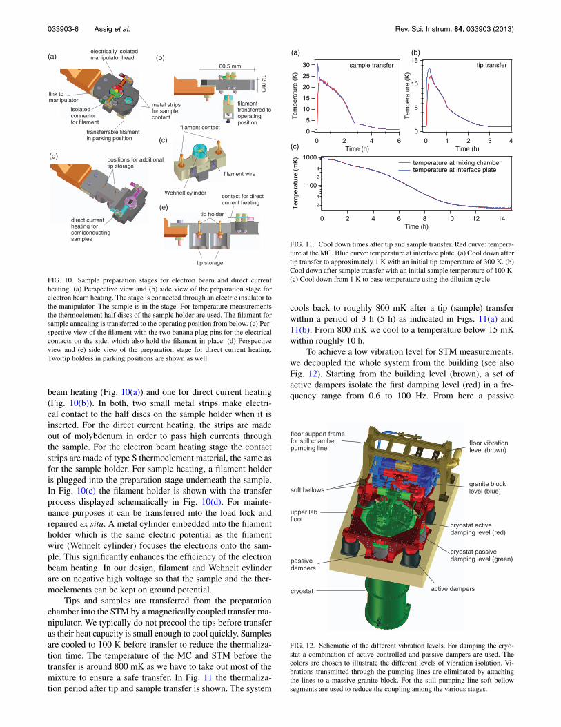
FIG. 10. Sample preparation stages for electron beam and direct currentheating. (a) Perspective view and (b) side view of the preparation stage forelectron beam heating. The stage is connected through an electric insulator tothe manipulator. The sample is in the stage. For temperature measurementsthe thermoelement half discs of the sample holder are used. The filament forsample annealing is transferred to the operating position from below. (c) Per-spective view of the filament with the two banana plug pins for the electricalcontacts on the side, which also hold the filament in place. (d) Perspectiveview and (e) side view of the preparation stage for direct current heating.Two tip holders in parking positions are shown as well.
beam heating (Fig. 10(a)) and one for direct current heating(Fig. 10(b)). In both, two small metal strips make electri-cal contact to the half discs on the sample holder when it isinserted. For the direct current heating, the strips are madeout of molybdenum in order to pass high currents throughthe sample. For the electron beam heating stage the contactstrips are made of type S thermoelement material, the same asfor the sample holder. For sample heating, a filament holderis plugged into the preparation stage underneath the sample.In Fig. 10(c) the filament holder is shown with the transferprocess displayed schematically in Fig. 10(d). For mainte-nance purposes it can be transferred into the load lock andrepaired ex situ. A metal cylinder embedded into the filamentholder which is the same electric potential as the filamentwire (Wehnelt cylinder) focuses the electrons onto the sam-ple. This significantly enhances the efficiency of the electronbeam heating. In our design, filament and Wehnelt cylinderare on negative high voltage so that the sample and the ther-moelements can be kept on ground potential.
Tips and samples are transferred from the preparationchamber into the STM by a magnetically coupled transfer ma-nipulator. We typically do not precool the tips before transferas their heat capacity is small enough to cool quickly. Samplesare cooled to 100 K before transfer to reduce the thermaliza-tion time. The temperature of the MC and STM before thetransfer is around 800 mK as we have to take out most of themixture to ensure a safe transfer. In Fig. 11 the thermaliza-tion period after tip and sample transfer is shown. The system
15
10
5
0
Tem
pera
ture
(K
)
43210Time (h)
tip transfer30
25
20
15
10
5
0
Tem
pera
ture
(K
)
6420Time (h)
sample transfer
2
4
1002
4
1000
Tem
pera
ture
(m
K)
14121086420Time (h)
temperature at mixing chamber temperature at interface plate
(a) (b)
(c)
FIG. 11. Cool down times after tip and sample transfer. Red curve: tempera-ture at the MC. Blue curve: temperature at interface plate. (a) Cool down aftertip transfer to approximately 1 K with an initial tip temperature of 300 K. (b)Cool down after sample transfer with an initial sample temperature of 100 K.(c) Cool down from 1 K to base temperature using the dilution cycle.
cools back to roughly 800 mK after a tip (sample) transferwithin a period of 3 h (5 h) as indicated in Figs. 11(a) and11(b). From 800 mK we cool to a temperature below 15 mKwithin roughly 10 h.
To achieve a low vibration level for STM measurements,we decoupled the whole system from the building (see alsoFig. 12). Starting from the building level (brown), a set ofactive dampers isolate the first damping level (red) in a fre-quency range from 0.6 to 100 Hz. From here a passive
active dampers
passivedampers
cryostat
upper labfloor
soft bellows
floor support framefor still chamberpumping line
floor vibrationlevel (brown)
granite blocklevel (blue)
cryostat activedamping level (red)
cryostat passivedamping level (green)
FIG. 12. Schematic of the different vibration levels. For damping the cryo-stat a combination of active controlled and passive dampers are used. Thecolors are chosen to illustrate the different levels of vibration isolation. Vi-brations transmitted through the pumping lines are eliminated by attachingthe lines to a massive granite block. For the still pumping line soft bellowsegments are used to reduce the coupling among the various stages.

033903-7 Assig et al. Rev. Sci. Instrum. 84, 033903 (2013)
upper level lab
separated roomfor pumps
lower level lab
cryostat
vibration isolationfor cryostat
vibration isolationfor pumping lines
UHV preparationchamber
gas handlingsystem
FIG. 13. Overview of the mK-STM setup. The cryostat rests on a vibra-tion isolation stage in the upper level lab. It hangs through the ceiling intothe lower level lab with the UHV preparation chamber attached at the bot-tom. The pumps are located in a separate room hanging from the ceiling toavoid mechanical disturbances on the floor, on which the vibration isolationis placed.
damping stage decouples the cryostat (green). To reduce thevibrational noise of the 1 K-pot-, nitrogen- and dilution cycle-pumps, we used flexible hoses for the connections to the cryo-stat. All pumping lines and cables are fixed on a heavy graniteblock (blue), which itself is isolated from the floor with activedampers, before going to the cryostat. For the still pumpingline, which has the largest diameter (100 mm), soft bellowswere arranged in an opposing configuration in order to com-pensate the vacuum forces, when crossing over the differentdamping stages (see Fig. 12).45 All pumps are placed in a sep-arated acoustically shielded room.
An overview of the complete setup is depicted in Fig. 13.The cryostat including the UHV chamber is supported at thefloor of the upper level lab. From this lab, we handle cryostatand STM. The UHV preparation chamber is accessible fromthe lab below. Tips and samples are transferred from here aswell.
V. PERFORMANCE
To verify the stability of our STM, we performed topo-graphic measurements at temperatures of 800 mK and 15 mK(MC temperature). An Au(111) surface measured at 800 mK
4.0nm
9.0Å
(a)
(b)
FIG. 14. (a) Topography of Au(111) measured at T = 800 mK. (b) Topog-raphy of Cu(111) with standing wave pattern of the scattered surface statemeasured at T = 15 mK. V = 50 mV, I = 50 pA.
is shown in Fig. 14(a). The noise level can be seen in theline profiles across the image, from which we estimated thenoise in the z-direction to be about 3 pm. The averaging timeper data point during this measurement was 4.2 ms. For lowertemperatures, we operate the 3He flow at the lowest circula-tion rate resulting in a MC temperature of 15 mK. The 1K-potwas running during all measurements. Figure 14(b) shows aCu(111) surface measured at this temperature. In the image,the standing wave pattern of the Cu(111) surface state scat-tered from impurities can be seen. Here, we find a z-noise of4.2 ± 0.5 pm for an averaging time of 3.5 ms per data point.
To verify the temperature of tip and sample, we have tem-porarily modified the setup and installed two RuO tempera-ture sensors at the corresponding positions (see Fig. 15). Weadjusted the MC temperature of the cryostat to 15 ± 0.5 mKhaving a 3He flow rate of 43 μmol/s. Under these conditionswe measured a temperature of 17 ± 5 mK at the tip and
50
40
30
20
Tem
pera
ture
(m
K)
7654321Time (h)
f = 30Hz
f = 15Hz
f = 5Hzf = 1.5Hz
f = 0.5Hz
FIG. 15. Temperature measured directly at tip and sample position of theSTM. The blue graph shows the sample temperature. The red graph shows thetip temperature. The tip slightly warms up when a sine voltage (VPP = 5 V)is applied to the scanning piezo.

033903-8 Assig et al. Rev. Sci. Instrum. 84, 033903 (2013)
160150140130120 Bias Voltage (µV)
Data Fit to Data Fixed Teff = 0 mK Fixed Teff = 30 mK Fixed Teff = 50 mK Fixed Teff = 60 mK
2.0
1.5
1.0
0.5
0.0
Diff
eren
tial C
ondu
ctan
ce (
arb.
uni
ts)
-400 -200 0 200 400Bias Voltage (µV)
(a)
(b)0.3
0.2
0.1
0.0
Diff
. Con
duct
ance
(ar
b. u
nits
)
-160 -150 -140 -130 -120 Bias Voltage (µV)
FIG. 16. Measurement of the tunneling conductance between a supercon-ducting Al tip and a Cu(111) surface. (a) The conductance spectrum is shownin red and the fit to the Maki equation is shown in blue. For comparison, a fitat 0 mK is shown in green. (b) Zoom into the corners of the gap. The 0 mKspectrum illustrates that the rounding of the corner is only due to an effectivethermal broadening. For comparison, the dotted spectra show a fit to the datafor different effective temperatures demonstrating the sensitivity of the fit.
20 ± 5 mK at the sample position using the temperature cal-ibration obtained for the RuO temperature sensors when po-sitioned at the MC. In this context, it should be emphasizedagain that below about 35 mK the RuO sensor calibration ishighly sensitive to the local environment even when the sen-sor is just moved from the MC to the tip or sample position.The estimated error above accounts for this uncertainty. Inthis configuration, we checked the temperature evolution dur-ing a simulated scan by applying a 5 Vpp sine-signal to thez-electrode of the scanning piezo equivalent to a tip displace-ment of 2 nm perpendicular to the sample surface. Using afrequency of 30 Hz, we observed an increase in the tip tem-perature to about 55 mK, due to the heat released from thescanning piezo. Decreasing the frequency in steps resulted ina stepwise lowering of the tip temperature. The sample tem-perature stayed constant during this experiment showing thatthe heat generated by the piezo does not affect the sample.
To verify the energy resolution of the STM, we measurethe superconducting gap of aluminum.46 Aluminum is ideallysuited because it is a weakly coupling superconductor witha nearly isotropic gap.47–49 Therefore, we expect broadeningeffects to be mainly due to the finite temperature of the nor-mal conducting Cu(111) sample as well as the experimentalbroadening.
We prepare our Al tips from high purity Al wire hav-ing a diameter of 0.25 mm. The tips are cut under ambientconditions and immediately transferred into vacuum. The ox-ide layer is removed by Ar ion sputtering without further an-
TABLE III. Fitting coefficients of the tunneling conductance between an Altip and a Cu(111) surface. The DOS was calculated using the Maki equationwhich is explained in the text. Here � is the superconducting gap, ξ is thepair-braking parameter originating from the Maki theory, and T is the effec-tive temperature. The energy resolution �E = 3.5kBTeff has been calculatedfrom the effective temperature.
� (μeV) ζ Teff (mK) �E (μeV)
183.3 ± 0.1 0.023 ± 0.001 38 ± 1 11.4 ± 0.3
nealing. If necessary, we have used field emission treatmentsfor further modification of the tip. Tunneling spectroscopymeasurements were done on a Cu(111) surface, which wascleaned by cycles of Ar ion sputtering and annealing. Arepresentative measurement at TMC = 15 mK is shown inFig. 16(a). With a superconducting transition temperature ofTC = 1.2 K, the conductance spectrum shows a fully devel-oped gap at 15 mK with a value of � = 183.3 μeV. All elec-trons at the Fermi level are condensed in the BCS groundstate.
To describe the DOS of the superconducting tip we haveused the Maki equation.50 Spin-orbit scattering effects cancelout as we do not apply any magnetic field (see the Appendixand Ref. 51). The orbital pair breaking parameter ζ reducesthe singularities in the coherence peaks to finite values, butmaintains a sharp edge in the corners of the gap. The ther-mal broadening of the measured conductance spectra is ac-counted for by a convolution of the Maki equation with thederivative of the Fermi-Dirac distribution of the metal sub-strate. This means that the only rounding of the corner in thegap is due to thermal broadening. Other contributions, suchas experimental broadening, noise, or the gap anisotropy, willhave a similar effect on the spectrum as the thermal broad-ening. Therefore, we regard the temperature parameter in thisfit function as an effective temperature. It gives an estimateof the upper limit for the energy resolution. The resulting fitfunction is superimposed onto the conductance spectrum inFig. 16(a) (blue line). The fitting parameters are summarizedin Table III. From the fit we find an effective temperature ofT = 38 ± 1 mK corresponding to an energy resolution of�E = 3.5kBTeff = 11.4 ± 0.3 μeV. To better show the qual-ity of the agreement, the corners of the gap are magnified inFig. 16(b). The rounding of the corners can clearly be at-tributed to the effective thermal and experimental broadeningas the corner becomes sharp at 0 mK (green line). Differentfits (dotted lines), where the effective temperature was heldfixed at values between 30 mK and 60 mK demonstrate thesensitivity of the fit function to changes in the effective tem-perature. We would like to point out that no internal cryogenicsignal filtering has been implemented.
VI. CONCLUSION
We have presented the design and performance of anSTM operating at temperatures of 10 mK. This is realized byattaching the STM unit to a dilution cryostat. Tips and sam-ples can be transferred in situ from the UHV chamber intothe STM. In this setup, we can apply high magnetic fields of

033903-9 Assig et al. Rev. Sci. Instrum. 84, 033903 (2013)
14 T perpendicular and 0.5 T parallel to the sample surface.We estimated the electronic resolution by analyzing tunnelingspectra between a superconducting Al tip and a normal metalsample resulting in an energy resolution of 11.4 μeV. In thisway, the lowest possible energy scales, such as the Zeemansplitting or the hyperfine splitting, become observable. Thisopens up exciting new possibilities for spectroscopy on a lo-cal scale.
ACKNOWLEDGMENTS
We gratefully acknowledge the technical supportthroughout the construction phase by A. Koch and P. Andleras well as fruitful discussions with V. Shvarts and Z. Zhao.C.R.A. acknowledges funding from the Emmy-Noether-Program of the Deutsche Forschungsgemeinschaft (DFG).
APPENDIX: SIMPLIFIED MAKI-EQUATION
We used the Maki formalism to calculate the supercon-ducting quasiparticle DOS.50, 51 Without an external magneticfield the DOS ρ(E) reduces to
ρ(E) = Re
(u√
u2 − 1
)(A1)
with u defined by the following nonlinear equation:
u = E
�+ ζ
u√1 − u2
. (A2)
The quantity ζ is the pair breaking parameter. It is possi-ble to solve Eq. (A2) analytically
u = 1
2
(|ε|+
√1−ζ 2+d+
√1+ε2−ζ 2−d−2|ε|(1+ζ 2)√
1−ζ 2+d
),
(A3)
where the following abbreviations are used
ε = E
�,
b = ε2 + ζ 2 − 1,
c = 108ε2ζ 2 + 2b3 +√
(108ε2ζ 2 + 2b3)2 − 4b6,
d = b
3+ 21/3b2
3c1/3+ c1/3
3 · 21/3.
Convolving Eq. (A1) with the Fermi function derivativeyields the fit function.
1G. Binnig, H. Rohrer, C. Gerber, and E. Weibel, Appl. Phys. Lett. 40, 178(1982).
2G. Binnig, H. Rohrer, C. Gerber, and E. Weibel, Phys. Rev. Lett. 49, 57(1982).
3G. Binnig, H. Rohrer, C. Gerber, and E. Weibel, Phys. Rev. Lett. 50, 120(1983).
4A. Richardella, P. Roushan, S. Mack, B. Zhou, D. A. Huse, D. D.Awschalom, and A. Yazdani, Science 327, 665 (2010).
5K. J. Franke, G. Schulze, and J. I. Pascual, Science 332, 940 (2011).6S. Loth, S. Baumann, C. P. Lutz, D. M. Eigler, and A. J. Heinrich, Science335, 196 (2012).
7M. F. Crommie, C. P. Lutz, and D. M. Eigler, Nature (London) 363, 524(1993).
8C. J. Chen, Introduction to Scanning Tunneling Microscopy (Oxford Uni-versity Press, 1993).
9L. Diekhöner, M. A. Schneider, A. N. Baranov, V. S. Stepanyuk, P. Bruno,and K. Kern, Phys. Rev. Lett. 90, 236801 (2003).
10D. Vion, P. F. Orfila, P. Joyez, D. Esteve, and M. H. Devoret, J. Appl. Phys.77, 2519 (1995).
11F. Delgado and J. Fernandez-Rossier, Phys. Rev. Lett. 107, 076804 (2011).12R. Meservey, P. M. Tedrow, and P. Fulde, Phys. Rev. Lett. 25, 1270 (1970).13P. M. Tedrow and R. Meservey, Phys. Rev. Lett. 26, 192 (1971).14P. Fulde, Adv. Phys. 22, 667 (1973).15N. Moussy, H. Courtois, and B. Pannetier, Rev. Sci. Instrum. 72, 128
(2001).16H. Suderow, I. Guillamon, and S. Vieira, Rev. Sci. Instrum. 82, 033711
(2011).17M. Marz, G. Goll, and H. v. Löhneysen, Rev. Sci. Instrum. 81, 045102
(2010).18T. Matsui, H. Kambara, and H. Fukujama, J. Low Temp. Phys. 121, 803
(2000).19Y. J. Song, A. F. Otte, V. Shvarts, Z. Zhao, Y. Kuk, S. R. Blankenship, A.
Band, F. M. Hess, and J. A. Stroscio, Rev. Sci. Instrum. 81, 121101 (2010).20M. Assig, “Development of a Millikelvin scanning tunneling microscope
for applications in ultra high vacuum and high magnetic fields (No 5204),”Ph.D. dissertation, École Polytechnique Fédérale de Lausanne, 2011.
21C. R. Ast, M. Assig, A. Ast, and K. Kern, Rev. Sci. Instrum. 79, 093704(2008).
22attocube systems AG. ANPz50/LT/UHV z-positioner.23H. London, in Proceedings of International Conference on Low Temper-
ature Physics (International Union of Pure and Applied Physics, Oxford,UK, 1951), p. 157.
24H. London, G. R. Clarke, and E. Mendoza, Phys. Rev. 128, 1992 (1962).25T. P. Das, R. de Bruyn Ouboter, and K. W. Taconis, in Proceedings of
9th International Conference on Low Temperature Physics (Plenum Press,1965), p. 1253.
26O. V. Lounasmaa, Experimental Principles and Methods Below 1K (Aca-demic Press Inc., 1974).
27F. Pobell, Matter and Methods at Low Temperatures, 3rd ed. (Springer,2007).
28J. C. Wheatley, Am. J. Phys. 36, 181 (1968).29J. C. Wheatley, O. E. Vilches, and W. R. Abel, Phys. 4, 1 (1968).30J. C. Wheatley, R. E. Rapp, and R. T. Johnson, J. Low Temp. Phys. 4, 1
(1971).31V. Shvarts, Z. Zhao, L. Bobb, and M. Jirmanus, J. Phys.: Conf. Ser. 150,
012046 (2009).32P. R. N. Childs, J. R. Greenwood, and C. A. Long, Rev. Sci. Instrum. 71,
2959 (2000).33M. Watanabe, M. Morishita, and Y. Ootuka, Cryogenics 41, 143 (2001).34W. Schoepe, Physica B 165, 299 (1990).35M. Affronte, M. Campani, S. Piccinini, M. Tamborin, B. Morten, M. Pru-
denziati, and O. Laborde, J. Low Temp. Phys. 109, 461 (1997).36G. E. Pike and C. H. Seager, J. Appl. Phys. 48, 5152 (1977).37I. Batko, K. Flachbart, M. Somora, and D. Vanicky, Cryogenics 35, 105
(1995).38The inductance is measured with an Agilent 4263B LCR meter. The exci-
tation voltage is 100 mV at a lock-in frequency of 120 Hz.39D. S. Greywall and P. A. Busch, Rev. Sci. Instrum. 60, 471 (1989).40The resistances are measured with the Lakeshore 370S resistance bridge.
The excitation voltages range from 632 μV at the 1 K-pot to 20 μV at themixing chamber. The lock-in frequency is 9.8 Hz.
41S. N. Mott, Conduction in Non-Crystalline Materials (Oxford UniversityPress, 1993).
42A. L. Efros and B. I. Shklovskii, J. Phys. C 8, L49 (1975).43Spectrum control Inc. 51-726-017.44Spectrum control Inc. 1289-004.45W. P. Kirk and M. Twerdochlib, Rev. Sci. Instrum. 49, 765 (1978).46I. Guillamon, H. Suderow, S. Vieira, and P. Rodiere, Physica C 468, 537
(2008).47T. Kiss, T. Yokoya, A. Chainani, S. Shin, T. Hanaguri, M. Nohara, and H.
Takagi, Nat. Phys. 3, 720 (2007).48I. Guillamon, H. Suderow, S. Vieira, L. Cario, P. Diener, and P. Rodiere,
Phys. Rev. Lett. 101, 166407 (2008).49Y. Noat, T. Cren, F. Debontridder, D. Roditchev, W. Sacks, P. Toulemonde,
and A. S. Miguel, Phys. Rev. B 82, 014531 (2010).50K. Maki, Prog. Theor. Phys. 32, 29 (1964).51D. C. Worledge and T. H. Geballe, Phys. Rev. B 62, 447 (2000).