magnetic tamper detection using low-power hall effect … · magnetic tamper detection using...
TRANSCRIPT

DRV5033DRV5033
UCC28910Transformer-
Based FlybackPower Supply
Capacitive Power Supply
(TPS54060)
Load
Phase A Phase
C
Phase B
Neu
tral
+
-Sx, COMx
MSP430F67791A
TOTAL kWh
UART RX
UART TX-
Source From Utility
CT
Phase APha
se B
Phase C
6' Modulator
6' Modulator
6' Modulator
+
+
-
+
-
+
-
+
-
VCCVSS
6' Modulator
+
-
+
-
6' Modulator
¯û
24
IA
IB
IC
VA
VB
VN
VN
VC
VN
IN
Neu
tral
CT
CT
CT
Active Energy Pulse
Reactive Energy Pulse
ISO7320VCCVSS
ISO7321VSS
VCC
TRS3232
TPS70933
RS-232 Connection
DTR
RTS
RGNDRS-232GND(RGND)
RS-232VCC
ISO-DVCC
ISO-GND
ISO-ACTIVEISO-REACTIVE
6' Modulator
6' Modulator
VCCVSS
VSSVCCJumper
Selection
AUXVCC1
DRV5033
DRV5033DRV5033
DRV5033
Status LEDs
VSS
Output
VCC
VSS
VCC
Output
3
3
RTCCAPx
6
Px.v
Px.w
Px.x
Py.w
Py.x
VDSYS
Pz.wPz.x
TI DesignsMagnetic Tamper Detection Using Low-Power Hall EffectSensors
TI Designs Design FeaturesThis design implements a Class 0.2 three-phase • Multiple Omnipolar Hall Sensors Monitor Energyenergy measurement system that detects magnetic Measurement CTs and SMPS Transformers totampering using Hall sensors. The TIDA-00839 detects Detect Magnetic Attacksmagnetic tampering when running from both main and • Sensor BOP = ±6.9 mT, Sensor BRP = ±3.5 mTbackup power sources. This design reduces the
• SMPS or Cap-Drop Power Supply Optionscurrent consumption of the Hall sensors to increase• Support for Backup Power Sourcesbattery life when running from the backup power
source. • Software Power Duty-Cycling Reduces CurrentConsumption per Sensor to < 2 µADesign Resources
• Case Tamper Detection CapabilityDesign Folder • Three-Phase Energy Measurement Exceeds ClassTIDA-00839
0.2 Accuracy Requirements From ANSI and IECDRV5033 Product FolderUCC28910 Product Folder • Option for Programmable Penalty for DetectedTPS54060 Product Folder Magnetic FieldsISO7320 Product Folder • TI Energy Library Firmware Calculates All EnergyTRS3232 Product Folder Measurement Parameters Including Active andTPS70933 Product Folder Reactive Power; Active and Reactive Energy; RootISO7321 Product Folder Mean Square (RMS) Current and Voltage; Power
Factor; and Line FrequencyMSP430F67791A Product Folder
Featured Applications• MeteringASK Our E2E Experts
An IMPORTANT NOTICE at the end of this TI reference design addresses authorized use, intellectual property matters and otherimportant disclaimers and information.
All trademarks are the property of their respective owners.
1TIDUB69–January 2016 Magnetic Tamper Detection Using Low-Power Hall Effect SensorsSubmit Documentation Feedback
Copyright © 2016, Texas Instruments Incorporated

System Description www.ti.com
1 System DescriptionIn an energy measurement system, transformers may be used in the system’s power supply or as thesystem’s current sensors. A disadvantage of using transformers is that magnetic fields could causetransformer cores to saturate, thereby rendering them useless. For a transformer used in a power supply,this may lead to the system being unable to be powered normally. For current transformer current sensorsspecifically, this may prevent properly registering the current drawn by a customer’s load, thereby leadingto undercharging a customer for energy consumption. Due to this magnetic susceptibility of transformers,tamperers may purposely subject a system to a magnet in an attempt to paralyze the system. One way ofaddressing magnetic tampering is to measure the magnetic field and take the necessary actions when ahigh magnetic field is detected.
This design implements an ANSI/IEC Class 0.2 accuracy three-phase energy measurement system thatuses the DRV5033 Hall effect sensors for detecting magnetic tampering. This design is for a three-phaseenergy measurement system, but it can also be scaled down for a single-phase system.
This system uses an energy measurement system on chip (SoC) to sense current and voltage, calculatemetrology parameters, drive a 160-segment LCD, and communicate to a PC GUI through the board’sisolated RS-232 circuitry. As an additional tamper detection feature, this SoC can detect attempts to openthe system’s case to physically tamper with the system.
In this application, whenever there is a detected magnetic field there is an option that would allowpenalizing a customer for this high magnetic field. This penalty is accomplished by calculating metrologyparameters with a large, user-defined current instead of calculating metrology parameters using thecurrent actually sensed.
To deal with the magnetic susceptibility of transformer-based supplies, it is common for energymeasurement systems to use cap-drop supplies that do not use transformers. However, for systems thatdraw a large current from the power supply, using a transformer in the power supply may be unavoidable.This design supports using both a cap-drop or transformer power supply through its TPS54060 capacitive-based power supply and its UCC28910 transformer-based power supply. For the transformer-based powersupply, there are Hall effect sensors near the transformer to detect magnetic tamper attempts near thepower supply transformer. If the transformer is paralyzed by a magnetic tamper event and the main poweris lost, the system can switch to a backup power source to allow the system to still be functional. Since thebackup power source may be a battery, it is important to reduce the current consumption of the Hallsensors to maximize battery life cycle. This current consumption reduction is accomplished by duty cyclingthe power to each Hall sensor as in the white paper Sub-Microamp, Intelligent Hall-Effect Sensing Delivers20-Year Battery Life [1].
In regards to metrology, the software energy library supports calculating various parameters for up tothree-phase energy measurement. The key parameters calculated during energy measurements are: RMScurrent and voltage, active and reactive power and energies, power factor, and frequency. Theseparameters can be viewed either from the calibration GUI or LCD. This design guide has a completemetrology source code provided as a downloadable zip file.
2 Magnetic Tamper Detection Using Low-Power Hall Effect Sensors TIDUB69–January 2016Submit Documentation Feedback
Copyright © 2016, Texas Instruments Incorporated

B (mT)
OUT
BOP (S)BRP (N) BOF
BHYS
BRP (S)BOP (N)
BHYS
www.ti.com System Description
1.1 DRV5033The DRV5033 is a Hall effect sensor that detects magnetic tampering. These sensors are omnipolar, sothey could respond to either the south pole or north pole of a magnet. A strong magnetic field of eitherpolarity causes the output to pull low (operate point, BOP), and a weaker magnetic field causes the outputto release (release point, BRP) , as shown in Figure 1.
Figure 1. DRV5033 Output State
This design uses two sets of three sensors. Because these sensors have an open drain output, theoutputs of the multiple sensors can simply be directly connected to each other. The shared output wouldindicate whether or not a magnetic field is detected on any of the multiple Hall sensors. The first set ofsensors is oriented so that there is one sensor near each current transformer. The second set of threesensors is placed near the power supply transformer (near the center of the board). For this particular setof sensors, each sensor is oriented so that it could sense magnetic tampering in all three dimensions. Forsensing in three dimensions, two SIP package DRV sensors are used with one SOT23 package DRVsensor.
1.2 UCC28910The UCC28910 is used in the transformer-based power supply to help provide a 3.3-V output from aninput mains voltage of 100- to 240-V ACRMS at 50 or 60 Hz. Figure 8 shows how the UCC28910 is used tocreate the 3.3-V output from the 100- to 240-V ACRMS input. To detect a magnetic tamper event near thetransformer in this power supply, a set of three Hall sensors are used (one for each direction).
1.3 TPS54060The TPS54060 is used in the capacitive-based power supply to provide a 3.3-V output from an inputmains voltage of 100- to 240-V ACRMS at 50 or 60 Hz. Figure 7 shows the TPS54060-based power supply,which outputs 3.3-V using a 100- to 240-V ACRMS input.
1.4 ISO7321To add isolation to the RS-232 connection to a PC, the isolated RS-232 portion of this design usescapacitive galvanic isolation, which has an inherent lifespan advantage over an opto-isolator. In particular,industrial devices are usually pressed into service for much longer periods of time than consumerelectronics; therefore, maintenance of effective isolation over a period of 15 years or longer is important.
The TI ISO7321 is a simple dual-channel isolator that is capable of operating at 3.3 V or 5 V, enabling awide range of devices that can connect to the data circuit-terminating equipment (DCE) side of theinterface. The ISO7321 can simply be inserted into a universal asynchronous receiver/transmitter (UART)signal path, with the appropriate power supplies on each side to enable operation. The ISO7321 alsomaintains 3 kV of isolation to meet the Underwriters Laboratories (UL) certification levels.
The ISO7321 is available as ISO7321C and ISO7321FC variants, and the difference of these variants is inwhether the default output is high or low, respectively. Although both variants can be used in the design,this design specifically uses the ISO7321C.
3TIDUB69–January 2016 Magnetic Tamper Detection Using Low-Power Hall Effect SensorsSubmit Documentation Feedback
Copyright © 2016, Texas Instruments Incorporated

System Description www.ti.com
1.5 TRS3232To properly interface with the RS-232 standard, a voltage translation system is required to convertbetween the 3.3-V domain on the board and from the 12 V on the port itself. To facilitate the translation,the design uses the TRS3232. The TRS3232 is capable of driving the higher voltage signals on the RS-232 port from only the 3.3-V DVCC through a charge pump system.
1.6 TPS70933To power the data terminal equipment (DTE) side of the isolation boundary and the RS-232 charge pump,there are two choices: The interface can either implement an isolated power supply or harvest power fromthe RS-232 line. Integrating a power supply adds cost and complexity to the system, which is difficult tojustify in low-cost sensing applications.
To implement the second option of harvesting power from the RS-232 port itself, this design uses the flowcontrol lines that are ignored in most embedded applications. The RS-232 specification (when properlyimplemented on a host computer or adapter cable), keeps the request to send (RTS) and data terminalready (DTR) lines high when the port is active. As long as the host has the COM port open, these twolines retain voltage on them. This voltage can vary from 5 to 12 V, depending on the driverimplementation. The 5 to 12 V is sufficient for the use requirements in this design.
The voltage is put through a diode arrangement to block signals from entering back into the pins. Thevoltage charges a capacitor to store energy. The capacitor releases this energy when the barrier andcharge pump pull more current than what is instantaneously allowed. The TPS70933 brings the linevoltage down to a working voltage for the charge pump and isolation device.
1.7 ISO7320To test the active energy and reactive energy accuracy of a system, pulses are output at a rateproportional to the amount of energy consumed. A reference meter can then determine the accuracy of anenergy measurement system by calculating the error based on these pulses and how much energy isprovided to the system. In this design, pulses are output through headers for the cumulative active andreactive energy consumption. Using the ISO7320 provides an isolated version of these headers forconnection to non-isolated equipment. These isolated active and reactive signals can be set to have eithera 3.3- or 5-V maximum voltage output by applying the selected maximum voltage output between theisolated sides VCC (ISO_VCC) and the isolated sides GND (ISO_GND).
The ISO7320 is available as ISO7320C and ISO7320FC variants, where the difference of these variants isin whether the default output is high or low. Although both variants can be used in the design, this designspecifically uses the ISO7320C.
4 Magnetic Tamper Detection Using Low-Power Hall Effect Sensors TIDUB69–January 2016Submit Documentation Feedback
Copyright © 2016, Texas Instruments Incorporated
DVCC
AUXVCC1
AUX 2VCC
VDSYS
VASYS
AUX 3VCC
PMM
Backup Subsystem
VDSYS
VBAK
AVCC
Analog ModulesVASYS
Charger
Charger
Core Logic
www.ti.com System Description
1.8 MSP430F67791ATo sense and calculate the metrology parameters, this design uses the MSP430F67791A energymeasurement SoC. This device is the latest metering SoC that belongs to the MSP430F67xxA family ofdevices.
The MSP430F67791A drives a 160-segment LCD and communicates to a PC GUI through the board’sisolated RS-232 circuitry. In addition, the chip has a real-time clock (RTC) module that keeps track of dateand time and automatically logs case tamper events.
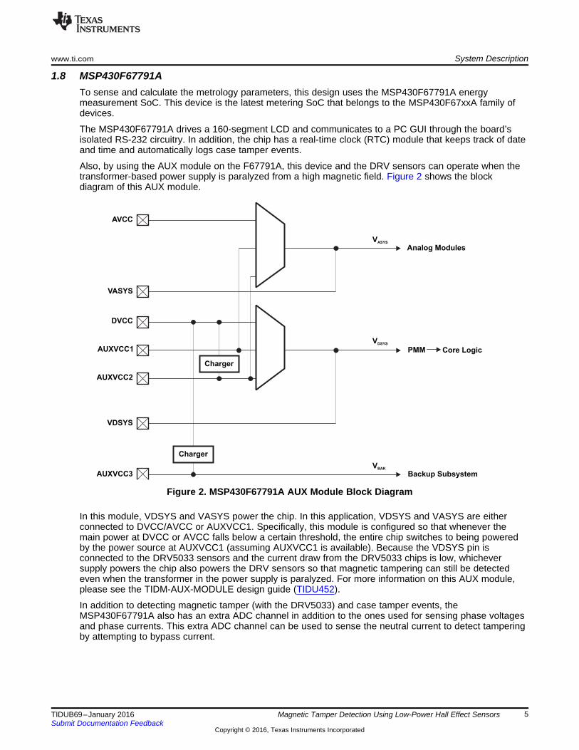
Also, by using the AUX module on the F67791A, this device and the DRV sensors can operate when thetransformer-based power supply is paralyzed from a high magnetic field. Figure 2 shows the blockdiagram of this AUX module.
Figure 2. MSP430F67791A AUX Module Block Diagram
In this module, VDSYS and VASYS power the chip. In this application, VDSYS and VASYS are eitherconnected to DVCC/AVCC or AUXVCC1. Specifically, this module is configured so that whenever themain power at DVCC or AVCC falls below a certain threshold, the entire chip switches to being poweredby the power source at AUXVCC1 (assuming AUXVCC1 is available). Because the VDSYS pin isconnected to the DRV5033 sensors and the current draw from the DRV5033 chips is low, whicheversupply powers the chip also powers the DRV sensors so that magnetic tampering can still be detectedeven when the transformer in the power supply is paralyzed. For more information on this AUX module,please see the TIDM-AUX-MODULE design guide (TIDU452).
In addition to detecting magnetic tamper (with the DRV5033) and case tamper events, theMSP430F67791A also has an extra ADC channel in addition to the ones used for sensing phase voltagesand phase currents. This extra ADC channel can be used to sense the neutral current to detect tamperingby attempting to bypass current.
5TIDUB69–January 2016 Magnetic Tamper Detection Using Low-Power Hall Effect SensorsSubmit Documentation Feedback
Copyright © 2016, Texas Instruments Incorporated
DRV5033DRV5033
UCC28910Transformer-
Based FlybackPower Supply
Capacitive Power Supply
(TPS54060)
Load
Phase A Phase
C
Phase B
Neu
tral
+
-Sx, COMx
MSP430F67791A
TOTAL kWh
UART RX
UART TX-
Source From Utility
CT
Phase APha
se B
Phase C
6' Modulator
6' Modulator
6' Modulator
+
+
-
+
-
+
-
+
-
VCCVSS
6' Modulator
+
-
+
-
6' Modulator
¯û
24
IA
IB
IC
VA
VB
VN
VN
VC
VN
IN
Neu
tral
CT
CT
CT
Active Energy Pulse
Reactive Energy Pulse
ISO7320VCCVSS
ISO7321VSS
VCC
TRS3232
TPS70933
RS-232 Connection
DTR
RTS
RGNDRS-232GND(RGND)
RS-232VCC
ISO-DVCC
ISO-GND
ISO-ACTIVEISO-REACTIVE
6' Modulator
6' Modulator
VCCVSS
VSSVCCJumper
Selection
AUXVCC1
DRV5033
DRV5033DRV5033
DRV5033
Status LEDs
VSS
Output
VCC
VSS
VCC
Output
3
3
RTCCAPx
6
Px.v
Px.w
Px.x
Py.w
Py.x
VDSYS
Pz.wPz.x
Block Diagram www.ti.com
2 Block Diagram
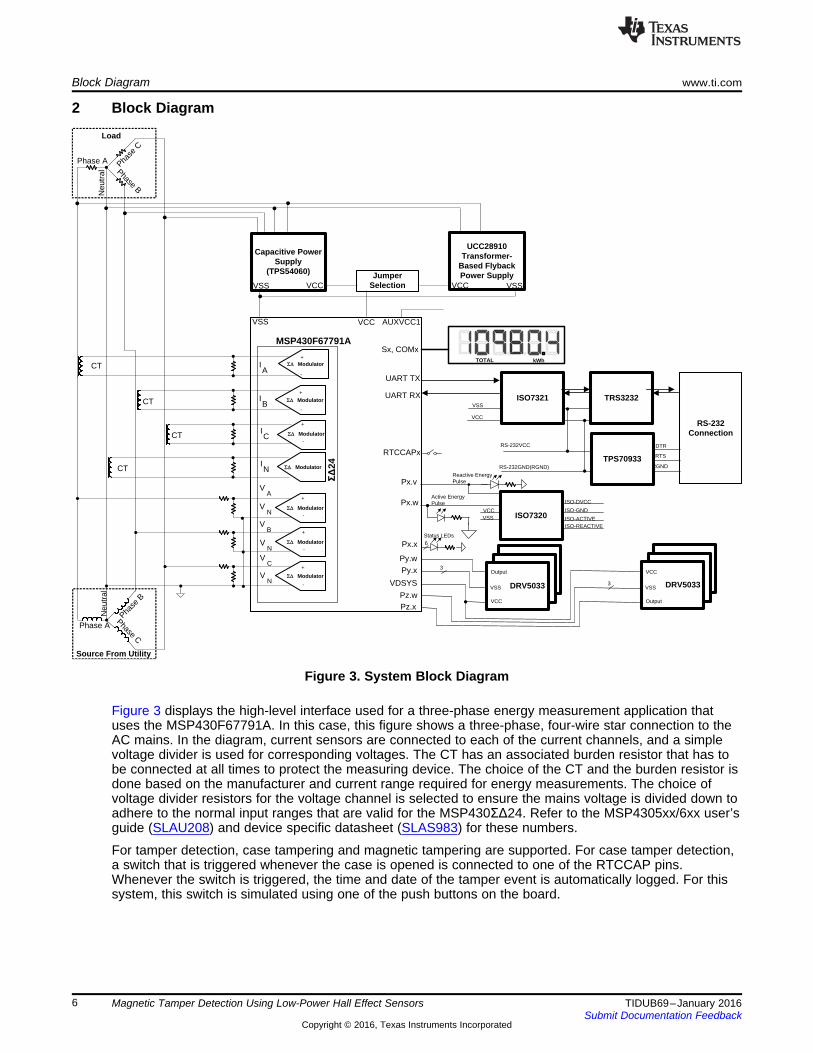
Figure 3. System Block Diagram
Figure 3 displays the high-level interface used for a three-phase energy measurement application thatuses the MSP430F67791A. In this case, this figure shows a three-phase, four-wire star connection to theAC mains. In the diagram, current sensors are connected to each of the current channels, and a simplevoltage divider is used for corresponding voltages. The CT has an associated burden resistor that has tobe connected at all times to protect the measuring device. The choice of the CT and the burden resistor isdone based on the manufacturer and current range required for energy measurements. The choice ofvoltage divider resistors for the voltage channel is selected to ensure the mains voltage is divided down toadhere to the normal input ranges that are valid for the MSP430ΣΔ24. Refer to the MSP4305xx/6xx user’sguide (SLAU208) and device specific datasheet (SLAS983) for these numbers.
For tamper detection, case tampering and magnetic tampering are supported. For case tamper detection,a switch that is triggered whenever the case is opened is connected to one of the RTCCAP pins.Whenever the switch is triggered, the time and date of the tamper event is automatically logged. For thissystem, this switch is simulated using one of the push buttons on the board.
6 Magnetic Tamper Detection Using Low-Power Hall Effect Sensors TIDUB69–January 2016Submit Documentation Feedback
Copyright © 2016, Texas Instruments Incorporated

www.ti.com Block Diagram
In magnetic tamper detection, two sets of three DRV5033 sensors are used. One set of sensors detectsmagnetic tamper events near the current transformers, and the other sensor set senses tamper eventsnear the power supply transformer. All of the sensors have the MSP430F67791A’s VDSYS signal (thesupply used to power the chip) connected to VCC of the sensors. Also, within each set of DRV5033sensors, the outputs of the three sensors are connected to each other (assuming the correct jumpersettings are used). In contrast, the GND pin of each sensor is connected by default jumper settings to adifferent pin on the MSP430F67791A so that each DRV sensor can be enabled or disabled individually.
Figure 3 shows two options for the main power source—a cap-drop supply based on the TPS54060 and atransformer based supply using the UCC28910. When the transformer based supply is used and thetransformer in the supply is paralyzed, the application automatically switches to powering the device andHall sensors from the supply connected between AUXVCC1(+) and VSS(–).
Other signals of interest in Figure 3 are the status LEDs and the active/reactive energy pulses used tomeasure accuracy and calibrate the system. The ISO7320 provides an isolated connection for thesepulses for connecting to non-isolated equipment. In addition to isolated pulses, the design supportsisolated RS-232 communication through the use of the TPS70933, ISO7321, and TRS3232. Find moreinformation on the isolated RS-232 portion of the design at http://www.ti.com/tool/TIDA-00163.
2.1 Highlighted Products
2.1.1 DRV5033The DRV5033 is a chopper-stabilized Hall effect sensor that offers a magnetic sensing solution withsuperior sensitivity stability over temperature and integrated protection features.
The DRV5033 responds the same to both polarities of magnetic field direction. When the applied magneticflux density exceeds the BOP threshold, the DRV5033 open drain output goes low. The output stays lowuntil the field decreases to less than BRP, and then the output goes to high impedance. The output currentsink capability is 30 mA. A wide operating voltage range from 2.5 to 38 V with reverse polarity protectionup to –22 V makes the device suitable for a wide range of industrial applications.
Internal protection functions are provided for reverse supply conditions, load dump, and output short circuitor overcurrent. A summary of features of this device is as follows:• Digital omnipolar-switch Hall sensor• Superior temperature stability
– BOP ±10% over temperature• High sensitivity (BOP and BRP)
– ±6.9 / ±3.5 mT (AJ)• Detects north and south magnetic field• Supports a wide voltage range
– 2.5 to 38 V– No external regulator required
• Wide operating temperature range– TA = –40 to 125°C (Q)
• Open drain output (30-mA sink)• Fast 35-μs typical (50-μs maximum) power-on time• Small package and footprint
– Surface mount 3-pin SOT-23 (DBZ)• 2.92 × 2.37 mm
– Through-hole 3-pin SIP (LPG)• 4.00 × 3.15 mm
7TIDUB69–January 2016 Magnetic Tamper Detection Using Low-Power Hall Effect SensorsSubmit Documentation Feedback
Copyright © 2016, Texas Instruments Incorporated

Block Diagram www.ti.com
2.1.2 UCC28910The UCC28910 is a high-voltage flyback switcher that provides output voltage and current regulationwithout the use of an optical coupler. This device incorporate a 700-V power FET and a controller thatprocess operating information from the flyback auxiliary winding and power FET to provide a preciseoutput voltage and current control. The integrated high-voltage current source for startup, which isswitched off during device operation, and the controller current consumption is dynamically adjusted withthe load. Both enable the very low standby power consumption.
Combining switching frequency and peak primary current modulation, the control algorithms in theUCC28910 allow operating efficiencies to meet or exceed applicable standards. Discontinuous conductionmode (DCM) with valley switching reduces switching losses. Built-in protection features help to keepsecondary and primary component stress levels in check across the operating range. The frequency jitterhelps to reduce EMI filter cost. A summary of this device’s feature is as follows:• Constant-voltage (CV) and constant-current (CC) output regulation without optical-coupler• ±5% output voltage regulation accuracy• ±5% output current regulation with AC line and primary inductance tolerance compensation• 700-V start-up and smart power management enables <30-mW standby power• 115-kHz maximum switching frequency design for high-power density• Valley switching and frequency dithering to ease EMI compliance• Thermal shutdown• Low line and output overvoltage protection
2.1.3 TPS54060The TPS54060A is a 60-V, 0.5-A, step-down regulator with an integrated high-side MOSFET. Currentmode control provides simple external compensation and flexible component selection. A low-ripple pulseskip mode reduces the no load, regulated output supply current to 116 μA. Using the enable pin,shutdown supply current is reduced to 1.3 μA when the enable pin is low.
Undervoltage lockout is internally set at 2.5 V, but can be increased using the enable pin. The outputvoltage startup ramp is controlled by the slow start pin that can also be configured for sequencing ortracking. An open-drain power good signal indicates the output is within 94% to 107% of its nominalvoltage.
2.1.4 ISO7321The ISO7321 provides galvanic isolation up to 3 kVRMS for one minute per UL. This digital isolator has twoisolated channels where one is a forward channel and the other is a reverse channel. Each isolationchannel has a logic input and output buffer separated by a silicon dioxide (SiO2) insulation barrier. Thischip supports a signaling rate of 25 Mbps. The chips can operate from 3.3- and 5-V supply and logiclevels. At the rated voltage, the ISO7321 has over a 25-year isolation integrity.
2.1.5 TRS3232The TRS3232 consists of two line drivers, two line receivers, and a dual charge-pump circuit with ±15-kVESD protection pin to pin (serial-port connection pins, including GND). The device meets the requirementsof TIA/EIA-232-F and provides the electrical interface between an asynchronous communication controllerand the serial-port connector. The charge pump and four small external capacitors allow operation from asingle 3- to 5.5-V supply. The devices operate at data signaling rates up to 250 kbps and a maximum of30-V/μs driver output slew rate.
2.1.6 TPS70933The TPS70933 linear regulator is a ultralow, quiescent current device designed for power-sensitiveapplications. A precision band-gap and error amplifier provides 2% accuracy over temperature. Quiescentcurrent of only 1 μA makes these devices ideal solutions for battery-powered, always-on systems thatrequire very little idle-state power dissipation. This device features thermal-shutdown, current-limit, andreverse-current protections for added safety.
8 Magnetic Tamper Detection Using Low-Power Hall Effect Sensors TIDUB69–January 2016Submit Documentation Feedback
Copyright © 2016, Texas Instruments Incorporated

UnifiedClock
System
512KB256KB128KB
Flash
MCLK
ACLK
SMCLK
CPUXV2and
WorkingRegisters(25 MHz)
EEM(S: 8+2)
XIN XOUT
JTAG,SBW
Interface
Port PJ
eUSCI_A0eUSCI_A1eUSCI_A2eUSCI_A3
(UART,IrDA,SPI)
SD24_B
7 Channel6 Channel4 Channel
ADC10_A
10 Bit200 KSPS
LCD_C
8MUXUp to 320Segments
REF
Reference1.5 V, 2.0 V,
2.5 V
DVCC DVSS AVCC AVSS PA
I/O PortsP1, P2
2×8 I/OsInterrupt,Wakeup
PA1×16 I/Os
P1.x P2.xRST/NMI
32KB16KB
RAM
PJ.x
DMA
3 Channel
PMMAuxiliarySupplies
LDOSVM, SVS
BOR
MPY32
SYS
Watchdog
PortMapping
Controller
CRC16
PD
I/O PortsP7, P8
2×8 I/Os
PD1×16 I/Os
I/O PortsP9, P102×8 I/O
PE1×16 I/O
P7.x P8.x
PC
I/O PortsP5, P6
2×8 I/Os
PC1×16 I/Os
P5.x P6.x
PB
I/O PortsP3, P4
2×8 I/Os
PB1×16 I/Os
P3.x P4.x
eUSCI_B0eUSCI_B1
(SPI, I C)2
RTC_CE
(32 kHz)
AUX1 AUX2 AUX3
TA1TA2TA3
Timer_A2 CC
Registers
Ta0
Timer_A3 CC
Registers
COMP_B(ExternalVoltage
Monitoring)
I/O PortsP11
1×6 I/O
PF1×6 I/O
PF
P9.x P10.x
PE
P11.x
www.ti.com Block Diagram
2.1.7 ISO7320The ISO7320 provides galvanic isolation up to 3 kVRMS for 1 minute per UL. This digital isolator has twoisolated forward channels. Each isolation channel has a logic input and output buffer separated by asilicon dioxide (SiO2) insulation barrier. This chip supports a signaling rate of 25 Mbps. The chips canoperate from a 3.3- and 5-V supply and logic levels. At the rated voltage, the ISO7320 has over a 25-yearisolation integrity.
2.1.8 MSP430F67791AFigure 4 shows the features of the MSP430F67791A.
Figure 4. MSP430F67791A Block Diagram
Similar to the MSP430F67791, the MSP430F67791A belongs to the powerful 16-bit MSP430F6xxplatform. This device finds its application in energy measurement and has the necessary architecture tosupport it. The MSP430F67791A has a powerful 25-MHz CPU with MSP430CPUx architecture. Theanalog front-end (AFE) consists of seven independent 24-bit ΣΔ analog-to-digital converters (ADCs)based on a second-order sigma-delta architecture that supports differential inputs. The sigma-delta ADCs(SD24_B) operate independently and are capable of 24-bit results. They can be grouped together forsimultaneous sampling of voltages and currents on the same trigger. In addition, it also has an integratedgain stage to support gains up to 128 for amplification of low-output current sensors. A 32×32-bithardware multiplier on this chip can further accelerate math intensive operations during energycomputation.
The RTC module on this device supports both offset and temperature compensation to ensure accuratetime keeping. Additionally, the RTC module supports automatic logging of an external event or tamperdetection attempt. Other features of this chip include a module for switching between main and backuppower sources.
9TIDUB69–January 2016 Magnetic Tamper Detection Using Low-Power Hall Effect SensorsSubmit Documentation Feedback
Copyright © 2016, Texas Instruments Incorporated

47p
47p
15n
AGND
AGND
330k 330k 330k
2.3
7K
1k
1k
S20
K2
75
EXCML20A
EXCML20A
AGND
C3
C13
C12
R11 R12 R13
R19
R18
R34
R3
L5
L6
LINE3
NEUTRAL
V3+
V3-
P3+1
NEUTRAL
LINE3
V3
System Design Theory www.ti.com
3 System Design Theory
3.1 Design Hardware Implementation
3.1.1 Analog InputsThe MSP430 AFE, which consists of the ΣΔ ADC, is differential and requires that the input voltages at thepins do not exceed ±930 mV (gain = 1). To meet this specification, the current and voltage inputs need tobe divided down. In addition, the ΣΔ24 allows a maximum negative voltage of –1 V. Therefore, AC signalsfrom mains can be directly interfaced without the need for level shifters.
3.1.1.1 Voltage InputsThe voltage from the mains is usually 230 V or 120 V and for optimal accuracy is usually scaled downwithin 930 mV. In the AFE for voltage, there consists a spike protection varistor, EMI filter beads (whichshould help for ESD testing), a voltage divider network, and a RC low-pass filter that acts like an anti-aliasfilter.
Figure 5. AFE for Voltage Inputs
Figure 5 shows the AFE for voltage inputs for a mains voltage of 230 V. The voltage is brought down toapproximately 549 mVRMS, which is 779 mV at its peak, and fed to the positive input. This voltage is withinthe MSP430ΣΔ analog limits by a safety margin greater than 15%. This margin allows accuratemeasurements even during voltage spike conditions. Additionally, note that the anti-alias resistors on thepositive and negative sides are different because the input impedance to the positive terminal is muchhigher; therefore, a lower value resistor is used for the anti-alias filter. If this is not maintained, a relativelylarge phase shift would result.
10 Magnetic Tamper Detection Using Low-Power Hall Effect Sensors TIDUB69–January 2016Submit Documentation Feedback
Copyright © 2016, Texas Instruments Incorporated

0
47p
47p
15n
AGND
AGND0
AVCC
13
1k
1k
SM
AJ5
.0C
A
AGNDPMLL4148PMLL4148
R/L9C16
C5
C17
R/L10
R2
1
R26
R27
D3
D11
D4
TV
S2
I1+
I1-
D28
D29D30
D31
D32
D12
I1+
I1-
AGND
CUR1+CUR1+
CUR1-CUR1-
I1
www.ti.com System Design Theory
3.1.1.2 Current InputsThe AFE for current inputs is slightly different from the AFE for the voltage inputs. Figure 6 shows the AFEused for a current channel. The AFE for current consists of diodes and transorbs for transient voltagesuppression (TVS). In addition, the front-end consists of EMI filter beads (which help for ESD testing),burden resistors for current transformers, and also an RC low-pass filter that acts like an anti-alias filter.
Figure 6. AFE for Current Inputs
In Figure 6, Resistor R104 is the burden resistor that would be selected based on the current range usedand the turns ratio specification of the CT (CTs with a turns ratio of 2000:1 are used for this design). Thevalue of the burden resistor for this design is around 13 Ω. The antialiasing circuitry, consisting of resistorsand capacitors, follow the burden resistor. Based on this EVM’s maximum current of 100 A, CT turns ratioof 2000:1, and burden resistor of 13 Ω, the input signal to the converter is a fully differential input with avoltage swing of ±919 mV maximum when the maximum current rating of the system (100 A) is applied. Inaddition, footprints for suppressant inductors are also available. These inductor footprints are shown belowas R/L1 and R/L2 and by default are populated with 0-ohm resistors.
3.1.2 Power SupplyThe MSP430 family of microcontrollers support a number of low-power modes in addition to low-powerconsumption during active (measurement) mode when the CPU and other peripherals are active. Becausean energy meter is always interfaced to the AC mains, deriving the DC supply required for the measuringelement (MSP430F67791A) is easy using an AC-to-DC conversion mechanism. The reduced powerrequirements of this device family allow design of power supplies to be small, extremely simple, and cost-effective. The power supply allows the operation of the energy meter by powering it directly from themains.
11TIDUB69–January 2016 Magnetic Tamper Detection Using Low-Power Hall Effect SensorsSubmit Documentation Feedback
Copyright © 2016, Texas Instruments Incorporated

US1J-E3/5AT
10u / 400V
1S
MB
5954B
T3G
US
1M
-13-F
UCC28910D
2.8
7k
0.1u 30.1
k
18u
76.8
k
10
BA
S20H
T1G
CUSTOMTRANS
B130LB-13-F
820u 10u 0.1u
2.0
k
0
D45
C63 D46
D47
U4
IPX4
GND33
GND22
GND11
VS5
VDD6
DRAIN8
R104 C64
R105 C65
R106
R107
D48
T1
1
2
3
4
5
6
7
8 D49
C66 C67 C68
R108
R65
GND
GND
NEUTRAL
NEUTRAL
NEUTRAL
VCC_ISOP3+1
2.2uF10
0u
F/1
00
V
0.22uF/305VAC
0.22uF/305VAC
Vsupply
1N4007
1N4007
1N4757A
1N4757A
0
0.22uF/305VAC1N4007
1N4757A
TPS54060_DGQ_10
1M
33
.2K 1M
0.01uF
0.1
uF
100
100
100
22
.1k
.056uF 100pF
NEUTRAL
NEUTRAL
NEUTRAL
B1
60
1mH
47uF
NEUTRAL
51
.13
1.6
k1
0k
NEUTRAL
C48
C1
02
C46
C50
D20
D22D21
D19
R39
C39D18
D17
U3
BOOT1
VIN2
EN3
SS/TR4
RT/CLK5 PWRGD 6VSENSE 7
COMP 8GND 9
PH 10
R3
5R
37
R3
8
C45
C4
7
R92
R93
R94
R9
5
C60 C61
D2
3
L7
C62
R9
6R
97
R9
8
VCC_PL
DGND
NEUTRAL
P1+1
P2+1
P3+1
+
System Design Theory www.ti.com
3.1.2.1 Cap Drop Power SupplyFigure 7 shows a capacitor power supply that provides a single output voltage of 3.3 V directly from themains of 100- to 240-V ACRMS at 50 or 60 Hz.
Figure 7. Simple Capacitive Power Supply for MSP430 Energy Meter
Appropriate values of resistors (R92, R93, and R94) and capacitors (C39, C46, and C50) are chosenbased on the required output current drive of the power supply. Voltage from mains is directly fed to a RC-based circuit followed by a rectification circuitry to provide a DC voltage for the operation of the MSP430.This DC voltage is regulated to 3.3 V for full speed operation of the MSP430. The design equations for thepower supply are given in the application report Improved Load Current Capability for Cap-Drop Off-LinePower Supply for E-Meter (SLVA491) .This configuration allows all three phases to contribute to thecurrent drive, which is approximately three times the drive available from only one phase. If an evenhigher output drive is required, use the same circuitry followed by an NPN output buffer. Another optionwould be to replace the above circuitry with a transformer- or witching-based power supply.
3.1.2.2 Flyback Power SupplyFigure 8 shows a switching-based power supply that provides a single output voltage of 3.3 V directly fromthe AC mains 100- to 240-VRMS. In Figure 8, the energy measurement system is powered as long as thereis AC voltage on Phase C, corresponding to pad "LINE 3" on the HW and P3+1 on the schematic. A three-phase version of this supply can also be derived as shown in PMP9053.
Figure 8. Flyback Power Supply for MSP430 Energy Meter
12 Magnetic Tamper Detection Using Low-Power Hall Effect Sensors TIDUB69–January 2016Submit Documentation Feedback
Copyright © 2016, Texas Instruments Incorporated

GND
GND
GND
30k
30k
30k
15n
15n
15n
DRVPWR1.
VCC1
GND3
OUT2
VCC1
GND3
OUT2
VCC1
GND3
OUT2
U1G
ND
.U
2G
ND
.U
3G
ND
.
U1O
UT.
U2O
UT.
U3O
UT.
12
DR
V-I
R40
R41
R44
C41
C42
C51
DVSYS_VDSYS
DRV123OUTA
DRV1GND
DRV2GND
DRV3GND
DRVOUT1
DRVOUT2
DRVOUT3
DR
VP
OW
ER
4
1 32
SOT23DRV5033_SOT23
U$1
SOT23DRV5033_SOT23
U$2
SOT23DRV5033_SOT23
U$3
13
21
32
13
2
13
21
32
13
2
www.ti.com System Design Theory
3.1.3 Magnetic Tamper DetectionThe DRV5033 has a BOP of ±6.9 mT and a BRP of ±3.5 mT. For applications where these BOP and BRPsettings are too sensitive for the magnetic flux density that the Hall sensor is actually exposed to, thesensitivity of these devices could be reduced by shielding the sensors.
Figure 9 shows the schematic for one of the two sets of Hall sensors. In the schematic, each DRV5033 ispowered from VDSYS of the MSP430F67791A (assuming the correct jumper settings are used), therebyallowing the DRV5033 sensors to be powered from whichever supply (main or backup) is powering theMSP430F67791A. To measure the current consumption of the set of three Hall sensors, use the DRV-I1jumper.
To reduce the average current consumption of each DRV sensor, the power to the DRV5033 sensor isduty cycled by connecting or disconnecting each sensor’s GND pin. To allow each sensor to be enabledor disabled individually, each sensor’s GND is connected to a different GPIO pin (assuming the correctjumper settings are used) on the MSP430F67791A.
Each Hall effect sensor shown in Figure 9 has an open-drain output that requires a pullup resistor (R45,R47, and R64) . Since all the outputs are open drain, the logical OR of magnetic status can be obtainedby simply connecting the outputs together. In Figure 9, there is an option to connect the outputs of all thesensors in a set to one GPIO pin or connect each DRV sensor to a different GPIO pin by adjusting theposition of the jumper resistors connected to the output. When the outputs of the DRV5033 in a set areconnected, the pullup resistors are effectively in parallel leading to a pullup resistance of 10k. When theyare not connected, the pullup resistances are not in parallel. As a result, the pullup resistors should bechanged from 30k to 10k when the outputs of the DRV sensors are not connected to each other.
Figure 9. Set of Hall Sensors
13TIDUB69–January 2016 Magnetic Tamper Detection Using Low-Power Hall Effect SensorsSubmit Documentation Feedback
Copyright © 2016, Texas Instruments Incorporated

System Design Theory www.ti.com
3.2 Software ImplementationThis section discusses the software for the implementation of three-phase metrology. The first subsectiondiscusses the setup of various peripherals of the MSP430 device. Subsequently, this section describes theentire metrology software as two major processes: the foreground process and background process.
3.2.1 Peripherals SetupThe major peripherals of the MSP430F67791A are the 24-bit sigma delta (SD24_B) ADC, the auxiliarypower supply module (AUX), clock system, RTC, LCD, and watchdog timer (WDT).
3.2.1.1 SD24_B SetupFor a three-phase system, at least six ΣΔs are necessary to independently measure three voltages andcurrents. The code accompanying this design guide addresses the metrology for a three-phase systemwith limited discussion to anti-tampering; however, the code supports the measurement of the neutralcurrent.
The clock to the SD24_B (fM) ADCs derives from the digitally controlled oscillator (DCO) running at 25MHz. The sampling frequency is defined as fS = fM / OSR, the oversampling ratio (OSR) is chosen to be256, and the modulation frequency, fM, is chosen as 1.048576 MHz, resulting in a sampling frequency of4.096 samples per second. The SD24s are configured to generate regular interrupts every samplinginstant.
The following are the ΣΔ channel associations:• A0.0+ and A0.0– → Voltage V1• A1.0+ and A1.0– → Voltage V2• A2.0+ and A2.0– → Voltage V3• A4.0+ and A4.0– → Current I1• A5.0+ and A5.0– → Current I2• A6.0+ and A6.0– → Current I3
Optional neutral channel can be processed through channel A3.0+ and A3.0–.
3.2.1.2 AUX ModuleThe AUX module is set so that hardware switching is enabled for DVCC and AUXVCC1. AUXVCC2 isdisabled. In the software, the SVSMH voltage is set to level 5 because this level is above the 2.5 Vnecessary for the DRV5033 to function properly (see the MSP430F67791A datasheet (SLAS983) for therange of exact voltages that correspond to this particular level) . When VDSYS, the supply selected topower the chip, falls below this SVSMH level, the AUX module triggers for VDSYS to switch to anothersupply (as long as the supply to switch to is above a user-defined threshold). The OK-voltage threshold forAUXVCC1 (AUX1LVL) is level 5. The OK-voltage level for DVCC (AUX0LVL) is level 6. Note that if DVCCwas previously not declared OK, but is later on, the AUX module switches to DVCC even if VDSYS is notbelow the SVSMH level. This auto-switch behavior is only true for DVCC and is not applicable forAUXVCC1 or AUXVCC2.
Whenever the supply powering the chip is switched from DVCC to AUXVCC1 or vice versa, the AUXmodule is configured to generate an interrupt to log this change so that it could later be decided to enter alow-power state with decreased functionality (if switched to AUXVCC1) or exit the low-power state andresume normal functionality (if switched to DVCC).
For more information about the AUX module, see the user’s guide or the following TI design:http://www.ti.com/tool/TIDM-AUX-MODULE.
14 Magnetic Tamper Detection Using Low-Power Hall Effect Sensors TIDUB69–January 2016Submit Documentation Feedback
Copyright © 2016, Texas Instruments Incorporated

www.ti.com System Design Theory
3.2.1.3 Real Time Clock (RTC_C)The RTC_C is a RTC module that is configured to give precise one-second interrupts as well as keeptrack of the time and date. In addition, the RTC_C logs the time of the first tamper event detected onRTCCAP1. This tamper event is simulated by pressing the ABTN3 button on the board. To clear thecurrent tamper event to detect the next tamper event, DBTN2 can be pressed whenever DVCC isavailable.
3.2.1.4 LCD Controller (LCD_C)The LCD controller on the MSP430F67791A can support up to eight-mux displays and 320 segments. TheLCD controller is also equipped with an internal charge pump that can be used for good contrast. In thecurrent design, the LCD controller is configured to work in four-mux mode using 160 segments with arefresh rate set to ACLK/64, which is 512 Hz.
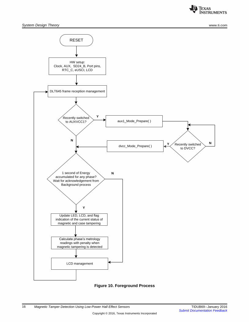
3.2.2 Foreground ProcessThe foreground process includes the initial setup of the MSP430 hardware and software immediately aftera device RESET. Figure 10 shows the flowchart for this process. The initialization routines involve thesetup of the ADC, clock system, auxiliary supply system, general purpose input and output (GPIO) portpins, RTC module for clock functionality, LCD, and the USCI_A0 for universal asynchronous receiver andtransmitter (UART) functionality.
After the hardware is setup, any received frames from the GUI are processed. Once they are processed,the application checks whether the device’s power has just recently been switched to AUXVCC1 due toinsufficient voltage at DVCC. Because AUXVCC1 may be connected to a battery, the current consumptionof the system is reduced by the aux1_Mode_Prepare() function. This aux1_Mode_Prepare() functiondisables the RS-232 circuitry, disables all LEDs, disables the RTC 1-second interrupt (the RTC time-keeping functionality is still enabled though), reduces the active mode clock to approximately 4 MHz,disables the metrology so that there are no sigma-delta interrupts, selects the lowest internal core voltagesetting, and enters LPM3 low-power mode.
15TIDUB69–January 2016 Magnetic Tamper Detection Using Low-Power Hall Effect SensorsSubmit Documentation Feedback
Copyright © 2016, Texas Instruments Incorporated
RESET
HW setup:Clock, AUX, SD24_B, Port pins,
RTC_C, eUSCI, LCD
&DOFXODWH�SKDVH¶V�PHWURORJ\�
readings with penalty when magnetic tampering is detected
1 second of Energy accumulated for any phase?
Wait for acknowledgement from Background process
Y
LCD management
DLT645 frame reception management
N
Recently switched to AUXVCC1? aux1_Mode_Prepare( )
Recently switched to DVCC?
dvcc_Mode_Prepare( )Y N
Y
N
Update LED, LCD, and flag indication of the current status of
magnetic and case tampering
System Design Theory www.ti.com
Figure 10. Foreground Process
16 Magnetic Tamper Detection Using Low-Power Hall Effect Sensors TIDUB69–January 2016Submit Documentation Feedback
Copyright © 2016, Texas Instruments Incorporated

Timer interrupt at 4/sec
Turn ON DRV4, DRV5, and DRV6
Update LCD and set timer_count=0
Return from Interrupt
timer_count=8(2 seconds passed)?
N
Y
N
3URYLGH�§50- to 60-µs delay
Read Hall sensor output
Turn OFF DRV4, DRV5, and DRV6
Read case tampering input pin
timer_count and 3 = 0(1 second passed)?
Update LCD indication of current status of magnetic and case tampering
timer_count++
Y
( )660 10 sI_measurement _DRV5033 Active duty cycle 2700 µA 0.648 µA
0.25 s
-´´ = ´ =
www.ti.com System Design Theory
When in the mode where AUXVCC1 is powering the chip, because the sigma-delta module is disabledand the CPU is only ON in an interrupt service routine, a timer interrupt updates the LCD with newparameters, turning ON the Hall sensors for magnetic tamper detection, and sensing the current state ofthe case tampering input pin. Figure 11 shows the flowchart for the timer interrupt.
As shown in Figure 11, the timer for sensing magnetic and case tampering is set to generate an interruptat a rate of four times per second. For this particular case, only the set of DRV sensors near thetransformer (DRV4, DRV5, and DRV6) are enabled because there is no need to sense near the currenttransformers, which is because metrology calculations would not be calculated while the system ispowered from AUXVCC1. In addition, all sensors are turned ON at the same time to reduce the interruptrate of the timer so that the MSP430F67791A could spend a longer time in LPM3. All of the sensors areturned ON for approximately 50 to 60 μs. With the ON time of 60 μs and a typical 2.7-mA current draw ofthe DRV5033, the current draw from one DRV5033 (with magnetic field not present) can be estimated as:
(1)
Figure 11. Timer Interrupt Flowchart
17TIDUB69–January 2016 Magnetic Tamper Detection Using Low-Power Hall Effect SensorsSubmit Documentation Feedback
Copyright © 2016, Texas Instruments Incorporated
System Design Theory www.ti.com
When the chip switches to being powered to DVCC, the MSP430F67791A exits from the LPM3 low-powermode and enters active mode. After entering active mode, the dvcc_Mode_Prepare() function is called toreverse the changes done by the aux1_Mode_Prepare function. These changes include re-enabling allLEDs, re-enabling the RS-232 circuitry, disabling the timer used for sampling the Hall sensors, increasingthe CPU clock back to 25 MHz, and re-enabling the sigma-delta module to generate interrupts andcalculate metrology parameters.
If the chip is being powered from DVCC, the foreground process checks whether the background processhas notified the foreground process to calculate new metering parameters. This notification isaccomplished through the assertion of the "PHASE_STATUS_NEW_LOG" status flag whenever a frameof data is available for processing. The data frame consists of the processed current, voltage, and activeand reactive quantities that have been accumulated for one second. This accumulation is equivalent to anaccumulation of 50 or 60 cycles of data synchronized to the incoming voltage signal. In addition, a samplecounter keeps tracks of how many samples accumulate over this frame period. This count can vary as thesoftware synchronizes with the incoming mains frequency.
The processed dot products include the VRMS, IRMS, active power, and reactive power. The foregroundprocess uses these dot products to calculate the corresponding metrology readings in real-world units.Processed voltages accumulate in a 48-bit register. In contrast, processed currents, active energies, andreactive energies accumulate in separate 64-bit registers to further process and obtain the RMS and meanvalues. Using the calculated values of active and reactive power from the foreground, the apparent poweris calculated. The frequency (in Hz) and power factor are also calculated using parameters calculated bythe background process using the formulas in Section 3.2.2.1.
Whenever PHASE_STATUS_NEW_LOG is specifically asserted for Phase C, the LEDs LED1 to LED6and LCD are updated to reflect the most recent status of the case and magnetic tamper detection. For theLED and LCD display of tamper detection state, a tamper detection event is declared for a frame of datawhen at least three out of the four previous results within the frame of data indicate a tamper event hasoccurred. After a user-defined consecutive number of frames that have magnetic tampering detected, ametrology penalty can be applied by assuming that the actual current drawn from a consumer’s load isequal to a large, user-defined penalty current instead of the actual measured current. For example, in thisparticular application, the penalty current is set to 100 A, so the RMS current would be set to 100 A andthe active power set equal to (VRMS × 100) W whenever there are a certain number of consecutive framesof magnetic tampering detected.
18 Magnetic Tamper Detection Using Low-Power Hall Effect Sensors TIDUB69–January 2016Submit Documentation Feedback
Copyright © 2016, Texas Instruments Incorporated

2 2APP,ph ACT,ph REACT,phP P P= +
Samplecount
90 ph
n 1REACT,ph REACT,ph
v (n) i (n)
P KSample count
=
´
=
å
Samplecount
ph
n 1ACT,ph ACT,ph
v(n) i (n)
P KSample count
=
´
=
å
Samplecount
ph ph
n 1RMS,ph i,ph offset,ph
i (n) i (n)
I K iSample count
=
´
= ´ -
å
Samplecount
ph ph
n 1RMS,ph v,ph offset,ph
v (n) v (n)
V K vSample count
=
´
= ´ -
å
www.ti.com System Design Theory
3.2.2.1 FormulaeThis section briefly describes the formulas used for the voltage, current, energy, and temperaturecalculations.
As previous sections describe, voltage and current samples are obtained at a sampling rate of 4096 Hz.All of the samples that are taken in one second are kept and used to obtain the RMS values for voltageand current for each phase. The RMS values are obtained by the following formulas:
(2)
(3)
where• ph = Phase parameters that are being calculated [that is, Phase A(= 1), B(= 2), or C(= 3)]• vph(n) = Voltage sample at a sample instant n• voffset,ph = Offset used to subtract effects of the additive white Gaussian noise from the voltage converter• iph(n) = Each current sample at a sample instant n• ioffset,ph = Offset used to subtract effects of the additive white Gaussian noise from the current converter• Sample count = Number of samples in one second• Kv,ph = Scaling factor for voltage• Ki,ph = Scaling factor for each current
Power and energy are calculated for a frame’s worth of active and reactive energy samples. Thesesamples are phase corrected and passed on to the foreground process, which uses the number ofsamples (sample count) to calculate phase active and reactive powers through the following formulas:
(4)
(5)
(6)
where• v90 (n) = Voltage sample at a sample instant ‘n’ shifted by 90°• KACT,ph = Scaling factor for active power• KREACT,ph = Scaling factor for reactive power
Note that for reactive energy, the 90° phase shift approach is used for two reasons:1. This approach accurately measures the reactive power for very small currents.2. This approach conforms to the measurement method specified by IEC and ANSI standards.
The calculated mains frequency calculates the 90°-shifted voltage sample. Because the frequency of themains varies, it is important to first measure the mains frequency accurately to phase shift the voltagesamples accordingly (see Section 3.2.3.1.2 for details).
19TIDUB69–January 2016 Magnetic Tamper Detection Using Low-Power Hall Effect SensorsSubmit Documentation Feedback
Copyright © 2016, Texas Instruments Incorporated
3
APP, Cumulative APP,ph
ph 1
E E
=
= å
3
REACT, Cumulative REACT,ph
ph 1
E E
=
= å
3
ACT, Cumulative ACT,ph
ph 1
E E
=
= å
APP ph APP phE P Sample count= ´
REACT, ph REACT, phE P Sample count= ´
ACT, ph ACT, phE P Sample count= ´
3
APP, Cumulative APP,ph
ph 1
P P
=
= å
3
REACT, Cumulative REACT,ph
ph 1
P P
=
= å
3
ACT, Cumulative ACT,ph
ph 1
P P
=
= å
System Design Theory www.ti.com
To get an exact 90° phase shift, interpolation is used between two samples. For these two samples, avoltage sample slightly more than 90° before the current sample is used, and a voltage sample slightlyless than 90° before the current sample is used. The application's phase shift implementation consists ofan integer part and a fractional part. The integer part is realized by providing an N samples delay. Thefractional part is realized by a one-tap FIR filter. In the software, a lookup table provides the filtercoefficients that are used to create the fractional delays.
In addition to calculating the per-phase active and reactive powers, the cumulative sum of theseparameters are also calculated by Equation 7, Equation 8, and Equation 9:
(7)
(8)
(9)
Using the calculated powers, energies are calculated by the following formulas:
(10)
(11)
(12)
From these equations, the energies are also accumulated to calculate the cumulative energies byEquation 13, Equation 14, and Equation 15:
(13)
(14)
(15)
The calculated energies are then accumulated into buffers that store the total amount of energy consumedsince the system reset. Note that these energies are different from the working variables used toaccumulate energy for outputting energy pulses. There are four sets of buffers that are available: one foreach phase and one for the cumulative of the phases. Within each set of buffers, the following energiesare accumulated:1. Active import energy (active energy when active energy ≥ 0)2. Active export energy (active energy when active energy < 0)3. Reactive Quad I energy (reactive energy when reactive energy ≥ 0 and active power ≥ 0;
inductive load)4. Reactive Quad II energy (reactive energy when reactive energy ≥ 0 and active power < 0;
capacitive generator)5. Reactive Quad III energy (reactive energy when reactive energy < 0 and active power < 0;
inductive generator)6. Reactive Quad IV energy (reactive energy when reactive energy < 0 and active power ≥ 0;
capacitive load)7. App. import energy (apparent energy when active energy ≥ 0)8. App. export energy (apparent energy when active energy < 0)
20 Magnetic Tamper Detection Using Low-Power Hall Effect Sensors TIDUB69–January 2016Submit Documentation Feedback
Copyright © 2016, Texas Instruments Incorporated

ACT
APPARENT
ACT
APPARENT
P, if capacitive load
PInternal representation of power factor
P, if inductive load
P
ìïï
= íï-ïî
Sampling Rate (samples / second)Frequency (Hz)
Frequency (samples / cycle)=
www.ti.com System Design Theory
The background process also calculates the frequency in terms of samples per mains cycle. Theforeground process then converts this samples–per-mains cycle to Hertz by Equation 16:
(16)
After the active power and apparent power have been calculated, the absolute value of the power factor iscalculated. In the system’s internal representation of power factor, a positive power factor corresponds toa capacitive load; a negative power factor corresponds to an inductive load. The sign of the internalrepresentation of power factor is determined by whether the current leads or lags voltage, which isdetermined in the background process. Therefore, the internal representation of power factor is calculatedby Equation 17:
(17)
21TIDUB69–January 2016 Magnetic Tamper Detection Using Low-Power Hall Effect SensorsSubmit Documentation Feedback
Copyright © 2016, Texas Instruments Incorporated

SD24_B Interrupt
New voltage samples?
Retrieve voltage samples
Retrieve any new current samples
per_sample_dsp()
per_sample_energy_pulse_processing()
Retrieve any new current samples
Retrieve any new current samples
Return from Interrupt
NY
System Design Theory www.ti.com
3.2.3 Background ProcessThe background function deals mainly with timing critical events in software. It uses the ΣΔ interrupt as atrigger to collect voltage and current samples. The ΣΔ interrupt is generated when a new voltage orcurrent sample is ready. All voltage channels are delayed so that the voltage samples for all channels areready at the same time. Once the voltage samples are ready and collected, sample processing is done onthe voltage samples and the previous current samples. This sample processing is done by the"per_sample_dsp()" function, which also performs the necessary sensing for magnetic tamper detection.After sample processing, the background process uses the "per_sample_energy_pulse_processing()" forthe calculation and output of energy-proportional pulses. Figure 12 shows the flowchart for this process.
Figure 12. Background Process
22 Magnetic Tamper Detection Using Low-Power Hall Effect Sensors TIDUB69–January 2016Submit Documentation Feedback
Copyright © 2016, Texas Instruments Incorporated
Select new phase
5HPRYH�UHVLGXDO�'&�IRU�SKDVH¶V�YROWDJH�WKHQ�XSGDWH�
SKDVH¶V�9RMS dot product
5HPRYH�UHVLGXDO�'&�IRU�SKDVH¶V�FXUUHQW��WKHQ�XSGDWH�
WKH�SKDVH¶V�GRW�SURGXFW�IRU��,506, active power, and reactive power
Voltage Sag/Swell Detection
Leading-edge zero-crossing on voltage channel?
Update frequency estimation
All three phases done?
1 second of energy calculated for any of the phases?
Swap dot products between foreground and bacground, store magnetic and case tamper status,
set sample_number variable to 0, then notify foreground process.
Y
Y
Y
N
N
Update current status of magnetic and case tampering
N
Return
www.ti.com System Design Theory
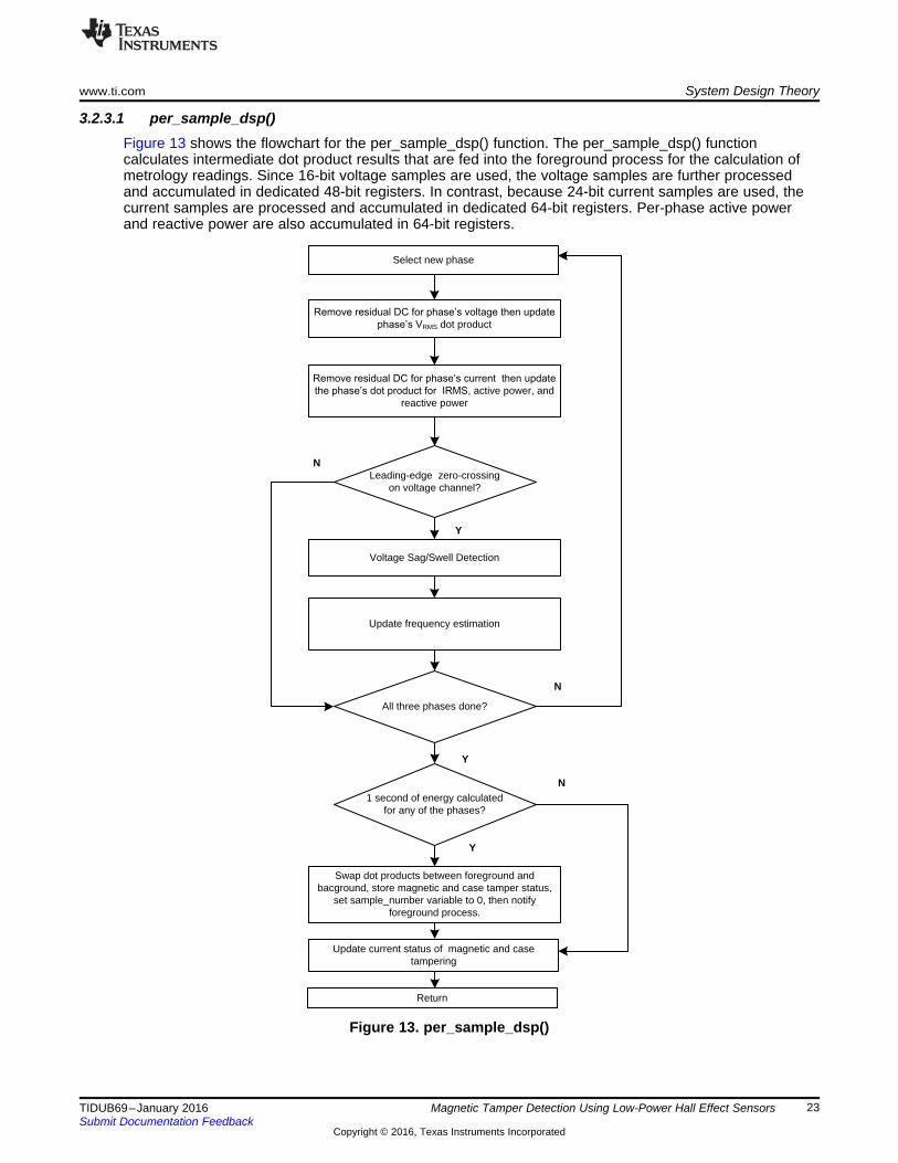
3.2.3.1 per_sample_dsp()Figure 13 shows the flowchart for the per_sample_dsp() function. The per_sample_dsp() functioncalculates intermediate dot product results that are fed into the foreground process for the calculation ofmetrology readings. Since 16-bit voltage samples are used, the voltage samples are further processedand accumulated in dedicated 48-bit registers. In contrast, because 24-bit current samples are used, thecurrent samples are processed and accumulated in dedicated 64-bit registers. Per-phase active powerand reactive power are also accumulated in 64-bit registers.
Figure 13. per_sample_dsp()
23TIDUB69–January 2016 Magnetic Tamper Detection Using Low-Power Hall Effect SensorsSubmit Documentation Feedback
Copyright © 2016, Texas Instruments Incorporated

System Design Theory www.ti.com
Each time the per_sample_dsp() function is called, the application checks if it is time to take a new casetampering or magnetic tampering status reading. The case tamper GPIO pin is read at a rate of 4 Hz.Similarly, each Hall sensor is read at a rate of 4 Hz with the time of sampling of each sensor distributed sothat only one Hall sensor is turned ON at a time.
Also, after sufficient samples (approximately one second's worth) have been accumulated the backgroundprocess triggers the foreground function to calculate the final values of VRMS; IRMS; active, reactive, andapparent powers; active, reactive, and apparent energy; and frequency, and power factor. In the software,there are two sets of dot products: at any given time, one is used by the foreground for calculation and theother used as the working set by the background. After the background process has sufficient samples, itswaps the two dot products so that the foreground uses the newly acquired dot products that thebackground process just calculated, and the background process uses a new empty set to calculate thenext set of dot products. In addition, after the background process has sufficient samples it also stores thepreviously sensed states for magnetic and case tampering so that these states could be used in theforeground process while the background process senses the next states for magnetic and case tamperdetection.
Whenever there is a leading-edge zero-crossing (− to + voltage transition) on a voltage channel, theper_sample_dsp() function is also responsible for updating the corresponding phase’s frequency (insamples per cycle) and voltage sag and swell conditions. For the sag conditions, whenever the RMSvoltage is below a certain user-defined threshold percentage, the number of mains cycles where thiscondition persists is logged as the sag duration. The number of periods in time where there was a sagcondition is logged as the sag events count. Note that the sag duration corresponds to the total number ofcycles in a sag condition since being reset, and is therefore not cleared for every sag event. Also, whenthe RMS voltage is above a certain threshold percentage, swell events and duration are logged in asimilar way.
The following sections describe the various elements of electricity measurement and tamper status updatein the per_sample_dsp() function.
3.2.3.1.1 Voltage and Current SignalsThe output of each SD24_B digital filter is a signed integer and any stray DC or offset value on theseconverters are removed using a DC tracking filter. A separate DC estimate for all voltages and currents isobtained using the filter, voltage, and current samples, respectively. This estimate is then subtracted fromeach voltage and current sample.
The resulting instantaneous voltage and current samples generate the following intermediate results:• Accumulated squared values of voltages and currents, which is used for VRMS and IRMS calculations,
respectively• Accumulated energy samples to calculate active energy• Accumulated energy samples using current and 90° phase-shifted voltage to calculate reactive energy
The foreground process processes these accumulated values.
24 Magnetic Tamper Detection Using Low-Power Hall Effect Sensors TIDUB69–January 2016Submit Documentation Feedback
Copyright © 2016, Texas Instruments Incorporated

www.ti.com System Design Theory
3.2.3.1.2 Frequency Measurement and Cycle TrackingThe instantaneous voltages are accumulated in a 48-bit register. In contrast, the instantaneous currents,active powers, and reactive powers are accumulated in 64-bit registers. A cycle tracking counter andsample counter keep track of the number of samples accumulated. When approximately one second’sworth of samples have been accumulated, the background process stores these accumulation registersand notifies the foreground process to produce the average results, such as RMS and power values.Cycle boundaries trigger the foreground averaging process because this process produces very stableresults.
For frequency measurements, a straight line interpolation is used between the zero crossing voltagesamples. Figure 14 shows the samples near a zero cross and the process of linear interpolation.
Figure 14. Frequency Measurement
Because noise spikes can also cause errors, the application uses a rate of change check to filter out thepossible erroneous signals and make sure that the two points are interpolated from genuine zero crossingpoints. For example, with two negative samples, a noise spike can make one of the samples positive,thereby making the negative and positive pair appear as if there is a zero crossing.
The resultant cycle-to-cycle timing goes through a weak low-pass filter to further smooth out any cycle-to-cycle variations. This filtering results in a stable and accurate frequency measurement that is tolerant ofnoise.
3.2.3.1.3 Magnetic and Case Tampering Status UpdateEach time the per_sample_dsp() function is called, the current status for magnetic and case tamperdetection is updated as is shown in Figure 15. During this process, it is checked whether it is time to readthe case tampering input pin or read any of the Hall sensors. All of the Hall sensors as well as the casetampering input pin are read at a rate of 4 Hz. This 4-Hz rate is achieved by reading each Hall sensor andthe case tampering input pin every 1024(0x3FF) samples. Because the sample rate of the device isapproximately 4096 samples per second, this results in the approximately 4 Hz sample rate for the Hallsensors and case tampering input pin. To distinguish which Hall sensors are sensing magnetic fields, onlyone Hall sensor is turned ON at a time. With there being approximately 1024 samples between the timesa sensor is turned ON and a total of six sensors being sensed, the minimum time between when twodifferent Hall sensors are turned ON is set equal to the floor of (1024/6), which equals 170. The actualDRV sensor that should be turned ON at a new 170 sample interval can be determined by taking the floorof (sample_number/170) then adding 1. For example, at the 850th sample, the (floor(850 / 170)) + 1 = 6th
DRV sensor would be turned ON, which corresponds to U$6 on the board. The case tampering input pinis particularly sampled immediately after DRV1 is turned OFF.
25TIDUB69–January 2016 Magnetic Tamper Detection Using Low-Power Hall Effect SensorsSubmit Documentation Feedback
Copyright © 2016, Texas Instruments Incorporated

Set seq_number variable equal to the logical AND of the sample_number variable and 0x3FF then increment the
sample_number variable
Read Current Status of RTCCAP pin
seq_number Mod 170= 0?
Turn the DRVx hall sensor ON, where x=(floor(sample_number/170)+1)
seq_number Mod 170=1?
Read DRVx hall sensor state then turn it OFF, where x=(floor(sample_number/170)+1)
Y
Y
N
N
seq_number =1?
Return
Y
N
System Design Theory www.ti.com
The sample after a Hall sensor is turned ON, its output is read and then the sensor is turned OFF,resulting in each DRV sensor being turned ON for approximately 244 μs. Although this 244-μs time frameis longer than the minimum 50 μs needed to get a valid output (which means there would be a largercurrent consumption), waiting until the next sample to turn OFF the DRV5033 simplifies the timing of theduty cycling of the power. Also, this 244-μs ON time for the DRV5033 is only applicable when the deviceis running from main power and not when running from the backup power supply. When running frommain power, the current drawn from each DRV sensor that has a 244-μs ON time is still negligiblebecause the system will be running from mains and not a backup battery.
Figure 15. Magnetic and Case Tampering Status Update
3.2.3.2 LED Pulse GenerationIn electricity meters, the energy consumption of the load is normally measured in a fraction of kilowatt-hour (kWh) pulses. This information can be used to accurately calibrate any meter for accuracymeasurement. Typically, the measuring element (the MSP430 microcontroller) is responsible forgenerating pulses proportional to the energy consumed. To serve both these tasks efficiently, the pulsegeneration must be accurate with relatively little jitter. Although time jitters are not an indication of badaccuracy, time jitters give a negative indication of the overall accuracy of the meter. The jitter must beaveraged out due to this negative indication of accuracy.
26 Magnetic Tamper Detection Using Low-Power Hall Effect Sensors TIDUB69–January 2016Submit Documentation Feedback
Copyright © 2016, Texas Instruments Incorporated

SD interrupts at 4096 Hz
Energy accumulator+ = Average power
Energy accumulator = Energy accumulator ±
1 tick
Generate 1 pulse
Proceed to other tasks
Y
N Energy accumulator > 1 tick?
www.ti.com System Design Theory
This application uses average power to generate these energy pulses. The average power (calculated bythe foreground process) accumulates at every ΣΔ interrupt, thereby spreading the accumulated energyfrom the previous one-second timeframe evenly for each interrupt in the current one-second time frame.This accumulation process is equivalent to converting power to energy. When the accumulated energycrosses a threshold, a pulse is generated. The amount of energy above this threshold is kept and a newenergy value is added on top of the threshold in the next interrupt cycle. Because the average powertends to be a stable value, this way of generating energy pulses is very steady and free of jitter.
The threshold determines the energy "tick" specified by meter manufacturers and is a constant. The tick isusually defined in pulses per kWh or just in kWh. One pulse must be generated for every energy tick. Forexample, in this application, the number of pulses generated per kWh is set to 6400 for active and reactiveenergies. The energy tick in this case is 1 kWh/6400. Energy pulses are generated and available on aheader and also through LEDs on the board. GPIO pins are used to produce the pulses.
In the EVM, the LED labeled "Active" corresponds to the active energy consumption for the cumulativethree-phase sum. "Reactive" corresponds to the cumulative three-phase reactive energy sum. The numberof pulses per kWh and each pulse duration can be configured in software. Figure 16 shows the flowdiagram for pulse generation. This flow diagram is valid for pulse generation of active and reactive energy.
Figure 16. Pulse Generation for Energy Indication
The average power is in units of 0.001 W and a 1-kWh threshold is defined as:1-kWh threshold = 1 / 0.001 × 1 KW × (Number of interrupts per sec) × (number of seconds in one hour)aaaaaaaaaaaaaa = 1000000 × 4096 × 3600 = 0xD693A400000 (18)
27TIDUB69–January 2016 Magnetic Tamper Detection Using Low-Power Hall Effect SensorsSubmit Documentation Feedback
Copyright © 2016, Texas Instruments Incorporated

o oIN IN
DegS M
360 f 360 fDelay resolution
OSR f f
´ ´
= =
´
SD24OSRx = 32
Load SD24BPREx
with SD24PREx = 8
System Design Theory www.ti.com
3.2.3.3 Phase CompensationWhen a CT is used as a sensor, it introduces additional phase shift on the current signals. Also, thepassive components of the voltage and current input circuit may introduce another phase shift. The usermust compensate the relative phase shift between voltage and current samples to ensure accuratemeasurements. The ΣΔ converters have programmable delay registers (ΣΔ24PREx) that can be applied toa particular channel. Using this built-in feature (PRELOAD) provides the required phase compensation.Figure 17 shows the usage of PRELOAD to delay sampling on a particular channel.
Figure 17. Phase Compensation Using PRELOAD Register
The fractional delay resolution is a function of input frequency (fIN), OSR, and the sampling frequency (fS).
(19)
In the current application, for an input frequency of 60 Hz, OSR of 256, and sampling frequency of 4096,the resolution for every bit in the preload register is about 0.02° with a maximum of 5.25° (maximum of255 steps). When using CTs that provide a larger phase shift than this maximum, sample delays alongwith fractional delay must be provided.
28 Magnetic Tamper Detection Using Low-Power Hall Effect Sensors TIDUB69–January 2016Submit Documentation Feedback
Copyright © 2016, Texas Instruments Incorporated
IsolatedRS-232
Pulses
LEDs
160-segment LCDButtons
F67791A
AUX
Current front endVoltage front end
Hall sensors
JTAG
FlybackPower supplyHall sensors
Capacitive power supply
www.ti.com Getting Started Hardware
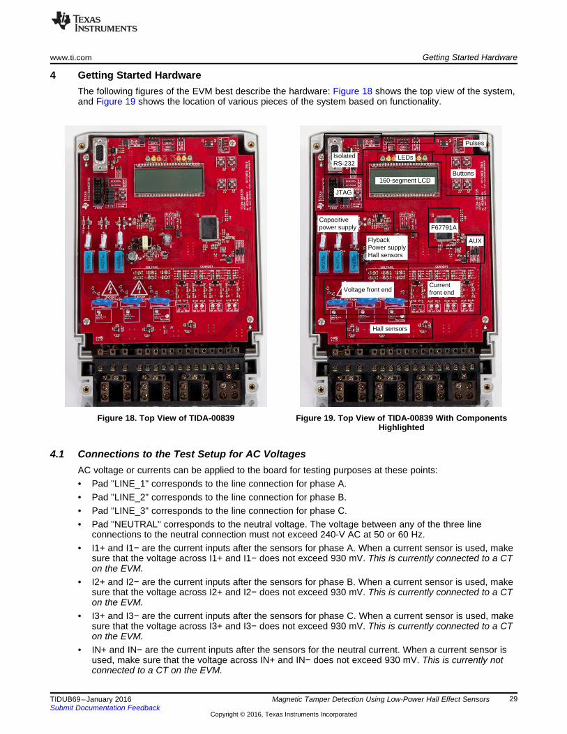
4 Getting Started HardwareThe following figures of the EVM best describe the hardware: Figure 18 shows the top view of the system,and Figure 19 shows the location of various pieces of the system based on functionality.
Figure 18. Top View of TIDA-00839 Figure 19. Top View of TIDA-00839 With ComponentsHighlighted
4.1 Connections to the Test Setup for AC VoltagesAC voltage or currents can be applied to the board for testing purposes at these points:• Pad "LINE_1" corresponds to the line connection for phase A.• Pad "LINE_2" corresponds to the line connection for phase B.• Pad "LINE_3" corresponds to the line connection for phase C.• Pad "NEUTRAL" corresponds to the neutral voltage. The voltage between any of the three line
connections to the neutral connection must not exceed 240-V AC at 50 or 60 Hz.• I1+ and I1− are the current inputs after the sensors for phase A. When a current sensor is used, make
sure that the voltage across I1+ and I1− does not exceed 930 mV. This is currently connected to a CTon the EVM.
• I2+ and I2− are the current inputs after the sensors for phase B. When a current sensor is used, makesure that the voltage across I2+ and I2− does not exceed 930 mV. This is currently connected to a CTon the EVM.
• I3+ and I3− are the current inputs after the sensors for phase C. When a current sensor is used, makesure that the voltage across I3+ and I3− does not exceed 930 mV. This is currently connected to a CTon the EVM.
• IN+ and IN− are the current inputs after the sensors for the neutral current. When a current sensor isused, make sure that the voltage across IN+ and IN− does not exceed 930 mV. This is currently notconnected to a CT on the EVM.
29TIDUB69–January 2016 Magnetic Tamper Detection Using Low-Power Hall Effect SensorsSubmit Documentation Feedback
Copyright © 2016, Texas Instruments Incorporated
IA+ IA± IB+ IB± IC+ IC± VN
VA+ VB+ VC+ VN
Getting Started Hardware www.ti.com
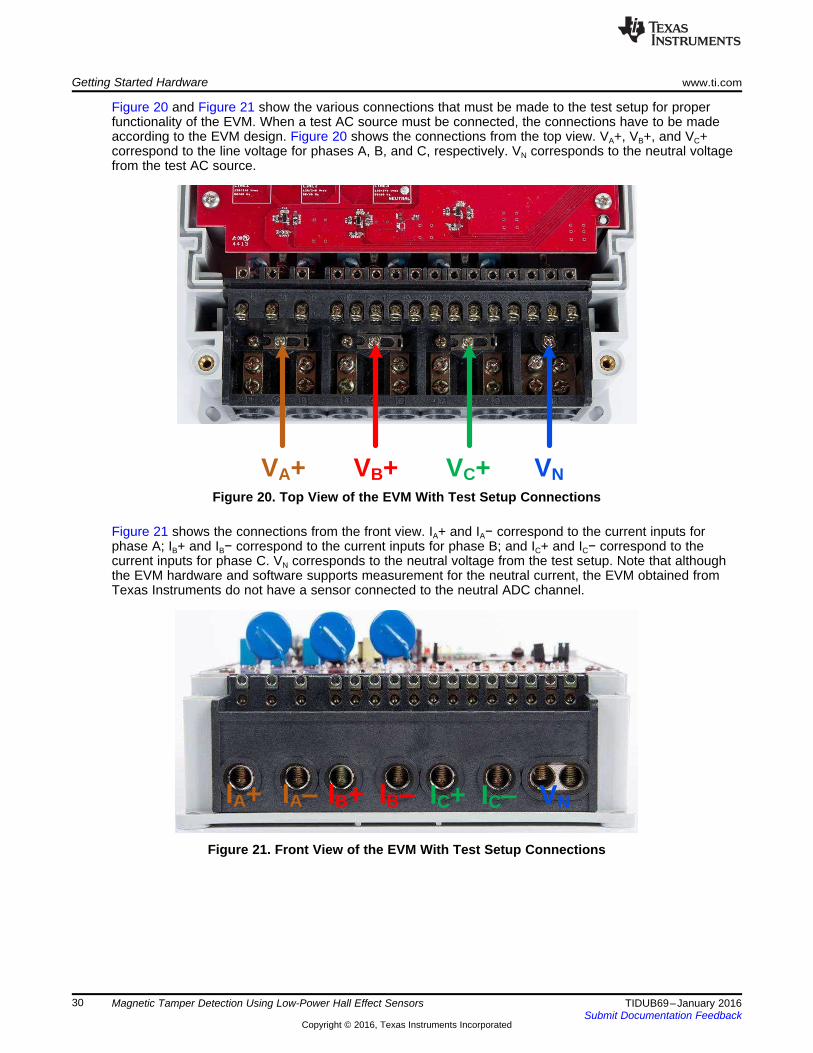
Figure 20 and Figure 21 show the various connections that must be made to the test setup for properfunctionality of the EVM. When a test AC source must be connected, the connections have to be madeaccording to the EVM design. Figure 20 shows the connections from the top view. VA+, VB+, and VC+correspond to the line voltage for phases A, B, and C, respectively. VN corresponds to the neutral voltagefrom the test AC source.
Figure 20. Top View of the EVM With Test Setup Connections
Figure 21 shows the connections from the front view. IA+ and IA− correspond to the current inputs forphase A; IB+ and IB− correspond to the current inputs for phase B; and IC+ and IC− correspond to thecurrent inputs for phase C. VN corresponds to the neutral voltage from the test setup. Note that althoughthe EVM hardware and software supports measurement for the neutral current, the EVM obtained fromTexas Instruments do not have a sensor connected to the neutral ADC channel.
Figure 21. Front View of the EVM With Test Setup Connections
30 Magnetic Tamper Detection Using Low-Power Hall Effect Sensors TIDUB69–January 2016Submit Documentation Feedback
Copyright © 2016, Texas Instruments Incorporated

www.ti.com Getting Started Hardware
4.2 Power Supply Options and Jumper SettingsA single DC voltage rail (DVCC) powers the entire board and the UART communication. DVCC can be derived either through JTAG, externalpower, or the AC mains through either the capacitive power supply or flyback power supplies. Various jumper headers and jumper settings arepresent to add to the flexibility to the board. Some of these headers require that jumpers be placed appropriately for blocks to function correctly.Table 1 shows the functionality of each jumper on the board and the associated functionality.
Table 1. Header Names and Jumper Settings
HEADER ORHEADER OPTION TYPE MAIN FUNCTIONALITY VALID USE CASE COMMENTS
NAMEThis header is not isolated from AC voltage, so do not
ACT (Not isolated, do Active energy pulses Probe between here and ground for connect measuring equipment unless isolators2-pin headernot probe) (WARNING) cumulative three-phase active energy pulses. external to the EVM are available. See theISOLATED ACT header, instead.
Place a jumper here to connect AUXVCC1 to GND. This jumper must be present if AUXVCC1 is notAUXVCC1 selection andAUXVCC1 (Not used as a backup power supply.2-pin header external powerisolated, do not probe) Alternatively, the header can be used to provide a backup power supply to the MSP430. To do so,(WARNING) connect the alternative power supply to this header.Place a jumper here to connect AUXVCC2 to GND. This jumper must be present if AUXVCC2 is not
AUXVCC2 selection; used as a backup power supply.AUXVCC2 (Not 2-pin jumper header AUXVCC2 external power Alternatively, it can be used to provide a backup power supply to the MSP430. To do so, simplyisolated, do not probe) (WARNING) connect the alternative power supply to this header. In this application, AUXVCC2 is not used so ajumper should be placed at this header.
AUXVCC3 (Not AUXVCC3 selection and Place a jumper here to connect AUXVCC3 to VDSYS so that the RTC could be powered byisolated, do not 2-pin jumper header external power whichever supply powers the chip. For this application, placing this jumper is necessary.probe)/JP15 (WARNING)Not a jumper header, probe here for GND Do not probe if board is powered from AC mains,
DGND (Not isolated, Ground voltage header voltage. Connect negative terminal of bench unless the AC mains are isolated. This voltage can beHeaderdo not probe) (WARNING) or external power supply when powering the hot or neutral if AC wall plug is connected to theboard externally. system.This header can be used to disable the set of Do not probe if board is powered from AC mains,Hall sensors near the currentU$1, U$2, U$3 unless the AC mains are isolated. This voltage can betransformers(U$1, U$2, and U$3). To enableEnable/disable and current hot or neutral if AC wall plug is connected to theDRV-I 2-pin jumper header these Hall sensors, place a jumper here. Inconsumption measurement pin system. Please note that whenever the Hall sensorsaddition, this header can be used for taking(WARNING) are disabled by not placing a jumper here thethe average current consumption readings for corresponding Hall sensor LEDs would remain ON.this set of Hall sensors.This header can be used to disable the set of Do not probe if board is powered from AC mains,Hall sensors near the current transformersU$4, U$5, U$6 unless the AC mains are isolated. This voltage can be(U$4, U$5, and U$6). To enable these HallEnable/disable and current hot or neutral if AC wall plug is connected to theDRV-I1 2-pin jumper header sensors, place a jumper here. In addition, thisconsumption measurement pin system. Please note that whenever the Hall sensorsheader can be used for taking the average(WARNING) are disabled by not placing a jumper here thecurrent consumption readings for this set of corresponding Hall sensor LEDs would remain ON.Hall sensors.
31TIDUB69–January 2016 Magnetic Tamper Detection Using Low-Power Hall Effect SensorsSubmit Documentation Feedback
Copyright © 2016, Texas Instruments Incorporated

Getting Started Hardware www.ti.com
Table 1. Header Names and Jumper Settings (continued)HEADER OR
HEADER OPTION TYPE MAIN FUNCTIONALITY VALID USE CASE COMMENTSNAME
Place a 0-Ω resistor between the center padand pad 1 so that U$1, U$2, and U$3 arepowered from AUXVCC1 and DVCC usingexternal diodes to switch between thesupplies. Place a 0-Ω resistor between the3-pad jumper resistor Selection for U$1, U$2, U$3DRVPWR1 center pad and pad 3 to power U$1, U$2, and All three pads should not be shorted together.footprint power source U$3 from AUXVCC1 and DVCC using theinternal switching mechanism of theMSP430F67791A’s AUX module. In thisapplication, the 0-Ω resistor should be placedbetween the center pad and pad 3.Place a 0-Ω resistor between the center padand pad 1 so that U$4, U$5, and U$6 arepowered from AUXVCC1 and DVCC usingexternal diodes to switch between thesupplies. Place a 0-Ω resistor between the3-pad jumper resistor Selection for U$4, U$5, U$6DRVPWR4 center pad and pad 3 to power U$1, U$2, and All three pads should not be shorted together.footprint power source U$3 from AUXVCC1 and DVCC using theinternal switching mechanism of theMSP430F67791A’s AUX module. In thisapplication, the 0-Ω resistor should be placedbetween the center pad and pad 3.Not a jumper header; probe here for VCC
DVCC (Not isolated, VCC voltage header voltage. Connect positive terminal of bench or Do not probe if board is powered from AC mains,Headerdo not probe) (WARNING) external power supply when powering the unless the AC mains are isolated.board externally.
DVCC EXTERNAL (Donot connect JTAG if JTAG external power selection This jumper option and the DVCC INTERNAL jumperPlace a jumper at this header option to selectAC mains is the power Jumper header option option option comprise one three-pin header used to selectexternal voltage for JTAG programming.source ;isolated JTAG (WARNING) the voltage source for JTAG programming.or supply is fine)DVCC INTERNAL (Do Place a jumper at this header option to powerJTAG internal power selection This jumper option and the DVCC EXTERNAL jumpernot connect JTAG if the board using JTAG and to select theJumper header option option option comprise one three-pin header used to selectAC mains is the power voltage from the USB FET for JTAG(WARNING) the voltage source for JTAG programming.source) programming.
Place a jumper only if AC mains voltage is required topower the DVCC rail. This header option and thePlace a jumper at this header position toFlyback power supply select DVCC VCC_PL header option comprise one three-pinDVCC VCC_ISO Jumper header option power the board through AC mains using the(WARNING) header that can be used to select either theflyback power supply. capacitive power supply, flyback power supply, orneither (if jumper not present).
32 Magnetic Tamper Detection Using Low-Power Hall Effect Sensors TIDUB69–January 2016Submit Documentation Feedback
Copyright © 2016, Texas Instruments Incorporated
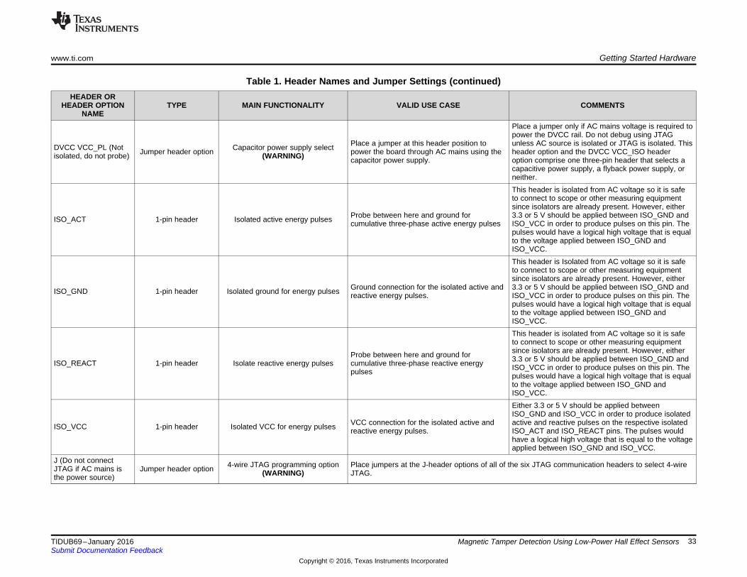
www.ti.com Getting Started Hardware
Table 1. Header Names and Jumper Settings (continued)HEADER OR
HEADER OPTION TYPE MAIN FUNCTIONALITY VALID USE CASE COMMENTSNAME
Place a jumper only if AC mains voltage is required topower the DVCC rail. Do not debug using JTAG
Place a jumper at this header position to unless AC source is isolated or JTAG is isolated. ThisDVCC VCC_PL (Not Capacitor power supply selectJumper header option power the board through AC mains using the header option and the DVCC VCC_ISO headerisolated, do not probe) (WARNING) capacitor power supply. option comprise one three-pin header that selects acapacitive power supply, a flyback power supply, orneither.This header is isolated from AC voltage so it is safeto connect to scope or other measuring equipmentsince isolators are already present. However, either
Probe between here and ground for 3.3 or 5 V should be applied between ISO_GND andISO_ACT 1-pin header Isolated active energy pulses cumulative three-phase active energy pulses ISO_VCC in order to produce pulses on this pin. Thepulses would have a logical high voltage that is equalto the voltage applied between ISO_GND andISO_VCC.This header is Isolated from AC voltage so it is safeto connect to scope or other measuring equipmentsince isolators are already present. However, either
Ground connection for the isolated active and 3.3 or 5 V should be applied between ISO_GND andISO_GND 1-pin header Isolated ground for energy pulses reactive energy pulses. ISO_VCC in order to produce pulses on this pin. Thepulses would have a logical high voltage that is equalto the voltage applied between ISO_GND andISO_VCC.This header is isolated from AC voltage so it is safeto connect to scope or other measuring equipmentsince isolators are already present. However, eitherProbe between here and ground for 3.3 or 5 V should be applied between ISO_GND andISO_REACT 1-pin header Isolate reactive energy pulses cumulative three-phase reactive energy ISO_VCC in order to produce pulses on this pin. Thepulses pulses would have a logical high voltage that is equalto the voltage applied between ISO_GND andISO_VCC.Either 3.3 or 5 V should be applied betweenISO_GND and ISO_VCC in order to produce isolated
VCC connection for the isolated active and active and reactive pulses on the respective isolatedISO_VCC 1-pin header Isolated VCC for energy pulses reactive energy pulses. ISO_ACT and ISO_REACT pins. The pulses wouldhave a logical high voltage that is equal to the voltageapplied between ISO_GND and ISO_VCC.
J (Do not connect 4-wire JTAG programming option Place jumpers at the J-header options of all of the six JTAG communication headers to select 4-wireJTAG if AC mains is Jumper header option (WARNING) JTAG.the power source)
33TIDUB69–January 2016 Magnetic Tamper Detection Using Low-Power Hall Effect SensorsSubmit Documentation Feedback
Copyright © 2016, Texas Instruments Incorporated

Getting Started Hardware www.ti.com
Table 1. Header Names and Jumper Settings (continued)HEADER OR
HEADER OPTION TYPE MAIN FUNCTIONALITY VALID USE CASE COMMENTSNAME
Place jumpers at the six headers to select a JTAGcommunication option. Each of these six headers
Not a jumper header, probe between here have a J option and an S option to select either 4-REACT (Not isolated, Reactive energy pulses1-pin header and ground for cumulative three-phase wire JTAG or SBW. To enable 4-wire JTAG,do not probe) (WARNING) reactive energy pulses. configure all of these headers for the J option. Toenable SBW, configure all of the headers for the Soption.
Ground connection for theRS232_GND 1-pin header Ground connection for the isolated RS-232 circuitry.isolated RS-232Voltage source harvested from Voltage source that is used to power the TRS3232 and ISO7321 for isolated RS-232 communication.RS232_3.3 1-pin header RS-232 line This voltage source is harvested from the RS-232 line.
RTCCLK (Not isolated, RTC calibration2-pin header Probe here to measure the frequency of RTCCLK, which is used for calibrating the RTC.do not probe) (WARNING)RX_EN Jumper header RS-232 receive enable Place a jumper here to enable receiving characters using RS-232.S (Do not connect SBW JTAG programming optionJTAG if AC mains is Jumper header option Place jumpers at the S-header options of all of the six JTAG communication headers to select SBW.(WARNING)the power source)TX_EN Jumper header RS-232 transmit enable Place a jumper here to enable RS-232 transmissions.
Place a 0-Ω resistor between the center padand pad 1 so that U$x’s output is connectedto a GPIO pin that is not shared by other Hallsensors. Place a 0-Ω resistor between theUxOUT (where x is 3-pad jumper resistor Connection selection for the U$x center pad and pad 3 to connect U$x’s output All three pads should not be shorted together.between 1 to 6) footprint Hall sensor’s output pin pin to the GPIO pin that is shared with theother two Hall sensors within that set. In thisapplication, the 0-Ω resistor should be placedbetween the center pad and pad 3.Place a 0-Ω resistor between the center padand pad 1 to connect U$x to ground. Place a0-Ω resistor between the center pad and padUxGND (where x is 3-pad jumper resistor Connection selection for the U$x 3 to connect U$x to a GPIO pin so that the All three pads should not be shorted together.between 1 to 6) footprint Hall sensor’s ground pin power to the device could be duty cycled. Inthis application, the 0-Ω resistor should beplaced between the center pad and pad 3.
34 Magnetic Tamper Detection Using Low-Power Hall Effect Sensors TIDUB69–January 2016Submit Documentation Feedback
Copyright © 2016, Texas Instruments Incorporated

www.ti.com Getting Started Hardware
4.3 LEDS and Buttons
Table 2. Button Functionality
BUTTON NAME DESCRIPTIONABTN3 simulates a case tampering event. The first time this button is pressed is logged and later displayedABTN3 on the LCD. The LCD also displays the current status of whether this button is still pressed or not.
ABT4 Not usedPressing this button clears the first magnetic tampering event so that the next time magnetic tamperingDBTN1 occurs is logged as the "first" magnetic tamper event.Pressing this button clears the first case tampering event so that the next time ABTN3 is pressed this timeDBTN2 is logged as the "first" case tamper event.
Table 3. LED Functionality
LED NAME DESCRIPTIONWhenever the chip is being powered from DVCC, LED1 represents the current state of magnetic sensing
LED1 on U$1. When this LED is ON, magnetic tampering has been detected from the U$1 Hall sensor, which isin the set of Hall sensors near the current transformers.Whenever the chip is being powered from DVCC, LED2 represents the current state of magnetic sensing
LED2 on U$2. When this LED is ON, magnetic tampering has been detected from the U$2 Hall sensor, which isin the set of Hall sensors near the current transformers.Whenever the chip is being powered from DVCC, LED3 represents the current state of magnetic sensing
LED3 on U$3. When this LED is ON, magnetic tampering has been detected from the U$3 Hall sensor, which isin the set of Hall sensors near the current transformers.Whenever the chip is being powered from DVCC, LED4 represents the current state of magnetic sensing
LED4 on U$4. When this LED is ON, magnetic tampering has been detected from the U$4 Hall sensor, which isin the set of Hall sensors near the flyback power supply transformer.Whenever the chip is being powered from DVCC, LED5 represents the current state of magnetic sensing
LED5 on U$5. When this LED is ON, magnetic tampering has been detected from the U$5 Hall sensor, which isin the set of Hall sensors near the flyback power supply transformer.Whenever the chip is being powered from DVCC, LED6 represents the current state of magnetic sensing
LED6 on U$6. When this LED is ON, magnetic tampering has been detected from the U$6 Hall sensor, which isin the set of Hall sensors near the flyback power supply transformer.
LED_ACT This LED corresponds to the cumulative active energy consumption.LED_REACT This LED corresponds to the cumulative reactive energy consumption.
35TIDUB69–January 2016 Magnetic Tamper Detection Using Low-Power Hall Effect SensorsSubmit Documentation Feedback
Copyright © 2016, Texas Instruments Incorporated

Getting Started Firmware www.ti.com
5 Getting Started FirmwareThe source code is developed in the IAR™ environment using the IAR Embedded Workbench® IntegratedDevelopment Environment (IDE) version 6.10.1 for the MSP430 IDE and version 7.0.5.3137 for IARcommon components. Earlier versions of IAR cannot open the project files. When the project is loaded inIAR version 6.x or later, the IDE may prompt the user to create a backup. Click "YES" to proceed. Theenergy metrology software has three main parts:• The toolkit that contains a library of mostly mathematics routines• The metrology code that is used for calculating metrology parameters• The application code that is used for the host-processor functionality of the system (communication,
LCD, RTC setup, and so forth)
Figure 22 shows the contents of the source folder.
Figure 22. Source Folder Structure
Within the emeter-app-6779 folder in the emeter-app folder, the emeter-app-6779.ewp project correspondsto the application code. Similarly, within the emeter-metrology-6779 folder in the emeter-metrology folder,the emeter-metrology-6779.ewp project corresponds to the portion of the code for metrology. Additionally,the folder emeter-toolkit-6779 within the emeter-toolkit has the corresponding toolkit project file emeter-toolkit-6779.ewp. For first-time use, TI recommends to rebuild all three projects by performing the followingsteps:1. Open the IAR IDE.2. Open the F6779 workspace, which is located in the Source folder.3. Within IARs workspace window, click the Overview tab to have a list view of all the projects.4. Right-click the emeter-toolkit-6779 option in the workspace window and select "Rebuild All", as
Figure 22 shows.5. Right-click the emeter-metrology-6779 option in the workspace window and select "Rebuild All", as
Figure 23 shows.6. Within IARs workspace window, click the emeter-app-6779 tab.7. Within the workspace window, select emeter-app-6779, click Rebuild All as Figure 24 shows, and then
download this project onto the MSP430F67791A.
NOTE: If any changes are made to any of the files in the toolkit project and the project is compiled,the metrology project must be recompiled. After recompiling the metrology project, theapplication project must then be recompiled. Similarly, if any changes are made to any of thefiles in the metrology project and the project is compiled, the application project must then berecompiled.
36 Magnetic Tamper Detection Using Low-Power Hall Effect Sensors TIDUB69–January 2016Submit Documentation Feedback
Copyright © 2016, Texas Instruments Incorporated

www.ti.com Getting Started Firmware
Figure 23. Toolkit Project Compilation Figure 24. Metrology Project Compilation Figure 25. Application Project Compilation
37TIDUB69–January 2016 Magnetic Tamper Detection Using Low-Power Hall Effect SensorsSubmit Documentation Feedback
Copyright © 2016, Texas Instruments Incorporated

Regioncount
peak,n n
n 1Avg,bound Region
count
n
n 1
I t
I
t
=
=
´
£
å
å
Test Setup www.ti.com
6 Test Setup
6.1 Metrology Test SetupFor performing metrology testing, a source generator was used to provide the voltages and currents to theboard at the proper locations (see Section 4.1). The design tests used a nominal voltage of 230 V,calibration current of 10 A, and nominal frequency of 50 Hz. In the tests, current is varied from 50 mA to100 A. For each current, a phase shift of 0°, 60°, and −60° is applied between the voltage and current.
When voltage and current are applied to the system, the board outputs active energy pulses at a rate of6400 pulses/kWh. This pulse output feeds into a reference meter that determines the active energy %error (for the equipment used in this test, the reference meter was integrated in the same equipment usedfor the source generator). The active energy % error is based on the actual energy provided to the boardand the measured energy as determined by the active energy output pulse of the system. Based on thisenergy pulse measurement, a plot of active energy % error versus current is created for 0°, 60, and −60°phase shifts, as Section 8.1 shows. A similar method is used to calculate the reactive energy error.
To test the magnetic penalty functionality, 230 V and 10 A are first applied to the system. Subsequently, a1-Tesla magnet is applied close to the system near the CTs. After applying the magnet and observing thecorresponding magnetic tampering LEDs turn ON, the displayed current is verified to be set equal to thepenalty current (100 A by default).
6.2 Current Consumption Test SetupBecause the power to each DRV5033 sensors is duty cycled, using a multimeter to measure the currentconsumption will not provide accurate readings for the average current. As a result, the currentconsumption of a set of DRV sensors is tested by estimating the average of the voltage across a resistorwith known resistance. Specifically, the jumper at DRV-I1 is removed and each end of a resistor isconnected to a different pin of the 2-pin DRV-I1 header. Current consumption readings are taken for thecases where the MSP430F67791A is powered from DVCC and AUXVCC1 because these two cases havedifferent duty cycling schemes and durations. A 49-Ω resistor is connected across DRV-I1 for the caseDVCC is powering the chip and a 10-Ω resistor is used for the case the chip is powered from AUXVCC1.The lower resistance for the AUXVCC1 case is due to the peak current being higher for this case becauseall Hall sensors will be turned ON at the same time compared to the DVCC case where only one sensor isON at a time. In addition, the current consumption is estimated both for when a magnetic tamper event iscurrently being detected and when it is not currently being detected.
Once the resistor is connected to DRV-I1, an oscilloscope is connected to the ends of the resistor. Thewaveform on the oscilloscope is then divided into regions that together cover one period of the waveform.The duration of each region and the associated peak voltage for that region is logged. The peak voltage isconverted to peak current by dividing by the peak voltage by the known resistance value of the resistoracross DRV_I1. Using the different peak currents and durations, an upper-bound of the average current iscalculated by the following formula:
(20)
Since DRV-I1 powers three Hall sensors, this calculated upper bound for average current corresponds tothe current consumption of all three sensors. To calculate the per sensor consumption, the calculatedupper bound for average current is then divided by 3.
38 Magnetic Tamper Detection Using Low-Power Hall Effect Sensors TIDUB69–January 2016Submit Documentation Feedback
Copyright © 2016, Texas Instruments Incorporated

www.ti.com Viewing Metrology Readings and Calibration
7 Viewing Metrology Readings and CalibrationThe values of the metrology parameters can be viewed on the LCD or the GUI.
7.1 Viewing Results Through LCDThe LCD scrolls between parameter values approximately every two seconds. The set of parametersdisplayed on the LCD depends on whether the chip is powered from DVCC or AUXVCC1. For eachparameter that shows on the LCD, three items always display on the screen: a symbol used to denote thephase of the parameter, a text and symbol combination to denote the parameter that is being displayed,and the actual value of the parameter. In addition to the three items always displayed, special characterswill be displayed on the LCD whenever magnetic tampering is currently being detected, the case iscurrently opened, and the device is powered from AUXVCC1. See Figure 26 to Figure 28 for the symbolscorresponding to these statuses.
Figure 26. Symbol for Indicating Figure 27. Symbol for Case Being Figure 28. Symbol for theMagnetic Tampering is Currently Opened MSP430F67791A Being Powered
Detected from AUXVCC1
The phase symbol is displayed at the top of the LCD and denoted by a triangle shape. The orientation ofthe symbol determines the corresponding phase. Figure 29, Figure 30, and Figure 31 show the mappingbetween the different orientations of the triangle and the phase descriptor:
Figure 29. Symbol for Phase A Figure 30. Symbol for Phase B Figure 31. Symbol for Phase C
Aggregate results (such as cumulative active and reactive power) and parameters that are independent ofphase (such as current time and date) are denoted by clearing all of the phase symbols on the LCD.
39TIDUB69–January 2016 Magnetic Tamper Detection Using Low-Power Hall Effect SensorsSubmit Documentation Feedback
Copyright © 2016, Texas Instruments Incorporated

Viewing Metrology Readings and Calibration www.ti.com
The bottom line of the LCD is used to denote the value of the parameter being displayed. The text todenote the parameter being shown displays on the top line of the LCD. Table 4 shows the differentmetering parameters that are displayed on the LCD and the associated units in which they are displayed.The DESIGNATION column shows which characters correspond to which metering parameter.
Table 4. Displayed Parameters
PARAMETER DESIGNATION UNITS COMMENTSThis parameter displays for each phase. Theaggregate active power is also displayed. This isActive power Watts (W) only displayed on the LCD when the chip is beingpowered from DVCC.This parameter displays for each phase. The
Volt-Ampere Reactive aggregate reactive power is also displayed. ThisReactive power (VAR) is only displayed on the LCD when the chip isbeing powered from DVCC.This parameter displays for each phase. This is
Apparent power Volt-Ampere (VA) only displayed on the LCD when the chip is beingpowered from DVCC.This parameter displays for each phase. This isConstant between 0 andPower factor only displayed on the LCD when the chip is being1 powered from DVCC.This parameter displays for each phase. This is
Voltage Volts (V) only displayed on the LCD when the chip is beingpowered from DVCC.This parameter displays for each phase. This is
Current Amps (A) only displayed on the LCD when the chip is beingpowered from DVCC.This parameter displays for each phase. This is
Frequency Hertz (Hz) only displayed on the LCD when the chip is beingpowered from DVCC.This parameter displays for each phase. This isTotal consumed kWh only displayed on the LCD when the chip is beingactive energy powered from DVCC.This parameter displays when the sequence ofaggregate readings are displayed. This displaysTotal consumed kVARH the sum of the reactive energy in quadrant 1 andreactive energy quadrant 4. This is only displayed on the LCDwhen the chip is being powered from DVCC.When the MSP430F67791A is powered fromDVCC, this parameter displays when thesequence of aggregate readings are displayed.This parameter is not displayed once per phase.Current time Hour:minute:second To distinguish between displaying the currenttime, the time of the first magnetic event, and thetime of the first case event, the timer icon isdisplayed on the LCD.When the MSP430F67791A is powered fromDVCC, this parameter displays when thesequence of aggregate readings are displayed.This parameter is not displayed once per phase.Current date Year:month:day To distinguish between displaying the currentdate, the date of the first magnetic event, and thedate of the first case event, the timer icon isdisplayed on the LCD.When the MSP430F67791A is powered fromDVCC, this parameter displays when thesequence of aggregate readings are displayed.This parameter is not displayed once per phase.Time of first To distinguish between displaying the currentmagnetic tamper Hour:minute:second time, the time of the first magnetic event, and theevent time of the first case event, the antennae icon isdisplayed on the LCD. In the case a magnetictamper event has not occurred, the LCD displays"None" for this parameter.
40 Magnetic Tamper Detection Using Low-Power Hall Effect Sensors TIDUB69–January 2016Submit Documentation Feedback
Copyright © 2016, Texas Instruments Incorporated

Pha
se
Des
igna
tion
Value
www.ti.com Viewing Metrology Readings and Calibration
Table 4. Displayed Parameters (continued)PARAMETER DESIGNATION UNITS COMMENTS
When the MSP430F67791A is powered fromDVCC, this parameter displays when thesequence of aggregate readings are displayed.This parameter is not displayed once per phase.Time of first To distinguish between displaying the currentmagnetic tamper Year:month:day date, the date of the first magnetic event, and theevent date of the first case event, the antennae icon isdisplayed on the LCD. In the case a magnetictamper event has not occurred, the LCD displays"None" for this parameter.When the MSP430F67791A is powered fromDVCC, this parameter displays when thesequence of aggregate readings are displayed.This parameter is not displayed once per phase.
Time of first case To distinguish between displaying the currentHour:minute:secondtamper event time, the time of the first magnetic event, and thetime of the first case event, the boxed-R icon isdisplayed on the LCD. In the case a case tamperevent has not occurred, the LCD displays "None"for this parameter.When the MSP430F67791A is powered fromDVCC, this parameter displays when thesequence of aggregate readings are displayed.This parameter is not displayed once per phase.
Time of first case To distinguish between displaying the currentYear:month:daytamper event date, the date of the first magnetic event, and thedate of the first case event, the boxed-R icon isdisplayed on the LCD. In the case a magnetictamper event has not occurred, the LCD displays"None" for this parameter.
Figure 32 shows an example of phase B’s measured power factor of 1 displayed on the LCD when thecase is open and magnetic tampering being currently detected.
Figure 32. LCD
41TIDUB69–January 2016 Magnetic Tamper Detection Using Low-Power Hall Effect SensorsSubmit Documentation Feedback
Copyright © 2016, Texas Instruments Incorporated

Viewing Metrology Readings and Calibration www.ti.com
7.2 Calibrating and Viewing Results Through PC
7.2.1 Viewing ResultsTo view the metrology parameter values from the GUI, perform the following steps:1. Connect the EVM to a PC using an RS-232 cable.2. Open the GUI folder and open calibration-config.xml in a text editor.3. Change the port name field within the meter tag to the COM port connected to the system. As
Figure 33 shows, this field is changed to COM7.
Figure 33. GUI Config File Changed to Communicate With Energy Measurement System
4. Run the calibrator.exe file, which is located in the GUI folder. If the COM port in the calibration-config.xml was changed in the previous step to the COM port connected to the EVM, the GUI opens(see Figure 34). If the GUI connects properly to the EVM, the top-left button is green. If there areproblems with connections or if the code is not configured correctly, the button is red. Click the greenbutton to view the results.
Figure 34. GUI Startup Window
42 Magnetic Tamper Detection Using Low-Power Hall Effect Sensors TIDUB69–January 2016Submit Documentation Feedback
Copyright © 2016, Texas Instruments Incorporated

www.ti.com Viewing Metrology Readings and Calibration
Upon clicking on the green button, the results window opens (see Figure 35). In the figure, there is atrailing "L" or "C" on the Power factor values to indicate an inductive or capacitive load, respectively.
Figure 35. GUI Results Window
From the results window, the total energy consumption readings and sag and swell logs can be viewed byclicking the "Meter consumption" button. After the user clicks this button, the Meter events andconsumption window pops up, as Figure 36 shows.
Figure 36. Meter Events and Consumption Window
From Figure 36, the user can view the meter settings by clicking the "Meter features" button, view thesystem calibration factors by clicking the "Meter calibration factors" button, or open the window used forcalibrating the system by clicking the "Manual cal." button.
43TIDUB69–January 2016 Magnetic Tamper Detection Using Low-Power Hall Effect SensorsSubmit Documentation Feedback
Copyright © 2016, Texas Instruments Incorporated

Viewing Metrology Readings and Calibration www.ti.com
7.2.2 CalibrationCalibration is key to any meter performance and it is absolutely necessary for every meter to go throughthis process. Initially, every meter exhibits different accuracies due to silicon-to-silicon differences, sensoraccuracies, and other passive tolerances. To nullify these effects, every meter must be calibrated. Toperform calibration accurately there should be an accurate AC test source and a reference meteravailable. The source must be able to generate any desired voltage, current, and phase shifts (between Vand I). To calculate errors in measurement, the reference meter acts as an interface between the sourceand the meter being calibrated. This section discusses a simple and effective method of calibration of thisthree-phase EVM.
The GUI used for viewing results can easily be used to calibrate the EVM. During calibration, parameterscalled calibration factors are modified in software to give the least error in measurement. For this meter,there are six main calibration factors for each phase: voltage scaling factor, voltage AC offset, currentscaling factor, current AC offset, power scaling factor, and the phase compensation factor. The voltage,current, and power scaling factors translate measured quantities in metrology software to real-worldvalues represented in volts, amps, and watts, respectively. The voltage AC offset and current AC offseteliminate the effect of additive white Gaussian noise (AWGN) associated with each channel. This noise isorthogonal to everything except itself; as a result, this noise is only present when calculating RMSvoltages and currents. The last calibration factor is the phase compensation factor, which compensatesany phase shifts introduced by the current sensors and other passives. Note that the voltage, current, andpower calibration factors are independent from each other. Therefore, calibrating voltage does not affectthe readings for RMS current or power.
When the meter SW is flashed with the code (available in the *.zip file), default calibration factors areloaded into these calibration factors. These values are to be modified through the GUI during calibration.The calibration factors are stored in INFO_MEM, and therefore, remain the same if the meter is restarted.However, if the code is re-flashed during debugging, the calibration factors are replaced and the meterhas to be recalibrated. One way to save the calibration values is by clicking on the Meter calibrationfactors button (see Figure 35). The Meter calibration factors window (see Figure 37) displays the latestvalues, which can be used to restore calibration values.
Figure 37. Calibration Factors Window
Calibrating any of the scaling factors is referred to as gain correction. Calibrating the phase compensationfactors is referred to as phase correction. For the entire calibration process, the AC test source must beON, meter connections consistent with Section 4.1, and the energy pulses connected to the referencemeter.
44 Magnetic Tamper Detection Using Low-Power Hall Effect Sensors TIDUB69–January 2016Submit Documentation Feedback
Copyright © 2016, Texas Instruments Incorporated

observed
desired
valueCorrection(%) 1 100
value
æ ö= - ´ç ÷
è ø
www.ti.com Viewing Metrology Readings and Calibration
7.2.2.1 Gain CalibrationUsually gain correction for voltage and current can be done simultaneously for all phases. However,energy accuracy (%) from the reference meter for each individual phase is required for gain correction foractive power. Also, when performing active power calibration for any given phase, the other two phasesmust be turned OFF. Typically, switching only the currents OFF is good enough for disabling a phase.
7.2.2.1.1 Voltage and Current Gain CalibrationTo calibrate the voltage and current readings, perform the following steps:1. Connect the GUI to view results for voltage, current, active power, and the other metering parameters.2. Configure the test source to supply desired voltage and current for all phases. Ensure that these are
the voltage and current calibration points with a zero-degree phase shift between each phase voltageand current. For example, for 230 V, 10 A, 0º (PF = 1). Typically, these values are the same for everyphase.
3. Click on the "Manual cal." button that Figure 35 shows. The following screen pops up from Figure 38:
Figure 38. Manual Calibration Window
4. Calculate the correction values for each voltage and current. The correction values that must beentered for the voltage and current fields are calculated by:
(21)where• valueobserved is the value measured by the TI meter• valuedesired is the calibration point configured in the AC test source.
5. After calculating for all voltages and currents, input these values as is (±) for the fields Voltage andCurrent for the corresponding phases.
6. Click on the "Update meter" button and the observed values for the voltages and currents on the GUIsettle to the desired voltages and currents.
45TIDUB69–January 2016 Magnetic Tamper Detection Using Low-Power Hall Effect SensorsSubmit Documentation Feedback
Copyright © 2016, Texas Instruments Incorporated

Viewing Metrology Readings and Calibration www.ti.com
7.2.2.1.2 Active Power Gain Calibration
NOTE: This example is for one phase. Repeat these steps for other phases.
After performing gain correction for voltage and current, gain correction for active power must be done.Gain correction for active power is done differently in comparison to voltage and current. Although,conceptually, calculating using Step 4 with active power readings (displayed on the AC test source) canbe done, this method is not the most accurate and should be avoided.
The best option to get the Correction % is directly from the reference meters measurement error of theactive power. This error is obtained by feeding energy pulses to the reference meter. To perform activepower calibration, perform the following steps:1. Turn off the system and connect the energy pulse output of the system to the reference meter.
Configure the reference meter to measure the active power error based on these pulse inputs.2. Turn on the AC test source.3. Repeat Step 1 to Step 3 from Section 7.2.2.1.1 with the identical voltages, currents, and 0º phase shift
that were used in the same section.4. Obtain the % error in measurement from the reference meter. Note that this value may be negative.5. Enter the error obtained in the previous Step 4 into the Active Power field under the corresponding
phase in the GUI window. This error is already the correction (%) value and does not requirecalculation.
6. Click on Update meter button and the error values on the reference meter immediately settle to a valueclose to zero.
7.2.2.2 Phase CorrectionAfter performing power gain correction, phase calibration must be performed. Similar to active power gaincalibration, to perform phase correction on one phase, the other phases must be disabled. To performphase correction calibration, perform the following steps:1. If the AC test source has been turned OFF or reconfigured, perform Step 1 through Step 3 from
Section 7.2.2.1.1 using the identical voltages and currents used in that section.2. Disable all other phases that are not currently being calibrated by setting the current of these phases to
0 A.3. Modify only the phase-shift to a non-zero value; typically, 60º is chosen. The reference meter now
displays a different % error for active power measurement. Note that this value may be negative.4. If this error from Step 3 is not close to zero, or is unacceptable, perform phase correction by following
these steps:(a) Enter a value as an update for the Phase Correction field for the phase that is being calibrated.
Usually, a small ± integer must be entered to bring the error closer to zero. Additionally, for a phaseshift greater than 0 (for example: 60º), a positive (or negative) error would require a positive(negative) number as correction.
(b) Click on the Update meter button and monitor the error values on the reference meter.(c) If this measurement error (%) is not accurate enough, fine-tune by incrementing or decrementing by
a value of 1 based on Step 4a and Step 4b. Note that after a certain point, the fine-tuning onlyresults in the error oscillating on either side of zero. The value that has the smallest absolute errormust be selected.
(d) Change the phase now to −60° and check if this error is still acceptable. Ideally, errors should besymmetric for same phase shift on lag and lead conditions.
After performing phase correction, calibration is complete for one phase. Note that the gain calibration andphase calibration are completed in sequence for each phase before moving on to other phases. Thesetwo procedures must be repeated for each phase, unlike voltage and current calibration.
46 Magnetic Tamper Detection Using Low-Power Hall Effect Sensors TIDUB69–January 2016Submit Documentation Feedback
Copyright © 2016, Texas Instruments Incorporated

www.ti.com Viewing Metrology Readings and Calibration
This completes calibration of voltage, current, and power for all three phases. View the new calibrationfactors (see Figure 39) by clicking the Meter calibration factors button of the GUI metering results windowin Figure 35.
Figure 39. Calibration Factors Window
Also view the configuration of the system by clicking on the Meter features button in Figure 35 to get tothe window that Figure 40 shows.
Figure 40. Meter Features Window
47TIDUB69–January 2016 Magnetic Tamper Detection Using Low-Power Hall Effect SensorsSubmit Documentation Feedback
Copyright © 2016, Texas Instruments Incorporated
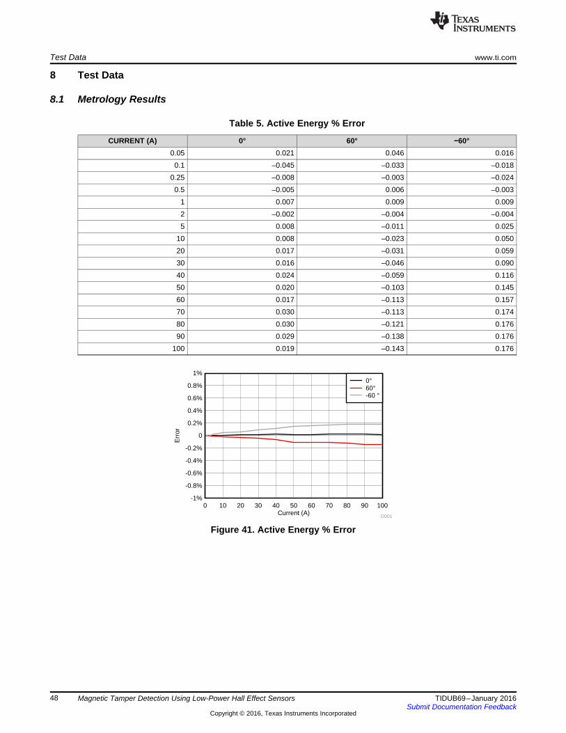
Current (A)
Err
or
0 10 20 30 40 50 60 70 80 90 100-1%
-0.8%
-0.6%
-0.4%
-0.2%
0
0.2%
0.4%
0.6%
0.8%
1%
D001
0°60°-60 °
Test Data www.ti.com
8 Test Data
8.1 Metrology Results
Table 5. Active Energy % Error
CURRENT (A) 0° 60° −60°0.05 0.021 0.046 0.0160.1 –0.045 –0.033 –0.018
0.25 –0.008 –0.003 –0.0240.5 –0.005 0.006 –0.003
1 0.007 0.009 0.0092 –0.002 –0.004 –0.0045 0.008 –0.011 0.025
10 0.008 –0.023 0.05020 0.017 –0.031 0.05930 0.016 –0.046 0.09040 0.024 –0.059 0.11650 0.020 –0.103 0.14560 0.017 –0.113 0.15770 0.030 –0.113 0.17480 0.030 –0.121 0.17690 0.029 –0.138 0.176
100 0.019 –0.143 0.176
Figure 41. Active Energy % Error
48 Magnetic Tamper Detection Using Low-Power Hall Effect Sensors TIDUB69–January 2016Submit Documentation Feedback
Copyright © 2016, Texas Instruments Incorporated
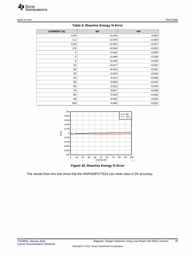
Current (A)
Err
or
0 10 20 30 40 50 60 70 80 90 100-1%
-0.8%
-0.6%
-0.4%
-0.2%
0
0.2%
0.4%
0.6%
0.8%
1%
D002
60°-60 °
www.ti.com Test Data
Table 6. Reactive Energy % Error
CURRENT (A) 60° −60°0.05 –0.070 0.0070.1 –0.075 –0.002
0.25 –0.050 –0.0170.5 –0.034 –0.031
1 –0.032 –0.0262 –0.049 –0.0365 –0.036 –0.036
10 –0.017 –0.03120 –0.024 –0.03130 –0.003 –0.03440 0.012 –0.04650 0.003 –0.04260 0.012 –0.04970 0.027 –0.04880 0.019 –0.06290 0.042 –0.030
100 0.045 –0.032
Figure 42. Reactive Energy % Error
The results from this test show that the MSP430F67791A can meet class 0.2% accuracy.
49TIDUB69–January 2016 Magnetic Tamper Detection Using Low-Power Hall Effect SensorsSubmit Documentation Feedback
Copyright © 2016, Texas Instruments Incorporated

Test Data www.ti.com
8.2 Current Consumption TestingTable 7 through Table 10 show the peak current and duration of different regions for the cases the chip ispowered from DVCC and AUXVCC1 as well as the cases where magnetic tampering is currently detectedand when it is currently not being detected. When running from DVCC, the upper bound for the averagecurrent is less than 20 μA per sensor, which is negligible because DVCC would be powered from mains.In case DVCC is not available and the system is running from AUXVCC1, the upper bound of the currentconsumption per device is reduced to less than 2 μA per sensor.
Table 7. Region Peak Current and Duration, DVCC, Current Magnetic Tampering Not Present
CALCULATED PEAKREGION NUMBER PEAK MEASURED VOLTAGE DURATION CURRENT1 304 mV 36 µs 6204 µA2 136 mV 224 µs 2776 µA3 0 mV 41340 µs 0
Total duration = 36 μs + 224 μs + 41340 μs = 41600 μs
Upper bound for average current of set of Hall sensors = (6204 × 36 + 2776 × 224 + 0 × 41340) / 41600= 20.32 μA
Upper bound for average current of Hall sensor = 20.32 μA / 3 = 6.77 μA
Table 8. Region Peak Current and Duration, DVCC, Current Magnetic Tampering is Present
CALCULATED PEAKREGION NUMBER PEAK MEASURED VOLTAGE DURATION CURRENT1 376 mV 260 µs 7673 µA2 0 mV 41340 µs 0
Total duration = 260 μs + 41340 μs = 41600 μs
Upper bound for average current of set of Hall sensors = (7673 × 260 + 0 × 41340) / 41600 = 47.95 μA
Upper bound for average current of Hall sensor = 47.95 μA / 3 = 15.99 μA
Table 9. Region Peak Current and Duration, AUXVCC1, Current Magnetic Tampering Not Present
CALCULATED PEAKREGION NUMBER PEAK MEASURED VOLTAGE DURATION CURRENT1 148 mV 16 µs 14800 µA2 84 mV 48 µs 8400 µA3 0 mV 249936 µs 0
Total duration = 16 μs + 48 μs + 49936 μs = 250000 μs
Upper bound for average current of set of Hall sensors= (14800 × 16 + 8400 × 48 μs + 0 × 249936 μs) / 250000 μs = 2.56 μA
Upper bound for average current of Hall sensor = 2.56 μA / 3 = 0.853 μA
50 Magnetic Tamper Detection Using Low-Power Hall Effect Sensors TIDUB69–January 2016Submit Documentation Feedback
Copyright © 2016, Texas Instruments Incorporated

www.ti.com Test Data
Table 10. Region Peak Current and Duration, AUXVCC1, Current Magnetic Tampering is Present
CALCULATED PEAKREGION NUMBER PEAK MEASURED VOLTAGE DURATION CURRENT1 208 mV 16 µs 20800 µA2 104 mV 60 µs 10400 µA3 0 mV 249924 µs 0
Total duration = 16 μs + 60 μs + 249924 μs = 250000 μs
Upper bound for average current of set of Hall sensors= (20800 × 16 + 10400 × 60 + 0 × 249924) / 250000 = 3.83 μA
Upper bound for average current of Hall sensor = 20.32 μA / 3 = 1.2757 μA
51TIDUB69–January 2016 Magnetic Tamper Detection Using Low-Power Hall Effect SensorsSubmit Documentation Feedback
Copyright © 2016, Texas Instruments Incorporated

Clock Headers AuxVcc Headers LCD ContrastWatch Crystal
Analog Power Digital Power Status LEDs
User ButtonsLCD
JTAG
23 - JTAG12 - SBWJumper Config
DVCC / DGND Headers
100K
100K
100
47K
12pF
12pF
100
0.1uF
100
100
GND
GND
DVCC
DVCC DVCC
GND
GND
DVCC
GND
DVCC
4.7uF
4.7uF
4.7uF 4.7uF 0.47uF 4.7uF
4.7uF
0.47uF
4.7uF
GND
GND
GND
100nF
AVCC
GND
GND
100nF 100nF 100nF
100nF100nF
GND
10R
100
100
100
100
GND
100K
100K
GND GNDGND
560k
560k
560k
330
100nF 100nF 100nF
DVCC
GND
DVCC
4.7uF
GNDDNP
JTAG
1
3
5
7
9
11
13
2
4
6
12
14
8
10
R53
R50
R56
R51
C40
C37
R55
C53
R54
R57
XT
1
JP
10
1 2 3AU
XV
CC
1124
AU
XV
CC
2123
AUXVCC33
AV
CC
121
AV
SS
1120
AV
SS
211
2
BSL_RX/PM_TA0.1/P2.194
BSL_TX/PM_TA0.0/P2.093
CB3/TA3.1/P11.188
CBOUT/P11.491
COM022
COM123
DV
CC
126
DV
SS
1127
DVSS270
DVSYS69
LCDCAP/R3330
P1.0/TA1.1/VEREF-/A011
P1.1/TA2.1/VEREF+/A110
P1.2/ACLK/A29
P1.3/ADC10CLK/A38
P1.4/MCLK/CB1/A47
P1.5/SMCLK/CB0/A56
P1.6/COM224
P1.7/COM325
P2.4/PM_TA2.012
P2.5/PM_UCB0SOMI/PM_UCB0SCL13
P2.6/PM_UCB0SIMO/PM_UCB0SDA14
P2.7/PM_UCB0CLK15
P3.0/PM_UCA0RXD/PM_UCA0SOMI16
P3.1/PM_UCA0TXD/PM_UCA0SIMO17
P3.2/PM_UCA0CLK18
P3.3/PM_UCA1CLK19
P3.4/PM_UCA1RXD/PM_UCA1SOMI20
P3.5/PM_UCA1TXD/PM_UCA1SIMO21
P3.6/PM_UCA2RXD/PM_UCA2SOMI36
P3.7/PM_UCA2TXD/PM_UCA2SIMO37
P4.0/PM_UCA2CLK38
P4.1
/PM
_U
CA
3R
XD
/M_U
CA
3S
OM
I39
P4.2
/PM
_U
CA
3T
XD
/PM
_U
CA
3S
IMO
40
P4.3
/PM
_U
CA
3C
LK
41
P4
.4/P
M_U
CB
1S
OM
I/P
M_U
CB
1S
CL
42
P4
.5/P
M_U
CB
1S
IMO
/PM
_U
CB
1S
DA
43
P4.6
/PM
_U
CB
1C
LK
44
P4.7
/PM
_TA
3.0
45
P5.0/COM426
P5.1/COM527
P5.2/COM628
P5.3/COM729
P5.4/SDCLK/R2331
P5.5/SD0DIO/LCDREF/R1332
P5.6/SD1DIO/R0333
P5.7/SD2DIO/CB234
P6.0/SD3DIO35
P6.1
/SD
4D
IO/S
39
46
P6.2
/SD
5D
IOS
38
47
P6.3
/SD
6D
IO/S
37
48
P6.4
/S36
49
P6.5
/S35
50
P6.6
/S34
51
P6.7
/S33
52
P7.0
/S32
53
P7.1
/S31
54
P7.2
/S30
55
P7.3
/S29
56
P7.4
/S28
57
P7.5
/S27
58
P7.6
/S26
59
P7.7
/S25
60
P8.0
/S24
61
P8.1
/S23
62
P8.2
/S22
63
P8.3
/S21
64
PM_TA0.2/P2.295
PM_TA1.0/P2.396
RTCCAP05
RTCCAP14
S0/P11.087
S1/P10.786
S2/P10.685
S3/P10.584
S4/P10.483
S5/P10.382
S6/P10.281
S7/P10.180
S8/P10.079
S9/P9.778
S10/P9.677
S11/P9.576
S12/P9.475
S13/P9.374
S14/P9.273
S15/P9.172
S16/P9.071
S17/P8.768
S18/P8.667
S19/P8.566
S20/P8.465
SBWTCK/TEST97
SBWTDIO/NMI/RST102
SD
0P
0103
SD
1N
0106
SD
1P
0105
SD
2N
0108
SD
2P
0107
SD
3N
011
0
SD
3P
0109
SD
4N
011
5
SD
4P
011
4
SD
5N
011
7
SD
5P
011
6
SD
6N
011
9
SD
6P
011
8
SD
PN
0104
TA1.1/P11.289
TA2.1/P11.390
TCK/PJ.3101
TCLK/TDI/PJ.199
TDO/PJ.098
TMS/PJ.2100
TRCCLK/TACLK/P11.592
VA
SY
S1
122
VA
SY
S2
111
VC
OR
E128
VD
SY
S125
VR
EF
113
XIN1
XOUT2
LCD1
1
2
3
4
5
6
7
8
9
10
11
12
13
14
15
16
17
18
19
20
21
22
44
43
42
41
40
39
38
37
36
35
34
33
32
31
30
29
COM0
COM1
COM2
COM3
24
23
C35
C29
C26 C24 C44 C34
C32
C38
C22 C30C31 C28 C23
C36C33
R36
R59
R60
R61
R58
R49
R52
R42
R43
R46
JP41
2
3
JP51
2
3
JP61
2
3
JP71
2
3
JP81
2
3
JP91
2
3
R48
C27 C25 C43
LE
D_A
CT
LE
D3
LE
D2
LE
D1
LE
D_R
EA
CT
LE
D4
LE
D5
LE
D6
DGND
1
2
3
4
DVCC
1
2
3
4
C49
DB
TN
1
12
DB
TN
2
12
AB
TN
3
12
AB
TN
4
12
RE
SE
T
12
RTC
1
2
SV1
12
34
56
TDO
TDO
TDO
TDI
TDI
TMS
TMS
TCK
TCK
TCK
S4
S4
S5
S5
S6
S6
S7
S7
S10
S10
S11
S11
S12
S12
S13
S13
S14
S14
S15
S15
S16
S16
S17
S17
S18
S18
S19
S19
S20
S20
S21
S21
COM0
COM0
COM1
COM1
COM2
COM2
COM3
COM3
S8
S8
S9
S9
R13
R13
R23
R23
R33
R33
S22S
22
S23S
23
S1
S1
VR
EF
VR
EF
S0
S0
S2
S2
S3
S3
AV
CC
GND
GND
DV
CC
DVCC
DV
CC
V1+
V1-
I1+
I1-
I2+
I2-
V2+
V2-
V3+
V3-
I3+
I3-
IN+
IN-
INTEXT
S39
S39
S38
S38
S37
S37
S36
S36
S35
S35
S34
S34
S33
S33
S32
S32
S31
S31
S30
S30
S29
S29
S28
S28
S27
S27
S26
S26
S25
S25
S24
S24
RESET
RESET
BTN1
BTN1
BTN2
BTN2
LE
D1
LED1
LE
D2
LED2
LE
D3
LED3
LE
D4
LE
D4
VA
SY
S1/2
VA
SY
S1/2
VA
SY
S1/2
VA
SY
S1/2
VC
OR
E
VC
OR
E
AU
XV
CC
1
AU
XV
CC
1AUXVCC1
AU
XV
CC
2
AU
XV
CC
2AUXVCC2
AU
XV
CC
3
AUXVCC3
AUXVCC3
AU
XV
CC
3
AU
XV
CC
3
DVSYS_VDSYS
DV
SY
S_V
DS
YS
DV
SY
S_V
DS
YS
DVSYS_VDSYS
RS232_RXDRS232_TXD
AC
T
ACT
RE
AC
T
RE
AC
T
LE
D6
LE
D6
LE
D5
LE
D5
BTN3
BTN3
BTN4
BTN4
XOUT
XOUT
XIN
XIN
DRESET
DRESET
DTCK
DTCK
DTMS
DTMS
DTDI
DTDI
DTDO
DTDO
TEST/SBWTCK
TEST/SBWTCK
TEST/SBWTCK
RTCCLK
RTCCLK
DRV6GNDDRV456OUTADRVOUT6DRVOUT5
DRV5GNDDRV456OUTBDRV4GNDDRVOUT4
DRVOUT1DRV1GNDDRVOUT2
DRV2GND
DRV123OUTBDRV123OUTA
DRVOUT3DRV3GND
MSP430F67791AIPEU
MSP430F67791A
Design Files www.ti.com
9 Design Files
9.1 SchematicsTo download the schematics, see the design files at TIDA-00839.
Figure 43. TIDA-00839 Schematics Page 1
52 Magnetic Tamper Detection Using Low-Power Hall Effect Sensors TIDUB69–January 2016Submit Documentation Feedback
Copyright © 2016, Texas Instruments Incorporated

Analog Front-End (Voltage)Analog Front-End (Current)
0
0
47p
47p
47p
47p
47p
47p
47p
47p
15n
15n
15n
15n
GND
GND
GND
GND
GND
GND
GND
GND
0
0
AVCC
330k 330k 330k
2.3
7K
1k
330k 330k 330k
2.3
7K
1k
1k
12.4
12.4
1k
1k
1k
1k
1k
S20K
275
S20K
275
PMLL4148
PMLL4148
PMLL4148
PMLL4148
PMLL4148
PMLL4148
PMLL4148
EXCML20A
EXCML20AS
MA
J5.0
CA
SM
AJ5.0
CA
0
47p
47p
15n
GND
GND
0
12.4
1k
1k
PMLL4148
PMLL4148
PMLL4148
PMLL4148
SM
AJ5.0
CA 47p
47p
15n
GND
GND
330k 330k 330k
2.3
7K
1k
1k
S20K
275
EXCML20A
EXCML20A
0
47p
47p
15n
GND
GND
GND
0
12.4
1k
1k
PMLL4148
PMLL4148
PMLL4148
PMLL4148
SM
AJ5.0
CA
GND
GND
GND
GND
GND
GND
GND
PMLL4148
PMLL4148
PMLL4148
PMLL4148
PMLL4148
PMLL4148
PMLL4148
PMLL4148
PMLL4148
PMLL4148
PMLL4148
PMLL4148
PMLL4148
PMLL4148
PMLL4148
PMLL4148
PMLL4148
R/L9
R/L11
C2
C11
C16
C5
C18
C6
C1
C9
C8
C10
C17
C19
R/L10
R/L12
R5 R6 R7
R15
R14
R8 R9 R10
R17
R16
R32
R22
R21
R28
R26
R33
R27
R29
R1
R2
D3
D11
D4
D5
D13
D6
D14
L1
L3
TV
S2
TV
S3
R/L13C20
C7
C21
R/L14
R23
R30
R31
D7
D15
D8
D16
TV
S4
C3
C13
C12
R11 R12 R13
R19
R18
R34
R3
L5
L6
R/L7C14
C4
C15
R/L8
R20
R24
R25
D1
D9
D2
D10
TV
S1
LINE1
LINE2
LINE3
NEUTRAL
I1+
I1-
I2+
I2-
I3+
I3-
IN+
IN-
D28
D29D30
D31
D32
D33
D34
D35
D36
D37
D38
D39
D40
D41
D42
D43
D12
V1+P1+1
I2+
I1+
I2-
I1-
V1-
V2+
V2-
P2+1
GND
GND
GND
I3+
I3-
V3+
V3-
P3+1
IN+
IN-
NEUTRAL
NEUTRAL
NEUTRAL
LINE1
LINE2
LINE3
CUR1+CUR1+
CUR1-CUR1-
CUR2+
CUR2-
CUR3+
CUR3-
CURN+
CURN-
V2
I1
I2
V1
I3
V3
IN
www.ti.com Design Files
Figure 44. TIDA-00839 Schematics Page 2
53TIDUB69–January 2016 Magnetic Tamper Detection Using Low-Power Hall Effect SensorsSubmit Documentation Feedback
Copyright © 2016, Texas Instruments Incorporated

DVCC
2.2uF100uF
/100V
0.22uF/305VAC
0.22uF/305VAC
Vsupply
1N4007
1N4007
1N4757A
1N4757A
0
0.22uF/305VAC
1N4007
1N4757A
TPS54060_DGQ_10
1M
33.2
K 1M
0.01uF
0.1
uF
100
100
100
22.1
k
.056uF 100pF
NEUTRAL
NEUTRAL
NEUTRAL
B160
1mH
47uF
NEUTRAL
51.1
31.6
k10k
NEUTRAL
US1J-E3/5AT
10u / 400V
1S
MB
5954B
T3G
US
1M
-13-F
UCC28910D
2.8
7k
0.1u 30.1
k
18u
76.8
k
10
BA
S20H
T1G
CUSTOMTRANS
B130LB-13-F
820u 10u 0.1u
2.0
k
0
C48
C102
C46
C50
D20
D22
D21
D19
R39
C39D18
D17
JP
3
123
U3
BOOT1
VIN2
EN3
SS/TR4
RT/CLK5
PWRGD6
VSENSE7
COMP8
GND9
PH10
R35
R37
R38
C45
C47
R92
R93
R94
R95
C60 C61
D23
L7
C62
R96
R97
R98
D45
C63 D46
D47
U4
IPX4
GND33
GND22
GND11
VS5
VDD6
DRAIN8
R104 C64
R105 C65
R106
R107
D48
T1
1
2
3
4
5
6
7
8 D49
C66 C67 C68
R108
R65
VCC_PL
VCC_PL
GND
GND
GND
NEUTRAL
NEUTRAL
NEUTRAL
NEUTRAL
VCC_ISO
VCC_ISO
P1+1
P2+1
P3+1
P3+1
+
VCC Select
Cap Drop Power Supply
Flyback Power Supply
Design Files www.ti.com
Figure 45. TIDA-00839 Schematics Page 3
54 Magnetic Tamper Detection Using Low-Power Hall Effect Sensors TIDUB69–January 2016Submit Documentation Feedback
Copyright © 2016, Texas Instruments Incorporated

Isolated RS232 Communication
Act / React
GND
GND
TRS3232EQPWRQ1
1N4148
1N414847u
1u
0.1u
0.1u0.1u
0.1u
0.1u0.1u
0.1u
0.1
u
0.1u0.1u
GND
GND
GND
DVCC
DVCC
RX
_E
N
12
TX
_E
N
12
JP11 1
2
JP12 1
2
VCC11
VCC28
INA7
INB3
GND14
GND25
OUTA2
OUTB6
U5
V+2
VCC16
DIN111
DIN210
RIN113
RIN28
C1-3
C1+1
C2-5
C2+4
V-6
GND15
DOUT114
DOUT27
ROUT112
ROUT29
U6
RS1
1
62
73
84
95
G1
G2D50
D51
C69
IN1
EN3
GND2
NC/FB4
OUT5
U7
C70
C71
C72C73
C74
C75
C76
JP141
2
C77
C78
VCC11
INA2
INB3
GND14
GND25
OUTB6
OUTA7
VCC28
U8
1
2
3
4
ISO_PULSE
C79C80
UART_TX
UART_TX
DVCC
GND
GND
ACT
ACT
REACT
REACT
UART_RX
UART_RX
RS232_RXD
RS232_TXD
PORT_RTS
PORT_RTS
PORT_DTRPORT_DTR
+5..12V
VC
C_R
S232
VCC_RS232
VCC_RS232
VCC_RS232
PORT_RX
PORT_RX
PORT_TX
PORT_TX
GND_RS232
GND_RS232
GND_RS232
GND_RS232
GND_RS232
GN
D_R
S232
GND_RS232
ISO7320
ISO7321
TPS70933
www.ti.com Design Files
Figure 46. TIDA-00839 Schematics Page 4
55TIDUB69–January 2016 Magnetic Tamper Detection Using Low-Power Hall Effect SensorsSubmit Documentation Feedback
Copyright © 2016, Texas Instruments Incorporated

0
0
DVCC
GND
GND
GND
GND
GND
GND
GND GND
30k
30k
30k
30k
30k
30k
15n
15n
15n
15n
15n
15n
GND GND
0
0
DVCC
DNP
GND
DN
P
DN
P
4.7uF4.7uF
D24R62
D25R63
DRVPWR1.
VCC1
GND3
OUT2
VCC1
GND3
OUT2
VCC1
GND3
OUT2
VCC1
GND3
OUT2
VCC1
GND2
OUT3
VCC1
GND2
OUT3
U1G
ND
.U
2G
ND
.U
3G
ND
.
U4G
ND
.U
5G
ND
.U
6G
ND
.
U1O
UT.
U2O
UT.
U3O
UT.
U4O
UT.
U5O
UT.
U6O
UT.
12
DR
V-I
1A1
1B2
2Y3
GND4
VCC8
1Y7
2B6
2A5
1A1
1B2
2Y3
GND4
VCC8
1Y7
2B6
2A5
R40
R41
R44
R45
R47
R64
C41
C42
C51
C52
C54
C55
D26R4
D27R66
DRVPWR4.
12
DR
V-I
1
C58
R67
R68
C56C57
AUXVCC1 AUXVCC1
DVCC DVCC
DVSYS_VDSYS DVSYS_VDSYS
DRV123OUTA DRV456OUTA
DRV1GND
DRV2GND
DRV3GND
DRV4GND
DRV5GND
DRV6GND
DRVOUT1
DRVOUT1
DRVOUT2
DRVOUT2
DRVOUT3
DRVOUT3
DRVOUT4
DRVOUT4
DRVOUT5
DRVOUT5
DRVOUT6
DRVOUT6
DRV123OUTB DRV456OUTB
DRVPOWER1
DR
VP
OW
ER
4
1 32
SOT23DRV5033_SOT23
U$1
SOT23DRV5033_SOT23
U$2
SOT23DRV5033_SOT23
U$3
SOT23DRV5033_SOT23
U$4
SIPDRV5033_SIP
U$5
SIPDRV5033_SIP
U$6
13
21
32
13
2
13
21
32
13
2
13
21
32
13
2
13
21
32
13
2
U$7
SN74AUP2G32
U$8
SN74AUP2G32
1 32
Design Files www.ti.com
Figure 47. TIDA-00839 Schematics Page 5
56 Magnetic Tamper Detection Using Low-Power Hall Effect Sensors TIDUB69–January 2016Submit Documentation Feedback
Copyright © 2016, Texas Instruments Incorporated
www.ti.com Design Files
9.2 Bill of MaterialsTo download the bill of materials (BOM), see the design files at TIDA-00839.
9.3 PCB Layout Recommendations• Use ground planes instead of ground traces where possible and minimize the cuts in these ground
planes (especially for critical traces) in the direction of current flow. Ground planes provide a low-impedance ground path which minimizes induced ground noise. However, cuts in the ground plane canincrease inductance. If there are cuts in the ground plane, they should be bridged on the opposite sidewith a 0-Ω resistor.
• When there is a ground plane on both top and bottom layers of a board (such as in our EVM), ensurethere is good stitching between these planes through the liberal use of vias that connect the twoplanes.
• Keep traces short and wide to reduce trace inductance.• Use wide VCC traces and star-routing for these traces instead of point-to-point routing.• Isolate sensitive circuitry from noisy circuitry. For example, high voltage and low voltage circuitry
should be separated.• Use decoupling capacitors with low effective series resistance (ESR) and effective series inductance.
Place decoupling capacitors close to their associated pins.• Minimize the length of the traces used to connect the crystal to the microcontroller. Place guard rings
around the leads of the crystal and ground the crystal housing. In addition, there should be cleanground underneath the crystal and placing any traces underneath the crystal should be prevented.Also, keep high frequency signals away from the crystal.
9.3.1 Layer PlotsTo download the layer plots, see the design files at TIDA-00839.
9.4 CAD ProjectTo download the CAD project files, see the design files at TIDA-00839.
9.5 Gerber FilesTo download the Gerber files, see the design files at TIDA-00839.
10 Software FilesTo download the software files, see the design files at TIDA-00839.
11 References
1. Texas Instruments, Sub-Microamp, Intelligent Hall-Effect Sensing Delivers 20-Year Battery Life, WhitePaper (SLYY058).
12 About the AuthorMEKRE MESGANAW is a Systems Engineer in the Smart Grid and Energy group at Texas Instruments,where he primarily works on grid monitoring customer support and reference design development. Mekrereceived his bachelor of science and master of science in computer engineering from the Georgia Instituteof Technology.
57TIDUB69–January 2016 Magnetic Tamper Detection Using Low-Power Hall Effect SensorsSubmit Documentation Feedback
Copyright © 2016, Texas Instruments Incorporated

IMPORTANT NOTICE FOR TI REFERENCE DESIGNS
Texas Instruments Incorporated ("TI") reference designs are solely intended to assist designers (“Buyers”) who are developing systems thatincorporate TI semiconductor products (also referred to herein as “components”). Buyer understands and agrees that Buyer remainsresponsible for using its independent analysis, evaluation and judgment in designing Buyer’s systems and products.TI reference designs have been created using standard laboratory conditions and engineering practices. TI has not conducted anytesting other than that specifically described in the published documentation for a particular reference design. TI may makecorrections, enhancements, improvements and other changes to its reference designs.Buyers are authorized to use TI reference designs with the TI component(s) identified in each particular reference design and to modify thereference design in the development of their end products. HOWEVER, NO OTHER LICENSE, EXPRESS OR IMPLIED, BY ESTOPPELOR OTHERWISE TO ANY OTHER TI INTELLECTUAL PROPERTY RIGHT, AND NO LICENSE TO ANY THIRD PARTY TECHNOLOGYOR INTELLECTUAL PROPERTY RIGHT, IS GRANTED HEREIN, including but not limited to any patent right, copyright, mask work right,or other intellectual property right relating to any combination, machine, or process in which TI components or services are used.Information published by TI regarding third-party products or services does not constitute a license to use such products or services, or awarranty or endorsement thereof. Use of such information may require a license from a third party under the patents or other intellectualproperty of the third party, or a license from TI under the patents or other intellectual property of TI.TI REFERENCE DESIGNS ARE PROVIDED "AS IS". TI MAKES NO WARRANTIES OR REPRESENTATIONS WITH REGARD TO THEREFERENCE DESIGNS OR USE OF THE REFERENCE DESIGNS, EXPRESS, IMPLIED OR STATUTORY, INCLUDING ACCURACY ORCOMPLETENESS. TI DISCLAIMS ANY WARRANTY OF TITLE AND ANY IMPLIED WARRANTIES OF MERCHANTABILITY, FITNESSFOR A PARTICULAR PURPOSE, QUIET ENJOYMENT, QUIET POSSESSION, AND NON-INFRINGEMENT OF ANY THIRD PARTYINTELLECTUAL PROPERTY RIGHTS WITH REGARD TO TI REFERENCE DESIGNS OR USE THEREOF. TI SHALL NOT BE LIABLEFOR AND SHALL NOT DEFEND OR INDEMNIFY BUYERS AGAINST ANY THIRD PARTY INFRINGEMENT CLAIM THAT RELATES TOOR IS BASED ON A COMBINATION OF COMPONENTS PROVIDED IN A TI REFERENCE DESIGN. IN NO EVENT SHALL TI BELIABLE FOR ANY ACTUAL, SPECIAL, INCIDENTAL, CONSEQUENTIAL OR INDIRECT DAMAGES, HOWEVER CAUSED, ON ANYTHEORY OF LIABILITY AND WHETHER OR NOT TI HAS BEEN ADVISED OF THE POSSIBILITY OF SUCH DAMAGES, ARISING INANY WAY OUT OF TI REFERENCE DESIGNS OR BUYER’S USE OF TI REFERENCE DESIGNS.TI reserves the right to make corrections, enhancements, improvements and other changes to its semiconductor products and services perJESD46, latest issue, and to discontinue any product or service per JESD48, latest issue. Buyers should obtain the latest relevantinformation before placing orders and should verify that such information is current and complete. All semiconductor products are soldsubject to TI’s terms and conditions of sale supplied at the time of order acknowledgment.TI warrants performance of its components to the specifications applicable at the time of sale, in accordance with the warranty in TI’s termsand conditions of sale of semiconductor products. Testing and other quality control techniques for TI components are used to the extent TIdeems necessary to support this warranty. Except where mandated by applicable law, testing of all parameters of each component is notnecessarily performed.TI assumes no liability for applications assistance or the design of Buyers’ products. Buyers are responsible for their products andapplications using TI components. To minimize the risks associated with Buyers’ products and applications, Buyers should provideadequate design and operating safeguards.Reproduction of significant portions of TI information in TI data books, data sheets or reference designs is permissible only if reproduction iswithout alteration and is accompanied by all associated warranties, conditions, limitations, and notices. TI is not responsible or liable forsuch altered documentation. Information of third parties may be subject to additional restrictions.Buyer acknowledges and agrees that it is solely responsible for compliance with all legal, regulatory and safety-related requirementsconcerning its products, and any use of TI components in its applications, notwithstanding any applications-related information or supportthat may be provided by TI. Buyer represents and agrees that it has all the necessary expertise to create and implement safeguards thatanticipate dangerous failures, monitor failures and their consequences, lessen the likelihood of dangerous failures and take appropriateremedial actions. Buyer will fully indemnify TI and its representatives against any damages arising out of the use of any TI components inBuyer’s safety-critical applications.In some cases, TI components may be promoted specifically to facilitate safety-related applications. With such components, TI’s goal is tohelp enable customers to design and create their own end-product solutions that meet applicable functional safety standards andrequirements. Nonetheless, such components are subject to these terms.No TI components are authorized for use in FDA Class III (or similar life-critical medical equipment) unless authorized officers of the partieshave executed an agreement specifically governing such use.Only those TI components that TI has specifically designated as military grade or “enhanced plastic” are designed and intended for use inmilitary/aerospace applications or environments. Buyer acknowledges and agrees that any military or aerospace use of TI components thathave not been so designated is solely at Buyer's risk, and Buyer is solely responsible for compliance with all legal and regulatoryrequirements in connection with such use.TI has specifically designated certain components as meeting ISO/TS16949 requirements, mainly for automotive use. In any case of use ofnon-designated products, TI will not be responsible for any failure to meet ISO/TS16949.IMPORTANT NOTICE
Mailing Address: Texas Instruments, Post Office Box 655303, Dallas, Texas 75265Copyright © 2016, Texas Instruments Incorporated