magneto-ionic control of interfacial...
TRANSCRIPT

LETTERSPUBLISHED ONLINE: 17 NOVEMBER 2014 | DOI: 10.1038/NMAT4134
Magneto-ionic control of interfacial magnetismUwe Bauer1, Lide Yao2, Aik Jun Tan1, Parnika Agrawal1, Satoru Emori1, Harry L. Tuller1,Sebastiaan van Dijken2 and Geo�rey S. D. Beach1*
In metal/oxide heterostructures, rich chemical1,2, electronic3–5,magnetic6–9 and mechanical10,11 properties can emerge frominterfacial chemistry and structure. The possibility to dynam-ically control interface characteristics with an electric fieldpaves the way towards voltage control of these properties insolid-state devices. Here, we show that electrical switchingof the interfacial oxidation state allows for voltage controlof magnetic properties to an extent never before achievedthrough conventional magneto-electric coupling mechanisms.We directly observe in situ voltage-driven O2− migration in aCo/metal-oxide bilayer, which we use to toggle the interfacialmagnetic anisotropy energy by >0.75 erg cm−2 at just 2V.We exploit the thermally activated nature of ion migration tomarkedly increase the switching e�ciency and to demonstratereversible patterning of magnetic properties through localactivation of ionic migration. These results suggest a pathtowards voltage-programmable materials based on solid-stateswitching of interface oxygen chemistry.
The physical and chemical properties of nanoscale materialsderive largely from structure and composition at interfaces. The pos-sibility to electrically modify these interfacial characteristics wouldprovide a powerful means to control material properties. Of par-ticular recent scientific and technological interest are metal/metal-oxide bilayers1–15, inwhich properties as varied as catalytic activity1,2,charge and spin transport3–6, ionic exchange14,15, mechanical be-haviour10,11, thermal conductivity12,13 and magnetism6–9 all dependsensitively on oxygen stoichiometry and defect structure at themetal/metal-oxide interface. Ionic transport in metal oxides can bedriven by an electric field, and O2− migration is already exploitedas a mechanism for resistive switching in anionic metal/oxide/metalmemristors3,4. However, the broader application of voltage-drivenoxygen transport to control interfacial phenomena in metal/metal-oxide structures is only beginning to be explored.
For example, ferromagnetic metal/metal-oxide bilayers such asCo/AlOx and CoFe/MgO exhibit strong perpendicular magneticanisotropy (PMA) derived from interfacial Co–O hybridization8,9.The ability to toggle interfacial PMA with a gate voltage wouldmarkedly reduce switching energies in spintronic devices, andcould enable new device architectures exploiting local gating ofmagnetic properties16–26. Most work on voltage control of magneticanisotropy in metal/metal-oxide bilayers has focused on chargeaccumulation or band shifting in the metal layer16–19. However,experimental reports of irreversibility, and anisotropy changesmuch larger than theoretically predicted20,21, suggest that ioniceffects may be important and in some cases even dominant22–26.Nonetheless, electric-field-driven oxygenmigration inmetal/metal-oxide bilayers is difficult to observe directly, and the impact onmagnetic properties has not yet been established.
Here we report direct in situ observation of voltage-driven O2−
migration in a metal/metal-oxide bilayer, and show that solid-stateelectro-chemical switching of the interfacial oxidation state can beused to completely remove and restore PMA in a thin Co layer.Using cross-sectional transmission electron microscopy (TEM)and high-resolution electron energy-loss spectroscopy (EELS),we track in situ voltage-driven migration of the oxidation frontin a Co/GdOx bilayer. By varying temperature and interfacestructure, we relate motion of the oxidation front to voltage-induced anisotropy changes, and show that by minimizing the O2−
diffusion barrier, the timescale for magneto-ionic switching can bereduced by ∼6 orders of magnitude. We toggle interfacial PMAby an unprecedented >0.75 erg cm−2 at just 2V, and achieve amagneto-electric efficiency>5,000 fJ V−1 m−1. Finally, we introducea general method to reversibly imprint material properties throughlocal activation of ionic migration, which we use to locally patternmagnetic anisotropy and create domain wall (DW) conduits incontinuous magnetic films. These results establish magneto-ioniccoupling as a powerfulmechanism for voltage control ofmagnetism.
Experiments focus on Ta(4 nm)/Pt(3 nm)/Co(0.9 nm)/GdOx(3 nm) films sputter-deposited on thermally oxidized Si (Methods).The films exhibit strong PMA with an in-plane saturation fieldHk ∼ 10 kOe (Supplementary Fig. 3). Square 200 µm × 200 µmGdOx(30 nm)/Ta(2 nm)/Au(12 nm) gate electrodes were patternedon top of the film for voltage application, with the bottom metalstack used as a counter electrode. Figure 1a shows a high-resolutioncross-sectional TEMmicrograph of the layer structure, with the thinCo layer embedded between polycrystalline Pt and GdOx layers.
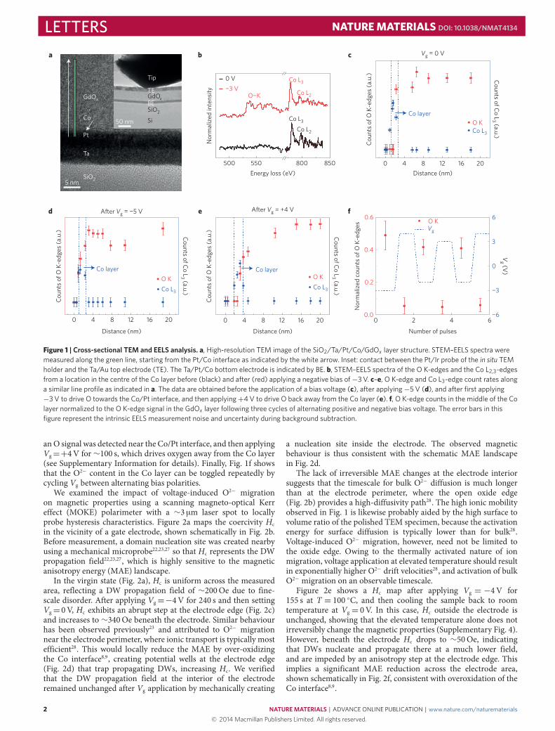
Spatially resolved EELS experiments were carried out in scanningTEM (STEM) mode on the same cross-section to measure thechemical profile and to detect changes induced by a gate voltageVg. Voltage was applied by contacting the top electrode in situwith a Pt/Ir tip as shown in Fig. 1a, inset (see SupplementaryInformation for details). Figure 1b shows representative STEM–EELS spectra with O K-edges and Co white lines from a locationin the centre of the Co layer. The evolution of the O K-edge and CoL3-edge count rates along a line profile perpendicular to the layersis shown in Fig. 1c. The Co layer is clearly distinguished, with noO detected within the Co layer and a sharp rise in the O signal atthe Co/GdOx interface. STEM–EELS scans were then performedafter applying a negative bias, which drives O2− towards the Colayer. The appearance of an O K-edge signal at the centre of theCo layer can be inferred from the spectra in Fig. 1b, taken afterapplying −3V for ∼100 s. After subsequently applying −5V for∼100 s, the STEM–EELS scan in Fig. 1d shows that O penetratesall the way to the bottom Co/Pt interface. Figure 1e,f demonstratesthat Co oxidation is reversible under positive bias. Figure 1e showsa STEM–EELS scan after first applying a negative bias of−3V until
1Department of Materials Science and Engineering, Massachusetts Institute of Technology, Cambridge, Massachusetts 02139, USA. 2NanoSpin,Department of Applied Physics, Aalto University School of Science, PO Box 15100, FI-00076 Aalto, Finland. *e-mail: [email protected]
NATURE MATERIALS | ADVANCE ONLINE PUBLICATION | www.nature.com/naturematerials 1© 2014 Macmillan Publishers Limited. All rights reserved.
LETTERS NATUREMATERIALS DOI: 10.1038/NMAT4134
Tip
TEGdOxGdOxBE
Ta
Pt
Co 50 nm Si
SiO2
SiO25 nm
0 4 8 12 16 20
Distance (nm)
O K
After Vg = −5 V
Coun
ts o
f O K
-edg
es (a
.u.)
Co layer
Co L3
O KCo L3
Counts of Co L3 (a.u.)
0 4 8 12 16 20
O KCo layer
Vg = 0 V
Coun
ts o
f O K
-edg
es (a
.u.)
Distance (nm)
Counts of Co L3 (a.u.)Co L3
0 V−3 V
500 550 800 850
Co L2
Co L2
Co L3
Co L3
Nor
mal
ized
inte
nsity
Energy loss (eV)
O−K
c
d
0 2 4 6−6
−3
0
3
6
Vg
Number of pulses
Vg (V
)
0.0
0.2
0.4
0.6 O K
Nor
mal
ized
cou
nts
of O
K-e
dges
ba
e f
0 4 8 12 16 20
Distance (nm)
After Vg = +4 VCo
unts
of O
K-e
dges
(a.u
.)
Co layer
Counts of Co L3 (a.u.)
Figure 1 | Cross-sectional TEM and EELS analysis. a, High-resolution TEM image of the SiO2/Ta/Pt/Co/GdOx layer structure. STEM–EELS spectra weremeasured along the green line, starting from the Pt/Co interface as indicated by the white arrow. Inset: contact between the Pt/Ir probe of the in situ TEMholder and the Ta/Au top electrode (TE). The Ta/Pt/Co bottom electrode is indicated by BE. b, STEM–EELS spectra of the O K-edges and the Co L2,3-edgesfrom a location in the centre of the Co layer before (black) and after (red) applying a negative bias of−3 V. c–e, O K-edge and Co L3-edge count rates alonga similar line profile as indicated in a. The data are obtained before the application of a bias voltage (c), after applying−5 V (d), and after first applying−3 V to drive O towards the Co/Pt interface, and then applying+4 V to drive O back away from the Co layer (e). f, O K-edge counts in the middle of the Colayer normalized to the O K-edge signal in the GdOx layer following three cycles of alternating positive and negative bias voltage. The error bars in thisfigure represent the intrinsic EELS measurement noise and uncertainty during background subtraction.
anO signal was detected near the Co/Pt interface, and then applyingVg=+4V for ∼100 s, which drives oxygen away from the Co layer(see Supplementary Information for details). Finally, Fig. 1f showsthat the O2− content in the Co layer can be toggled repeatedly bycycling Vg between alternating bias polarities.
We examined the impact of voltage-induced O2− migrationon magnetic properties using a scanning magneto-optical Kerreffect (MOKE) polarimeter with a ∼3 µm laser spot to locallyprobe hysteresis characteristics. Figure 2a maps the coercivity Hcin the vicinity of a gate electrode, shown schematically in Fig. 2b.Before measurement, a domain nucleation site was created nearbyusing a mechanical microprobe22,23,27 so that Hc represents the DWpropagation field22,23,27, which is highly sensitive to the magneticanisotropy energy (MAE) landscape.
In the virgin state (Fig. 2a), Hc is uniform across the measuredarea, reflecting a DW propagation field of ∼200Oe due to fine-scale disorder. After applying Vg=−4V for 240 s and then settingVg=0V, Hc exhibits an abrupt step at the electrode edge (Fig. 2c)and increases to ∼340Oe beneath the electrode. Similar behaviourhas been observed previously23 and attributed to O2− migrationnear the electrode perimeter, where ionic transport is typically mostefficient28. This would locally reduce the MAE by over-oxidizingthe Co interface8,9, creating potential wells at the electrode edge(Fig. 2d) that trap propagating DWs, increasing Hc. We verifiedthat the DW propagation field at the interior of the electroderemained unchanged after Vg application by mechanically creating
a nucleation site inside the electrode. The observed magneticbehaviour is thus consistent with the schematic MAE landscapein Fig. 2d.
The lack of irreversible MAE changes at the electrode interiorsuggests that the timescale for bulk O2− diffusion is much longerthan at the electrode perimeter, where the open oxide edge(Fig. 2b) provides a high-diffusivity path28. The high ionic mobilityobserved in Fig. 1 is likewise probably aided by the high surface tovolume ratio of the polished TEM specimen, because the activationenergy for surface diffusion is typically lower than for bulk28.Voltage-induced O2− migration, however, need not be limited tothe oxide edge. Owing to the thermally activated nature of ionmigration, voltage application at elevated temperature should resultin exponentially higher O2− drift velocities28, and activation of bulkO2− migration on an observable timescale.
Figure 2e shows a Hc map after applying Vg = −4V for155 s at T = 100 ◦C, and then cooling the sample back to roomtemperature at Vg = 0V. In this case, Hc outside the electrode isunchanged, showing that the elevated temperature alone does notirreversibly change the magnetic properties (Supplementary Fig. 4).However, beneath the electrode Hc drops to ∼50Oe, indicatingthat DWs nucleate and propagate there at a much lower field,and are impeded by an anisotropy step at the electrode edge. Thisimplies a significant MAE reduction across the electrode area,shown schematically in Fig. 2f, consistent with overoxidation of theCo interface8,9.
2 NATURE MATERIALS | ADVANCE ONLINE PUBLICATION | www.nature.com/naturematerials© 2014 Macmillan Publishers Limited. All rights reserved.

NATUREMATERIALS DOI: 10.1038/NMAT4134 LETTERS
Au
Vg
GdOx
GdOx
Pt
Ta
Co
SiO2
Ta
Vg < 0, RT
Vg < 0, T > RTM
AE
MA
E
d
f
g h i j k
b
260 260
130
0
130
0
y (µm)x (µm)
−4 V, 155 s, 100 °Ce
260 260
130
0
130
0
y (µm)
x (µm)
−4 V, 240 s, RTc
260 260
130
0
1300
y (µm)x (µm)
Hc
Initial
360
Hc (O
e)
200
40
a
−600 6000 −600 6000 −600 6000
2× 16×
−600 6000Magnetic field (Oe) Magnetic field (Oe) Magnetic field (Oe) Magnetic field (Oe) Magnetic field (Oe)
−600 6000
Kerr
sig
nal (
a.u.
)
Virgin −4 V, 1 s −4 V, 150 s −4 V, 230 s +4 V, 270 s
Figure 2 | Device schematics and voltage control of magnetic anisotropy. a, Topographic map of the coercivity (Hc) in the virgin state, in the vicinity of agate electrode. b, Schematic view of gate-electrode structure. c,d, Hc and the implied MAE landscape, respectively, after applying a gate voltage Vg=−4 Vfor 240 s at room temperature (RT). e,f, The same as in c,d after applying Vg=−4 V for 155 s at 100 ◦C. g–k, Polar MOKE hysteresis loops measured atroom temperature at the centre of the gate electrode showing the device in its virgin state (g), after applying Vg=−4 V at 100 ◦C for 1 s (h), 150 s (i) and230 s (j), and after applying Vg=+4 V at 100 ◦C for 270 s (k). Note that the Kerr signal intensity in i is reduced by a factor of 2 and in j by a factor of 16, asindicated by inset number.
As seen in Fig. 2g–k, the voltage-induced MAE change atT=100 ◦C is progressive. Here, we sequentially applied Vg=−4Vfor a fixed dwell time at T = 100 ◦C, and then cooled the sampleto room temperature with Vg = 0V to measure a hysteresis loopbeneath the electrode. We observe an initial increase in Hc due toDW trap formation at the electrode perimeter, which occurs within1 s of Vg application in contrast to the several minutes requiredat room temperature (Fig. 2c). With increasing voltage dwell timeHc then drops precipitously, indicating a rapid reduction of PMAacross the electrode. The saturation MOKE signal also declines,
by nearly a factor of 2 after ∼150 s (Fig. 2i), suggesting increasingCo oxidation. After several minutes (Fig. 2j), PMA is lost entirely.Remarkably, PMA can be completely restored by reversing thebias polarity, as seen in Fig. 2k after applying Vg=+4V for 270 sat 100 ◦C.
To correlate magnetic anisotropy with the location of theoxidation front, we used a Gd spacer to control the distancebetween Co and the Gd/GdOx interface. Here, GdOx was grown asa continuous 30-nm-thick layer before depositing Ta/Au electrodesto prevent DW trap formation at the edges. Figure 3a–d shows the
NATURE MATERIALS | ADVANCE ONLINE PUBLICATION | www.nature.com/naturematerials 3© 2014 Macmillan Publishers Limited. All rights reserved.

LETTERS NATUREMATERIALS DOI: 10.1038/NMAT4134
PtCo
GdOx
Au
PtCo
GdOx
Au
PtCo
GdOx
Au
PtCo
GdOx
Au
Kerr
sig
nal (
a.u.
)Ke
rr s
igna
l (a.
u.)
Kerr
sig
nal (
a.u.
)
Kerr
sig
nal (
a.u.
)
Kerr
sig
nal (
a.u.
)
Gd
0.3 nm
600 −6000 600
−6 V
−6000 600Magnetic field (Oe)
600
280 s−6 V100 s
+6 V170 s
−6000Magnetic field (Oe)
600 −6000Magnetic field (Oe)
600 −6000Magnetic field (Oe)
600 −6000Magnetic field (Oe)
Magnetic field (Oe) Magnetic field (Oe) Magnetic field (Oe)−6000 600 −6000
Gd
0.7 nmGd
1.0 nm
a
e
b
f
c
g
d
h
Figure 3 | Voltage-induced propagation of oxidation front. a–d, Schematics of Pt/Co/Gd/GdOx samples with di�erent Gd spacer thicknesses (0–1 nm) atthe Co/GdOx interface and polar MOKE hysteresis loops corresponding to the as-deposited samples. e–h, Evolution of polar MOKE hysteresis loops afterapplication of positive (e,f) and negative (h) gate voltage Vg at 100 ◦C to the sample with a 0.7-nm-thick Gd spacer layer (c,g). All hysteresis loops weremeasured at room temperature and zero bias. The red curve in f shows a hysteresis loop after first setting the device in a state with minimum remanenceratio using a negative gate voltage, and then applying a 10 ms voltage pulse Vg=+12 V at 120 ◦C, returning the device close to its initial state.
nominal sample structure and corresponding hysteresis loops forfour samples with increasing Gd spacer thickness d . With a thin Gdspacer, PMA is diminished as evidenced by a significant drop in theremanent magnetization ratioMr/Ms (Fig. 3b), but as d is increasedfurther, PMA again increases (Fig. 3c,d and see SupplementaryFig. 9 and related discussion for more details). We obtainedsimilar results for other metal oxides including Pt/Co/Zr/ZrOxand Pt/Co/Ta/TaOx , and find this behaviour to be rather general.The recovery of PMA for thicker metal overlayers differs from thebehaviour reported in refs 8,9 for Pt/Co/Al/AlOx but is consistentwith the results in ref. 29 for that system. An oscillatory dependenceof PMA quite similar to our result in Supplementary Fig. 9 has alsobeen reported for Pt/Co/Al/AlOx in ref. 30. Although the origin ofthis non-monotonic anisotropy variation is not well understood, it isfortuitous because it allows us to determine sensitively the positionand direction of motion of the oxidation front.
Figure 3e–h shows that Vg applied to the sample in Fig. 3ccompletely reproduces the non-monotonic anisotropy transitionexhibited by the as-deposited samples (Fig. 3a–d). With Vg > 0,PMA gradually increases (Fig. 3h) whereas with Vg <0, PMA firstdecreases (Fig. 3f) then slowly increases with increasing dwell time(Fig. 3e; see also Supplementary Fig. 5). The effect of positive(negative) Vg is thus equivalent to increasing (decreasing) thespacing between Co and the oxidation front (see SupplementaryInformation for more details).
The results in Figs 2 and 3 demonstrate that these pronounced,non-volatile MAE changes occur through a thermally activatedprocess, consistent with voltage-induced O2− migration as observedin Fig. 1. The magnitude of the effect, which yields in Fig. 2g–ka change in interfacial PMA >0.6 erg cm−2, or ∼5,000 fJ V−1 m−1,corresponds to the largest magneto-electric coupling efficiency yet
reported. Although the voltage response in Fig. 2 is rather slow,because the timescale for voltage-driven ion migration exhibits asuper-exponential dependence on temperature and electric field31,faster magneto-ionic switching should be readily achieved byfurther increasing T and Vg. Figure 3f shows that indeed atT=120 ◦C and Vg = 12V, the timescale for anisotropy switchingdrops to <10ms, compared with ∼100 s at 100 ◦C and 6V, andin contrast to the inaccessibly long timescales required at roomtemperature in these devices.
To achieve similar response at room temperature and low Vg,we decreased the gate-oxide and -electrode thicknesses to re-duce the O2− diffusion barrier. Figure 4 summarizes results for aTa(4 nm)/Pt(3 nm)/Co(0.9 nm)/GdOx(3 nm) film on which thin-ner Ta(1.5 nm)/Au(5 nm) gate electrodes were sputter-depositedthrough a shadow mask (Fig. 4a). Figure 4d shows hysteresis loopsmeasured at the electrode centre in the virgin state and after negativeand positive voltage application, respectively, at room temperature.Here, PMA can be completely removed and restored by applyingVg=±2V for just ∼10 s, ten times faster than for the devices inFig. 2 at higher T and Vg. These results show that a substantialreduction in the effective activation barrier for ionic motion can beachieved simply by optimizing the layer thicknesses in these devices.
To quantify the voltage-inducedMAE change, we determined theanisotropy field Hk by measuring the out-of-plane magnetizationMz versus in-plane field Hx using a MOKE lock-in technique(Supplementary Information). Figure 4e shows data in the virginstate and after applying Vg < 0 such that PMA is reduced butthe easy axis remains out-of-plane. In this case, both curvescorrespond to the easy-axis magnetization versus hard-axis appliedfield, which were fitted using the Stoner–Wohlfarthmodel to extractHk. We find Hk=13 kOe in the virgin state and Hk= 700Oe after
4 NATURE MATERIALS | ADVANCE ONLINE PUBLICATION | www.nature.com/naturematerials© 2014 Macmillan Publishers Limited. All rights reserved.

NATUREMATERIALS DOI: 10.1038/NMAT4134 LETTERS
Kerr signal:
00
Vg
Vmax
25 50
+3 V, RT+3 V, 100 °C+4 V, 100 °C
75
10
5
Height (nm
)0
VirginVirgin
Virgin−2 V−2 V
+2 V +2 V+2 V −1.5 V
40 µm 400 nm 400 nm
Kerr
sig
nal (
a.u.
)
Kerr
sig
nal (
a.u.
)Ke
rr s
igna
l (a.
u.)
Kerr
sig
nal (
a.u.
)
−300Hz (Oe)
3000
1
+2.0
−1.4
0
0 50Time (s) Time (ms)
100
−300Hz (Oe)
3000 −300Hz (Oe)
3000
Mr/
Ms
1.50−1.5
Hx (kOe)−150
1
0
Mz/
Ms
15
V g (V
)Vg (V
)
a
d
h i
e f g
b c
Figure 4 | Fast anisotropy switching by engineering electrode and oxide. a, Optical micrograph showing shadow-masked 100-µm-diameterTa(1.5 nm)/Au(5 nm) gate electrode on Ta(4 nm)/Pt(3 nm)/Co(0.9 nm)/GdOx(3 nm) film. b,c, AFM images taken at the centre (b) and at the edge (c) of agate electrode. d, Polar MOKE hysteresis loops measured at the electrode centre in the virgin state and after application of a gate voltage of first Vg=−2 Vfor 10 s and then Vg=+2 V for 10 s at room temperature. e, The perpendicular magnetization component Mz measured as a function of in-plane field Hx inthe virgin state (black points; with field scale on bottom axis) and after application of Vg=−2 V at room temperature (blue points; with field scale on topaxis). The red lines are fits to the Stoner–Wohlfarth model. f,g, Polar MOKE hysteresis loops measured at the electrode edge in the virgin state (f) and aftersubsequent application of Vg=+2 V, Vg=−1.5 V and Vg=+2 V for 10 s each at room temperature (g). h, Three voltage-induced switching cycles of theremanence to saturation magnetization ratio Mr/Ms measured at the electrode edge at room temperature. i, Transients showing polar MOKE signal duringapplication of a Vg pulse at room temperature (RT) and at 100 ◦C. A perpendicular bias field of Hz=40 Oe is applied to orient the magnetization in awell-defined direction as the voltage generates PMA. Vmax refers to the amplitude of the voltage pulse.
bias application, corresponding to a MAE reduction of at least0.75 erg cm−2.
Surprisingly, we found that even without voltage application,PMA is spontaneously diminished near the electrode perimeter(Fig. 4f) after exposure to ambient conditions for∼24 h, suggestingthat the oxygen affinity of the underlying Co layer is alonesufficient to drive O2− through the GdOx there (see SupplementaryInformation for more details). This behaviour was restricted,however, to a ∼10 µm region at the electrode perimeter, whereas atthe electrode interior and far from the electrodes, PMA is stable withtime. Atomic force microscopy (AFM) shows that near its centre theelectrode is continuous (Fig. 4b), but shadowing during depositionleads to a thinner region at the edge where the Au is electricallycontiguous but structurally porous (Fig. 4c) owing to percolatedisland growth. This porous microstructure should extend the lateralextent of the triple-phase boundary, where gas phase, electrode andelectrolyte coincide. Although these room-temperature effects areprobably mainly aided by the reduced Au thickness and extendedtriple-phase boundary in these devices, the impact of reduced GdOxfilm thickness on O2− mobility cannot, at this time, be excluded.
Figure 4g shows that the spontaneous loss in PMA in thisregion (Fig. 4f) can be reversed under positive Vg (Fig. 4g),
consistent with O2− migration away from the Co, and that PMAcan be toggled repeatedly (Fig. 4g,h). As Co redox reactions aremarkedly enhanced near the triple-phase boundary in these devices,it follows that faster voltage-induced switching might likewise beattained. Figure 4i shows time-resolved measurements of voltage-inducedMAE switching at the electrode perimeter that directly yieldthe switching speed. Here, starting from the low-anisotropy state(similar to Fig. 4f), a voltage step Vg > 0 was applied to generatePMA while the time-resolved polar MOKE signal was measured.A small perpendicular bias field was simultaneously applied, sothat as the MAE transitions from in-plane to out-of-plane, themagnetization orients in a well-defined direction. This field is tooweak by itself to orient the magnetization out of the plane in theinitial state, and is used only to break the symmetry so that whenthe easy axis switches to out-of-plane, the magnetization prefers the‘up’ state over the ‘down’ state.
Figure 4i shows that on voltage application, the polarMOKE signal rapidly rises and saturates, indicating tilting ofthe magnetization out of the plane as the film transitions to PMA.The MOKE transient for Vg=+3V at room temperature has a risetime of ∼25ms, similar to the switching time achieved in Fig. 3fat T=120 ◦C and Vg=+12V, where the GdOx and Au electrodes
NATURE MATERIALS | ADVANCE ONLINE PUBLICATION | www.nature.com/naturematerials 5© 2014 Macmillan Publishers Limited. All rights reserved.

LETTERS NATUREMATERIALS DOI: 10.1038/NMAT4134
Hc (
Oe)
GdOx
Au
Domainnucleation
MOKElaser spot 50
0 600 1,200Time (s)
1,800 2,400
100
150
200
200 µm
−3 V
+3 V
e f
Kerr
sig
nal (
a.u.
)
Magnetic field (Oe)−600
00 25
y (µ
m)
x (µm) x (µm) x (µm)50 0 25 50 0 25 50
25
t = 1 ms t = 5 ms t = 17 ms+Mz
−Mz
50
0
y (µ
m)
25
50
0
y (µ
m)
25
50a b c d
0 600
Figure 5 | E�ects of voltage and laser illumination on magnetic anisotropy. a, Polar MOKE hysteresis loops measured inside a gate electrode with thedevice in its virgin state (black line), after application of a gate voltage Vg=−3 V for 90 s (orange line) and after application of Vg=−7 V for 180 s underlaser illumination (green line). b–d, Snapshots of domain expansion around a laser-induced nucleation site, at the indicated times following application of areverse field step of 90 Oe at t=0. All snapshots were acquired at zero bias. The dashed black line in b outlines the area exposed for 100 s to the 10 mWlaser spot at a gate voltage−3 V. e, Schematic showing top view of an electrode in which a laser-induced nucleation site has been created at theupper-right corner, and the probe laser spot is positioned at the bottom left corner. f, Voltage dependence of coercivity Hc as a function of Vg,corresponding to the schematic experiment geometry in e, as Vg is cycled between±3 V.
were much thicker. The switching time is further reduced byincreasing T and Vg, dropping to ∼700 µs at 100 ◦C and +4V. Theremarkable increase in switching speed, by∼6 orders of magnitudecompared with the same T and Vg in Fig. 2, together with theunprecedented degree by which theMAE can be switched, indicatesthat magneto-ionic coupling offers a promising new route towardsmagneto-electric devices.
On the basis of these findings we demonstrate local MAEpatterning using theMOKE laser spot to locally heat the sample andactivate oxygen migration under Vg. Using the devices in Fig. 2b,we first apply Vg <0 at room temperature to create a potential wellat the electrode perimeter, evidenced by a jump in Hc beneath theelectrode (Fig. 5a). This isolates the electrode area fromDWmotionin the adjacent Co film. With Vg applied, we then increase theMOKE laser powerP from1mWto 10mW, corresponding to a localtemperature rise of ∼20 ◦C (Methods). This causes Hc and Mr/Msto drop markedly underneath the spot (Fig. 5a), and this change isretained when Vg is removed and P decreased to 1mW. Neither Vgnor high P alone is sufficient to cause irreversible changes, but whenboth are sufficiently high (Supplementary Fig. 12), laser-inducedheating activates voltage-driven O2− migration, facilitating localMAE imprinting (we note that the 1mW incident power used inthe devices with thinner Ta/Au electrodes in Fig. 4 was below thethreshold for laser-assisted effects for those structures).
Owing to the local anisotropy reduction, the illuminated spotacts as a domain nucleation site, as seen in the time-resolvedscanning MOKE images in Fig. 5b–d (Methods). To demonstratethe reversibility of this MAE imprinting, we first created a laser-induced DW nucleation site in one corner of an electrode and thenplaced the laser spot in the diagonally opposite corner (Fig. 5e) withP = 10mW. At Vg= 0 the higher laser power alone has no effecton Hc, which is determined by the field necessary to propagate aDW from the far corner. However, with Vg=−3V, Hc and Mr/Msdrop markedly, indicating that instead of propagating across theelectrode, DWs nucleate directly underneath the laser spot owing
to the local PMA reduction. Positive bias restores Mr/Ms and Hc totheir initial values and Hc can be toggled repeatedly in this manneras Vg is cycled between+3V and−3V (Fig. 5f).
Finally, we imprint more complex anisotropy patterns that allowfor spatial control of magnetization dynamics. In Fig. 6, we define aconduit in which DWs are injected from a laser-written nucleationsite and propagate along a pre-defined path. At Vg=−3V, a pointinside the electrode area was illuminated at P=10mW for 100 s toproduce a DW nucleation site. The laser was then scanned alongan L-shaped line in 1.25 µm steps with a variable dwell time toproduce a conduit of reduced MAE (Fig. 6a). Figure 6a–f showstime-resolved MOKE images of field-driven domain expansion inthe patterned region (Methods). Here, a reverse domain nucleates atthe laser-defined nucleation site (Fig. 6b) and expands preferentiallyalong the laser-written conduit (Fig. 6c–f). The degree of confine-ment depends on the difference in MAE in the film and in thepatterned region, which determines the difference in creep velocityalong and orthogonal to the conduit. The DW velocity followsv∝ exp (−Ea(H)/kBT ), where the activation energy Ea(H)∝H−1/4depends on theMAE (ref. 27). Figure 6g shows that the slope of ln(v)versus H−1/4, and hence the activation energy that determines theDW velocity, can be precisely tuned to control the DW dynamics.By reducing the anisotropy in the conduit we enhance the velocityby up to a factor of ∼160. The MAE can be further reduced, but inthis case nucleation along the conduit is observed.
We note that local MAE patterning has previously beendemonstrated using local ion beam irradiation32,33, but has neverbeen realized in a non-destructive and completely reversible way.Here, the spatial resolution is limited by the laser spot size to afew micrometres. However, this resolution limit could easily beovercome by instead heating the sample globally and writing theanisotropy pattern locally using, for example, a conductive AFM tipto apply Vg with high spatial resolution.
Our work shows that interfacial chemistry in metal/metal-oxide bilayers can be electrically gated using an all-solid-state
6 NATURE MATERIALS | ADVANCE ONLINE PUBLICATION | www.nature.com/naturematerials© 2014 Macmillan Publishers Limited. All rights reserved.

NATUREMATERIALS DOI: 10.1038/NMAT4134 LETTERS
0
10
20a
b
c
d g
e
f
0
10
x (µ
m)
x (µ
m)
y (µm) y (µm)
x (µ
m)
t = 0 ms
t = 10 ms
t = 27 ms
t = 53 ms
+Mz
−Mz
t = 72 ms
t = 104 ms
20
00 10 20 30 40 0 10 20
10−6
10−5
0.30 0.35 0.40
10−4
v DW
(m s
−1)
H−1/4 (Oe−1/4)
Virgin
−3 V, 10 mW
−3 V, 10 mW (2×)
10−3
10−2
10−1
30 40
10
20
0
10
20
0
10
x (µ
m)
x (µ
m)
x (µ
m)
20
0
10
20
Figure 6 | Laser-defined anisotropy patterns and DW conduits. a–f, Time-resolved polar MOKE maps showing domain expansion in a laser-defined DWconduit with increasing time t after application of a magnetic driving field H=42 Oe. Dashed black lines in a outline the area illuminated by the laser spotwith 10 mW incident power, under gate voltage Vg=−3 V. The dashed circle was exposed for 100 s whereas the dashed, L-shaped line was scanned in1.25 µm steps with 65 s exposure at each point. All maps were acquired under zero bias. g, DW velocity as a function of magnetic field H in virgin film andalong a conduit exposed at 10 mW incident power under Vg=−3 V for 60 s and 65 s.
device, operating at low voltage and within the typical operatingtemperature range of common semiconductor electronics. Specif-ically for Co/metal-oxide bilayers, where interfacial MAE is sen-sitive to interface oxygen coordination, we use voltage control ofoxygen stoichiometry to achieve unprecedented control over mag-netic anisotropy. Moreover, we show that relatively small changesin temperature and gate voltage can improve device responsetimes by orders of magnitude, and that by simply varying thethickness and morphology of the gate oxide and electrode, themagneto-ionic switching time drops from hundreds of secondsto hundreds of microseconds. Therefore, considerable further im-provements in performance and functionality can probably beanticipated by examining oxides with higher ionic conductivitysuch as yttria-stabilized zirconia15, or designing gate-oxide het-erostructures that include separately optimized oxygen storage andion conducting layers. Although this work focused on magneticproperties, reversible voltage-gated control of oxygen stoichiometryinmetal/metal-oxide bilayers makes a wide range of materials prop-erties and effects amenable to solid-state electrical control. Theseresults thus suggest a path towards electrically gating a variety ofphenomena governed by metal/oxide interfaces, and provide a newmeans to locally and reversibly imprint material properties by localactivation of ionic migration.
MethodsSample preparation. Ta(4 nm)/Pt(3 nm)/Co(0.9 nm)/GdOx (3 nm) films wereprepared by d.c. magnetron sputtering at room temperature under 3mtorr Arwith a background pressure of ∼1 × 10⁻⁷ torr, on thermally oxidized Si(100)substrates. For the samples described in Fig. 3, the top GdOx layer was 30 nmthick. All GdOx layers were deposited by reactive sputtering from a metal Gdtarget at an oxygen partial pressure of ∼5 × 10⁻⁵ torr. Gate electrodes ofGdOx (30 nm)/Ta(2 nm)/Au(12 nm) were patterned using electron-beamlithography and lift-off. For the samples with the 30-nm-thick GdOx top layerdescribed in Fig. 3, the Ta(2 nm)/Au(12 nm) electrodes were deposited through ashadow mask.
In situ high-resolution TEM characterization. Microstructural analysis andEELS were performed on a JEOL 2200FS TEM with double Cs correctors,operated at 200 keV. A cross-sectional TEM specimen was fabricated from apatterned Si/SiO2/Ta(4 nm)/Pt(3 nm)/Co(0.9 nm)/GdOx (30 nm)/Ta/Au sampleusing the following steps. First, a Si substrate was glued to the top surface of thesample and the Si/multilayer/Si sandwich was subsequently cut into thin slices.
Next, a thin slice was polished into a wedge by a MultiPrep polishing machine(Allied High-Tech). After gluing the specimen to a half TEM Cu grid, it wasfurther polished by Ar ion milling. Before mounting the grid onto an in situelectrical probing holder (HE150, Nanofactory Instruments AB), the Si wasunglued from the wedge using acetone. After Si removal, a piezo-controlledPt/Ir tip with a diameter of about 40 nm was able to contact the patternedelectrode on top of the GdOx layer. Slight bending of the sample was observedafter contact, but the structural integrity of the layers remained intact (Fig. 1a,inset). Silver paste was used to make electrical contact between the bottomelectrode of the layer structure and the Cu grid (Supplementary Fig. 1). Thethickness of the TEM specimen was estimated to be less than 30 nm bymeasuring the intensity ratio of the plasmon loss and the zero-loss peaks inEELS. For the analysis of EELS core-loss peaks, background subtraction wasperformed using a power-law fit. The lateral resolution of STEM–EELScharacterization was about 0.25 nm.
MOKEmeasurements. Polar MOKE measurements were made using a 532 nmdiode laser attenuated to 1mW, except where noted. The laser was focused to a∼3-µm-diameter probe spot and positioned by a high-resolution (50 nm)scanning stage with integrated temperature control. Gate voltage was appliedusing a mechanically compliant BeCu microprobe. Mechanically generatednucleation sites created for the measurements in Fig. 2 were prepared by applyingmechanical stress to the film surface using a stiff W microprobe tip. Magnetichysteresis loops were measured at a sweep rate of 28.3 kOe s−1, using anelectromagnet with a rise time of ∼300 µs and a maximum amplitude of 650Oe.
The time-resolved domain expansion snapshots in Figs 5 and 6 wereobtained by, at each pixel, first saturating the magnetization and then applying areverse field step (H=90Oe in Fig. 5, and H=42Oe in Fig. 6) while acquiring atime-resolved MOKE signal transient. Five reversal cycles were averaged at eachpixel, from which the average trajectory of the expanding domainwas reconstructed.
Time-resolved MOKE transients along a line extending radially from anucleation site were used to determine the DW velocity reported in Fig. 6g. Ateach position, 25 reversal cycles were acquired and averaged, yielding thecumulative probability distribution of switching times. The mean reversal timet1/2, taken as the time at which the probability of magnetization switching is 50%,was plotted versus position, and the slope used to determine the mean velocity.
Laser-induced temperature rise. To estimate the laser-induced temperatureincrease 1T , we used the temperature dependence of the coercivity of asubmicrometre patterned feature. We first measured Hc versus substratetemperature, using a temperature-controlled stage and a low incident laser power(<1mW) for the MOKE probe spot, and then measured Hc versus incident laserpower P , at a fixed substrate temperature. We estimate that P=1mWcorresponds to a negligible 1T whereas P=10mW corresponds to a 1T of atleast ∼20 ◦C.
NATURE MATERIALS | ADVANCE ONLINE PUBLICATION | www.nature.com/naturematerials 7© 2014 Macmillan Publishers Limited. All rights reserved.
LETTERS NATUREMATERIALS DOI: 10.1038/NMAT4134
Received 24 March 2014; accepted 8 October 2014;published online 17 November 2014
References1. Stair, P. C. Metal-oxide interfaces where the action is. Nature Chem. 3,
345–346 (2011).2. Yamada, Y. et al. Nanocrystal bilayer for tandem catalysis. Nature Chem. 3,
372–376 (2011).3. Yang, J. J., Strukov, D. B. & Stewart, D. R. Memristive devices for computing.
Nature Nanotech. 8, 13–24 (2013).4. Waser, R., Dittmann, R., Staikov, G. & Szot, K. Redox-based resistive switching
memories—nanoionic mechanisms, prospects, and challenges. Adv. Mater. 21,2632–2663 (2009).
5. Jeong, J. et al. Suppression of metal–insulator transition in VO2 by electricfield-induced oxygen vacancy formation. Science 339, 1402–1405 (2013).
6. Ikeda, S. et al. A perpendicular-anisotropy CoFeB–MgO magnetic tunneljunction. Nature Mater. 9, 721–724 (2010).
7. Miron, I. M. et al. Current-driven spin torque induced by the Rashba effect in aferromagnetic metal layer. Nature Mater. 9, 230–234 (2010).
8. Manchon, A. et al. X-ray analysis of the magnetic influence of oxygen inPt/Co/AlOx trilayers. J. Appl. Phys. 103, 07A912 (2008).
9. Rodmacq, B., Manchon, A., Ducruet, C., Auffret, S. & Dieny, B. Influence ofthermal annealing on the perpendicular magnetic anisotropy of Pt/Co/AlOx
trilayers. Phys. Rev. B 79, 024423 (2009).10. Zhang, W. & Smith, J. R. Nonstoichiometric interfaces and Al2O3 adhesion with
Al and Ag. Phys. Rev. Lett. 85, 3225–3228 (2000).11. Howe, J. M. Bonding, structure, and properties of metal-ceramic interfaces .1.
Chemical bonding, chemical-reaction, and interfacial structure. Int. Mater. Rev.38, 233–256 (1993).
12. Padture, N. P., Gell, M. & Jordan, E. H. Thermal barrier coatings forgas-turbine engine applications. Science 296, 280–284 (2002).
13. Losego, M. D., Grady, M. E., Sottos, N. R., Cahill, D. G. & Braun, P. V. Effects ofchemical bonding on heat transport across interfaces. Nature Mater. 11,502–506 (2012).
14. Maier, J. Nanoionics: Ion transport and electrochemical storage in confinedsystems. Nature Mater. 4, 805–815 (2005).
15. Adler, S. B. Factors governing oxygen reduction in solid oxide fuel cellcathodes. Chem. Rev. 104, 4791–4843 (2004).
16. Maruyama, T. et al. Large voltage-induced magnetic anisotropy change in a fewatomic layers of iron. Nature Nanotech. 4, 158–161 (2009).
17. Wang, W. G., Li, M. G., Hageman, S. & Chien, C. L. Electric-field-assistedswitching in magnetic tunnel junctions. Nature Mater. 11, 64–68 (2012).
18. Shiota, Y. et al. Induction of coherent magnetization switching in a few atomiclayers of FeCo using voltage pulses. Nature Mater. 11, 39–43 (2012).
19. Duan, C. G. et al. Surface magnetoelectric effect in ferromagnetic metal films.Phys. Rev. Lett. 101, 137201 (2008).
20. Bauer, U., Przybylski, M., Kirschner, J. & Beach, G. S. D. Magnetoelectriccharge trap memory. Nano Lett. 12, 1437–1442 (2012).
21. Rajanikanth, A., Hauet, T., Montaigne, F., Mangin, S. & Andrieu, S. Magneticanisotropy modified by electric field in V/Fe/MgO(001)/Fe epitaxial magnetictunnel junction. Appl. Phys. Lett. 103, 062402 (2013).
22. Bauer, U., Emori, S. & Beach, G. S. D. Electric field control of domain wallpropagation in Pt/Co/GdOx films. Appl. Phys. Lett. 100, 192408 (2012).
23. Bauer, U., Emori, S. & Beach, G. S. D. Voltage-controlled domain wall traps inferromagnetic nanowires. Nature Nanotech. 8, 411–416 (2013).
24. Bonell, F. et al. Reversible change in the oxidation state and magnetic circulardichroism of Fe driven by an electric field at the FeCo/MgO interface. Appl.Phys. Lett. 102, 152401 (2013).
25. Tournerie, N., Engelhardt, A. P., Maroun, F. & Allongue, P. Influence of thesurface chemistry on the electric-field control of the magnetization of ultrathinfilms. Phys. Rev. B 86, 104434 (2012).
26. Reichel, L., Oswald, S., Fahler, S., Schultz, L. & Leistner, K. Electrochemicallydriven variation of magnetic properties in ultrathin CoPt films. J. Appl. Phys.113, 143904 (2013).
27. Bauer, U., Emori, S. & Beach, G. S. D. Voltage-gated modulation of domain wallcreep dynamics in an ultrathin metallic ferromagnet. Appl. Phys. Lett. 101,172403 (2012).
28. Balluffi, R. W., Allen, S. M. & Carter, W. C. Kinetics of Materials 209–228 (JohnWiley, 2005).
29. Lacour, D. et al.Magnetic properties of postoxidized Pt/Co/Al layers withperpendicular anisotropy. Appl. Phys. Lett. 90, 192506 (2007).
30. Dahmane, Y. et al. Oscillatory behavior of perpendicular magnetic anisotropyin Pt/Co/Al(O-x) films as a function of Al thickness. Appl. Phys. Lett. 95,222514 (2009).
31. Strukov, D. B. & Williams, R. S. Exponential ionic drift: Fast switching and lowvolatility of thin-film memristors. Appl. Phys. A 94, 515–519 (2009).
32. Chappert, C. et al. Planar patterned magnetic media obtained by ionirradiation. Science 280, 1919–1922 (1998).
33. Franken, J. H., Swagten, H. J. M. & Koopmans, B. Shift registers based onmagnetic domain wall ratchets with perpendicular anisotropy. NatureNanotech. 7, 499–503 (2012).
AcknowledgementsThis work was supported by the National Science Foundation under NSF-ECCS -1128439and through the MRSEC Program under DMR-0819762, and by the Samsung GlobalMRAM Innovation program. Technical support from D. Bono, M. Tarkanian andE. Shaw is gratefully acknowledged. Work was performed using instruments in the MITNanostructures Laboratory, the Scanning Electron-Beam Lithography facility at theResearch Laboratory of Electronics, and the Center for Materials Science andEngineering at MIT. In situ TEM and EELS characterization was conducted using thefacilities of the Aalto University Nanomicroscopy Center (Aalto-NMC) in Finland.
Author contributionsU.B. and G.S.D.B. conceived and designed the experiments. H.L.T. proposed theextension of studies to higher temperatures. U.B. prepared the samples with help fromA.J.T. and S.E. U.B. performed the MOKE experiments and analysed the data. P.A. andU.B. conducted the VSM and AFMmeasurements. S.v.D. and L.Y. performed andanalysed the TEM and EELS measurements. U.B. wrote the manuscript with assistancefrom G.S.D.B. and input from S.v.D. and L.Y. All authors discussed the results.
Additional informationSupplementary information is available in the online version of the paper. Reprints andpermissions information is available online at www.nature.com/reprints.Correspondence and requests for materials should be addressed to G.S.D.B.
Competing financial interestsThe authors declare no competing financial interests.
8 NATURE MATERIALS | ADVANCE ONLINE PUBLICATION | www.nature.com/naturematerials© 2014 Macmillan Publishers Limited. All rights reserved.