main part of ppt
TRANSCRIPT

7/31/2019 Main Part of Ppt
http://slidepdf.com/reader/full/main-part-of-ppt 1/19
INSTRUCTION
&
DATA CACHE
WISHBONE
INTERFACE
INSTRUCTION DECODER
CORE
FETCH BLOCK
EXECUTE BLOCK
REGISTER BANK
MAC UNITBARREL SHIFTER
ALU
WISHBONE I/F
IRQ
FIRQ

7/31/2019 Main Part of Ppt
http://slidepdf.com/reader/full/main-part-of-ppt 2/19
FETCH
• The cache tag and data RAMs receive an unregisteredversion of the address output by the execution stage.The registered version of the address is compared tothe tag RAM outputs one cycle later to decide if the
cache hits or misses. If the cache misses, then thepipeline is stalled while the instruction is fetched fromeither boot memory or main memory via theWishbone bus. The cache always does 4-word reads soa complete cache line gets filled. In the case of a cache
hit, the output from the cache data RAM goes to thedecode stage. This can either be an instruction or dataword.

7/31/2019 Main Part of Ppt
http://slidepdf.com/reader/full/main-part-of-ppt 3/19
INSTRUCTION & DATA CACHE
• Synthesizable L1 Unified Data and Instruction
Cache Cache is 4-way, 256 line and 16 bytes
per line for a total of 16KB. The cache policy is
write-through and read allocate. For swap
instructions (SWP and SWPB) the location is
evicted from the cache and read from main
memory.

7/31/2019 Main Part of Ppt
http://slidepdf.com/reader/full/main-part-of-ppt 4/19
7/31/2019 Main Part of Ppt
http://slidepdf.com/reader/full/main-part-of-ppt 5/19
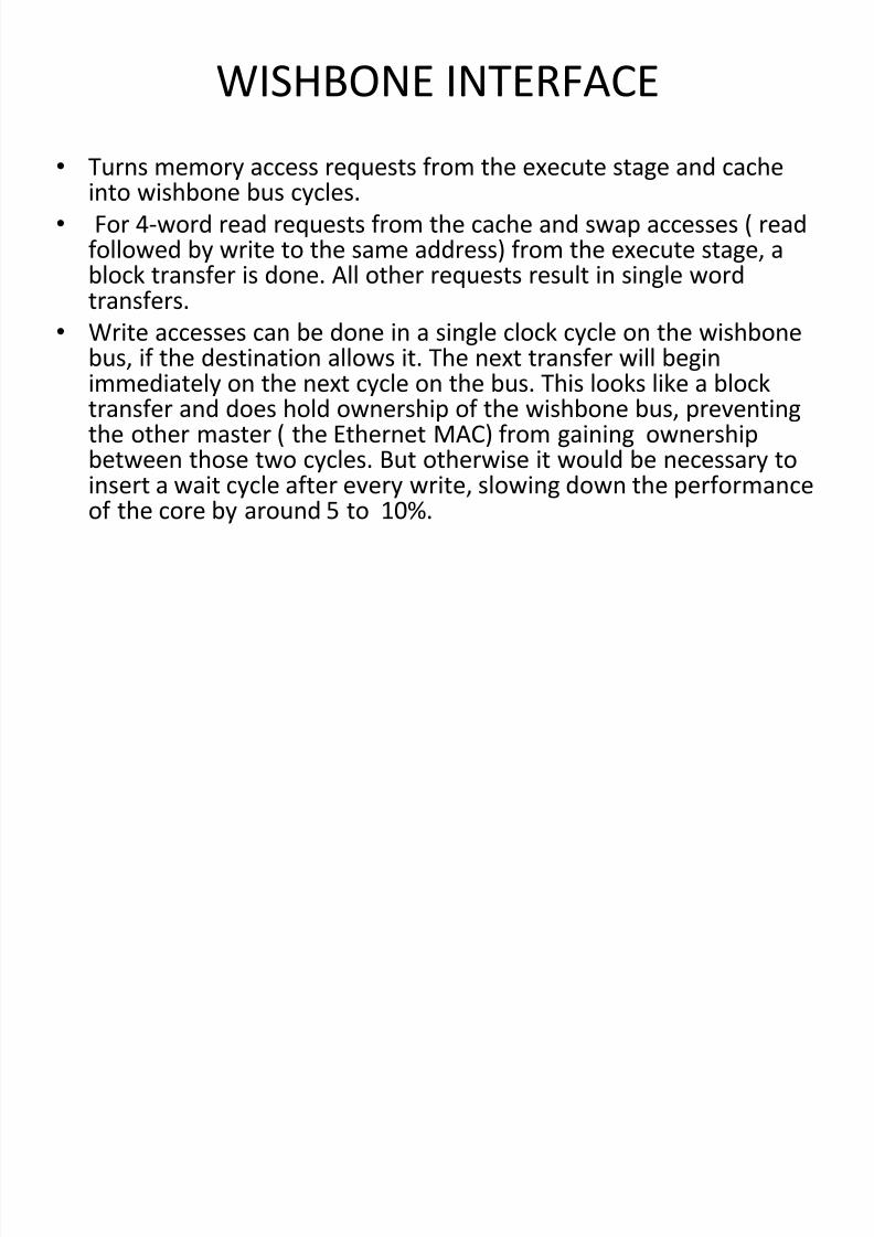
WISHBONE INTERFACE
• Turns memory access requests from the execute stage and cacheinto wishbone bus cycles.
• For 4-word read requests from the cache and swap accesses ( readfollowed by write to the same address) from the execute stage, ablock transfer is done. All other requests result in single word
transfers.• Write accesses can be done in a single clock cycle on the wishbone
bus, if the destination allows it. The next transfer will beginimmediately on the next cycle on the bus. This looks like a blocktransfer and does hold ownership of the wishbone bus, preventingthe other master ( the Ethernet MAC) from gaining ownership
between those two cycles. But otherwise it would be necessary toinsert a wait cycle after every write, slowing down the performanceof the core by around 5 to 10%.

7/31/2019 Main Part of Ppt
http://slidepdf.com/reader/full/main-part-of-ppt 6/19
DECODE
• Decode - The instruction is received from the
fetch stage and registered. One cycle later it is
decoded and the datapath control signals
prepared for the next cycle. This stage
contains a state machine that handles multi-
cycle instructions and interrupts

7/31/2019 Main Part of Ppt
http://slidepdf.com/reader/full/main-part-of-ppt 7/19

7/31/2019 Main Part of Ppt
http://slidepdf.com/reader/full/main-part-of-ppt 8/19
EXECUTE
• The control signals from the decode stage are
registered and passed into the execute stage,
along with any read data from the fetch stage.
The operands are read from the register bank,
shifted, combined in the ALU and the result
written back. The next address for the fetch
stage is generated.

7/31/2019 Main Part of Ppt
http://slidepdf.com/reader/full/main-part-of-ppt 9/19
REGISTER BANK

7/31/2019 Main Part of Ppt
http://slidepdf.com/reader/full/main-part-of-ppt 10/19
MUL UNIT
• 64-bit Booth signed or unsigned multiply and
multiply-accumulate supported. It takes about
38 clock cycles to complete an operation

7/31/2019 Main Part of Ppt
http://slidepdf.com/reader/full/main-part-of-ppt 11/19
The Booth's algorithm
Multiplier logic circuit

7/31/2019 Main Part of Ppt
http://slidepdf.com/reader/full/main-part-of-ppt 12/19
BARREL SHIFTER• Provides 32-bit shifts LSL, LSR, ASR and ROR

7/31/2019 Main Part of Ppt
http://slidepdf.com/reader/full/main-part-of-ppt 13/19

7/31/2019 Main Part of Ppt
http://slidepdf.com/reader/full/main-part-of-ppt 14/19
ALU

7/31/2019 Main Part of Ppt
http://slidepdf.com/reader/full/main-part-of-ppt 15/19
The following table describes these control signals.
ALU Function Encoding
Field Function
swap_sel Swaps the a and b inputs
not_sel Selects the NOT version of b
cin_sel[1:0]
Selects the carry in to the full added from { c_in, !c_in, 1, 0 }. Note that bs_c_in is the
carry_in
from the barrel shifter.
cout_sel Selects the carry out from { full_adder_cout, barrel_shifter_cout }
out_sel[2:0
] Selects the ALU output from { 0, b_zero_extend_8, b, and_out, or_out, xor_out,
full_adder_out }

7/31/2019 Main Part of Ppt
http://slidepdf.com/reader/full/main-part-of-ppt 16/19
Branch and Branch with link (B, BL)
• Branch instructions contain a signed 2's
complement 24 bit offset
• The instruction can therefore specify a branch
of +/- 32Mbytes
• Branch with Link (BL) writes the old PC into
the link register (R14) of the current bank

7/31/2019 Main Part of Ppt
http://slidepdf.com/reader/full/main-part-of-ppt 17/19
Data processing
• The first operand is always a register (Rn). The
second operand may be a shifted register (Rm)
s bit indicate whether to update status flags
in PC register or not.
• Certain operations (TST, TEQ, CMP, CMN) do
not write the result to Rd. They are used only
to perform tests and update flags so S bit is 1.

7/31/2019 Main Part of Ppt
http://slidepdf.com/reader/full/main-part-of-ppt 18/19

7/31/2019 Main Part of Ppt
http://slidepdf.com/reader/full/main-part-of-ppt 19/19
Shift
• When the second operand is specified to be a shifted register, the Shift
field in the instruction controls the operation of the barrel shifter. This
field indicates the type of shift to be performed (logical left or right,
arithmetic right or rotate right). The amount by which the register should
be shifted may be contained in an immediate field in the instruction, or in
the bottom byte of another register (other than R15).