major trends in gravure printed electronics
TRANSCRIPT
Major Trends in Gravure Printed ElectronicsBy Donna Ariel Clark
Graphic Communication DepartmentCollege of Liberal Arts
California Polytechnic State UniversityJune 2010
© 2010 Donna Clark
Abstract
Printing has become a mature industry, forcing printers to create new applications
for their manufacturing process. One such application is printed electronics. The
gravure printing process allows for incredible speed and exceptional quality for tra-
ditional graphic printing. Theoretically, this would be an ideal method for the com-
mercial production of printed electronics. This study analyzes gravure’s capabilities
to produce a uniform conductive ink line and what to expect in the future of gravure
printed electronics. Printed line properties such as line widening and scalloped
edges were determined to impede gravure’s ability to lay down a conductive ink
line. Best results were achieved with high viscosity inks, high pressure, and a slow
printing speed. Ink surface uniformity was also a problem due to ink dots created
from the electromechanically engraved cells, thus increasing line resistance. In gen-
eral, the gravure process needs to be substantially modified before a mass production
of printed electronics can take place. Although it is unlikely that any specific printing
process, will completely dominate the production of a single electronic product, gra-
vure will be substantial portion of a hybrid electronic manufacturing process. Pos-
sible applications include low power devices, such as batteries or photovoltaics.
Table of Contents
Chapter 1: Introduction 4
Chapter 2: Literature Review 7
Chapter 3: Research Methods 15
Chapter 4: Results 19
Chapter 5: Conclusions 28
References 30
Chapter 1 Introduction
4
Printed electronics is a new market for the graphic communication industry. Pair-
ing traditional printing processes with conductive, metal-based inks allows for the
production of electrically functional devices, known as printed electronics. Modi-
fying traditional printing processes is a cost-efficient way to mass produce simple
electronic devices. Printed electronics can be created using several of traditional print
processes including screen printing, flexography, offset lithography, gravure, and
inkjet. Each process has its own strengths and limitations in regard to the production
of printed electronics, allowing each process to be the ideal method of production for
a different range of products or layers.
Huge growth is expected in the market for printed electronics. Currently, applica-
tions for printed electronics include flexible displays, smart labels, photovoltaic
devices, organic light emitting diode (OLED) displays, electronic memory and logic,
and radio frequency identification (RFID) tags. For electronics to be printed suc-
cessfully, high resolution is crucial. High resolution corresponds with high-quality
graphics. With traditional printing, the human eye determines the quality of the
printed piece. Microscopic gaps in ink flow are not an issue, as they are not visible to
the viewer. However, when printing some electronics, resolution is an essential part
of the structure and function of the printed piece. Continuous lines of metal-based
ink are needed for conductivity and to ensure continuity throughout a circuit.
Electrical current is the rate of flow of electrons moving through an electrical conduc-
tor. These electrons carry an electrical charge. Solid, conductive metals, such as gold,
5
copper and silver, contain free electrons. When an electrical force is placed on a
conductive metal wire, the free electrons move in the direction of the force, creat-
ing an electrical current. The resistance of the electrical current depends on the
thickness and length of the wire. In print, this translates to the width, ink height
and length of the printed line. Thicker wires and longer wires allow for more
substantial electric currents to flow through them.
The gravure printing process has the ability to produce extremely high qual-
ity images, and is the most cost-effective way to print long-run jobs among the
other methods of commercial printing. Some common gravure printed products
include wood laminates, printed flooring, wrapping paper, and high quality
publications such as National Geographic. In gravure, a large steel cylinder is
electroplated with copper and engraved with microscopic cells using either elec-
tromechanical or laser engraving. The cylinder is then electroplated with chrome
to ensure that it will not wear down during print production. Low viscosity, or
fluid, ink is held in a bath beneath the rotating gravure cylinder, filling the etched
cells with ink. A blade is then used to scrape off any excess ink from the cylinder
as it rotates. A roll, or web, of paper travels between the etched cylinder and an
impression cylinder, using capillary action to transfer the ink from the cells onto
the paper. In several cases, a process called electrostatic assist is used, where
an electrostatic charge is added to the paper to help ensure that all of the ink is
extracted from the cells on the etched cylinder and transferred to the substrate.
Gravure has the capability to print a continuous image, allowing it to be a versa-
tile printing process.
Using gravure for printing electronics is a cost-effective way to produce a large
quantity of functional electronic devices. While still in its infancy, gravure print-
6
ed electronics have the potential to become a major asset in the marketplace. This
study asks the question: What are the major trends in gravure printed electronics?
Companies are continuing to experiment with electronic applications that would
be best suited for gravure printing, and several innovative ideas are beginning to
emerge.
The future of gravure printed electronics most likely lies in the market for organic
semiconductors and batteries. Organic semiconductors are used in the production of
flexible LEDs and photovoltaics. While gravure is capable of printing extremely high
quality graphics, it struggles to produce consistent straight lines. A large degree of
control is needed over the size and shape of lines printed with conductive ink. The
applications for gravure printed electronics might be limited due to this production
constraint. Both the production of photovoltaics and batteries require a large-ink lay
down to create a working product, which is a strength of the gravure process.
The purpose of this study is to determine the potential for printed electronics by the
gravure printing process. Specific thicknesses of ink are needed for different amounts
of electrical current to pass through conductive printed lines. Ink-height and width
capabilities will be analyzed to determine if the gravure process is viable method
for producing low frequency printed electronics, and to specify which applications
gravure is best suited for.
7
Chapter 2 Literature Review
The gravure printing process is a cost-effective way to print long-run, high-quality
jobs. Chrome-plated etched cylinders do not wear out as quickly as other forms of
printing plates, so long-run jobs of over a million copies are possible without reim-
aging the cylinder. Gravure allows for the use of a variety of substrates, including
thin films. The process is also capable of accepting a range of ink viscosities and can
directly apply a variable ink film thickness to the substrate. This versatility allows
gravure to be a preferable method for printing electronics. As the market for printed
electronics expands, gravure technology also continues to advance and adapt to meet
the needs of the market.
Gravure versus Inkjet Printing Technologies
Inkjet printing is currently the most studied form for producing lost-cost printed
electronics. Inkjet printers include an inkjet head with many nozzles connected to a
separate ink cartridge. These printers use a drop-on-demand technique where each
nozzle moves back and forth depositing drops of ink that are about 50 microns wide
(50 millionths of an meter) onto the substrate (Lawler). There are two types of drop-
on-demand inkjet printers: thermal, or bubble jet, and piezoelectric. Thermal inkjet
printers deposit ink from the nozzle by heating the ink until a bubble is formed, thus
forcing a small drop of ink out from the nozzle. Piezoelectric inkjet printers use an
electric charge which causes a piezo crystal to expand and change shape, pushing a
droplet of ink out of the nozzle (Lawler).
While inkjet printers are ideal for researching printed electronics, their slow speed
8
inhibits the process from being used as a high-volume, industrial production method
for printed electronics. In a technical report published by the University of California,
Berkeley entitled Gravure as an Industrially Viable Process for Printed Electronics;
Donovan Sung notes the advantages and drawbacks of printing electronics via inkjet.
Despite the promising results, inkjet printing has a number of disad
vantages which prevent it from becoming an industrial production
technique for printed electronics. First, it has a low throughput be
cause of its slow print speed. Each ink droplet must be individually
deposited through a printing dispenser, as opposed to roll-to-roll
printing techniques where multiple drops can be printed at the same
time. Second, inkjet printing tends to have short run lengths because
the print heads are subject to clogging. Third, it cannot easily print a
wide range of ink viscosities, which is necessary to properly optimize
printed lines. Finally, it has a certain level of process instability be
cause of statistical variation of droplets (Sung, 3).
While inkjet printing is a useful and cost effective way to print a small production of
printed electronics, it simply cannot keep up with the speed and versatility of other
commercial printing methods (Sung, 3).
For the mass production of printed electronics, gravure excels in the areas where
inkjet falls short. Large gravure cylinders are capable of printing up to 2000 feet per
minute while simultaneously depositing multiple drops of ink at a time, where an
inkjet head prints one drop at a time (Sung, 4). Also, the cells on an etched gravure
cylinder are constantly refilled with ink as the cylinder rotates within the ink trough
below, thus sustaining long print runs and preventing against ink clogging, which
is a common problem with the inkjet process. Gravure is also capable of printing a
relatively wide variety of ink viscosities, or thicknesses of ink. Traditional gravure
9
printing yields excellent quality and micro-engraving and micro-gravure printing are
capable of an extremely high resolution, or very detailed product, necessary for high
density circuits (Daetwyler). Gravure is mechanically simple process with fewer vari-
ables to control compared to other commercial printing methods, generally leading
to a more consistent image (Sung, 5). These characteristics also help gravure compete
against other high-speed printing processes such as lithography, flexography, and
screen printing.
Controlling Gravure Quality
The quality of gravure is affected by several variables such as substrate properties,
ink properties, and other mechanical parameters. Substrate properties and ink prop-
erties can have a large effect on the quality of the ink transferred. Substrate proper-
ties include smoothness (the flatness of the paper), compressibility (how much the
paper compresses between rollers), porosity (a ratio of the volume of pores in the pa-
per compared to the total mass), ink receptivity and wettability (how well the paper
absorbs ink). Ink properties include ink chemistry (the chemical make-up of the ink),
viscosity (the ink’s resistance to flow), solvent evaporation rate (how quickly solvent
evaporates from within the ink), and drying. Parameters of the gravure process also
effect print quality, such as doctor blade angle and pressure, impression pressure,
printing speed and the uniformity of the gravure cylinder diameter (Hrehorova, Kat-
tumenu).
Cylinder Engraving Methods
When printing gravure, three different engraving methods can be used. These meth-
ods include electromechanical engraving, direct laser engraving and chemical etch-
ing with laser ablation. Each engraving method can produce various shapes and
dimensions of gravure cells (Hrehorova, Kattumenu).

10
Electromechanical engraving is currently the most widely used engraving method. A
diamond stylus is used to cut gravure cells directly into the copper cylinder as it ro-
tates. Usually, one oscillation of the stylus produces one cell, and the volume of that
cell depends on the amplitude of the oscillation, which is limited by the mechanical
resonance of the stylus holder (Hrehorova, Kattumenu). Different tonal values are
produced by engraving cells of various volumes. However, cells are limited to a fixed
aspect ratio defined by the geometry of the diamond stylus. To produce lines, a row
of dots is etched into the cylinder; therefore it is common to see ragged edges with
electromechanical engraving (Hrehorova, Kattumenu).
In contrast, direct laser engraving does not involve a mechanical stylus at all. A laser
beam is focused onto the surface of the gravure cylinder to create cells. Typically, gra-
vure cylinders are coated with copper, but copper does not absorb laser energy, so a
zinc layer is added to the surface of the cylinder for engraving purposes (Hrehorova,
Kattumenu). Each pulse creates one cell and the cell volume is determined by the
energy of that pulse. Direct laser engraving allows for a free selection of cell dimen-
sions which helps to optimize ink transfer to the substrate (Hrehorova, Kattumenu).
Chemical etching in the final method used for cylinder engraving. Laser technology
is also used in this process by imaging the mask layer, or creating what area will be
engraved, prior to chemical etching. In the past, gravure was based on a film analog
exposure and developing of the mask layer followed by chemical etching. Today,
laser ablation is used, so no developing is needed (Hrehorova, Kattumenu). The
amount of time that the etchant is in contact with the copper surface of the gravure
cylinder controls the cell depth. In general, each cell produced has the same depth,
so tonal variation is achieved by controlling the diameters of the etched cells (Hreho-
rova, Kattumenu).
11
For direct laser engraving and chemical etching with laser ablation, the resolution of
engraving is limited by the diameter of the laser beam focus.
With a direct laser imaging system, a minimum beam size of about
40 microns, [or 40 millionths of a meter], is used and, therefore, the
minimum line width is about 40 microns. Indirect laser systems use a
laser beam split into four beams of equal power (sufficient to ablate
the mask resist) and typically work with a beam diameter of 10-20
microns for gravure applications. The minimum line width is, there
fore, also about 10-20 microns, or a little more due to the sidewall etch
ing (Hrehorova, Kattumenu).
This allows for a much thinner line to be printed if chemical etching with laser abla-
tion is used. The capability of printing such thin lines makes gravure a viable method
for the mass production of printed electronics (Hrehorova, Kattumenu).
Consistency of Ink Lines
While the gravure process is known for superior image quality, the etched cells
struggle to produce a consistent ink line. The main challenge for gravure printed
electronics is producing extremely thin lines accurately, which can be necessary for
the electrical function of the printed device. Some electronic structures require con-
ductive lines less than 20 microns wide (Sung, 26). There are two methods in gravure
for printing solid lines: printed gravure lines, where a series of separate cells are
etched closely together to form lines, or intaglio trenches, where a continuous trench
is etched into the gravure cylinder. In his technical report, Donovan Sung evaluated
the usability of both cells and trenches for printing small conductive lines (Sung, 26).
Printed gravure lines can show three types of printed line behavior. First, the drops
can spread far enough apart to form discrete dots. Second, ink dots only partially in-
12
tersect, resulting in “scalloped” or “saw-toothed” lines that can be narrower than the
width of the individual drops. Lastly, the individual drops can form a smooth and
continuous line. This can occur when the spacing between the cells is optimized, or
when the ratio of drop spacing to landed drop radius is 1:10. The drop spacing is the
distance between the centers of neighboring drops (Sung, 24).
Intaglio trenches are another method that can be used in gravure to print continuous
lines. They remove the need of optimizing drop spacing and drop radius and can
theoretically be scaled down to very small cell widths without worrying about cell
emptying (Sung, 34). Intaglio trenches do have one very important defect that should
not be overlooked. Trenches that are etched parallel to the print direction often show
a “pick out” effect, meaning that the ink simply never transfers to the paper or sub-
strate. However, pick out does not occur in trenches that are etched horizontally to
the printing direction. Research suggests that this is because of the fluid flow within
the trenches (Sung, 34). Overall, intaglio trenches have a greater variation in printed
width uniformity compared to gravure printed lines, and typically print much wider
lines. When the trench width is decreased, the printed line width only slightly de-
creases and can never reach a width of less than 20 microns, needed for some forms
of printed electronics. Therefore, the best method for printing solid, narrow and con-
tinuous lines in gravure is to print individual cells with appropriate spacing (Sung,
35).
Electrical Resistance and Ohm’s Law
Although the consistency of ink lines is important for conducting electrical current;
the length, width and height of the ink line also need to be controlled to support the
flow of electrons throughout the ink line. In electricity, resistance is a property of
an electrical conductor where it opposes the flow of electrons (Columbia Electronic
13
Encyclopedia). Voltage is described as the difference in potential energy between any
two points in a circuit (Johnson, Roberts).
Ohm’s Law states that the electric current (i) is equal to the applied voltage (v) divid-
ed by the resistance (r), or i = v/r (Columbia Electronic Encyclopedia). The resistance
of electrical conductors can be controlled by three factors, conductor length, width,
and height. Two wires, or in the case of printed electronics, conductive ink lines, that
all have the same width and height can vary in resistance according to their length.
The longer wire, or ink line, will have a greater resistance. If two wires, or ink lines,
are of the same length, the resistance decreases as the thickness increases (thickness
= length x width). In other words, thicker wires, or ink lines, allow more electrons to
flow through them, thus the electrical current is increased (Johnson, Roberts).
Developments in Printed Electronics
Several new developments are occurring in the market and technology for printed
electronics. Such developments include the use of mixed printing technologies, ad-
vancements in organic light emitting diodes (OLED) and radio frequency identifica-
tion (RFID) tags, and the continued experiments with copper and other conductive
inks (Harrop).
The employment of mixed printing technologies when producing printed electron-
ics is becoming increasingly popular. These include combinations of micro-gravure,
screen and ink-jet printing. New developments in toys and Internet interactive gam-
ing cards make the use of screen printed electrodes and gravure printed ferroelectric
memory polymers (Harrop).
Kodak holds the majority of patents on the latest OLED materials (Harrop). OLEDs
are a thin and light display technology that does not require backlights. AMOLED,
14
or active matrix organic light emitting diodes, are being experimented with for the
use in large to medium displays including televisions (Harrop). Takatoshi Tsujimura,
Senior Director of OLED Product Development for Kodak Japan Ltd concludes that
medium to large AMOLED displays can be made by a combination of low risk tech-
nologies (Harrop).
Sunchon University in Korea has had great success in printing complete RFID tags
using regular printing equipment. RFID tags can be used in products, animals, or
even people for identification and tracking. A large market is seen in retail for inven-
tory purposes. Sunchon University’s RFID tags use inorganic semiconductors and
dielectrics. To reduce cost, paper substrates are beginning to be of interest (Harrop).
With the expensive price of silver, other conductive metals need to be used as viable
ingredients for metal based inks. Copper based inks are an option, though the corro-
sion on the copper poses a challenge. Hitachi Chemical has also announced organic
insulating inks, suitable for printing resistors (Harrop).
Summary
Developments in printed electronics are opening new markets for traditional print-
ing processes. While inkjet printing is currently used most frequently for the testing
of printed electronics, gravure has more potential to become a means of production
for the mass production of printed electronics. The quality of gravure printing can
be affected by several variables, but many techniques can be used to control quality
such as engraving techniques and optimizing the drop spacing ratio. Electrical resis-
tance must also be taken into account for the conducting of electrical current within
gravure ink lines. Gravure is an ideal production method for large quantities of
high quality prints. Theoretically, gravure’s ability for extremely fast, high resolution
printing makes it an ideal candidate for the mass production of printed electronics.
15
Chapter 3 Research Methods
Certain variables may have an effect on the electrical function of printed electronics.
This study is specifically interested in the capabilities of the gravure printing process
to print conductive ink lines and the factors effecting how these lines are produced,
as well as the applications that gravure would be best suited to manufacture. Two re-
search methods were used to complete this study including secondary research and
elite and specialized interviewing.
Secondary research involves analyzing previously published studies and literature to
gain a better understanding of the topic being analyzed. The researcher must locate,
gather, and interpret facts from previously published information and attempt to
draw conclusions about the research subject.
Elite and specialized interviewing requires the interviewer to ask precise, open-
ended questions, allowing the interviewee to establish a perspective on the subject.
This type of interviewing allows for different responses between interviewees as
comprehensibility, plausibility and consistency is sought, rather than a duplication
of responses. It is best not to have a prepared list of questions or take notes during
the interview, but rather record the interview to allow conversation to flow naturally
while still capturing all of the relevant information (Levenson, 22-23).
By using secondary research, one aims to understand gravure’s capabilities of print-
ing conductive ink line. Past research projects and literature were analyzed to deter-
mine the capabilities of gravure ink lay-down and how the gravure process affects
16
the electrical current of printed electronics.
One of the documents that was reviewed was a study undertaken by the Center of
Ink and Printability Research at Western Michigan University. The study was pub-
lished in GravurEzine in March 2009 and titled Gravure Printed Features for Printed
Electronics. In this study, Alexandra Pekarovicova, Erika Hrehorova, Paul D. Fleming,
Marian Rebros, and Margaret K. Joyce modify a flexographic press to print in a gra-
vure configuration, and use this press to research gravure printed electronics.
Another document that was reviewed was a technical report from the Electrical Engi-
neering and Computer Sciences Department of the University of California, Berkeley
titled Roll Printed Electronics: Development and Scaling of Gravure Printed Techniques. In
December 2009, Alejandro De la Fuente Vornbrock designed a custom table-top gra-
vure press to make laboratory testing possible and cost-effective.
Two studies from the University of Oulu in Finland were also examined. The first
was titled Gravure Printing of Conductive Particulate Polymer Inks on Flexible Substrates
by Marko Pudas, Niina Halonen and Jouko Vähäkangas from Microelectronics and
Physics Laboratories in 2005. In this study, the roto-gravure process was used and
conductor line qualities were characterized for different substrates. The qualities in-
clude resistance, yield as a function of line width, coil inductance, folding endurance,
adhesion, printed antenna properties and maximum current density.
The second study from the University of Oulu in Finland was titled Gravure Offset
Printing of Polymer Inks for Conductors. In 2003, as part of the Microelectronics Labora-
tory and EMPART Research Group of Infotech Oulu, Marko Pudas, Juha Hagberg,
and Seppo Leppävuori studied ink curing, or drying, and electrical properties of
polymer inks that were printed using a gravure press.
17
Elite and specialized interviewing was also be used as a research method. Two pro-
fessors within the graphic communication department at Cal Poly have been in-
volved in research in the field of printed electronics: Dr. Xiaoying Rong and Dr. Mal-
colm Keif. Both of these professors were questioned to establish the major trends that
are emerging in gravure printed electronics. Questions for the interviewees included:
• What is your area of study within printed electronics?
• How do you believe that gravure will impact the field of printed elec-
tronics in the future?
• What properties of gravure do you feel will help or impede the use of
gravure for production of printed electronics?
• What specific electronic products do you believe that gravure would be
an ideal production method for?
These questions were aimed at understanding the print side of printed electronics as
well as seeing where the gravure fits into the printed electronics world.
A professor from Cal Poly’s Electrical Engineering department, David Braun was
also interviewed to determine the structural characteristics necessary to print a prod-
uct that is capable of conducting electricity. Professor Braun has been researching
new applications for organic semiconducting polymers. Questions for the interview-
ee included:
• What are the basic structural characteristics needed for an electrical de-
vice?
• Would you explain Ohm’s Law, and how that might affect conductive ink
that is printed on a flexible substrate?
• What is an IR drop, and how does it affect electrical current?
• What do you see happening in the future for printed electronics?

18
After performing secondary research and elite and specialized interviewing, the
results of the research were explored. Capabilities of gravure ink lay-down were
examined to determine the effect on the production of a conductive ink line and the
products that gravure is best suited to produce. Conclusions were drawn exploring
the possibilities for gravure in the future of printed electronics.

19
Chapter 4 Results
Research Study: Gravure Printed Features for Printed Electronics
In the study Gravure Printed Features for Printed Electronics, researchers from Western
Michigan University tested three different types of gravure configurations; offset
gravure, direct gravure with an open pan and inking roll, and direct gravure with an
enclosed doctor blade chamber. Two conductive inks were used including a nanopar-
ticle silver gravure ink and a water-based silver flake ink. Both were printed on
commercial label paper as well as 2µm (2 microns) thick polyethylene terephathalate
(PET) film.
The three gravure configurations produced very different results. When the meter-
ing roll with open inking pan was used, premature evaporation of the ink was no-
ticed, requiring ink viscosity to be constantly adjusted by the addition of solvent. In
the enclosed direct gravure configuration, some ink dots were missing and were not
successfully transferred to the substrate. With the offset gravure process, all ink dots
were transferred but many showed a distorted shape.
In the attempt to print a 40µm wide line, the effect of impression pressure was tested
among the gravure configurations. Direct gravure produced the best fidelity of line
width, and offset gravure produced the worst. When the highest impression pressure
was used, all gravure configurations experienced line widening. The results of the
printed line width and percent gain for each process are shown in Table 1.
20
Table 1: Line Widening of a 40µm Line
Printed Line Width Percent Gain
Offset Gravure 98±8µm 145%
Direct Gravure 62±4µm 55%
Other factors such as ink viscosity and print direction were shown to have an effect
on line fidelity. Higher ink viscosity combined with high impression pressure result-
ed in the best line width (50.7±4µm for a 30µm nominal line). Lines printed parallel
to the print direct showed better line fidelity than those printed perpendicular to the
rotating cylinder.
Research Study: Roll Printed Electronics: Development and Scaling of Gravure Print-
ing Technologies
This study was conducted by the University of California, Berkeley in the Electrical
Engineering and Computer Sciences department. Alejandro De La Fuente Vornbrock
examined the differences between printing dots, gravure-patterned lines and intaglio
trenches with several types of conductive inks. A print speed of 0.1m/s was used to
help maintain a stable printing process. All samples were printed on polyethylene
terephthalate (PET).
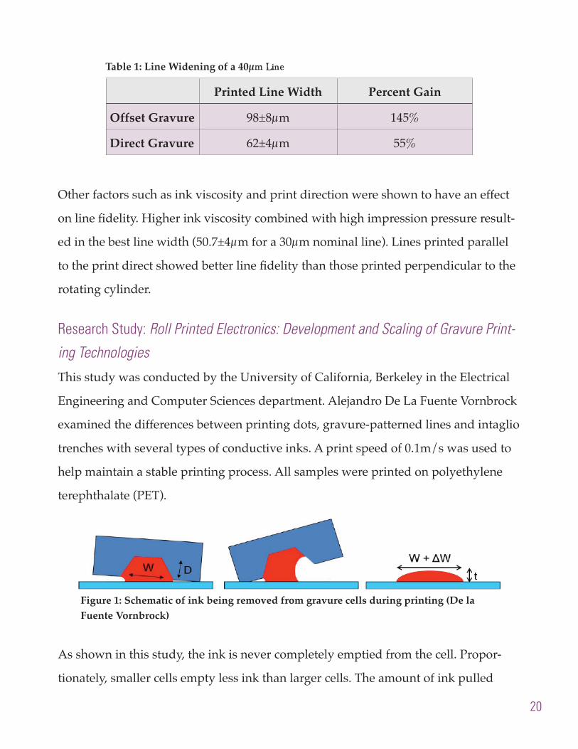
As shown in this study, the ink is never completely emptied from the cell. Propor-
tionately, smaller cells empty less ink than larger cells. The amount of ink pulled
Figure 1: Schematic of ink being removed from gravure cells during printing (De la Fuente Vornbrock)
21
from the cell can be affected by the surface energy of the substrate. Substrates with
higher surface energy tend to adhere better to the ink causing more complete cell
emptying. Print speed also affects cell emptying, as it determines how much sheer is
applied to the ink. At high printing speeds, inks with higher viscosity have a greater
resistance to sheer, causing cell-emptying problems.
This study also showed the effects of viscosity on line quality. If ink is too viscous,
ink drops will result in lines with poor uniformity of width and thickness. Low vis-
cosity inks can create lines that are too thin to be conductive. Optimizing ink viscos-
ity helps to create thin, uniform, and straight lines with maximum thickness. Usually,
wider lines tend to produce more uniform print thickness, because they allow more
time for capillary flow, giving the individual drops time to smooth out.
22
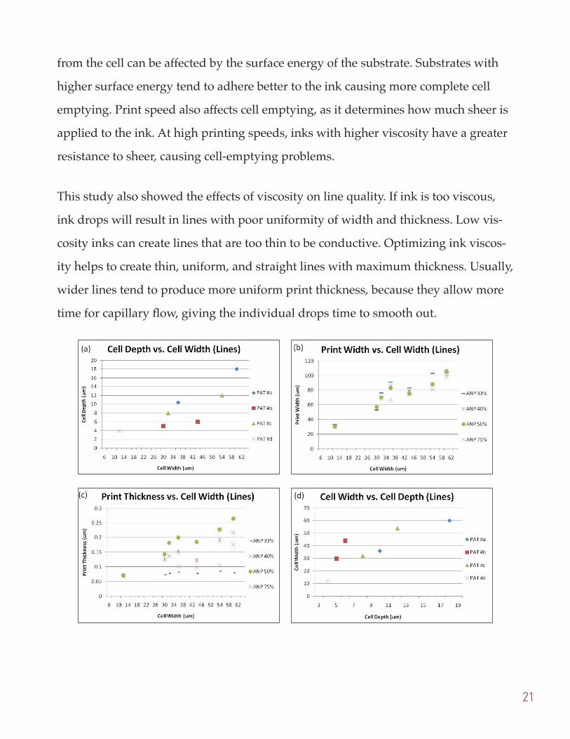
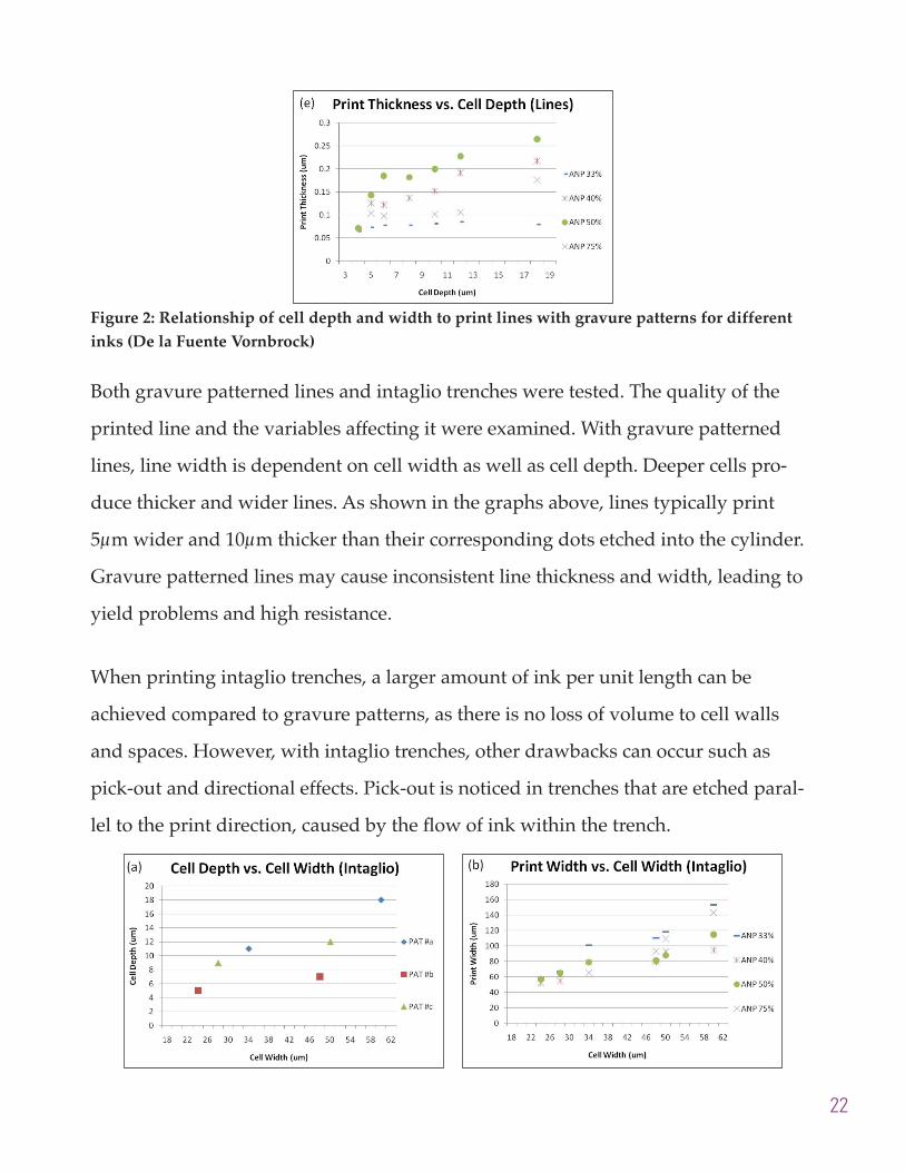
Both gravure patterned lines and intaglio trenches were tested. The quality of the
printed line and the variables affecting it were examined. With gravure patterned
lines, line width is dependent on cell width as well as cell depth. Deeper cells pro-
duce thicker and wider lines. As shown in the graphs above, lines typically print
5µm wider and 10µm thicker than their corresponding dots etched into the cylinder.
Gravure patterned lines may cause inconsistent line thickness and width, leading to
yield problems and high resistance.
When printing intaglio trenches, a larger amount of ink per unit length can be
achieved compared to gravure patterns, as there is no loss of volume to cell walls
and spaces. However, with intaglio trenches, other drawbacks can occur such as
pick-out and directional effects. Pick-out is noticed in trenches that are etched paral-
lel to the print direction, caused by the flow of ink within the trench.
Figure 2: Relationship of cell depth and width to print lines with gravure patterns for different inks (De la Fuente Vornbrock)

23
Figure 3: Relationship of cell depth and width to print thickness for intaglio trenches for differ-ent inks ( De la Fuente Vornbrock)
The figure above shows the relationship between intaglio depth and width compared
to print width and thickness. The relationship is linear with a dependence on cell
depth. The print thickness is also linearly dependent on cell depth with a small cor-
relation to cell width. Generally, intaglio trenches print wider lines than those pro-
duced by gravure patterned lines.
Research Study: Gravure Printing of Conductive Particulate Polymer Inks on Flexible
Substrates
In this study, researchers from the University of Oulu, Finland, printed gravure test
patterns of high-conductivity inks containing particles of silver to determine resis-
tance with different line widths and lengths. For comparison, similar patterns were
printed by a rotary-screen process. Chemical etching was used to create 20-60µm
deep grooves into the cylinder. This study determined that the maximum line ink
24
cross-section is not the best measurement of a conductor, but rather the line cross-
section averages give a better indication of conductivity.
When using printing methods, maximum conductivity can be difficult to achieve.
For high conductivity, a thick ink layer is needed. This can be obtained with high
viscosity and a silver content up to 80%. However, specifications for gravure printing
require a lower ink viscosity and a higher solvent content, allowing silver content to
be only as high as 60-70%.
During testing, the 20-60µm deep grooves produced ink lines that were 4-7µm thick.
For printing the thickest ink layer, high pressure and a slow printing speed are pre-
ferred. Although more ink is printed from wider grooves, significant line widen-
ing occurs as the ink spreads, causing a disadvantage. Both intaglio trenches and
gravure-patterned lines were tested in this study. A lower resistance and a thicker ink
later was seen in the intaglio trenches.
Research Study: Gravure Offset Printing of Polymer Inks for Conductors
Researchers from Oulu, Finland used offset gravure in this study. The gravure
grooves were used to transfer the ink to a pad, and the pad was used to transfer the
ink to the substrate. The goal of the experiment was to decrease the resistance of con-
ductor lines.
Two inks, ink A and ink B, were tested, with ink B having a higher solid particle con-
tent. Ink A had a high viscosity and dried very rapidly, causing the ink to block the
grooves in the gravure cylinder. Oil was added to the ink, improving printability but
decreasing the highest ink laydown. The printing environment was altered in order
to achieve the best printing parameters possible for the inks to be studied.

25
During testing, a minimum square resistance of 20mΩ/square was achieved for a
300µm wide line and a square resistance of 28mΩ/square was achieved for a 150µm
wide line. Both lines were between 7-8.5µm thick.
Personal Interview: Dr. Xiaoying Rong
Dr. Xiaoying Rong explained her opinion on gravure process capabilities for printed
electronics and the future gravure has in the market. Dr. Rong has been specifi-
cally doing research with screen printed electronics, but the coarse resolution of the
screens makes printing devices with fine features impossible. Dr. Rong explained
issues concerning ink surface uniformity. With any printing process, ink film is ex-
pected to level out, but sometimes due to the formulation of the ink, a lack of surface
uniformity is produced. With gravure, peaks and valleys are noticed on the surface
of the ink due to the cells on the gravure cylinder that carry the ink. This can cause
problems with electrical resistance. In order to achieve a thick ink film, sometimes
several layers need to be printed on top of underlying layers. This “double hit” of
ink increases problems with surface uniformity.
Dr. Rong believes that all types of electronics cannot be achieved through printing
methods. It is unlikely that high power devices will be manufactured on a printing
press. Currently, the demand for printed electronics is not very high, so a slower
speed will suffice. Gravure strengths compared to other printing processes are in
speed and resolution. In the future, Dr. Rong believes that the best option for gra-
vure will be to add function to existing printing. This may include simple electronic
products such as electrolumiescent wallpaper. Also, gravure printed electronics can
be included into “smart packaging” for uses like tracing and detecting. The produc-
tion of transistors or other full-on electronic devices probably won’t happen without
continuous improvement to the process and engraving methods.
26
Personal Interview: David Braun
David Braun is a professor in the Electrical Engineering department at Cal Poly, and
has been doing research with organic light emitting diodes (OLED). Professor Braun
explained that the conduciveness of printed electronics can be limited by the materi-
als resistivity. If the material obeys Ohm’s law, a voltage can be applied and current
measured or a current can be applied and voltage measured. Resistivity and resis-
tance are related but they are not the same thing. Below is an equation showing their
relationship.
Resistance = (resistivity x length)/cross-sectional area
Professor Braun also further commented on Dr. Xiaoying Rong’s concern with rip-
pled ink surfaces. He explained that a thick uniform ink surface would have the low-
est resistance and a thin uniform ink surface would have a higher resistance. How-
ever, a rippled ink surface would cause a resistance even higher than a thin uniform
surface.
Personal Interview: Malcolm Keif
Dr. Malcolm Keif has been studying how printing processes can lay down functional
inks to be useful, including the characteristics of each method and how the ink film it
lays down is characterized. When asked about gravure’s impact on printed electron-
ics, Dr. Keif commented that gravure has the ability to lay down a thick layer of ink.
The biggest advantage that gravure has is the ability to work with a wide range of
ink viscosities. This could allow thicker inks, with better conductive solid densities,
to be used at slow printing speeds. A slower speed is necessary to allow more vis-
cous ink time to enter and be removed from the cell during printing.
Dr. Keif also commented on the drawbacks of gravure for printing electronics, name-
27
ly the electromechanical engraving process. Electromechanical engraving is not good
for engraving sharp edges, and creates serrated edges on printed lines. Typically,
electromechanical engraving changes the cell depth to apply more ink for graphic to-
nality. When printing electronics, a consistent ink film thickness is desirable for both
wide and thin lines. With electromechanical engraving, this would require a consis-
tent cell depth, which is not typically how it’s done. This is not a problem for acid
etching or laser engraving, as cell depth can be controlled.
As for the future of printed electronics, Dr. Keif does not believe that any single
printing process will be good for all functional layers of any product. Everything
will be created from hybrid processes. Gravure’s most likely candidates are batteries,
solar cells, and OLED lighting and signs. These products are the least detailed and
have low power requirements. Dr. Keif has a positive outlook and believes that the
processes that will ultimately “win” in printed electronics haven’t been invented yet,
or at least have not morphed to where they need to be.

28
Chapter 5 Conclusions
After completing the research, it is clear that gravure has many advantages as well as
drawbacks in the production of printed electronics. As a mechanically simple pro-
cess, there are less process variables to control compared to other printing processes.
The use of an etched chrome-plated cylinder lends itself to solvent compatibility,
allowing a broad range of inks to be printed with gravure. Gravure is also capable of
laying down a thicker ink film, necessary for the flow of electrons through conduc-
tive ink.
During the production of gravure printed electronics, several print variables can
affect the fidelity of conductive lines. In general, increased pressure causes line wid-
ening on the substrate. The best line fidelity can be achieved with high viscosity ink,
high pressure, slow print speed, and lines etched parallel to the print direction. The
slow print speed allows time for the ink to fill and be extracted from the cells on the
cylinder, while more viscous ink helps to decrease dot gain and maintain ink height.
Less print problems are seen when lines are etched parallel to the print direction.
One of the most important print variables for printed electronics is ink surface uni-
formity. To create the least resistance through a conductive ink line, a high ink height
is needed with uniform thickness. Printing with gravure patterned lines versus inta-
glio trenches will produce a less uniform ink surface. With gravure patterned lines,
more ink is laid down compared to the same width intaglio trench. The individual
cells create scalloped edges and non-uniform ink surface. As multiple layers of ink
are added, the problem is increased. A wavy ink surface increases the resistance of
29
the printed ink line when compared to a uniform surface.
Printing intaglio trenches instead of gravure patterned lines helps to maintain a more
uniform surface, but other problems are of concern. A severe “pick out” effect can
be observed when intaglio trenches are etched perpendicular to the print direction,
causing gaps in ink flow. This limits the patterns trenches can be etched in to pro-
duce successfully printed lines.
It is unlikely that any specific printing process will completely dominate the pro-
duction of a single electrical product. Gravure will definitely be a large portion of a
hybrid manufacturing process that creates low power devices. Printed electronics
are not going to be high voltage or high density electronics, as the processes are not
capable of printing the small and detailed requirements. Gravure printed electron-
ics will mostly likely include batteries, photovoltaics, and function added to existing
printed products. This may include areas such as smart packaging or electrolumines-
cence products.
As the demand for traditional print declines, printers look for new ways to reinvent
their business. Functional printing will be a part of the future, but it is unlikely that it
will completely transform the way the majority of electronics are manufactured.

References
Braun, David. Personal Interview. May 5, 2010.
Columbia Electronic Encyclopedia, 6th Edition. October 1, 2009. Retrieved online through Academic Search Elite February 17, 2010. <http://search.ebscohost.com/login.aspx?direct=true&db=afh&AN=39025440&site=ehost-live>
Daetwyler R&D Corporation. “Printed Electronics.” Daetwyler R&D Corporation. Retrieved online Janu-ary 31, 2010. <http://www.daetwyler-rd.com/doc/Printed_Elec-tronics_sales-sheet.pdf>
De la Fuente Vornbrock, Alejandro. “Roll Printed Electronics: Development and Scaling of Gravure Printing Technologies.” December 29, 2008. Univer-sity of California Berkeley. Retrieved online March 18, 2010. <www.eecs.berkeley.edu/Pubs/TechRpts/2009/EECS-2009-191.pdf>
Harrop, Peter. “New Trends in Printed Electronics.” Printed Electronics World. October 5, 2009. Retrieved online January 31, 2010. <http://www.printedelectronicsworld.com/ar-ticles/new_trends_in_printed_electronics_00001745.asp>
Hrehorova, Erika, and Ramesh-Chandra Kattu-menu. “Evaluation of Gravure Print Forms for Print-ed Electronics.” GravurEzine. March 2007. Retrieved online January 29, 2010. <http://www.gravurexchange.com/gravurezine/0702-ezine/hrehorova.htm>
Johnson, Phil, and Shaun Roberts. “Electric Cir-cuits.” University of Durham School of Education. 2006. Retrieved online February 17, 2010. <http://www.dur.ac.uk/p.m.johnson/electric_cir-cuits/electric_circuits.htm>
Keif, Malcolm. Personal Interview. May 12, 2010.
Lawler, Brian. “Digital Printing and Emerging Tech-nologies.” April 2009. Class lecture given at Califor-nia Polytechnic State University, San Luis Obispo.
Levenson, Harvey Robert, Ph.D. Some Ideas About Doing Research in Graphic Communication. 2001. Atascadero, CA: The Good Neighbor Press and Services.
Pekarovicova, Alexandra, Erika Hrehorova, Paul D. Fleming, Marian Rebros, and Margaret K. Joyce. “Gravure Printed Features for Printed Electronics.” GravurEzine. March 2009. Retrieved online February 27, 2010. <www.gravurexchange.com/pdfs/GravurE-zine-0902.pdf>
Pudas, Marko, Juha Hagberg, and Seppo Leppävu-ori. “Gravure Offset Printing of Polymer Inks for Conductors.” Progress in Organic Coatings, 49 (4), pp. 324-335. 2004. Retrieved online March 1, 2010. <http://www.sciencedirect.com/science/article/B6THD-4BDC95F-1/2/d8469e89c1e1e8d6d9918e-aff30608c4>
Pudas, Marko, Niina Halonen, Päivi Granat, and Jouko Vähäkangas. “Gravure Printing of Conduc-tive Particulate Polymer Inks on Flexible Substrates.” Progress in Organic Coatings, 54 (4), pp. 310-316. 2005. Retrieved online March 1, 2010. <http://www.gravurexchange.com/gravurezine/0801-ezine/pudas.htm>
Rong, Xiaoying. Personal Interview. May 5, 2010.
Sung, Donovan. “Gravure as an Industrially Vi-able Process for Printed Electronics.” May 23, 2008. University of California Berkeley. Retrieved online January 29, 2010. <http://www.eecs.berkeley.edu/Pubs/TechRpts/2008/EECS-2008-70.pdf>