manual evb jaded interface board version pa4.2 october …€¦ · · 2009-10-28revision date...
TRANSCRIPT

Preliminary1(45)
Prepared Document Number
Manfred OrtmannApproved Checked Date Revision Storage
20091005 PA 4.2 Mycable01
Receiver: Info:M. CarstensBehrens mycable GmbH
Manual
EVB JADED Interface Board
Version PA4.2 October 5, 2009
http://www.fujitsu.com/emea/services/microelectronics

Preliminary2(45)
Prepared Document Number
Manfred OrtmannApproved Checked Date Revision Storage
20091005 PA 4.2 Mycable01
NoticeThe contents of this document are subject to change without notice. Customers are advised to consult with FUJITSU sales representatives before ordering.
Any information in this document, including functional descriptions and schematic diagrams, shall not be construed as license of the use or the exercising of any intellectual property rights, such as patent rights or copyright or any other right of FUJITSU or any third party or does FUJITSU warrant noninfringement of any thirdparty's intellectual property right or other right by using such information. FUJITSU assumes no liability for any infringement of the intellectual property rights or other rights of third parties which would result from the use of information contained herein.
The products described in this document are designed, developed and manufactured for general use, including unrestricted ordinary industrial use, general office use, personal use, and household use but are not designed, developed and manufactured for use accompanying fatal risks or dangers that, unless extremely high safety levels are ensured, could have a serious effect to the public and could lead directly to death, personal injury, severe physical damage or other loss (i.e., nuclear reaction control in nuclear facility, aircraft flight control, air traffic control, mass transport control, medical life support system, missile launch control in weapon systems), or (2) for use requiring extremely high reliability (i.e., submarine or satellite technology). Please note that FUJITSU will not be liable against you and/or any third party for any claims or damages arising in connection with abovementioned uses of the products.
If any products described in this document represent goods or technologies subject to certain restrictions on export under the Foreign Exchange and Foreign Trade Law of Japan, the prior authorization by the Japanese government will be required for export of those products from Japan.
All rights reserved and Copyright © FUJITSU LIMITED 2009
Preliminary3(45)
Prepared Document Number
Manfred OrtmannApproved Checked Date Revision Storage
20091005 PA 4.2 Mycable01
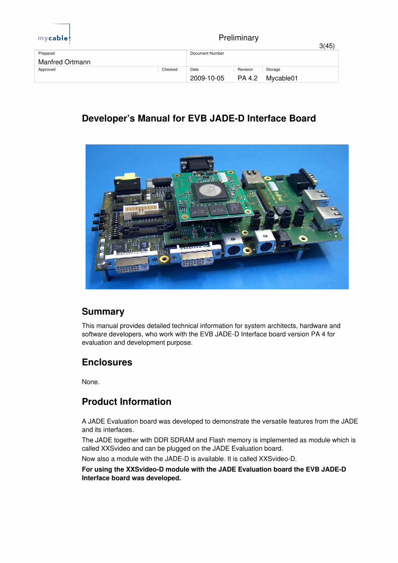
Developer’s Manual for EVB JADED Interface Board
SummaryThis manual provides detailed technical information for system architects, hardware and software developers, who work with the EVB JADED Interface board version PA 4 for evaluation and development purpose.
Enclosures
None.
Product Information
A JADE Evaluation board was developed to demonstrate the versatile features from the JADE and its interfaces.
The JADE together with DDR SDRAM and Flash memory is implemented as module which is called XXSvideo and can be plugged on the JADE Evaluation board.
Now also a module with the JADED is available. It is called XXSvideoD.
For using the XXSvideoD module with the JADE Evaluation board the EVB JADED Interface board was developed.

Preliminary4(45)
Prepared Document Number
Manfred OrtmannApproved Checked Date Revision Storage
20091005 PA 4.2 Mycable01
Revision History
Revision Date Sign Description
PA2.1 20090302 mo Document setup
PA2.2 20090309 mo Pinning of APIX signals
PA3.1 20090423 mo Documentation after finishing PCB
PA3.2 20090515 mo Pin table of X804 added
PA3.3 20090706 mo Pictures added
PA4.1 20090814 mo PCB revision PA4
video connector X804
APIX connector X802
PA4.2 20091005 mo Picture change
Contact Information
mycable GmbHMichael CarstensBehrens( hardware and commercial )
Email [email protected]
Tel. +49 4321 55956 55
mycable GmbHCarsten Schneider ( Software )Email [email protected]
mycable GmbHManfred Ortmann ( Hardware )Email [email protected]

Preliminary5(45)
Prepared Document Number
Manfred OrtmannApproved Checked Date Revision Storage
20091005 PA 4.2 Mycable01
Table of Contents1 OVERVIEW....................................................................................................................6
1.1 Manual Scope........................................................................................................61.2 Putting into Operation.............................................................................................6
2 EVB JADED INTERFACE BOARD...........................................................................7
2.1 System Architecture...............................................................................................72.2 Function Units........................................................................................................9
2.2.1 XXSvideoD Module.....................................................................................102.2.2 XXSvideoD Interface...................................................................................112.2.3 XXSvideo Interface.......................................................................................212.2.4 Configuration................................................................................................302.2.5 ADC Interface...............................................................................................302.2.5 I2C and Host SPI Interface..........................................................................322.2.6 32 bit Flash Memory.....................................................................................332.2.7 USB..............................................................................................................332.2.8 Audio CODEC..............................................................................................342.2.9 APIX.............................................................................................................352.2.10 Video Output..............................................................................................372.2.11 RGB Input..................................................................................................40
2.3 Hardware Variants................................................................................................412.4 Placement of Components...................................................................................422.5 Mechanical Dimensions........................................................................................44

Preliminary6(45)
Prepared Document Number
Manfred OrtmannApproved Checked Date Revision Storage
20091005 PA 4.2 Mycable01
1 Overview
1.1 Manual Scope
This manual provides detailed technical information about the EVB JADED Interface board for system architects, hardware and software developers covering:
• System architecture description and users manual
• Hardware architecture
• Mechanical information
• References to further information like design data, data sheets, software documentation
It is the engineer’s reference for evaluation, system development and prototyping based on the board. This document covers all available hardware versions regarding their configuration options and revision state.
1.2 Putting into Operation
Plug the EVB JADED Interface board on a board only if the power supply is off !

Preliminary7(45)
Prepared Document Number
Manfred OrtmannApproved Checked Date Revision Storage
20091005 PA 4.2 Mycable01
2 EVB JADED Interface Board2.1 System Architecture
Picture 22 shows the top side of the EVB JADED Interface board and picture 23 shows the bottom side.
Pic. 22: EVB JADED Interface board top side

Preliminary8(45)
Prepared Document Number
Manfred OrtmannApproved Checked Date Revision Storage
20091005 PA 4.2 Mycable01
Pic. 23: EVB JADED Interface board bottom side

Preliminary9(45)
Prepared Document Number
Manfred OrtmannApproved Checked Date Revision Storage
20091005 PA 4.2 Mycable01
2.2 Function UnitsOverview in the available interfaces:
– RGB Input
– 32 bit Flash memory
– USB
– Audio
– Connectors
– ADC
– Host SPI
– I2C
Preliminary10(45)
Prepared Document Number
Manfred OrtmannApproved Checked Date Revision Storage
20091005 PA 4.2 Mycable01
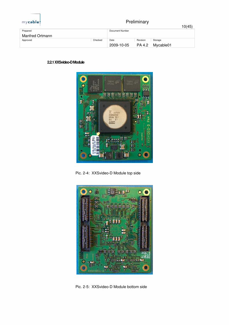
2.2.1 XXSvideoD Module
Pic. 24: XXSvideoD Module top side
Pic. 25: XXSvideoD Module bottom side

Preliminary11(45)
Prepared Document Number
Manfred OrtmannApproved Checked Date Revision Storage
20091005 PA 4.2 Mycable01
2.2.2 XXSvideoD Interface
Pic. 26: XXSvideoD interface
The 120pin 0.5 mm connectors X101 ( CPU signals side ) and X201 ( IO signals side ) QTH06005FDA from Samtec are the interfaces to the XXSvideoD module with the JADED and memory.
Detailed information on the XXSvideoD module see the manual to this board.
Do not plug the XXSvideoD module or EVBJADED when the power supply is on !
Following tables shows the assignment from pins, signals and function of these connectors. Mostly the function is no further elucidated and only the name of the connected pin of the JADED is stated. For further details see the datasheet from the JADED and the schematic of the XXSvideoD module.The signal order is the result of optimisation for a good layout of the XXSvideoD module.

Preliminary12(45)
Prepared Document Number
Manfred OrtmannApproved Checked Date Revision Storage
20091005 PA 4.2 Mycable01
Pin Signal Function
1 VCC33 Power Supply 3.3 V for XXSvideoD
2 VCC33 Power Supply 3.3 V for XXSvideoD
3 MEM_XCS4 Chip Select 4 for Flash Memory
4 VCC33 Power Supply 3.3 V for XXSvideoD
5 CPU_D15 Data
6 VCC33 Power Supply 3.3 V for XXSvideoD
7 CPU_A1 Address
8 GND Ground
9 CPU_A3 Address
10 CPU_D0 Data
11 CPU_A4 Address
12 CPU_D3 Data
13 CPU_A7 Address
14 CPU_D4 Data
15 CPU_A8 Address
16 CPU_D7 Data
17 CPU_A11 Address
18 CPU_D8 Data
19 CPU_A12 Address
20 CPU_D11 Data
21 CPU_A15 Address
22 CPU_D12 Data
23 CPU_A16 Address
24 CPU_D14 Data
25 CPU_A19 Address
26 CPU_D1 Data
27 CPU_A20 Address
28 CPU_D2 Data
29 CPU_A23 Address
30 CPU_D5 Data
31 MEM_XWR1 Write Strobe
32 CPU_D6 Data
33 MEM_XRD Read Strobe
34 CPU_D9 Data
Preliminary13(45)
Prepared Document Number
Manfred OrtmannApproved Checked Date Revision Storage
20091005 PA 4.2 Mycable01
Pin Signal Function
35 MEM_XCS2 Chip Select 2
36 CPU_D10 Data
37 MEM_XCS0 Chip Select 0
38 CPU_D13 Data
39 CPU_A22 Address
40 CPU_A2 Address
41 CPU_A21 Address
42 CPU_A6 Address
43 MEM_XWR0 Write Strobe
44 CPU_A5 Address
45 CPU_A24 Address
46 CPU_A10 Address
47 MEM_RDY Ready input for slow device
48 CPU_A9 Address
49 APIXGND Ground for APIX signals
50 CPU_A14 Address
51 APIX_SDIN2 Serial Data Input 1 ( positive )
52 CPU_A13 Address
53 APIX_SDIN3 Serial Data Input 0 ( negative )
54 CPU_A18 Address
55 APIXGND Ground for APIX signals
56 CPU_A17 Address
57 APIX_SDOUT3 Serial Data Output 1 ( negative )
58 HOST_SPI_DI HOST SPI Data Input ( MOSI )
59 APIX_SDOUT2 Serial Data Output 1 ( positive )
60 HOST_SPI_DO HOST SPI Data Output ( MISO )
61 APIX_SDIN1 Serial Data Input 0 ( negative )
62 HOST_SPI_SS HOST SPI Slave Select
63 APIX_SDIN0 Serial Data Input 0 ( positive )
64 HOST_SPI_SCK HOST SPI Clock
65 APIXGND Ground for APIX signals
66 DCLKIN1 Video output interface 1 dot clock input
67 APIX_SDOUT1 Serial Data Output 0 ( negative )
68 SPI_DI0 SPI0 Master Data Input ( MISO )
69 APIX_SDOUT0 Serial Data Output 0 ( positive )
70 SPI_DO0 SPI0 Master Data Output ( MOSI )

Preliminary14(45)
Prepared Document Number
Manfred OrtmannApproved Checked Date Revision Storage
20091005 PA 4.2 Mycable01
Pin Signal Function
71 APIXGND Ground for APIX signals
72 SPI_SS0 SPI0 Master Slave Select
73 VIN0_7 Video Capture Data Input 0 bit 7
74 SPI_SCK0 SPI0 Master serial clock
75 VIN0_4 Video Capture Data Input 0 bit 4
76 TSG_R_4 TCON Timing Signal
77 VIN0_3 Video Capture Data Input 0 bit 3
78 TSG_R_5 TCON Timing Signal
79 VIN0_5 Video Capture Data Input 0 bit 5
80 TSG_R_6 TCON Timing Signal
81 VIN0_6 Video Capture Data Input 0 bit 6
82 DCLKP RSDS Clock Output CLKp, in TTL Mode
83 VIN0_1 Video Capture Data Input 0 bit 1
84 DCLKN RSDS Clock Output CLKn, in TTL Mode
85 VIN0_2 Video Capture Data Input 0 bit 2
86 DE0 TCON Bypass: DE/CSYNC of DISPL0, TCON:TSG_2
87 VIN0_8 Video Capture 0 Clock
88 HSYNC0 Video Capture 0 Horizontal Syncronisation
89 VIN0_0 Video Capture Data Input 0 bit 0
90 GVO0 Video output interface 0 graphics / video switch
91 TSG_R_7 TCON Timing Signal
92VSYNC0 TCON Bypass: Video output interface 0 vertical sync
output vertical sync input in external sync mode
93 ATST_R APIX analog Test Clock
94 DOUTB1_R_5 Digital RGB output1 with serial resistor
95 PWMO2 PWM Output
96 DOUTB1_R_2 Digital RGB output1 with serial resistor
97 DOUTB1_R_3 Digital RGB output1 with serial resistor
98 DOUTG1_R_3 Digital RGB output1 with serial resistor
99 DOUTB1_R_4 Digital RGB output1 with serial resistor
100 DOUTB1_R_6 Digital RGB output1 with serial resistor
101 DOUTB1_R_7 Digital RGB output1 with serial resistor
102 DOUTG1_R_7 Digital RGB output1 with serial resistor
103 DOUTG1_R_2 Digital RGB output1 with serial resistor
104 DOUTG1_R_4 Digital RGB output1 with serial resistor
105 DOUTG1_R_5 Digital RGB output1 with serial resistor
Preliminary15(45)
Prepared Document Number
Manfred OrtmannApproved Checked Date Revision Storage
20091005 PA 4.2 Mycable01
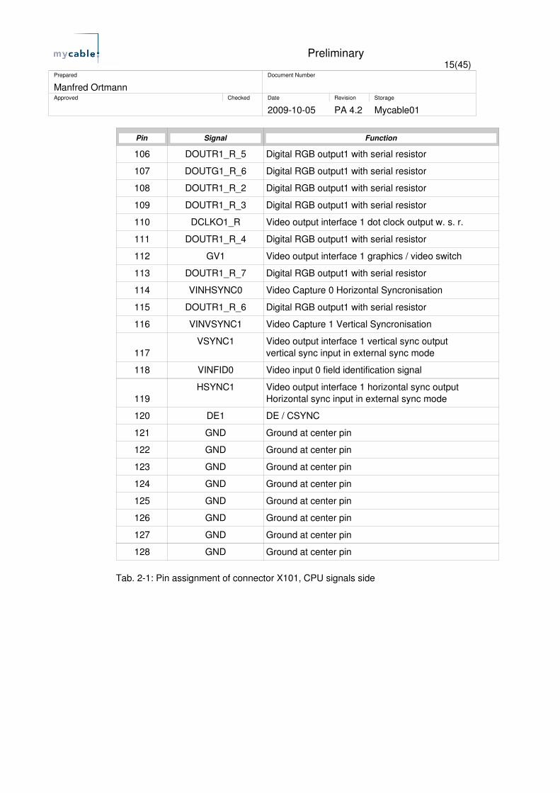
Pin Signal Function
106 DOUTR1_R_5 Digital RGB output1 with serial resistor
107 DOUTG1_R_6 Digital RGB output1 with serial resistor
108 DOUTR1_R_2 Digital RGB output1 with serial resistor
109 DOUTR1_R_3 Digital RGB output1 with serial resistor
110 DCLKO1_R Video output interface 1 dot clock output w. s. r.
111 DOUTR1_R_4 Digital RGB output1 with serial resistor
112 GV1 Video output interface 1 graphics / video switch
113 DOUTR1_R_7 Digital RGB output1 with serial resistor
114 VINHSYNC0 Video Capture 0 Horizontal Syncronisation
115 DOUTR1_R_6 Digital RGB output1 with serial resistor
116 VINVSYNC1 Video Capture 1 Vertical Syncronisation
117VSYNC1 Video output interface 1 vertical sync output
vertical sync input in external sync mode
118 VINFID0 Video input 0 field identification signal
119HSYNC1 Video output interface 1 horizontal sync output
Horizontal sync input in external sync mode
120 DE1 DE / CSYNC
121 GND Ground at center pin
122 GND Ground at center pin
123 GND Ground at center pin
124 GND Ground at center pin
125 GND Ground at center pin
126 GND Ground at center pin
127 GND Ground at center pin
128 GND Ground at center pin
Tab. 21: Pin assignment of connector X101, CPU signals side

Preliminary16(45)
Prepared Document Number
Manfred OrtmannApproved Checked Date Revision Storage
20091005 PA 4.2 Mycable01
Following table shows the assignment from pins, signals and function of connector X201 I/O signals side:
Pin Signal Function
1 VCC33 Power Supply 3.3 V for XXSvideoD
2 VCC33 Power Supply 3.3 V for XXSvideoD
3 VCC33 Power Supply 3.3 V for XXSvideoD
4 VCC33 Power Supply 3.3 V for XXSvideoD
5 GND Ground
6 GND Ground
7 INT_A0 Interrupt 0
8 I2C_SDA0 I2C 0 Data
9 INT_A1 Interrupt 1
10 I2C_SCL0 I2C 0 Clock
11 I2C_SDA1 I2C 1 Data
12 I2C_SCL1 I2C 1 Clock
13 INT_A3 Interrupt 3
14 SPI_DO1 SPI1 Master Data Output ( MOSI )
15 INT_A2 Interrupt 2
16 SPI_DI1 SPI1 Master Data Input ( MISO )
17 TSG_R_10 TCON Timing Signal 10
18 TSG_R_8 TCON Timing Signal 8
19 TSG_R_11 TCON Timing Signal 11
20 TSG_R_9 TCON Timing Signal 9
21 SPI_SCK1 SPI1 Master serial clock
22 UART_SOUT1 UART 1 serial output
23 SPI_SS1 SPI1 Master Slave Select
24 UART_SIN1 UART 1serial input
25 UART_SIN2 UART 2 serial input
26 UART_CTS0# UART 0 Clear to send
27 UART_SOUT2 UART 2 serial output
28 UART_SIN0 UART 0 serial input
29 ADCGND Ground for ADC signals
30 UART_RTS0# UART0 Request to send
31 AD_VRL1 Reference voltage "L" input
32 UART_SOUT0 UART 0 serial output
33 AD_VR1 Reference output

Preliminary17(45)
Prepared Document Number
Manfred OrtmannApproved Checked Date Revision Storage
20091005 PA 4.2 Mycable01
Pin Signal Function
34 ADCGND Ground for ADC signals
35 AD_VRL0 Reference voltage "L" input
36 AD_VRH1 Reference voltage "H" input 1
37 AD_VR0 Reference output
38 AD_VIN1 A/D analog input, channel 1
39 AD_VIN0 A/D analog input, channel 0
40 AD_VRH0 Reference voltage "H" input 0
41 GND Ground
42OPT_PIN_0 A/D analog input, channel 2 or
TESTMODE 2
43DISP_P_R_10 RSDS Output 10p, in TTL Mode
Default=DOUTB0_4
44OPT_PIN_1 A/D analog input, channel 3 or
VINITHI
45DISP_N_R_10 RSDS Output 10n, in TTL Mode
Default=DOUTB0_5
46 VCC12 1.2 V from CPU core voltage regulator
47DISP_P_R_7 RSDS Output 7p, in TTL Mode
Default=DOUTG0_6
48 VCC12 1.2 V from CPU core voltage regulator
49DISP_N_R_7 RSDS Output 7n, in TTL Mode
Default=DOUTG0_7
50DISP_P_R_0 RSDS Output 0p, in TTL Mode
Default=DOUTR0_0
51DISP_P_R_8 RSDS Output 8p, in TTL Mode
Default=DOUTB0_0
52DISP_N_R_0 RSDS Output 0n, in TTL Mode
Default=DOUTR0_1
53DISP_N_R_8 RSDS Output 8n, in TTL Mode
Default=DOUTB0_1
54DISP_P_R_1 RSDS Output 1p, in TTL Mode
Default=DOUTR0_2
55DISP_P_R_9 RSDS Output 9p, in TTL Mode
Default=DOUTB0_2
56DISP_N_R_1 RSDS Output 1n, in TTL Mode
Default=DOUTR0_3
57DISP_N_R_9 RSDS Output 9n, in TTL Mode
Default=DOUTB0_3
58DISP_P_R_2 RSDS Output 2p, in TTL Mode
Default=DOUTR0_4
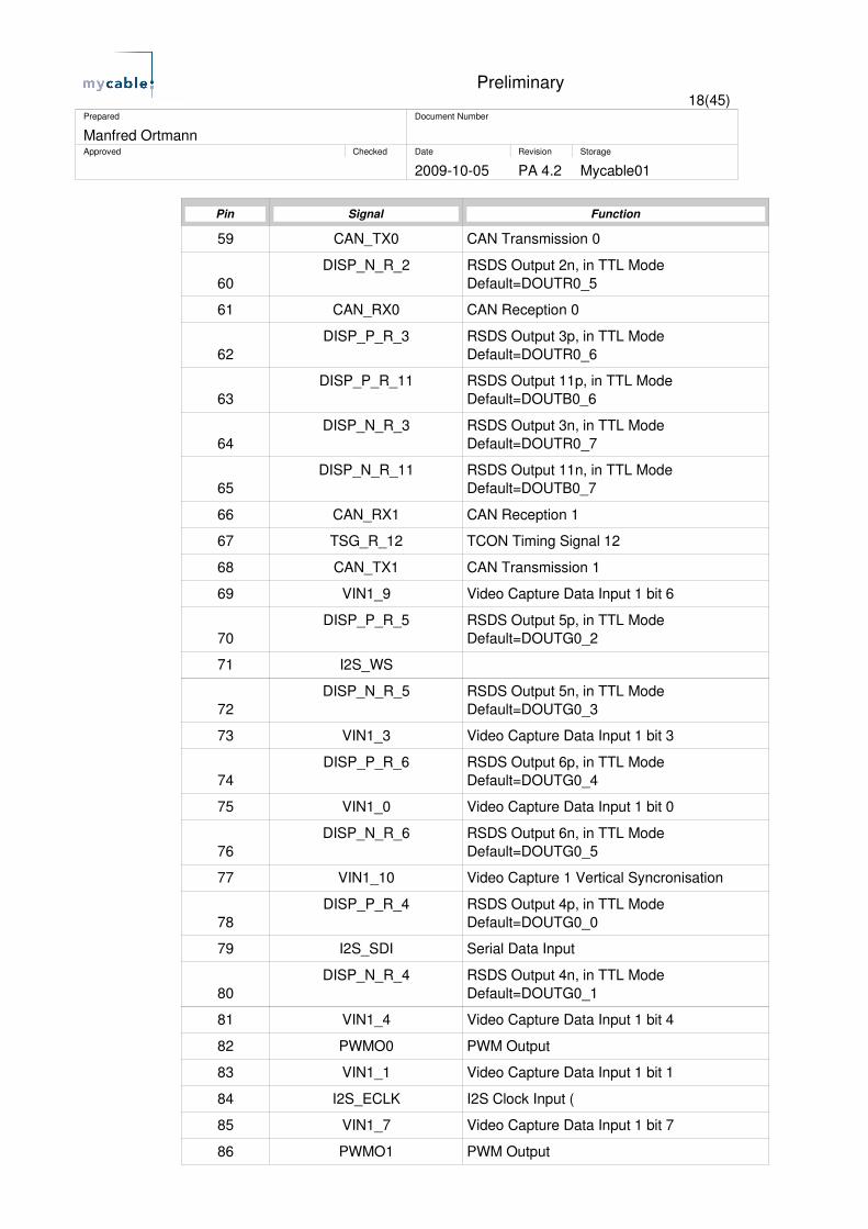
Preliminary18(45)
Prepared Document Number
Manfred OrtmannApproved Checked Date Revision Storage
20091005 PA 4.2 Mycable01
Pin Signal Function
59 CAN_TX0 CAN Transmission 0
60DISP_N_R_2 RSDS Output 2n, in TTL Mode
Default=DOUTR0_5
61 CAN_RX0 CAN Reception 0
62DISP_P_R_3 RSDS Output 3p, in TTL Mode
Default=DOUTR0_6
63DISP_P_R_11 RSDS Output 11p, in TTL Mode
Default=DOUTB0_6
64DISP_N_R_3 RSDS Output 3n, in TTL Mode
Default=DOUTR0_7
65DISP_N_R_11 RSDS Output 11n, in TTL Mode
Default=DOUTB0_7
66 CAN_RX1 CAN Reception 1
67 TSG_R_12 TCON Timing Signal 12
68 CAN_TX1 CAN Transmission 1
69 VIN1_9 Video Capture Data Input 1 bit 6
70DISP_P_R_5 RSDS Output 5p, in TTL Mode
Default=DOUTG0_2
71 I2S_WS
72DISP_N_R_5 RSDS Output 5n, in TTL Mode
Default=DOUTG0_3
73 VIN1_3 Video Capture Data Input 1 bit 3
74DISP_P_R_6 RSDS Output 6p, in TTL Mode
Default=DOUTG0_4
75 VIN1_0 Video Capture Data Input 1 bit 0
76DISP_N_R_6 RSDS Output 6n, in TTL Mode
Default=DOUTG0_5
77 VIN1_10 Video Capture 1 Vertical Syncronisation
78DISP_P_R_4 RSDS Output 4p, in TTL Mode
Default=DOUTG0_0
79 I2S_SDI Serial Data Input
80DISP_N_R_4 RSDS Output 4n, in TTL Mode
Default=DOUTG0_1
81 VIN1_4 Video Capture Data Input 1 bit 4
82 PWMO0 PWM Output
83 VIN1_1 Video Capture Data Input 1 bit 1
84 I2S_ECLK I2S Clock Input (
85 VIN1_7 Video Capture Data Input 1 bit 7
86 PWMO1 PWM Output

Preliminary19(45)
Prepared Document Number
Manfred OrtmannApproved Checked Date Revision Storage
20091005 PA 4.2 Mycable01
Pin Signal Function
87 VIN1_5 Video Capture Data Input 1 bit 5
88 I2S_SCK I2S Clock Output
89 VIN1_6 Video Capture Data Input 1 bit 6
90 I2S_SDO Serial Data Output
91 MLB_SIG Media LB Control Pin
92 CCLK1 Video Capture 1 Clock
93 MLB_CLK Media LB Clock Pin
94 VIN1_2 Video Capture Data Input 1 bit 2
95 MLB_DAT Media LB Data Pin
96 MPX_MODE_1_0 Multiplex Mode Pin
97 RTCK Return test clock
98 MPX_MODE_1_1 Multiplex Mode Pin
99 TCK JTAG Test Clock
100 VINFID1 Video input 1 field identification signal
101 TMS JTAG TMS
102JTAGSEL JTAG Selector ( 0 = Fujitsu TAP Controller, 1
= ARM Tap Controller )
103 TDO JTAG TDO
104 XSRST ICE System reset
105TRACEDATA_0 Trace data used by the trace tool such as
RealView supplied by ARM Limited.
106 XTRST Test reset
107TRACEDATA_2 Trace data used by the trace tool such as
RealView supplied by ARM Limited.
108 TDI JTAG TDI
109 TRACECTL TRACE control
110 VCC_CORE_PG Power good CPU core voltage
111TRACEDATA_1 Trace data used by the trace tool such as
RealView supplied by ARM Limited.
112 MR# Master reset input
113 GND Ground
114 RESET# Reset output
115 GND Ground
116 WDI Watch dog input
117TRACEDATA_3 Trace data used by the trace tool such as
RealView supplied by ARM Limited.

Preliminary20(45)
Prepared Document Number
Manfred OrtmannApproved Checked Date Revision Storage
20091005 PA 4.2 Mycable01
Pin Signal Function
118VCC18 1.8 V, regulated on XXSvideoD for DDR2
SDRAM
119 TRACECLK Trace clock
120VCC18 1.8 V, regulated on XXSvideoD for DDR2
SDRAM
121 GND Ground at center pin
122 GND Ground at center pin
123 GND Ground at center pin
124 GND Ground at center pin
125 GND Ground at center pin
126 GND Ground at center pin
127 GND Ground at center pin
128 GND Ground at center pin
Tab. 22: Pin assignment of connector X201, I/O signals side

Preliminary21(45)
Prepared Document Number
Manfred OrtmannApproved Checked Date Revision Storage
20091005 PA 4.2 Mycable01
2.2.3 XXSvideo Interface
Pic. 27: XXSvideo interface
The connectors X301 ( CPU signals side ) and X401 ( I/O signals side ) DF17(3.0)120DS0.5V(51) from Hirose are the interfaces to the JADE Evaluation board.
These interfaces are specified for the XXSvideo module with the JADE Evaluation board.
Mostly the function is no further elucidated and only the name of the connected pin of the JADE is stated. For further details see the datasheet from the JADE and the schematic of the XXSvideo module.Signals with the name JADE_IO_Gn are connected to multi function pins of the JADE.N indicate the function group.
Following table shows the assignment from pins, signals and function of connector X301 CPU signals side:

Preliminary22(45)
Prepared Document Number
Manfred OrtmannApproved Checked Date Revision Storage
20091005 PA 4.2 Mycable01
Pin Signal Function
1 VCC33 Power Supply 3.3 V for XXSvideo
2 VCC33 Power Supply 3.3 V for XXSvideo
3 VCC33 Power Supply 3.3 V for XXSvideo
4 VCC33 Power Supply 3.3 V for XXSvideo
5 GND Ground
6 GND Ground
7 GND Ground
8 GND Ground
9 CPU_D15 Data
10 CPU_D0 Data
11 CPU_A1 Address
12 CPU_D3 Data
13 CPU_A3 Address
14 CPU_D4 Data
15 CPU_A4 Address
16 CPU_D7 Data
17 CPU_A7 Address
18 CPU_D8 Data
19 CPU_A8 Address
20 CPU_D11 Data
21 CPU_A11 Address
22 CPU_D12 Data
23 CPU_A12 Address
24 CPU_D14 Data
25 CPU_A15 Address
26 CPU_D1 Data
27 CPU_A16 Address
28 CPU_D2 Data
29 CPU_A19 Address
30 CPU_D5 Data
31 CPU_A20 Address
32 CPU_D6 Data
33 CPU_A23 Address
Preliminary23(45)
Prepared Document Number
Manfred OrtmannApproved Checked Date Revision Storage
20091005 PA 4.2 Mycable01
Pin Signal Function
34 CPU_D9 Data
35 MEM_XWR1 Write Strobe
36 CPU_D10 Data
37 MEM_XRD Read Strobe
38 CPU_D13 Data
39 MEM_CS2 Chip Select 2
40 CPU_A2 Address
41 MEM_CS0 Chip Select 0
42 CPU_A6 Address
43 CPU_A22 Address
44 CPU_A5 Address
45 CPU_A21 Address
46 CPU_A10 Address
47 MEM_XWR0 Write Strobe
48 CPU_A9 Address
49 CPU_A24 Address
50 CPU_A14 Address
51 MEM_RDY Ready input for slow device
52 CPU_A13 Address
53 JADE_VO0_23 Digital RGB output 0 Data B7
54 CPU_A18 Address
55 JADE_VO0_22 Digital RGB output 0 Data B6
56 CPU_A17 Address
57 JADE_VO0_18 Digital RGB output 0 Data B2
58 JADE_IO_G4_28 IDE_DD_3 / GPIO_PD_15
59 JADE_VO0_19 Digital RGB output 0 Data B3
60 JADE_IO_G4_29 IDE_DD_2 / GPIO_PD_14
61 JADE_VO0_14 Digital RGB output 0 Data G4
62 JADE_IO_G4_30 IDE_DD_1 / GPIO_PD_13
63 JADE_VO0_15 Digital RGB output 0 Data G5
64 JADE_IO_G4_31 IDE_DD_0 /
65 VIN0_7 Video Capture Data
66 JADE_IO_G1_0 DCLKIN1
67 VIN0_4 Video Capture Data
68 JADE_VO0_21 Digital RGB output 0 Data B5
69 VIN0_3 Video Capture Data
Preliminary24(45)
Prepared Document Number
Manfred OrtmannApproved Checked Date Revision Storage
20091005 PA 4.2 Mycable01
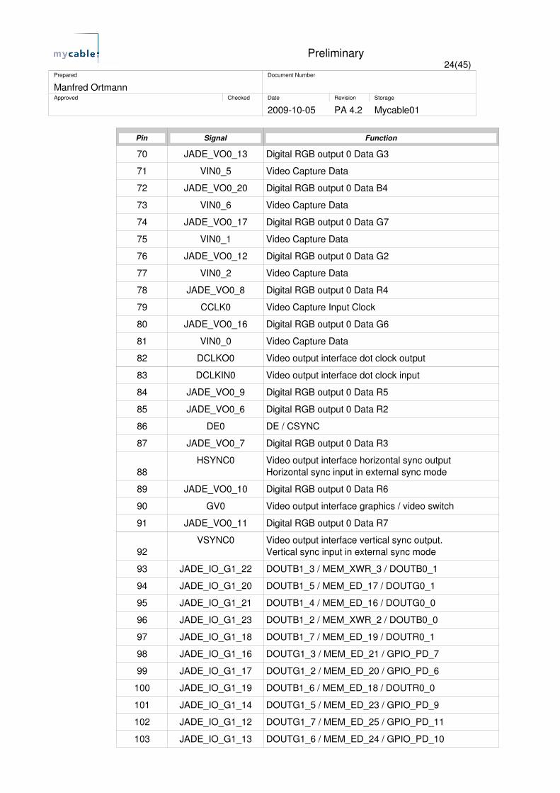
Pin Signal Function
70 JADE_VO0_13 Digital RGB output 0 Data G3
71 VIN0_5 Video Capture Data
72 JADE_VO0_20 Digital RGB output 0 Data B4
73 VIN0_6 Video Capture Data
74 JADE_VO0_17 Digital RGB output 0 Data G7
75 VIN0_1 Video Capture Data
76 JADE_VO0_12 Digital RGB output 0 Data G2
77 VIN0_2 Video Capture Data
78 JADE_VO0_8 Digital RGB output 0 Data R4
79 CCLK0 Video Capture Input Clock
80 JADE_VO0_16 Digital RGB output 0 Data G6
81 VIN0_0 Video Capture Data
82 DCLKO0 Video output interface dot clock output
83 DCLKIN0 Video output interface dot clock input
84 JADE_VO0_9 Digital RGB output 0 Data R5
85 JADE_VO0_6 Digital RGB output 0 Data R2
86 DE0 DE / CSYNC
87 JADE_VO0_7 Digital RGB output 0 Data R3
88HSYNC0 Video output interface horizontal sync output
Horizontal sync input in external sync mode
89 JADE_VO0_10 Digital RGB output 0 Data R6
90 GV0 Video output interface graphics / video switch
91 JADE_VO0_11 Digital RGB output 0 Data R7
92VSYNC0 Video output interface vertical sync output.
Vertical sync input in external sync mode
93 JADE_IO_G1_22 DOUTB1_3 / MEM_XWR_3 / DOUTB0_1
94 JADE_IO_G1_20 DOUTB1_5 / MEM_ED_17 / DOUTG0_1
95 JADE_IO_G1_21 DOUTB1_4 / MEM_ED_16 / DOUTG0_0
96 JADE_IO_G1_23 DOUTB1_2 / MEM_XWR_2 / DOUTB0_0
97 JADE_IO_G1_18 DOUTB1_7 / MEM_ED_19 / DOUTR0_1
98 JADE_IO_G1_16 DOUTG1_3 / MEM_ED_21 / GPIO_PD_7
99 JADE_IO_G1_17 DOUTG1_2 / MEM_ED_20 / GPIO_PD_6
100 JADE_IO_G1_19 DOUTB1_6 / MEM_ED_18 / DOUTR0_0
101 JADE_IO_G1_14 DOUTG1_5 / MEM_ED_23 / GPIO_PD_9
102 JADE_IO_G1_12 DOUTG1_7 / MEM_ED_25 / GPIO_PD_11
103 JADE_IO_G1_13 DOUTG1_6 / MEM_ED_24 / GPIO_PD_10

Preliminary25(45)
Prepared Document Number
Manfred OrtmannApproved Checked Date Revision Storage
20091005 PA 4.2 Mycable01
Pin Signal Function
104 JADE_IO_G1_15 DOUTG1_4 / MEM_ED_22 / GPIO_PD_8
105 JADE_IO_G1_10 DOUTR1_3 / MEM_ED_27 / I2S_SDO0
106 JADE_IO_G1_8 DOUTR1_5 / MEM_ED_29 / I2S_WS0
107 JADE_IO_G1_9 DOUTR1_4 / MEM_ED_28 / I2S_SDI0
108 JADE_IO_G1_11 DOUTR1_2 / MEM_ED_26 / GPIO_PD_12
109 JADE_IO_G1_6 DOUTR1_7 / MEM_ED_31 / I2S_ECLK0
110 JADE_IO_G1_1 DCLKO1
111 JADE_IO_G1_7 DOUTR1_6 / MEM_ED_30 / I2S_SCK0
112 JADE_IO_G1_5 GV1 / DREQ_7 / DREQ_7
113 JADE_IO_G1_4 VSYNC1 / XDACK_6 / XDACK_6
114 USB_PWR_CTRL USB Port Power Control
115 JADE_IO_G1_3 HSYNC1 / DREQ_6 / DREQ_6
116 USB_DP D+ for HS and FS
117 JADE_IO_G1_2 DE1 / XDACK_7 / XDACK_7
118 USB_DM D for HS and FS
119 GND Ground
120 GND Ground
Tab. 23: Pin assignment of connector X301, CPU signals side

Preliminary26(45)
Prepared Document Number
Manfred OrtmannApproved Checked Date Revision Storage
20091005 PA 4.2 Mycable01
Following table shows the assignment from pins, signals and function of connector X401 I/O signals side:
Pin Signal Function
1 VCC33 Power Supply 3.3 V for XXSvideo
2 VCC33 Power Supply 3.3 V for XXSvideo
3 VCC33 Power Supply 3.3 V for XXSvideo
4 VCC33 Power Supply 3.3 V for XXSvideo
5 GND Ground
6 GND Ground
7 GND Ground
8 GND Ground
9 INT_A0 INT_A0
10 I2C1 I2C_SDA0
11 INT_A1 INT_A1
12 I2C0 I2C_SCL0
13 I2C3 I2C_SDA1
14 I2C2 I2C_SCL1
15 INT_A3 INT_A3
16 SD_CARD7 SD_XMCD
17 INT_A2 INT_A2
18 SD_CARD6 SD_WP
19 SD_CARD5 SD_DAT3
20 SD_CARD3 SD_DAT1
21 SD_CARD4 SD_DAT2
22 SD_CARD2 SD_DAT0
23 SD_CARD0 SD_CLK
24 UART5 UART_SOUT1
25 SD_CARD1 SD_CMD
26 UART4 UART_SIN1
27 UART6 UART_SIN2
28 UART2 UART_CTS0#
29 UART7 UART_SOUT2
30 UART0 UART_SIN0
31 ADC5 AD_VRL1
32 UART3 UART_RTS0#
33 ADC7 AD_VR1

Preliminary27(45)
Prepared Document Number
Manfred OrtmannApproved Checked Date Revision Storage
20091005 PA 4.2 Mycable01
Pin Signal Function
34 UART1 UART_SOUT0
35 ADC1 AD_VRL0
36 ADC4 AD_VRH1
37 ADC3 AD_VR0
38 ADC6 AD_VIN1
39 ADC2 AD_VIN0
40 ADC0 AD_VRH0
41 JADE_IO_G4_13 IDE_XDIOW /
42 BIGEND BIGEND
43 JADE_IO_G4_12 IDE_XDIOR /
44 VINITHI VINITHI
45 GND Ground
46VCC12 1.2 V JADE core voltage, regulated on
XXSvideo
47 JADE_IO_G4_7 IDE_DA_2 /
48VCC12 1.2 V JADE core voltage, regulated on
XXSvideo
49 JADE_IO_G4_8 IDE_DA_1 / PWMO1
50 JADE_IO_G4_10 IDE_XDCS_1 /
51 JADE_IO_G4_24 IDE_DD_7 / GPIO_PD_19
52 JADE_IO_G4_11 IDE_XDCS_0 /
53 JADE_IO_G4_25 IDE_DD_6 / GPIO_PD_18
54 JADE_IO_G4_14 IDE_CSEL /
55 JADE_IO_G4_20 IDE_DD_11 / GPIO_PD_23
56 JADE_IO_G4_9 IDE_DA_0 / PWMO0
57 JADE_IO_G4_21 IDE_DD_10 / GPIO_PD_22
58 JADE_IO_G4_27 IDE_DD_4 / GPIO_PD_16
59 JADE_IO_G4_16 IDE_DD_15 / CAN_TX0
60 JADE_IO_G4_26 IDE_DD_5 / GPIO_PD_17
61 JADE_IO_G4_17 IDE_DD_14 / CAN_RX0
62 JADE_IO_G4_23 IDE_DD_8 / GPIO_PD_20
63 JADE_IO_G4_4 IDE_DINTRQ / I2S_SDO1
64 JADE_IO_G4_22 IDE_DD_9 / GPIO_PD_21
65 JADE_IO_G4_3 IDE_DDMARQ/ I2S_ECLK1
66 JADE_IO_G4_19 IDE_DD_12 / CAN_RX1
67 JADE_IO_G4_6 IDE_DIORDY /

Preliminary28(45)
Prepared Document Number
Manfred OrtmannApproved Checked Date Revision Storage
20091005 PA 4.2 Mycable01
Pin Signal Function
68 JADE_IO_G4_18 IDE_DD_13 / CAN_TX1
69JADE_IO_G2_5 VINHSYNC1 / VINHSYNC1 / I2S_SDI1 /
I2S_SDI1 / I2S_SDI1
70 JADE_IO_G4_15 IDE_XDDMACK /
71JADE_IO_G2_20 I2SWS0 / BI1_3 / I2S_WS2 / SPI_SS /
I2S_WS2
72 JADE_IO_G4_0 IDE_XDRESET /
73JADE_IO_G2_11 VIN1_3 / RI1_3 / CAN_TX1 / CAN_TX1 /
CAN_TX1
74 JADE_IO_G4_2 IDE_XDASP / I2S_WS1
75JADE_IO_G2_14 VIN1_0 / GI1_6 / I2S_WS1 / I2S_WS1 /
I2S_WS1
76 JADE_IO_G4_1 IDE_XIOCS16 / I2S_SDI1
77JADE_IO_G2_4 VINVSYNC1 / VINVSYNC1 / I2S_ECLK1 /
I2S_ECLK1 / I2S_ECLK1
78 JADE_IO_G4_5 IDE_XCBLID / I2S_SCK1
79JADE_IO_G2_21 I2S_SDI0 / BI1_2 / I2S_SDI2 / SPI_DI /
I2S_SDI2
80JADE_IO_G2_15 PWMO0 / GI1_2 / GPIO_PD_3 /
GPIO_PD_3 / GPIO_PD_3
81JADE_IO_G2_10 VIN1_4 / RI1_4 / CAN_RX0 / CAN_RX0 /
CAN_RX0
82JADE_IO_G2_18 I2S_ECLK0 / BI1_5 / I2S_ECLK2 / reserved /
GPIO_PD_0
83JADE_IO_G2_13 VIN1_1 / GI1_7 / I2S_SCK1 / I2S_SCK1 /
I2S_SCK1
84JADE_IO_G2_16 PWMO1 / BI1_7 / GPIO_PD_2 /
GPIO_PD_2 / GPIO_PD_2
85JADE_IO_G2_7 VIN1_7 / RI1_7 / GPIO_PD_5 / GPIO_PD_5 /
GPIO_PD_5
86JADE_IO_G2_19 I2S_SCK0 / BI1_4 / I2S_SCK2 / SPI_SCK /
I2S_SCK2
87JADE_IO_G2_9 VIN1_5 / RI1_5 / CAN_TX0 / CAN_TX0 /
CAN_TX0
88JADE_IO_G2_17 I2S_SDO0 / BI1_6 / I2S_SDO2 / SPI_DO /
GPIO_PD_1
89JADE_IO_G2_8 VIN1_6 / RI1_6 / GPIO_PD_4 / GPIO_PD_4 /
GPIO_PD_4
90JADE_IO_G2_6 VINFID1 / VINFID1 / I2S_SDO1 / I2S_SDO1 /
I2S_SDO1
Preliminary29(45)
Prepared Document Number
Manfred OrtmannApproved Checked Date Revision Storage
20091005 PA 4.2 Mycable01
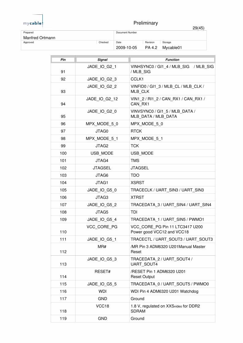
Pin Signal Function
91JADE_IO_G2_1 VINHSYNC0 / GI1_4 / MLB_SIG / MLB_SIG
/ MLB_SIG
92 JADE_IO_G2_3 CCLK1
93JADE_IO_G2_2 VINFID0 / GI1_3 / MLB_CL / MLB_CLK /
MLB_CLK
94JADE_IO_G2_12 VIN1_2 / RI1_2 / CAN_RX1 / CAN_RX1 /
CAN_RX1
95JADE_IO_G2_0 VINVSYNC0 / GI1_5 / MLB_DATA /
MLB_DATA / MLB_DATA
96 MPX_MODE_5_0 MPX_MODE_5_0
97 JTAG0 RTCK
98 MPX_MODE_5_1 MPX_MODE_5_1
99 JTAG2 TCK
100 USB_MODE USB_MODE
101 JTAG4 TMS
102 JTAGSEL JTAGSEL
103 JTAG6 TDO
104 JTAG1 XSRST
105 JADE_IO_G5_0 TRACECLK / UART_SIN3 / UART_SIN3
106 JTAG3 XTRST
107 JADE_IO_G5_2 TRACEDATA_3 / UART_SIN4 / UART_SIN4
108 JTAG5 TDI
109 JADE_IO_G5_4 TRACEDATA_1 / UART_SIN5 / PWMO1
110VCC_CORE_PG VCC_CORE_PG Pin 11 LTC3417 U200
Power good VCC12 and VCC18
111 JADE_IO_G5_1 TRACECTL / UART_SOUT3 / UART_SOUT3
112MR# /MR Pin 3 ADM6320 U201Manual Master
Reset
113JADE_IO_G5_3 TRACEDATA_2 / UART_SOUT4 /
UART_SOUT4
114RESET# /RESET Pin 1 ADM6320 U201
Reset Output
115 JADE_IO_G5_5 TRACEDATA_0 / UART_SOUT5 / PWMO0
116 WDI WDI Pin 4 ADM6320 U201 Watchdog
117 GND Ground
118VCC18 1.8 V, regulated on XXSvideo for DDR2
SDRAM
119 GND Ground
Preliminary30(45)
Prepared Document Number
Manfred OrtmannApproved Checked Date Revision Storage
20091005 PA 4.2 Mycable01
Pin Signal Function
120VCC18 1.8 V, regulated on XXSvideo for DDR2
SDRAM
Tab. 24: Pin assignment of connector X401, I/O signals side
2.2.4 Configuration
R201 R204
R301 R306
R401 – R408
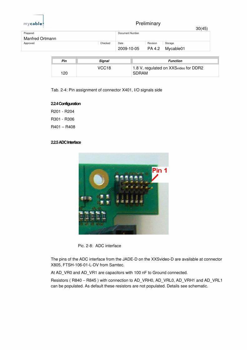
2.2.5 ADC Interface
Pic. 28: ADC interface
The pins of the ADC interface from the JADED on the XXSvideoD are available at connector X805, FTSH10601LDV from Samtec.
At AD_VR0 and AD_VR1 are capacitors with 100 nF to Ground connected.
Resistors ( R840 – R845 ) with connection to AD_VRH0, AD_VRL0, AD_VRH1 and AD_VRL1 can be populated. As default these resistors are not populated. Details see schematic.

Preliminary31(45)
Prepared Document Number
Manfred OrtmannApproved Checked Date Revision Storage
20091005 PA 4.2 Mycable01
Following table shows the assignment of pins, signals and function from the connector X805.
Pin Signal Function
1 AD_VRH0
2 AD_VRL0
3 AD_VIN0
4 AD_VR0
5 AD_VRH1
6 AD_VRL1
7 AD_VIN1
8 AD_VINR1
9 AD_VIN2
10 AD_VIN3
11 ADCGND ADC Ground
12 ADCGND ADC Ground
Tab. 25: Pin assignment of connector X805

Preliminary32(45)
Prepared Document Number
Manfred OrtmannApproved Checked Date Revision Storage
20091005 PA 4.2 Mycable01
2.2.5 I2C and Host SPI Interface
Pic. 29: I2C and Host SPI interface, X806
The pins of the I2C 1and Host SPI interface from the JADED on the XXSvideoD are available at connector X806, FTSH10601LDV from Samtec.
Following table shows the assignment of pins, signals and function from the connector X806.
Pin Signal Function
1 Not connected
2 I2C_SDA1 SDA from I2C interface 1
3 I2C_SCL1 SCL from I2C interface 1
4 GND Ground
5 HOST_SPI_SCK
6 GND Ground
7 HOST_SPI_DI
8 GND Ground
9 HOST_SPI_DO
10 GND Ground
11 HOST_SPI_SS
12 VCC33 + 3.3 V output
Tab. 26: Pin assignment of connector X805
Preliminary33(45)
Prepared Document Number
Manfred OrtmannApproved Checked Date Revision Storage
20091005 PA 4.2 Mycable01
2.2.6 32 bit Flash Memory
For evaluation reasons two 256 MBit MirrorBit Flash memories ( S29GL256N10FFI02 from Spansion, U503 and U504 ) which can be configured for the 32 bit bus of the JADED are available on the EVB JADED Interface board.
The 32bit mode can be configured by setting the MPX_MODE_1 [1:0] pins b'10'.
See config switch SW901 on JADE Evaluation board.
2.2.7 USB
A USB 2.0 highspeed mode host and device controller LSI with 16bit width standard CPU bus S1R72V18 ( U601 ) from Seiko Epson Corporation is populated. The S1R72V18 has two host ports to function as a USB root hub. One of the ports can be used as a USB device port after setting.
On the EVB JADED Interface board only the host port will be used.
The interrupt output from the USB controller is connected to the JADED interrupt A1 over 0 Ohm resistor R605, A2 over 0 Ohm resistor R606 and A3 over 0 Ohm resistor R607. Remove the corresponding resistor to disconnect the connection which shall not be used !
Preliminary34(45)
Prepared Document Number
Manfred OrtmannApproved Checked Date Revision Storage
20091005 PA 4.2 Mycable01
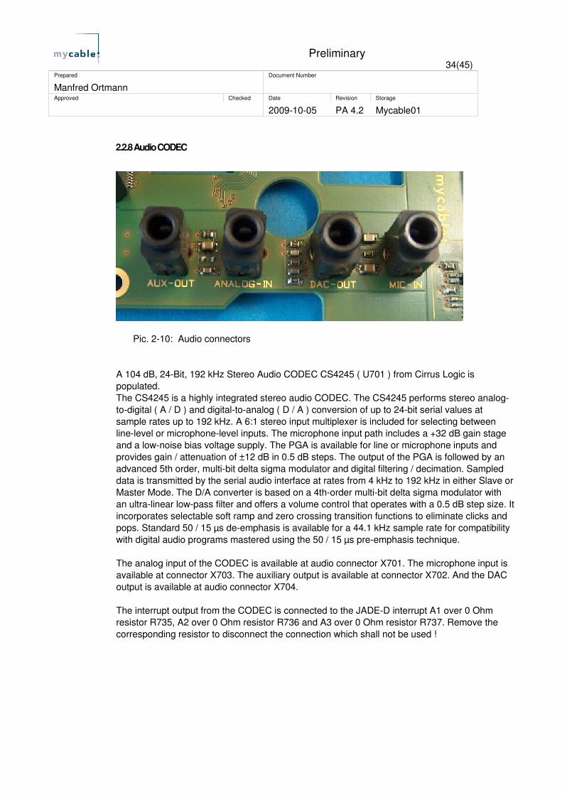
2.2.8 Audio CODEC
Pic. 210: Audio connectors
A 104 dB, 24Bit, 192 kHz Stereo Audio CODEC CS4245 ( U701 ) from Cirrus Logic is populated.The CS4245 is a highly integrated stereo audio CODEC. The CS4245 performs stereo analogtodigital ( A / D ) and digitaltoanalog ( D / A ) conversion of up to 24bit serial values at sample rates up to 192 kHz. A 6:1 stereo input multiplexer is included for selecting between linelevel or microphonelevel inputs. The microphone input path includes a +32 dB gain stage and a lownoise bias voltage supply. The PGA is available for line or microphone inputs and provides gain / attenuation of ±12 dB in 0.5 dB steps. The output of the PGA is followed by an advanced 5th order, multibit delta sigma modulator and digital filtering / decimation. Sampled data is transmitted by the serial audio interface at rates from 4 kHz to 192 kHz in either Slave or Master Mode. The D/A converter is based on a 4thorder multibit delta sigma modulator with an ultralinear lowpass filter and offers a volume control that operates with a 0.5 dB step size. It incorporates selectable soft ramp and zero crossing transition functions to eliminate clicks and pops. Standard 50 / 15 μs deemphasis is available for a 44.1 kHz sample rate for compatibility with digital audio programs mastered using the 50 / 15 μs preemphasis technique.
The analog input of the CODEC is available at audio connector X701. The microphone input is available at connector X703. The auxiliary output is available at connector X702. And the DAC output is available at audio connector X704.
The interrupt output from the CODEC is connected to the JADED interrupt A1 over 0 Ohm resistor R735, A2 over 0 Ohm resistor R736 and A3 over 0 Ohm resistor R737. Remove the corresponding resistor to disconnect the connection which shall not be used !

Preliminary35(45)
Prepared Document Number
Manfred OrtmannApproved Checked Date Revision Storage
20091005 PA 4.2 Mycable01
2.2.9 APIX
Pic. 211: APIX connectors
APIX is a serial Gbit/s link for incar infotainment and driver assistance systems. It features unidirectional pixel and fullduplex sideband data transmission over one single pair of a shielded twisted pair ( STP ) copper cable. The downlink channel provides a sustained data rate of up to 1 Gbit / s, another 18 Mbit / s can be transmitted simultaneously in uplink direction.
The APIX interface 0 from the JADED is connected to connector X801 with pinning for input side.
The APIX interface 1 from the JADED is connected to connector X802 with pinning for output side.
On revision PA3 both connectors have input pinning.
The lines have no external ESD protection diodes because the 1.2 V APIX power supply is not available on this board. The internal protection of the JADED is for up to 2 kV.

Preliminary36(45)
Prepared Document Number
Manfred OrtmannApproved Checked Date Revision Storage
20091005 PA 4.2 Mycable01
Following tables shows the assignment of pins, signals and function from the APIX connectors.
Pin Signal Function
1 SDIN0_P CML serial data interface downstream. Interface to differential transmission line
2 SDIN0_M CML serial data interface downstream. Interface to differential transmission line
3 NC Not connected
4 SDOUT0_P CML serial data interface upstream. Interface to differential transmission line
5 SDOUT0_M CML serial data interface upstream. Interface to differential transmission line
6 NC Not connected
7 NC Not connected
8 NC Not connected
Tab. 27: Pin assignment of input connector X801
Pin Signal Function
1 SDOUT1_P CML serial data interface upstream. Interface to differential transmission line
2 SDOUT1_M CML serial data interface upstream. Interface to differential transmission line
3 NC Not connected
4 SDIN1_P CML serial data interface downstream. Interface to differential transmission line
5 SDIN1_M CML serial data interface downstream. Interface to differential transmission line
6 NC Not connected
7 NC Not connected
8 NC Not connected
Tab. 28: Pin assignment of output connector X802

Preliminary37(45)
Prepared Document Number
Manfred OrtmannApproved Checked Date Revision Storage
20091005 PA 4.2 Mycable01
2.2.10 Video Output
Pic. 212: Video output connector, X804
The video output 0 signals from the JADED are connected to connector X804, FTSH12501LDV from Samtec, for direct interconnect to column and row drivers via LVTTL or RSDS from a display.Additional these signals are connected to the JADE Evaluation board connector X301 over 0 Ohm resistors. So the RGB interface 0 on the JADE Evaluation board can be used.If the TCON interface will be used and the long connection to the JADE Evaluation board make disruptions remove the 0 Ohm resistors.On revision PA3 the pin 3 to 14 have another order.
Pin Signal Function
1 GND Ground
2 NC Testpoint 801
3 DISP_N_R_11 DOUTB0_7
4 DISP_P_R_11 DOUTB0_6
5 DISP_N_R_10 DOUTB0_5
6 DISP_P_R_10 DOUTB0_4
7 DISP_N_R_9 DOUTB0_3
8 DISP_P_R_9 DOUTB0_2
9 DISP_N_R_7 DOUTG0_7
10 DISP_P_R_7 DOUTG0_6
11 DISP_N_R_5 DOUTG0_5

Preliminary38(45)
Prepared Document Number
Manfred OrtmannApproved Checked Date Revision Storage
20091005 PA 4.2 Mycable01
Pin Signal Function
12 DISP_P_R_6 DOUTG0_4
13 DISP_N_R_5 DOUTG0_3
14 DISP_P_R_5 DOUTG0_2
15 GND
16 DISP_SYNC_R_3 DCLKP
17 DISP_SYNC_R_4 DCLKN
18 NC Testpoint 802
19 NC Testpoint 800
20 DISP_P_R_3 DOUTR0_6
21 DISP_N_R_3
22 DISP_P_R_2 DOUTR0_4
23 DISP_N_R_2
24 DISP_P_R_1 DOUTR0_2
25 DISP_N_R_1
26 DISP_P_R_8
27 DISP_N_R_8
28 DISP_P_R_4
29 DISP_N_R_4
30 DISP_P_R_0
31 DISP_N_R_0
32 TSG_R_4
33 TSG_R_5
34 TSG_R_6
35 TSG_R_7
36 TSG_R_8
37 TSG_R_9
38 TSG_R_10
39 TSG_R_11
40 GND
41 TSG_R_12

Preliminary39(45)
Prepared Document Number
Manfred OrtmannApproved Checked Date Revision Storage
20091005 PA 4.2 Mycable01
Pin Signal Function
42 GND
43 DISP_SYNC_R_0 HSYNC0
44 DISP_SYNC_R_1 VSYNC0
45 DISP_SYNC_R_2 GVO0
46 Testpoint 803
47 GND Ground
48 Testpoint 804
49 DISP_SYNC_R_5 DE0
50 VCC33 + 3.3 V output voltage
Tab. 29: Pin assignment of connector X804

Preliminary40(45)
Prepared Document Number
Manfred OrtmannApproved Checked Date Revision Storage
20091005 PA 4.2 Mycable01
2.2.11 RGB Input
Pic. 213: RGB input, X900
X900 ( CT0915P5K27, HDDSUBConnector from Yamaichi ) is the connector for the RGB graphic signal which will be captured from the AD9883A from Analog Devices ( U900 ) on the EVB JADED Interface board.
The AD9883A is a complete 8bit, 140 MSPS, monolithic analog interface optimized for capturing RGB graphics signals. Its 140 MSPS encode rate capability and full power analog bandwidth of 300 MHz supports resolutions up to SXGA ( 1280 × 1024 at 75 Hz ). The AD9883A includes a 140 MHz triple ADC with internal 1.25 V reference, a PLL, and programmable gain, offset, and clamp control. This interface is fully programmable via a 2wire serial interface.
Following table shows the assignment of pins, signals and function from the RGB Input connector.

Preliminary41(45)
Prepared Document Number
Manfred OrtmannApproved Checked Date Revision Storage
20091005 PA 4.2 Mycable01
Pin Signal Description
1 AVIN2_RED Analog Red Signal
2 AVIN2_GREEN Analog Green Signal
3 AVIN2_BLUE Analog Blue Signal
4 NC Not connected
5 GND Ground
6 GND Ground
7 GND Ground
8 GND Ground
9 NC Not connected
10 GND Ground
11 NC Not connected
12 NC Not connected
13 AVIN2_HSYNC Horizontal Sync Signal
14 AVIN2_VSYNC Vertical Sync Signal
15 NC Not connected
Tab. 210: Pin assignment of connector X900
2.3 Hardware Variants
Prototypes have the version PA3. For this revision PA4 hardware variants are not designated.

Preliminary42(45)
Prepared Document Number
Manfred OrtmannApproved Checked Date Revision Storage
20091005 PA 4.2 Mycable01
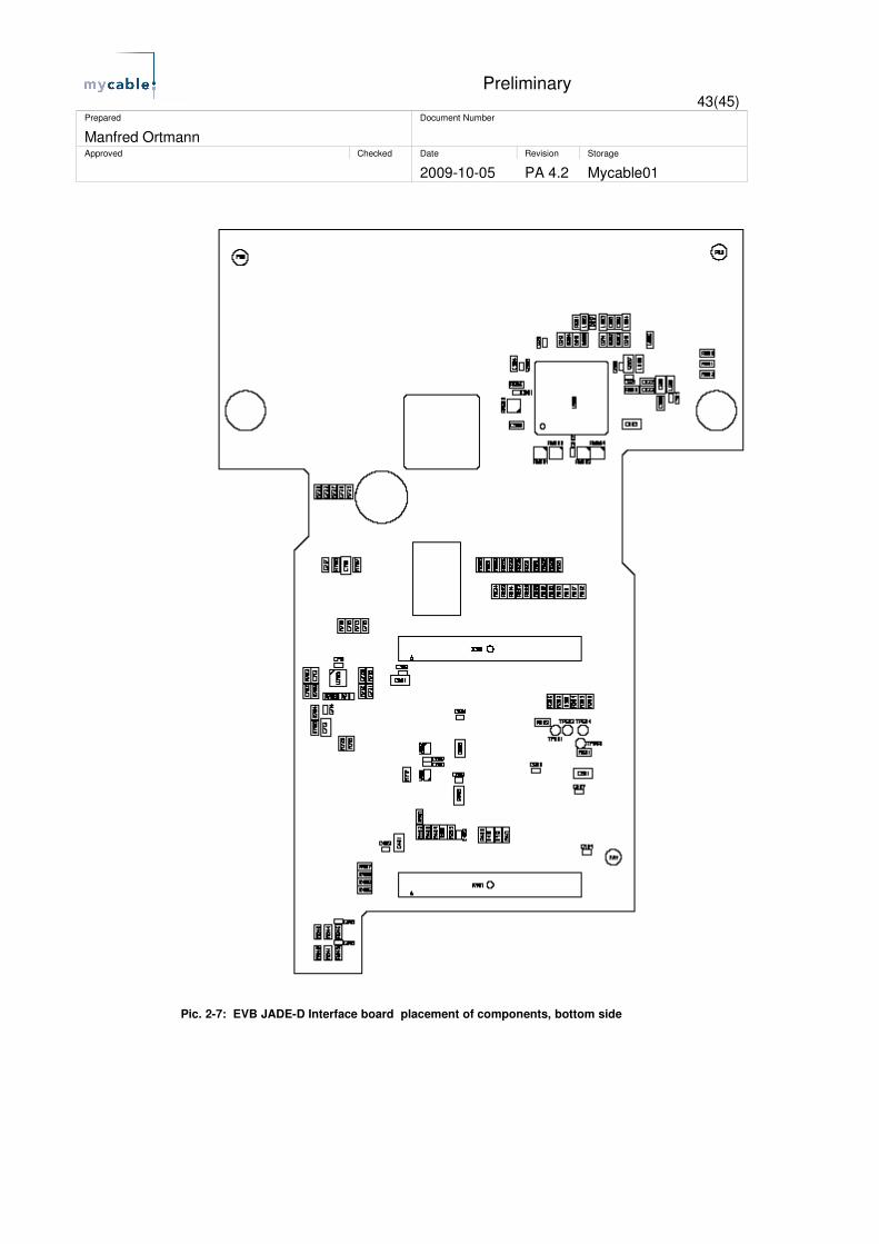
2.4 Placement of Components
The placement of components on the EVB JADED Interface board is shown below.
Pictures from placement of components with a better resolution are available as separate pdf documents.
Pic. 26: EVB JADED Interface board placement of components, top side
Preliminary43(45)
Prepared Document Number
Manfred OrtmannApproved Checked Date Revision Storage
20091005 PA 4.2 Mycable01
Pic. 27: EVB JADED Interface board placement of components, bottom side

Preliminary44(45)
Prepared Document Number
Manfred OrtmannApproved Checked Date Revision Storage
20091005 PA 4.2 Mycable01
2.5 Mechanical Dimensions
The EVB JADED Interface board has a size of 142.0 x 100.0 mm.
Pictures from mechanical dimensions with a better resolution are available as separate pdf documents.
Pic. 28: EVB JADED Interface board mechanical dimensions, top side

Preliminary45(45)
Prepared Document Number
Manfred OrtmannApproved Checked Date Revision Storage
20091005 PA 4.2 Mycable01
Pic. 28: EVB JADED Interface board mechanical dimensions, bottom side