manual pa350 rev 2 pa500.pdf2.6 rf output indicator 8 2.7 over temperature protection 8 3 field...
TRANSCRIPT
Eclipse Series
RF Technology [email protected]
February 2005
PA350/500 Amplifier Operation and Maintenance Manual
This manual is produced by RF Technology Pty Ltd 10/8 Leighton Place, Hornsby NSW 2077 Australia
Copyright © 1997,1998 RF Technology

RF Technology Page 2
CONTENTS CONTENTS
Contents 1 Operating Instructions 4 1.1 Installation 4 1.1.1 Sub-rack Wiring Guidelines 4 1.2 Front Panel Indicators 5 1.3 Internal Adjustments 5 1.4 Amplifier I/O Connections 5 1.4.1 RF Input 6 1.4.2 RF Output 6 1.4.3 25 Pin Connector 6 2 Circuit Description 6 2.1 Amplifiers 6 2.2 Power Splitter / Combiners 7 2.3 Directional Coupler 7 2.4 Low Pass Filter 7 2.5 Power Control Circuits 7 2.6 RF Output Indicator 8 2.7 Over Temperature Protection 8 3 Field Alignment Procedures 8 3.1 Output Power Level 8 3.2 Tuning Procedure 9 4 Specifications 9 4.1 Description 9 4.2 Physical Configuration 10 4.3 Front Panel Indicators and Test Points 10 4.3.1 Indicators 10 4.3.2 Test Points 10 4.4 Electrical Specifications 10 4.4.1 Power Requirements 10 4.4.2 Frequency Range 10 4.5 Antenna Impedance 11 4.6 Output Power 11 4.6.1 Transmit Duty Cycle 11 4.7 Spurious and Harmonics 11 4.8 Heatsink Temperature 11 4.9 ALC Output 11 4.10 Connectors 11 4.10.1 RF Input 11 4.10.2 RF Output 12 4.10.3 25-Pin Connector 12 4.10.4 9-Pin Connector 12

RF Technology PA350/PA500 Page 3
CONTENTS CONTENTS A Engineering Diagrams 13 A.1 Block Diagram 13 A.2 Circuit Diagrams 15 A.3 Component Overlay Diagrams 16 B Parts List 19

Page 4 RF Technology PA350/PA500
1 OPERATING INSTRUCTIONS
1 Operating Instructions The PA350/500 is part of the Eclipse range of modular base station equipment. It is a broadband power amplifier capable of delivering 50 or 100 Watts (depending upon model) in the UHF frequency range. It is designed to complement the T350/T500 transmitter, and mounts in a standard Eclipse sub-rack. 1.1 Installation There are no front panel controls. In normal circumstances no alignment or setup is required. If mounted in a sub-rack that has not previously been wired for a power amplifier, the rack connector must be wired according to the guidelines in section 1.1.1 below. 1.1.1 Sub-rack Wiring Guidelines When installing an Eclipse Power Amplifier in an Eclipse sub-rack, observe the following guidelines for sub-rack installation: • The sub-rack power supply must be capable of delivering the full current
requirements for all modules fitted in the sub-rack, typically 20 Amperes for a 100W transmitter/amplifier.
• Owing to the current drain, power supply lines should be cabled to the power
amplifier separately and using heavy gauge wire to minimise voltage drop and interference via the power supply of other modules in the rack.
• The ALC line from the power amplifier must be connected to the ALC input of the
exciter. If this connection is not correctly made, no control of the output power level will be possible. This can result in excessive RF output power, and consequent breach of licensing authority regulations, or possible overload of the unit. With an Eclipse T500, join pin 8 on the exciter and the amplifier.
WARNING Changes or modifications not expressly approved by RF Technology could void your authority to operate this equipment. Specifications may vary from those given in this document in accordance with requirements of local authorities. RF Technology equipment is subject to continual improvement and RF Technology reserves the right to change performance and specification without further notice.

RF Technology PA350/PA500 Page 5
1 OPERATING INSTRUCTIONS 13. Internal Adjustments 1.2 Front Panel Indicators PWR LED The power (PWR) LED shows that the dc supply is connected to the
transmitter. RFO LED The RF output (RFO) LED indicates that the amplifier is being driven
and that the forward output power is above a preset level. This preset indication level is generally set 1 - 3 dB below the preset output power level. The presetting potentiometer RV2 is not accessible without removal of the cover plate.
TEMP LED The temperature (TEMP) LED indicates (illuminates) should the
amplifier's internal temperature become too high. The RF power is automatically reduced if the internal temperature rises above safe limits.
1.3 Internal Adjustments All internal adjustments are factory set and should not need to be changed under normal conditions. A possible exception to this is the RF output power level which may need to be changed to comply with local licensing requirements. The low forward power warning circuit should be set at the same time as the forward power level.
WARNING Ensure that the power setting complies with the requirements of your licensing authority. Failure to do so may result in penalties being imposed by the licensing authority.
Output Power The output power is set by RV2. This is nominally set to 50 Watts
(+47dBm), but may be set to any value between 20 and 100 Watts depending upon local regulations in the destination country, and the model of power amplifier. RV2 determines the threshold affecting the ALC voltage that is fed back to the transmitter module to regulate RF output power.
RF Level Detector The forward RF power threshold associated with the RFO LED on
the amplifier front panel is set by RV3. This is nominally set at half to three-quarters of the preset output power.
1.4 Amplifier I/O Connections The PA350/500 has three connectors on the rear panel.

Page 6 RF Technology PA350/PA500
2 CIRCUIT DESCRIPTION 1.4.1 RF Input The RF drive is delivered via a BNC connector. The absolute maximum power that should be applied to this connector is 25 Watts. 1.4.2 RF Output The RF output signal is available from an N-type connector. Pins Function 1, 2, 14, 15 Positive supply 12, 13, 24, 25 Ground (negative supply) 8 ALC output
Table 1: Pin connections for the 25 pin “D” connector on the rear panel
Note: The amplifier is capable of delivering as much as 120 Watts continuously. In certain conditions1 an RF power of 130 Watts or more can be available via this connector. This corresponds to peak voltages in excess of 100 while currents in excess of 2 Amperes may flow. Appropriate care should be taken when working on the PA350/500 to avoid making or breaking connections when the amplifier is operating, and to avoid RF burns through close proximity to live connections, etc.
1.4.3 25 Pin Connector The 25-pin “D” connector provides connection to ground and dc power, and from the automatic level control (ALC) circuit. The pin connections are given in table 1. The ALC line floats high to approximately 7Vdc. Pulling this line low will reduce output power. Voltages below 0.5V will reduce the output by more than 20dB. A pull-down current of approximately 1mA is required. 2 Circuit Description The following descriptions should be read as an aid to understanding the block and schematic diagrams shown in figures 1 - 4. 2.1 Amplifiers The RF power amplification is provided by two single transistor amplifiers, Q1 and Q2. Each amplifier is rated at 50 watts output. The input and output impedances of the transistors is matched to 50Ω by broad band microstrip matching networks. The 50W models have only one amplifier fitted. ____________________ 1Excessive powers may be available, for example, in the event of a failure of the ALC loop, such as may arise if the ALC feedback connection is broken.

RF Technology PA350/PA500 Page 7
2 CIRCUIT DESCRIPTION 2.2 Power Splitter / Combiners Trimmer capacitors C10 and C24 are used on the input networks to optimize the input match at center of the desired frequency range. Similarly C58 and C59 on the output networks are used to optimize the output efficiency. Since the design of the amplifiers allows them to be very broad band, they will not usually require re-adjustment unless changing frequency from one end of the band to the other. The dc supply is fed to the amplifiers through resistors R27 and R28. This allows the collector current of each amplifier to be measured at the test socket. 2.2 Power Splitter / Combiners In the 100W models, zero-degree hybrid power splitter / combiners are used to parallel the two amplifier stages. The hybrids consist of quarter-wave 70Ω transmission lines and 100Ω RF resistors CX1-4, R9 and R10. This configuration provides wider bandwidth and better balance than lower cost 90-degree hybrids. 2.3 Directional Coupler The forward and reverse power components are measured through a coupled line directional coupler. The output of the coupled line is frequency compensated by R13, R14, C29 and C30 before being detected by D1 and D2. The output of the detectors is proportional to the forward and reflected voltage components. 2.4 Low Pass Filter A low pass filter consisting of L12 - L14 and C39 - C42 reduces the harmonic components to less than -80dBc. The filter uses a combination of lumped elements and printed microstrips to obtain the required harmonic attenuation. 2.5 Power Control Circuits The forward and reverse voltages from the directional coupler are amplified and inverted by U1a and U1b. The amplified voltages are combined before connecting to the input of error amplifier U1d. Error amplifier U1d compares the detected voltage with the dc reference voltage from output power trimpot RV1. The amplified difference at the output of U1d is supplied to the rear panel system connector for connection to the T500 ALC input.

Page 8 RF Technology PA350/PA500
2.6 RF Output Indicator 3 FIELD ALIGNMENT PROCEDURE Equipment Type Key Specifications Power Supply 13.8Vdc, 15A RF Source 15 Watt (eg. T350/T500 exciter) RF Load / Attenuator 50Ω, 50/100W, SWR<1.2:1 RF Power Meter eg. HP437B or calibrated detector and voltmeter
Table 2: Standard test equipment for the PA350/500 Power Amplifier 2.6 RF Output Indicator The forward power voltage is compared with the pre-set dc reference voltage from RV2 by U1c. The output of U1c is used to turn on the RFO LED and provide an output power logic signal to the test connector. RV2 is normally set so that the RFO LED comes ON 1 - 3db below the nominal power output level. 2.7 Over Temperature Protection Thermistor RT1 is mounted to the case of output transistor Q1. If the transistor case temperature rises above 90 Celsius the resistance of RT1 increases and Q5 is turned ON. This causes the TEMP LED to come on and also reduces the dc reference voltage to the output power error amplifier U1d. The input power will then be reduced by the transmitter ALC circuits and the output transistor is kept within safe operating limits.
3 Field Alignment Procedures 3.1 Output Power Level 1. Set the unit up on a bench with the standard test equipment listed in table 2. 2. Set RV1 and RV2 both fully counter-clockwise. 3. Set the exciter to the desired operating frequency. 4. Adjust RV1 to set the output power on the meter to the level at which you want the
RFO LED to illuminate. 5. Adjust RV2 until the RFO LED just goes out. 6. Adjust RV1 for the desired output power.
RF Technology PA350/PA500 Page 9
4 SPECIFICATIONS 3.2 Tuning Procedure 3.2 Tuning Procedure Adjustment of the matching circuits is carried out with the aim of:
• ensuring that the specified power is available • balancing the load reasonably equally between the power transistors, and • obtaining acceptable efficiency in the power transistors.
Note that the factory alignment procedure is complicated, but allows a given unit to operate across a full 15% bandwidth, without further adjustment. Alignment without appropriate equipment can leave the amplifier unstable or otherwise unable to meet specification. However, the procedure below will usually provide adequate performance. 1. Disconnect the ALC line. 2. Set the RF source to deliver 15W at the highest frequency in the band over which
the PA is specified. 3. Measuring the RF output power, adjust C10, C24, C58 and C59 to obtain maximum
output. 4. On 100W models, measuring the collector currents of Q1 and Q2 at the test socket,
adjust C58 and C59 to reduce and balance the currents, but keeping the power above the required level.
5. Proceed to carry out the power setting procedure in section 3.1.
4 Specifications 4.1 Description The PA350/500 power amplifiers are designed for use with the T350/500 series transmitters to provide 50 or 100 Watts of RF output, depending upon model. Output power is regulated by connecting the ALC output to the ALC input of the driving exciter. The drive from the transmitter module is then automatically adjusted to maintain the required output. The regulated power level can be preset over a wide guaranteed range from 25 to 100 Watts or more, depending on the available input power and the model. Sensing circuits are provided to protect the output transistors from excessive temperature. If the heat sink temperature rises to 80C, the input drive will be reduced to prevent damage.
Page 10 RF Technology PA350/PA500
4.2 Physical Configuration 4 SPECIFICATIONS 4.2 Physical Configuration The power amplifier is designed to fit in an RF Technology sub-rack within a 19" rack frame. The installed height is 4 Rack Units (RU), or 178mm, and the depth is 350mm. The amplifier is 95.25mm or three Eclipse units wide. The amplifier uses an extruded aluminium heat sink with vertical fins. Heatsink temperature rise is typically 20C at 50W output. 4.3 Front Panel Indicators and Test Points 4.3.1 Indicators Power: Green LED RF Power: Yellow LED Over Temperature: Red LED 4.3.2 Test Points Forward Power: Voltage to ground, 0 - 4V, un-calibrated (pin 4 - Gnd) Reverse Power: Voltage to ground, 0 - 4V, un-calibrated (pin 3 - Gnd) Collector Currents: Voltage to positive supply, across 0.1Ω, ±10% (pins 7 - 1 and 8 -1). 4.4 Electrical Specifications 4.4.1 Power Requirements Operating Voltage: 10.5 - 16 Volts, with output power reduced below 12.5V Current Drain: 8 Amperes maximum (7 typical) at 50 Watts and 13.5 Volts, 100mA maximum standby Polarity: Negative Ground 4.4.2 Frequency Range Model Frequency Range PA350A 360-380MHz PA350B 375-400MHz PA350C 330-360MHz PA500A 400-450MHz PA500B 450-512MHz

RF Technology PA350/PA500 Page 11
4 SPECIFICATIONS 4.5 Antenna Impedance 4.5 Antenna Impedance Nominal load impedance is 50Ω SWR 1.5:1 or better. The PA350/500 will operate with a VSWR of 2:1 at all phase angles. The forward power will reduce as reverse power rises above acceptable limits, typically at an SWR of about 2.5:1. 4.6 Output Power Nominally 50/100 Watts, preset adjustable from 15/25 to 50/100. Gain is typically >5dB. 4.6.1 Transmit Duty Cycle The transmitter is rated for 100% duty cycle (continuous operation) at 50W output for air temperature below 40C. De-rate linearly above 40C to 50% at 60C. The transmitter is rated for 50% duty cycle at 100W output for air temperature below 40C. De-rate linearly above 40C to 5% at 70C. 4.7 Spurious and Harmonics Less than 25 µW at any harmonic of the transmit frequency. 4.8 Heatsink Temperature The heatsink temperature can rise to 80C without affecting operation, except for de-rating based on air-temperature as noted in section 4.6.1 above. Shutdown will occur at heatsink temperatures exceeding approximately 90C. 4.9 ALC Output The ALC is intended for connection to the T500. It supplies a voltage which decreases with increasing power or temperature. Voltages below 6V should reduce drive power, at a rate of approximately 6~dB/Volt, with voltages below 1V producing a minimum of 25~dB attenuation. 4.10 Connectors 4.10.1 RF Input The RF drive is delivered via a BNC connector. The maximum power that should be applied to this connector is 15/32 Watts for single/dual transistor models.
Page 12 RF Technology PA350/PA500
A ENGINEERING DIAGRAMS 4.10.2 RF Output The RF output signal is available from an N-type connector. 4.10.3 25-Pin Connector A 25-pin, D-shell (“D”') connector is mounted on the rear panel. It provides power connections and a connection from the automatic level control (ALC) circuit. The pin connections are given in table 1. 4.10.4 9-Pin Connector A front-panel, 9-pin, D-shell connector provides analogue voltages for testing purposes.
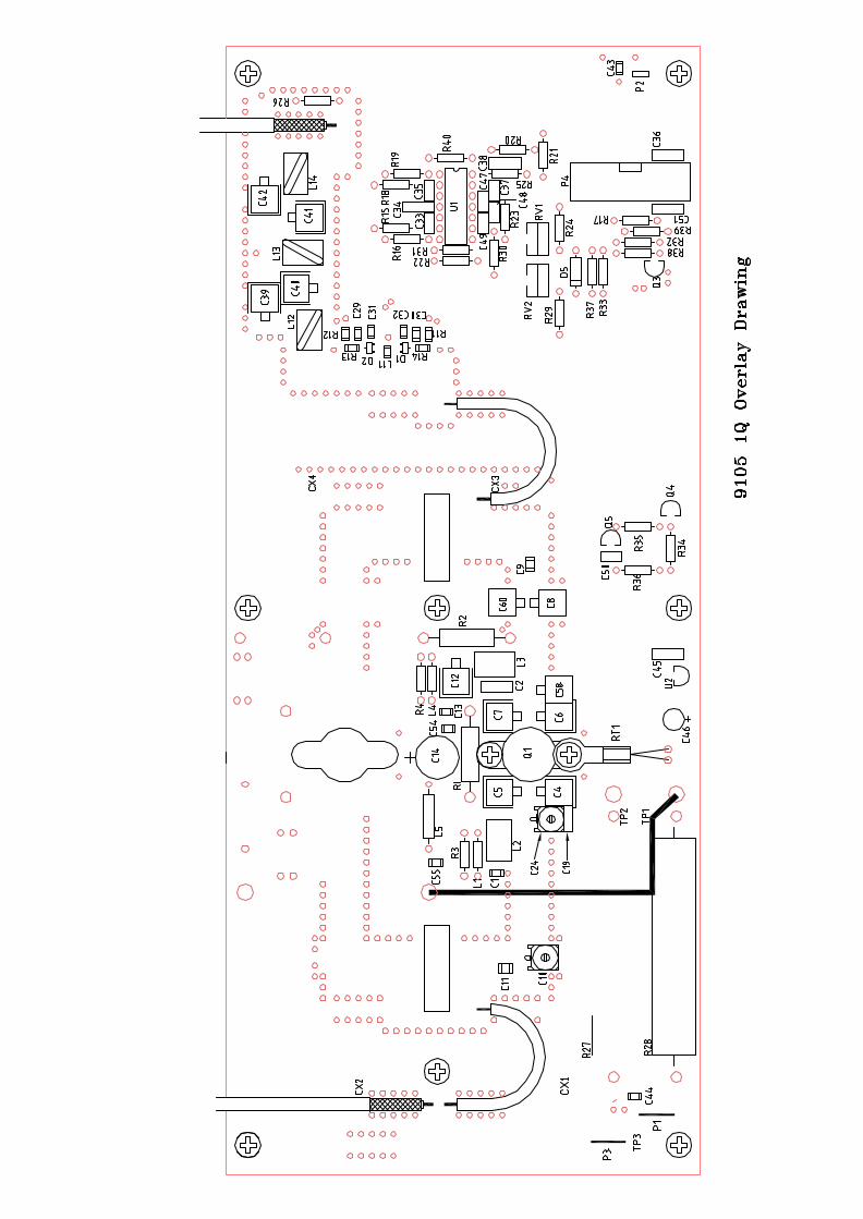
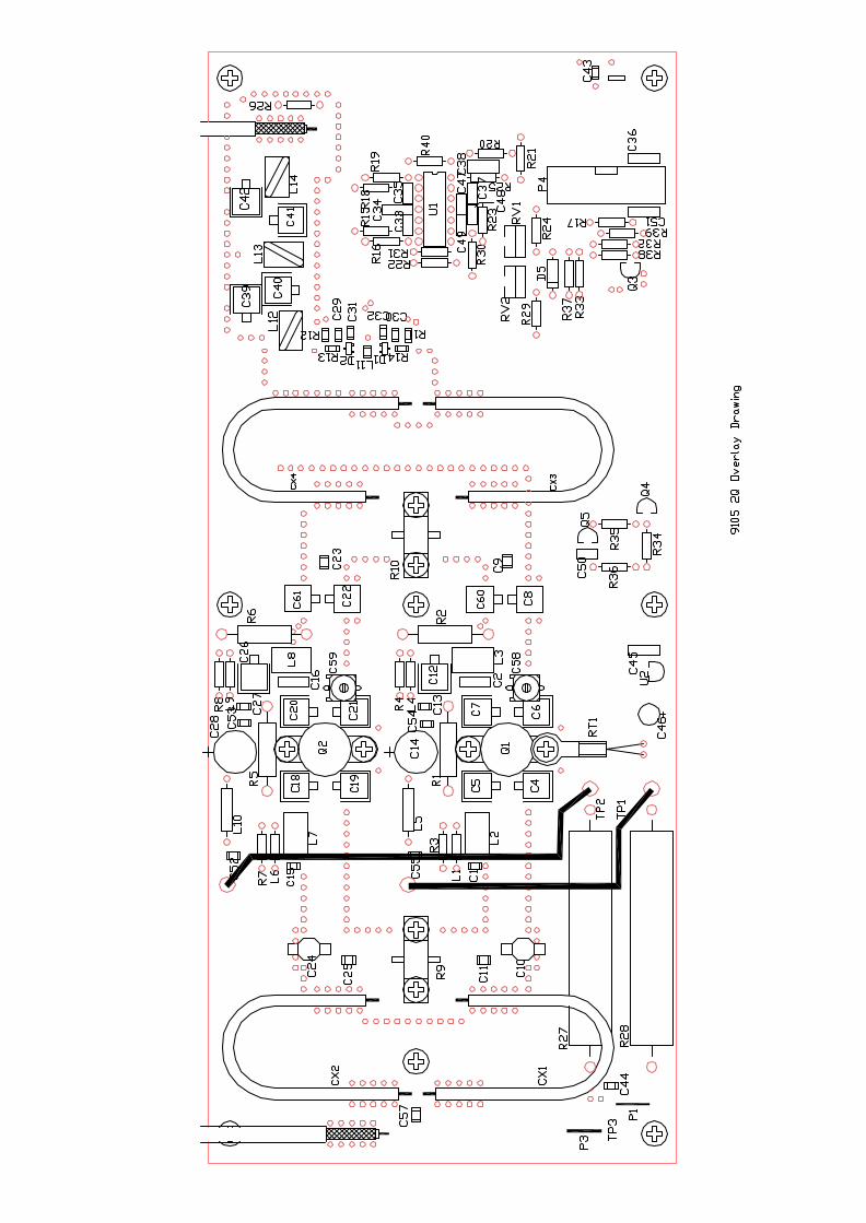
A Engineering Diagrams A.1 Block Diagram Figure 1 shows the block signal flow diagram of the PA350/500 amplifier. Figure 2 shows the chassis wiring diagram of the PA350/500 amplifier. A.2 Circuit Diagrams Figure 3 shows the detailed circuit diagram of the single-stage version of the amplifier with component numbers and values. Figure 4 shows the circuit diagram for the parallel staged version. A.3 Component Overlay Diagrams Figures 5 and 6 show the PCB overlay guides for two versions of the amplifier with component positions.

12
34
ABCD
43
21
D C B ATi
tle
Num
ber
Rev
isio
nSi
ze Orc
ad A
Dat
e:21
-Oct
-200
2Sh
eet
of
File
:D
:\Pro
tel F
iles\
Wor
k Fi
les\
UH
F_M
anua
l.ddbD
raw
n B
y:
-+
+
+8.0
V.R
EF.
POW
ERA
DJU
ST
OU
TPU
T
DIR
ECTI
ON
AL
CO
UPL
ER
FWD
.PW
R.
REV
.PW
R.
U1D
ALC
OU
T
+13.
8 V
dc
U2
++
INPU
T
+8.0
V.R
EF.
U1C
C39
-C42
L12-
L14
SPLI
TTER
CO
MB
INER
D1,
D2
50W
AM
PS
SET
DET
ECT
LEV
EL
R.F
.DET
.
REF
.R
EG.
OV
ER T
EMP.
DET
ECTO
R
OV
ER T
EMP.
ALC
AM
P.
FWD
. & R
EV.
DET
ECTO
R A
MPS
.
CX
1,C
X2,
R9*
CX
3,C
X4,
R10
*
LPF
* N
OT
USE
D O
N S
ING
LE T
RA
NSI
STO
R A
MPL
IFIE
RS
U1B
U1A
Q5
Q4R
V1
Q1
BN
C
RV
2
TEM
P.R
.F.D
ET.
tR
T190
DEG
.C.
Q2*
R F
Tec
hnol
ogy
Pty
Ltd
17/8
Lei
ghto
n Pl
ace,
Hor
nsby
, 207
7, A
ustra
lia
9105
(PA
350/
500)
BLO
CK
DIA
GR
AM
2
11
JBS
afte
r RH
M

12
34
ABCD
43
21
D C B ATi
tle
Num
ber
Rev
ision
Size Orc
adA
Dat
e:3-
Aug
-199
8Sh
eet
ofFi
le:
D:\R
FT_M
aste
rFile
s\..\
9105
-blo
ck.s
chD
raw
nB
y:
AM
PLIF
IER
PCB
ASS
Y11
/910
5
+13.
8
A.L
.C.
0V
PWR
AL
CT
EM
P
LE
DPC
BA
SSY
11/9
106
+13.
8
REV
.PW
R.
FWD
.PW
R.
OV
ERTE
MP.
IcB
IcA
0V RF.
DET
.
INPU
T
OU
TPU
T
13251224112310229218207196185174163152141P5 C
ON
NE
CT
OR
DB
25
J3J1P1
J2P2 P3
12345678910111213141516
P4
12345678910111213141516J5
594837261J6 C
ON
NE
CT
OR
DB
9
D1
D2
D3
+-
+-
+-
J1 BN
C
J2 NTy
pe
R41
100
RF
TE
CH
NO
LO
GY
PTY
.LT
D.
10/8
Lei
ghto
nPL
ace,
HO
RN
SBY
,207
7,A
ustr
alia
9105
(UH
FA
MPL
IFIE
R)
3
33
JBS
afte
rR
HM

RF Technology PA350/PA500 Page 19
B PA350/PA500 PARTS LIST
B - PA350/PA500 Parts List Main PCB Assembly Parts *Denotes location not used in PA350 Ref. Description Part Number C1 Capacitor 1NO 5% 63V NPO SM1206 46/3300/01NO C8 Capacitor 10P 5% 250V MC Mica 48/3002/010P C9 Capacitor Ceramic 220P 5% 500V 100B 46/3100/220P C10 Capacitor Trim 2-18P HI-TMP FLM 49/3001/018P C11 Capacitor Ceramic 220P 5% 500V 100B 46/3100/220P C12 Capacitor 91P 5% 250V MC Mica 48/3002/091P C13 Capacitor 1N0 5% 63V NPO SM1206 46/3300/01N0 C14 Capacitor 6.8U 20% 25V Solid AL 41/2225/06U8 C15 * Capacitor 1N0 5% 63V NPO SM1206 46/3300/01N0 C22 * Capacitor 10P 5% 250V MC Mica 48/3002/010P C23 * Capacitor Ceramic 220P 5% 500V 100B 46/3100/220P C24 Capacitor Trim 2-18P HI-TMP FLM 49/3001/018P C25 * Capacitor Ceramic 220P 5% 500V 100B 46/3100/220P C26 * Capacitor 91P 5% 250V MC Mica 48/3002/091P C27 * Capacitor 1N0 5% 63V NPO SM1206 46/3300/01N0 C28 * Capacitor 6.8U 20% 25V Solid AL 41/2225/06U8 C29 Capacitor 10P 5% 63V NPO SM1206 46/3300/010P C30 Capacitor 10P 5% 63V NPO SM1206 46/3300/010P C31 Capacitor 100P 5% 63V NPO 1206 46/3300/100P C32 Capacitor 100P 5% 63V NPO 1206 46/3300/100P C33 Capacitor 27P 2% 100V NPO Rad.1 45/2680/027P C34 Capacitor 1N0 5% 63V NPO SM1206 46/3300/01N0 C35 Capacitor 27P 2% 100V NPO Rad.1 45/2680/027P C36 Capacitor 10N 10% 50V X7R Rad.2 46/2001/010N C37 Capacitor 27P 2% 100V NPO Rad.1 45/2680/027P C43 Capacitor 1N0 5% 63V NPO SM1206 46/3300/01N0 C44 Capacitor 1N0 5% 63V NPO SM1206 46/3300/01N0 C45 Capacitor 100N 10% 50V X7R RD.2 46/2001/100N C46 Capacitor 10U 35V Rad Electro 41/2001/010U C47 Capacitor 27P 2% 100V NPO Rad.1 45/2680/027P C48 Capacitor 27P 2% 100V NPO Rad.1 45/2680/027P C49 Capacitor 27P 2% 100V NPO Rad.1 45/2680/027P C50 Capacitor 27P 2% 100V NPO Rad.1 45/2680/027P C51 Capacitor 10N 10% 50V X7R Rad.2 46/2001/010N C52 * Capacitor 1N0 5% 63V NPO SM1206 46/3300/01N0 C53 * Capacitor 100N 10% 63V X7R 1206 46/3310/100N C54 Capacitor 100N 10% 63V X7R 1206 46/3310/100N C55 Capacitor 1N0 5% 63V NPO SM1206 46/3300/01N0 C57 * Capacitor Ceramic 56P 5% 500V 100B 46/3100/056P C59 * Capacitor Trim 2-18P HI-TMP FLM 49/3001/018P D1 Diode Schottkey BAT17 SOT23 21/3030/0017 D2 Diode Schottkey BAT17 SOT23 21/3030/0017 D5 Diode Silicon 1N4148 21/1010/4148 L1 Inductor 1uH Axial 37/2021/001U L2 Inductor Moulded 7.5 Turn 37/2021/0007 L3 Inductor Moulded 7.5 Turn 37/2021/0007 L4 Ferrite Bead 3x4x1 4S2 37/1022/0001 L5 Inductor 6 Hole Ferrite RFC 37/1021/0001 L6 * Inductor 1uH Axial 37/2021/001U L7 * Inductor Moulded 7.5 Turn 37/2021/0007 L8 * Inductor Moulded 7.5 Turn 37/2021/0007

Page 20 RF Technology PA350/PA500
B PA350/PA500 PARTS LIST Ref. Description Part Number L9 * Ferrite Bead 3x4x1 4S2 37/1022/0001 L10 * Inductor 6 Hole Ferrite RFC 37/1021/0001 L11 Inductor 1U0 10% Choke SM1206 37/3320/01U0 P1 6.35mm QC Tab Vertical PCB MT 35/0635/0001 P3 6.35mm QC Tab Vertical PCB MT 35/0635/0001 P4 Connector 16 Way Shrouded Header 35/2502/0016 Q1 Transistor NPN 50W RF MRF650 27/3020/MRF650 Q2 * Transistor NPN 50W RF MRF650 27/3020/MRF650 Q3 Transistor GP NPN 2N3904 TO92 27/2020/3904 Q4 Transistor GP PNP 2N3906 TO92 27/2010/3906 Q5 Transistor GP NPN 2N3904 TO92 27/2020/3904 R3 Resistor 10R 5% 0.25W Axial 51/1040/0010 R4 Resistor 10R 5% 0.25W Axial 51/1040/0010 R7 * Resistor 10R 5% 0.25W Axial 51/1040/0010 R8 * Resistor 10R 5% 0.25W Axial 51/1040/0010 R9 * Resistor 100 Ohm 40W RF 51/RF40/0100 R10 * Resistor 100 Ohm 40W RF 51/RF40/0100 R11 Resistor 220R 5% 0.25W SM1206 51/3380/0220 R12 Resistor 220R 5% 0.25W SM1206 51/3380/0220 R13 Resistor 220R 5% 0.25W SM1206 51/3380/0220 R14 Resistor 220R 5% 0.25W SM1206 51/3380/0220 R15 Resistor 47K 5% 0.25W Axial 51/1040/047K R16 Resistor 100K 5% 0.25W Axial 51/1040/100K R17 Resistor 1K0 5% 0.25W Axial 51/1040/01K0 R18 Resistor 47K 5% 0.25W Axial 51/1040/047K R19 Resistor 100K 5% 0.25W Axial 51/1040/100K R20 Resistor 1K0 5% 0.25W Axial 51/1040/01K0 R21 Resistor 100R 5% 0.25W Axial 51/1040/0100 R23 Resistor 47K 5% 0.25W Axial 51/1040/047K R24 Resistor 10K 5% 0.25W Axial 51/1040/010K R25 Resistor 1M0 5% 0.25W Axial 51/1040/01M0 R26 Resistor 100K 5% 0.25W Axial 51/1040/100K R27 * Resistor 0.1R 5% 10W ASW 10 51/0010/00R1 R28 Resistor 0.1R 5% 10W ASW 10 51/0010/00R1 R29 Resistor 10K 5% 0.25W Axial 51/1040/010K R30 Resistor 10K 5% 0.25W Axial 51/1040/010K R31 Resistor 10K 5% 0.25W Axial 51/1040/010K R32 Resistor 270R 5% 0.25W Axial 51/1040/0270 R33 Resistor 270R 5% 0.25W Axial 51/1040/0270 R34 Resistor 10K 5% 0.25W Axial 51/1040/010K R35 Resistor 2K2 5% 0.25W Axial 51/1040/02K2 R36 Resistor 10K 5% 0.25W Axial 51/1040/010K R37 Resistor 10K 5% 0.25W Axial 51/1040/010K R38 Resistor 10K 5% 0.25W Axial 51/1040/010K R39 Resistor 680R 5% 0.25W Axial 51/1040/0680 R40 Resistor 33K 5% 0.25W Axial 51/1040/033K R41(P2) Resistor 100R 5% 0.25W Axial 51/1040/100R RT1 Thermistor 54/0400/0080 RV1 Trimpot 10K 1 Turn Vertical 53/1020/010K RV2 Trimpot 10K 1 Turn Vertical 53/1020/010K U1 IC Quad OP Amplifier TLC274 25/2050/274C U2 IC Volt Regulator 78L08 TO92M 25/2040/78L08

RF Technology PA350/PA500 Page 21
B PA350/PA500 PARTS LIST Ref. Description Part Number PA350A 360 - 380 MHz Parts C4 Capacitor 56P 5% 250V MC Mica 48/3002/056P C5 Capacitor 56P 5% 250V MC Mica 48/3002/056P C6 Capacitor 56P 5% 250V MC Mica 48/3002/056P C7 Capacitor 56P 5% 250V MC Mica 48/3002/056P C19 Capacitor 10P 5% 250V MC Mica 48/3002/010P C38 Capacitor 10N 5% 50V MKT Rad.2 47/2007/10N C39 Capacitor 4P3 5% 250V MC Mica 48/3002/04P3 C40 Capacitor 13P 5% 250V MC Mica 48/3002/013P C41 Capacitor 13P 5% 250V MC Mica 48/3002/013P C42 Capacitor 4P3 5% 250V MC Mica 48/3002/04P3 C58 Capacitor Trim 2-18P HI-TMP FLM 49/3001/018P C60 Capacitor Trim 2-10P HI-TMP FLM 49/3001/010P CX1 RFT CoaxialResonator 37/9105/0001 CX3 RFT CoaxialResonator 37/9105/0001 R22 Resistor 47K 5% 0.25W Axial 51/1040/047K L12 Hairpin, 7.4Dx 20Lx 1.0 37/3002/20DO L13 Hairpin, 7.4Dx 20Lx 1.0 37/3002/20DO L14 Hairpin, 7.4Dx 20Lx 1.0 37/3002/20DO PA350B 375 - 400 MHz Parts C4 Capacitor 56P 5% 250V MC Mica 48/3002/056P C5 Capacitor 56P 5% 250V MC Mica 48/3002/056P C6 Capacitor 56P 5% 250V MC Mica 48/3002/056P C7 Capacitor 56P 5% 250V MC Mica 48/3002/056P C38 Capacitor 10N 5% 50V MKT Rad.2 47/2007/10N C39 Capacitor 4P3 5% 250V MC Mica 48/3002/04P3 C40 Capacitor 13P 5% 250V MC Mica 48/3002/013P C41 Capacitor 13P 5% 250V MC M ica 48/3002/013P C42 Capacitor 4P3 5% 250V MC Mica 48/3002/04P3 C58 Capacitor Trim 2-18P HI-TMP FLM 49/3001/018P C60 Capacitor Trim 2-10P HI-TMP FLM 49/3001/010P CX1 RFT CoaxialResonator 37/9105/0001 CX3 RFT CoaxialResonator 37/9105/0001 R22 Resistor 47K 5% 0.25W Axial 51/1040/047K L12 Hairpin, 7.4Dx 20Lx 1.0 37/3002/20DO L13 Hairpin, 7.4Dx 20Lx 1.0 37/3002/20DO L14 Hairpin, 7.4Dx 20Lx 1.0 37/3002/20DO PA350C 330 - 365 MHz Parts C4 Capacitor 56P 5% 250V MC Mica 48/3002/056P C5 Capacitor 56P 5% 250V MC Mica 48/3002/056P C6 Capacitor 56P 5% 250V MC Mica 48/3002/056P C7 Capacitor 56P 5% 250V MC Mica 48/3002/056P C19 Capacitor 10P 5% 250V MC Mica 48/3002/010P C38 Capacitor 10N 5% 50V MKT Rad.2 47/2007/10N C39 Capacitor 4P3 5% 250V MC Mica 48/3002/04P3 C40 Capacitor 13P 5% 250V MC Mica 48/3002/013P C41 Capacitor 13P 5% 250V MC Mica 48/3002/013P C42 Capacitor 4P3 5% 250V MC Mica 48/3002/04P3 C58 Capacitor Trim 2-18P HI-TMP FLM 49/3001/018P C60 Capacitor Trim 2-10P HI-TMP FLM 49/3001/010P CX1 RFT CoaxialResonator 37/9105/0001 CX3 RFT CoaxialResonator 37/9105/0001 R22 Resistor 47K 5% 0.25W Axial 51/1040/047K L12 Hairpin, 7.4Dx 20Lx 1.0 37/3002/20DO L13 Hairpin, 7.4Dx 20Lx 1.0 37/3002/20DO L14 Hairpin, 7.4Dx 20Lx 1.0 37/3002/20DO

Page 22 RF Technology PA350/PA500
B PA350/PA500 PARTS LIST Ref. Description Part Number PA350D 300 - 330 MHz Parts C4 Capacitor 56P 5% 250V MC Mica 48/3002/056P C5 Capacitor 56P 5% 250V MC Mica 48/3002/056P C6 Capacitor 47P 5% 250V MC Mica 48/3002/047P C7 Capacitor 56P 5% 250V MC Mica 48/3002/056P C19 Capacitor 33P 5% 250V MC Mica 48/3002/033P C38 Capacitor 10N 5% 50V MKT Rad.2 47/2007/10N C39 Capacitor 4P3 5% 250V MC Mica 48/3002/04P3 C40 Capacitor 13P 5% 250V MC Mica 48/3002/013P C41 Capacitor 13P 5% 250V MC Mica 48/3002/013P C42 Capacitor 4P3 5% 250V MC Mica 48/3002/04P3 C58 Capacitor 36P 5% 250V MC Mica 48/3002/036P C60 Capacitor Trim 2-18P HI-TMP FLM 49/3001/018P CX1 RFT CoaxialResonator 37/9105/0001 CX3 RFT CoaxialResonator 37/9105/0001 R22 Resistor 47K 5% 0.25W Axial 51/1040/047K L12 Hairpin, 7.4Dx 20Lx 1.0 37/3002/20DO L13 Hairpin, 7.4Dx 20Lx 1.0 37/3002/20DO L14 Hairpin, 7.4Dx 20Lx 1.0 37/3002/20DO PA500A 400 - 430 MHz Parts C4 Capacitor 56P 5% 250V MC Mica 48/3002/056P C5 Capacitor 47P 5% 250V MC Mica 48/3002/047P C6 Capacitor 47P 5% 250V MC Mica 48/3002/047P C7 Capacitor 47P 5% 250V MC Mica 48/3002/047P C18 Capacitor 56P 5% 250V MC Mica 48/3002/056P C19 Capacitor 47P 5% 250V MC Mica 48/3002/047P C20 Capacitor 47P 5% 250V MC Mica 48/3002/047P C21 Capacitor 47P 5% 250V MC Mica 48/3002/047P C38 Capacitor 100N 5% 50V MKT Rad.2 47/2007/100N C39 Capacitor 3P3 5% 250V MC Mica 48/3002/03P3 C40 Capacitor 10P 5% 250V MC Mica 48/3002/010P C41 Capacitor 10P 5% 250V MC Mica 48/3002/010P C42 Capacitor 3P3 5% 250V MC Mica 48/3002/03P3 C58 Capacitor Trim 2-18P HI-TMP FLM 49/3001/018P C60 Capacitor 3P3 5% 250V MC Mica 48/3002/03P3 C61 Capacitor 3P3 5% 250V MC Mica 48/3002/03P3 CX1 70 Ohm Coaxial Assembly A400 12/0002/A400 CX2 70 Ohm Coaxial Assembly A400 12/0002/A400 CX3 70 Ohm Coaxial Assembly A400 12/0002/A400 CX4 70 Ohm Coaxial Assembly A400 12/0002/A400 L12 Hairpin, 7.4Dx 15Lx 1.0 37/3002/15DO L13 Hairpin, 7.4Dx 15Lx 1.0 37/3002/15DO L14 Hairpin, 7.4Dx 15Lx 1.0 37/3002/15DO R22 Resistor 33K 5% 0.25W Axial 51/1040/033K PA500B 450 - 520 MHz Parts C4 Capacitor 36P 5% 250V MC Mica 48/3002/036P C5 Capacitor 39P 5% 250V MC Mica 48/3002/039P C6 Capacitor 39P 5% 250V MC Mica 48/3002/039P C7 Capacitor 39P 5% 250V MC Mica 48/3002/039P C18 Capacitor 36P 5% 250V MC Mica 48/3002/036P C19 Capacitor 39P 5% 250V MC Mica 48/3002/039P C20 Capacitor 39P 5% 250V MC Mica 48/3002/039P C21 Capacitor 39P 5% 250V MC Mica 48/3002/039P C38 Capacitor 100N 5% 50V MKT Rad.2 47/2007/100N

RF Technology PA350/PA500 Page 23
B PA350/PA500 PARTS LIST Ref. Description Part Number C39 Capacitor 3P3 5% 250V MC Mica 48/3002/03P3 C40 Capacitor 10P 5% 250V MC Mica 48/3002/010P C41 Capacitor 10P 5% 250V MC Mica 48/3002/010P C42 Capacitor 3P3 5% 250V MC Mica 48/3002/03P3 C58 Capacitor Trim 2-18P HI-TMP FLM 49/3001/018P CX1 70 Ohm Coaxial Assembly A450 12/0002/A450 CX2 70 Ohm Coaxial Assembly A450 12/0002/A450 CX3 70 Ohm Coaxial Assembly A450 12/0002/A450 CX4 70 Ohm Coaxial Assembly A450 12/0002/A450 L12 Hairpin, 7.4Dx 15Lx 1.0 37/3002/15DO L13 Hairpin, 7.4Dx 15Lx 1.0 37/3002/15DO L14 Hairpin, 7.4Dx 15Lx 1.0 37/3002/15DO R22 Resistor 33K 5% 0.25W Axial 51/1040/033K

1 2 3 4 5 6
A
B
C
D
654321
D
C
B
A
Title
Number RevisionSize
Orcad B
Date: 21-Oct-2002 Sheet of File: D:\Protel Files\Work Files\UHF_Manual.ddbDrawn By:
FWD.PWR.
REV.PWR.
FWD.PWR.REV.PWR.
IC AIC BRF DET.OVER TEMP.
+8.0
+8.0
+13.2A
+13.8 +13.2A+13.8
+8.0
+8.0
+8.0
+13.8
+13.8
RF DET.
RF LED
RF LED
TEMP. LED
TEMP. LED
DC LED
IC B
OVER TEMP.
LOW PASS FILTER
DIRECTIONAL COUPLER
INPUT
OUTPUT
10W MAX.
50W MAX.
L2
L3
R310
C11
220P
C1291P
L4 C131N0 +C14
6U8
L5
L111U
R11
220
R12
220
R13220
R14220
C29
10P
C30
10P
D2BAT17
C31
100P
C32
100P
R15
47KC3327P
R16
100K
R17
1K
R18
47KC3527P
R19
100K
R20
1KR21
100
C3610N
C3727P
R25
1M
L12 L13 L14
R26100K
J2BNC
TP1
+C4610U
VI1
GN
D2
VO 3
U2LM78L08
C4727P
R3110K
tRT1 C5027P
D51N4148
Q42N3906
Q52N3904
R3410K
R352K2
R3610K
R3710K
C5110N
C54100N
C551N0
C441N0
C431N0
C45100N
C4827P
J1BNC
Q3
2N3904
R410
R28
0R1
TP3
R3810K
C3410N
P1
P2
P3
123456789
10111213141516
P4
R32
270
R33
270
R39680
C1025P
R2910K
RV210K TRIMPOT
R30
10K
C4927P
RV110K TRIMPOT
R2410K
R2347K
L1 1U0
Q1MRF650
D1BAT17
R4033K
R22
33K 5
67
00
+
-
U1BTLC274
2
31
411
-
+
U1ATLC274
12
1314
00
+
-
U1DTLC274
10
98
00
+
-
U1CTLC274 C38
100N
C11N0
C556P
C456P
C656P
C756P C60
10PC8
10P
C242-18P
C394P3
C4013P
C4113P
C424P3
C1910P
C5833P
CX3COAX
CX1COAX
C9
220P
RF TECHNOLOGY PTY. LTD.UNIT 17, 8 LEIGHTON PLACE, HORNSBY, AUSTRALIA
9105 (50W AMPLIFIER, UHF) 4
32JBS after RHM
R41
100
Mounted on P2

1 2 3 4 5 6
A
B
C
D
654321
D
C
B
A
Title
Number RevisionSize
Orcad B
Date: 16-Oct-2002 Sheet of File: J:\L_MASTER_24_04_02\CAD_File\Master_Schematic\Sch_91xx\9105_2Q_ckt.DDBDrawn By:
FWD.PWR.
REV.PWR.IC A
FWD.PWR.REV.PWR.
IC AIC BRF DET.OVER TEMP.
+8.0
+8.0
+13.2A
+13.2B
+13.8 +13.2A
+13.2B
+13.8
+8.0
+8.0
+8.0
+13.8
+13.8
RF DET.
RF LED
RF LED
TEMP. LED
TEMP. LED
DC LED
IC B
OVER TEMP.
LOW PASS FILTER
COMBINER
DIRECTIONAL COUPLER
SPLITTER
** * *
* *
* *
* VALUES SHOWN ARE FOR 450-520 MHZ VARIANT (/4502)
C4 C5 C6 C7 C18 C19 C20 C21 C60 C61
400-430 MHZ (/4002) 56P 47P 47P 47P 56P 47P 47P 47P 3.3P 3.3P
VALUES FOR OTHER VARIANTS
INPUT
OUTPUT
25W MAX.
L2
L3
R3 10
C9
220PC11
220P
C1291P
L4 C131N0 +
C146U8
L5
L7
L8
R710
C23
220PC25
220P
C2691P
L9 C271N0 + C28
6U8
L10
CX1
CX2
CX3
CX4
L111U
R11
220
R12
220
R13220
R14220
C29
10P
C30
10P
D2BAT17
C31
100P
C32
100P
C3327P
R16100K
R171K
C3527P
R19100KR20
1KR21
100
C3610N
C3727P
R25
1M
C393P3
L12
C4010P
L13
C4110P
L14
C423P3 R26
100K
J2BNC
TP1
TP2
+C4610U
VI1
GN
D2
VO 3
U2LM78L08
C4727P
R3110K
tRT1C5027P
D51N4148
Q42N3906
Q52N3904
R3410K
R352K2
R3610K
R3710K
C5110N
C521N0
C53100N
C54100N
C551N0
C441N0
C431N0
C45100N
C4827P
J1BNC
Q3
2N3904
R410
R810
R9100
R10100
R28
0R1
R27
0R1
TP3
R3810K
C341N
P1
P2
P3
123456789
10111213141516
P4
R32
270
R33
270
R39680
C436P
C539P
C10
2-18pF
C639P
C739P
C24
2-18pF
C1836P
C1939P
C2039P
C2139P
R2910K
RV210K TRIMPOT
R30
10KC4927P
RV110K TRIMPOT
R2410K
R2347K
L1 1U0
L6 1U0
C57
56P
C5818P
C5918P
Q2MRF650
Q1MRF650
D1BAT17
R4033K
R22
33K5
67
00
+
-
U1BTLC274
2
31
411
-
+
U1ATLC274
12
1314
00
+
-
U1DTLC274
10
98
00
+
-
U1CTLC274
C2210P
C61*
C810P
C60*
C38100N
C151N0
C11N0
R15
47K
R18
47K
RF TECHNOLOGY PTY. LTD.17/5 Leighton Place, Hornsby, 2077, Australia
9105 (50/100W AMPLIFIER, UHF) 5
31JBS after RHM
R41
100