marantz design and service - archive.org
TRANSCRIPT


ee vr
Using superior design and selected high grade components, MARANTZ company has created the
MARANTZ DESIGN AND SERVICE
ultimate in stereo sound. Only originai MARANTZ parts can insure that your MARANTZ product will continue to perform to the
' gpecifications for which it is famous.
Parts for your MARANTZ equipment are generally available to our National Marantz Subsidiary or Agent.
ORDERING PARTS:
Parts can be ordered a@ither by mail or by telex. In both cases, correct part number has to be specified. The following information must be supplied to eliminate delays in processing your order: 1. Complete address
MARANTZ INTERNATIONAL Vestdijk 9 5600 MD Eindhoven The Netheriands
2. Complete part numbers and quantities required 3. Description of parts 4. Mode} number for which part is required 5. Way of shipment. §. Signature: any order form or telex must be signed
otherwise such part order will be considered as null
and void.
PARTS ORDERING © Parts may be ordared at the following addresses:
AUSTRIA HORNYPHGN Vertriebsgaselischatt GmbH Wienerbergstrasse 1 A1101 Wien: Austria Telex: 132.932
.BELGIUM SVD DIVISILN MARANTZ Industrialaan 1 1720 Groot-Bijgaarden Belgium Telex: 24466
CHILE MARANTZ DIVISION OF PHILIPS S.A. AV. Santa Maria, 0760 Casiila 2687 Santiago Talex: 240.239
DENMARK MARANTZ DIVISION OF PHILIPS SERVICE A/S Praas Boulavard 80 Postbox 1919 DK-2300 Kebenhayn S Denmark Telex: 31201
FINLAND MARANTZ DIVISION OF OY PHILIPS Ab Kalvokatu 8 00100 Helsinki Finjand Teiex: 124811
FRANCE MARANTZ FRANCE
4 Rue Sernard Paiissy 92600 Asniéres France Telex: 611651
GERMANY MARANTZ GERMANY GmbH Max-Planck-Strasse 22 6072 Dreleich 1 Germany Telex: 529821
THE NETHERLANDS Elpro Marantz Wint Hontlaan 28 3526 KV Utrecht The Netherlands Telex: 4748
NORWAY MARANTZ DIVISION OF PHILIPS A/S Sandstuveien 40 0680 Oslo 6 Norway Telex: 72640
GREAT BRITAIN MARANTZ AUDIO U.K. Ltd
- Unit 15/16 Saxen Way industrial Estate Moor Lane Harmondsworth UB7 OLW Great Britain
Telex: 935196
GREECE . SHEATON ELECTRONICS S.A. P.O.Box 21025 Hippocratus Street 188 Athens 11471 Greece Telex: 216.785
JAPAN MARANTZ JAPAN, Inc. 35-1, 7-chome, Sagamiono Sagamihara-shi, Kanagawa Japan
KUWAIT AL, ALAMIAH ELECTRONICS Ussama Building Fahd al Saleem Street P.O.Box 23781 Safat-Kuwait Telex: 22694
ITALY MARANTZ ITALIANA S.P.A, Via Chiesa, 74 20126 Milano Italy
Phone: +31/40.758290 Telefax: +31 /40.75.82.99
SAUDI ARABIA AL ALAMIAH ELECTRONICS P.0.Box 5954 University Street Riyadh 11432 Saudi Arabia Talex: 401530
SOUTH AFRICA MARANTZ DIVISION OF PHILIPS S.A. Main Road Martindale P.O. Box. 58088 Newville 21144 South Africa
SPAIN PHONO S.A. Ignacio Iglesias 10D Badalona (Barcelona) Spain . Telex: 59355
SWEDEN MARANTZ DIVISION OF FHILIPS Forsa!jning AB Tegeiuddsvagen 4 8-115 84 Stockholm Sweden Telex: +4060
Telex: 35000 PHTC NL routing IND NLMTFAT
SWITZERLAND
DYNAVOX ELECTRONICS Route de Villars 105 1701 Fribourg Switzerland Telex; 942377
TURKEY DOGAUOL Lid. LM.C, 6 Biok N°6316 Unkapani Istanbul Turkey Telox: 22085 -
MALTA CACHIA & GALEA Republic Street, 88D Valetta Telex: 1682
PORTUGAL
MARANTZ Divisac philips S.A. service Outurela-carnaxide 2795 LinDA-A-VELHA Telex: 43906
All of the above locations are fully equipped te take care of your total service needs. Because various countries have differing configuration requirements, it is necessary that you contact the service facility in your particular country. In the event that there is no service location listed for your country, please, contact the nearest facility for the necessary
+ Incase of difficulties, do not hesitate to contact the Technical Department at abovementioned address.
assistance.

MODEL CD-94MK2 COMPACT DISC PLAYER
1. P.W. BOARDS
As can be seen from the circuit diagram the chassis of
Model CD-94MK2 consists of the following units. Each unit mounted ona printed circuit board is described within
the square enclosed by a bold dotted line on the circuit
diagram.
‘|
this service manual.
issued by MJ.
common parts”.
PO
a nena e eee Ee Ee re a en ee ae ee ee oe
How to use this service manual
@ The “Common parts” which Marantz Japan, Inc. has established are eliminated from
® These “Common parts” are applied to all models in the service manuals arranged and
@ To indicate clearly the common parts in the schematic diagram, a line is drawn above
or under the Ref. Desig, No. of applicable parts.
@ “Common parts” can be supplied from the Marantz service center as ever. -
In case of ordering, please establish the parts number of 12 N/C’S following the procedure mentioned in this service manual “How to establish the parts number for
1) Please correctly write the parts number of 12 N/C’S following the rule.
1.Demo ............ mounted on P,W. Board PD16
2. Optical Out ........ mounted on P.W. Board PD26 3. Feature u-COM .... mounted on P.W. Board PM16
4, Audic/Power ....... mounted on P.W. Board PP16
5.DAC .......... .... Mounted on P.W, Board PP26
6.3Reg..... Sisligvelanaarsae mounted on P.W. Board PP36
7. Headphone Amp .... mounted on P.W. Board PR16 8. Power Switch ....... mounted on P.W. Board PS16
9. Ten Key ........... mounted on P.W. Board PS26
10. Servo ...........85 mounted on P.W. Board PV16
ti. Servo Module ....... mounted on P.W, Board PV26
12. Photo Reflector ..... mounted on P.W. Board PV36 13. Display ............ mounted on P.W. Board PY16
14. Lamp .............. mounted on P.W. Board PY26
encod sont
ig er ee
MZ 2202

ELECTRICAL MEASUREMENTS AND ADJUSTMENTS
Specification measurement
To measure the specification use can be made of audio test disc 4822 397 30085. Use a 7th order filter, e.g. 4822 395 30204 {see Fig-
ure), to measure: — Total harmonic distortion (THD). — intermoduiation distortion. — Signal-to-noise (S/N).
Laser power supply (POS. VOLT. SH.)
For check and preliminary adjustment of the laser
supply see service manual C.D.M.-1.
Adjusting the laser supply
Play track 1 of test disc 4822 397 300096 {disc with-
out defects). Connect a DC voltmeter across resistor R309 on the servo PCB ( = on emitter of transistor Q315 and
ground). Adjust the laser power supply with resistor 3180 until the voltage across resistor R309 is 575 + 75 mV.
Adjusting the focus bandwidth
R214 A215
{_s7k}
Make a measuring arrangement according to the fig-
ure. Play track 1 of test disc 4822 397 30096 (disc without
defects). Adjust trimming resistor 3158 on PRE. AMPL, + LASER PCB for a 180° phase difference between signals A and B. This corresponds with a minimum distance D
in the Lissajous pattern.
R=47 kQ - 1% 6322 116 54671 C=10 nF -1% 5322 121 54154
MZ 2203 .
Check of the AGC and offset circults (See SERVO PCB) Play track 1 of test disc 4822 397 80096 (Disc without defects). The voltage between pin 7 of IC Q303 (4/4) and L
‘should be -4 V + 2 V. The voltage between pin 8 of IC Q302 (2/4) and 1 should be OV +2 V. ,
?
INITIATION OF THE SERVICING PROGRAMME OF THE uP
— Servicing position “0” Simultaneously depress the STOP, PLAY and SEARCH ex buttons. Keep these three duttons depressed while the mains voltage is switched on.
This is the STAND-BY mode, "0" appears on the
display.
In this state it ts possible to move the arm .by means of the SEARCH FORW and SEARCH REV keys with a minimum torque to the outside and the
inside resp. This enables a check of the free motion of the arm
across the disc.
— Servicing position “1”
From servicing position “Oo” the player can be brought in servicing position “1” by depressing the
NEXT key.
In this state the laser emits light and the objective starts to focus. When the focal point has been reached, “1” appears on the display.
When no disc has been inserted the objective goes 16 x to and fro. Then the player reassumes servicing position "0".
As in servicing position “O" the arm can be moved across the diameter of the disc by means of the
SEARCH FORW and SEARCH REV keys.
— Servicing position “2”
To be reached by depressing the NEXT key after servicing position "1" has been reached.
The turntabie motor starts to run
On the dispiay appears “2",
In preparation of the transition to servicing position
“3” the arm is sent to the centre of the disc.
— Servicing position “3”
To be reached by depressing the NEXT key after
servicing position "2" has been reached.
The radial control is switched on. The subcode information is ignored. MUSB is high so that the music information is released.
On the display appears “3”.

(Dependent on the length of the lead-in track music will be reproduced after approx 1 min}
In this siate it is possible to move the arm by means
of the SEARCH FORW and the SEARCH REV keys to the outside and to the inside resp. Now the motion is controlled by the 4 and the arm moves by steps of 64 tracks as iong as the key is depressed.
if one of the servicing positions 1, 2 or 3 is disturbed
(e.g. braking or removing the disc) the player reas-
sumes servicing position “0”.
The servicing programme can be left by switching the mains switch (POWER ON/OFF) off and on. (Hard-
ware reset).
FAULTFINDING METHOD
Preface
in course of the development of the troubleshooting guide for the Compact Disc it has become clear that a different approach from the one applied so far was required.
For, it is no tonger possible to use the classic strategy,
ie. basing the troubleshooting method on a number of possible fauits in the unit. Practice has shown that a certain fault, with the as- sociated symptom, can have a wide variety of causes.
The reason fs that this player incorporates a num~- ber of feedback loop configurations—which, more- over, might affect each other—and this impedes the obvious measurements.
The method below divides the player from diagram point of view into nine clearly distinguishable sub- groups and by performing some measurements, the
sub-group being in failure can be isolated. Later the defective circuit can be further examined according
to the method given.
PRACTICAL HINTS
Test discs
It is important to handle the test discs with great care. For, the troubles (black dots, fingerprints, etc.) are exclusively and unambiguously positioned.
Damage can cause additional drop-outs etc, and as a result the conscious fault on this disc is no longer
exclusive,
In that case it is no longer possibie to check e.g.
whether the track detector is working correctly.
Measurements on cp-amps
In the electronic circuits of the servo systems op- amps are frequently being applied. These op-amps can be used as amplifiers, as filters, as investors, as
buffers, etc.
In those cases where feedback is appiied in one way or the other, the voltage difference at the differ- ential inputs inclines to zero. This applies both to DC
_ Continuous burning of the laser
> — Disconnect plug J203 on the servo PCB and con-
and to AC. The cause can be traced back to the properties of an ideal op-amp {Zj=~0; G=oo; Z=0). In practice this means that it is nearly impossible to perform measurements on the inverting and non- inverting inputs of op-amps if one input is directly con- nected to ground. In those cases only the output signal will be measur-
abie.
That is why in most cases no AC voltages can be given to the inputs. The DC voltages at the inputs ‘are equal.
Stimulating with “0” and “1”
In the troubleshooting method certain pins shoutd in a number of cases be connected to ground or be
connected to the power supply voltage.
This way of acting offers the possibility to overrule certain circuits and to stimulate others. In this way the diagnose time can be reduced.
in a number of cases the relevant pins appear to be
op-amp outputs,
In this respect it should be mentioned that the outputs of the used op-amps are short-circuit protected.
This implies that the output of an op-amp can be made low ( = usually ground potential) without con-
sequences, On the other hand should be pointed out that it is not ailowed to connect the output of an op-amp directly
to the power supply voitage.
1/Os of microprocessors should not be connected
directly to power supply voltage.
These I/Os are allowed to be brought to “0” in case
this is mentioned explicitly.
Sefection of graund point
It is very important to select a ground point as close
as possible to the test point.
Conditions for injecting
+ {t is should be pointed out that injection of levels or signals from a strange source is never allowed
‘to occur when the power supply voltage is lacking
in the circuit in question. — Naturally, the injected level is never allowed to ex~
ceed the power supply voltage of the circuit in
question.
nect pin J203-9 (laser) of the cable connector to ground. Now the focus loop and the radial loop are inter- rupted as well: J203-7 (RE1 = Radiai Error 1}, J203-8 (RE2 = Ra- dial Error 2) and J203-10 (FE = Focus Error). The taser also burns continuously when the set is
in service loop 2.
MZ 2204

Irregular working of the display
irregular working of the display when the set is opened and playing, might have been caused by inci- dental body effect in the region of the crystal oscil-
jators. Switching “off” and “on” of the mains voltage will elim- inate this effect. a
indication of checkpoint
Inthe circuit diagram the checkpoints have been given a serial number (é.g. A>), to which the troubleshooting
method will refer. For oscillograms, amplitudes, tine bases and position of set, see tables of checkpoints,
GENERAL CHECKPOINTS
In the detailed troubleshooting method following be- low a number of general conditions, required for
proper functioning of the player, will not be repeated.
Before starting the detailed troubleshooting method these general points should be checked.
a. Ensure that disc and objective are clean {remove dust, fingerprints, etc.) and use undamaged discs.
b. Convince yourself of the presence of the clock frequencies, viz.: @ 12 MHz for uP servo (pin 18)
® 11.2896 MHz for FILTER-B IC (pin 19} @ 2.92-5.64 MHz for free-running PLL circuit on
the DECODER-A IC (pin 27) @ 3 MHz for control and display uP (pin 33).
c. Check whether all power supply voltages are present and have the correct level. See PCB drawings.
d. Check whether the two mutes (KILL and MUSB are inactive so that data are nowhere interrupted. This should go high about 2 seconds after the mains voltage is switched on. MUSB=pin 23 of the FILTER-B iC on the decoder PCB. Normally this pin is high during play and low during
search,
DETAILED TROUBLESHOOTING METHOD
A number of quick and efficient checks immediately give a definite answer on poorly functioning sections
of the player. To check the servo systems four service loops have
been built in uP Q271, Before calling in service loops, it should be checked (position power on) whether the bus {clock, data: pin 47 and 10 or 41 of uP Q271 resp) is free. in other words, checking whether these lines do not have a short circuit to ground or supply voitage (ievel low or “high”). In such a case the buttons cannot be oper- ated. For troubleshooting the step-by-step method below is followed,
MZ 2205
First step (with disc on turntable}
Bring the piayer in service loop 1 or 2
If one of the conditions for service loop 1 or 2 is not met, the questions below should be answered posi- tively in the sequence given.
in practice this means that when one question has been answered positively, all the preceding circuits, to which the questions refer, are functioning well,
Example, if the eye pattern is present, we may con- clude that the laser is working, the laser is in focus
and that the turntable motor is running.
Note: In some situations, certain faults in the radial servo circuit affect the focus servo circuit (eg. if supply
' voltage + 1 of IC Q301 in the radial circuit fails, the focus coil starts oscillating). To determine if this situation exists, connect point 4 on the servo PCB to ground. In this way, the influence of the radial servo circuit on the focus servo circuit can be eliminated.
A. is the laser giving light? (Test method: see sub A)
B. Is the angle ‘disc-light pin within the tolerance, ie. 90°+ 05°? (Test method: see description mentioned in chap- ter "Mechanical measurements and adjustments”
of the C.D.M. manua)).
C. Is the laser giving sufficient light? {Test method: see sub C)}.
D. Does the objective come in focus?
{Test method: see sub D)}.
E. Is the turntable motor running and, if so, is it run- ning at the correct speed? {Test method: see sub &)}.
lf the answers to questions 7 or 2 through E are posi- tive, it should be possible to bring the player in service loop 1 or 2.
Second step (with disc on turntabie)
Bring the player in service loop 3.
This means that the eye pattern on point & {on the decoder PCB has to be stable, while MSC on point
<> on the servo PCB has to be more stable too).
{fest method: see DECODER-A IC)
Note that the set is not only tracking a song In loop 3, but also playing the song, provided the digital. circuit is working (however music cannot be hard}.
lf this does not work, return to service loop 2 and an- swer the questions below positively in the sequence given.
F. Are DO and HFL detectors functioning? {test method: see sub F}
G. Is track detector functioning? {test method: see sub G)

H. is the radial control functioning properly? {test method: see sub H}
if the answers to questions F, G and H are positive, it should be possibie to bring the player in service loop
3.
Third step (with disc on turntable)
Note that the set is not only tracking a song in loop 3, but also playing the song, provided the digital circuit is working (music cannot be heard).
If this does not work, return to service loop 3 and answer the question below positively.
|. Is TL functioning, ie. polarity of RE? {test method: see sub |)
J. Is information transmission subcode functioning? (test method: see DECODER-AIC)
Check the Q-channel signals.
If the answers to questions | and J are positive, it should be possible to bring the player in the Play
mode.
Fourth step (with disc on turntable}
if no music is heard in position “play” or service loop 3 answer the last question.
K. Is digital decoder circuit functioning according to specification (test method: see Il. FILTER-B IC and
V. KILL CIRCUIT}
Sub. A. IS THE LASER GIVING LIGHT?
Test method
Bring the player in service Joop 7 without placing a dise on the turntable. Now the laser is giving light for an unlimited period of time.
Another method for which the laser gives light during an unlimited period of time and the objective is stand- ing still, is disconnecting plug J203 on the servo PCB and connecting point J203-9 of the cable connector to ground. In case of power-on the laser should burn. This is checked with the aid of a light-sensitive component which is slightly screened from ambient fight.
Hereafter follow some examples:
a. Connect photosensitive diode type BPW4, code number 4822 12032108, with correct poiarity to an analogue multimeter (e.g. PM2412) at range 10
kQ. if the laser is burning, the meter will give virtually full scale deflection.
b. Connect LDR, code number 4822 416 10002, to digital multimeter PM2517E. If the laser is burning, the resistance will drop to
approx. 8 kQ.
if the laser is not giving any light, proceed to Annex 1.
Sub. C. IS THE LASER GIVING SUFFICIENT LIGHT?
Test method (Test points on Pre-amp PCB)
— Interrupt the collector of Q203 on the servo PCB
or ground -the-side of electrolytic capacitor C201. Disconnect plug J203 on the servo PCB and con- nect pin J203-9 (laser} of the cable connector to ground.
Now the faser should continue to give light while FE, RE1 and RE2 are interrupted.
— Place disc on turntable and switch power on.
— Directly inject with AF generator (Z, = 600 Ohms) to test point <> FE a sine-wave signal between 25 and 60 Hz (exact frequency is player-dependent) and 2Vpp.
— Select such a frequency that the monitor diodes of the light pin give output signais as indicated on test points >, ©, @ and @>. Amplitude 40-80 my.
— if the amplitude is not sufficient, proceed to Annex
1.
Sub, D, IS THE OBJECTIVE COMING INTO FOCUS?
Test method
@ No disc on turntable
Switch power on and actuate Play button. Now the arm should move inwards. Immediately af-
ter that the objective should move two times up-and downwards (this happens during searching of the fo-
cusing point),
After this the action will stop.
These actions are software-controlled from the servo uP. If this is not working, check uP servo, end stage focus circult or focus coil.
@ With disc on turntable
Quick test procedure:
For a rough check on the working of the focus circuit, proceed as follows: — place disc on turntable. -— set player in service foop 1.
— remove disc from turntable. — now examinate if the objective focuses by bringing
a reflective object (e.g. mirror) above it.
Detailed test procedure
— Check @203 (on servo PCB) as follows: Check whether FN becomes, with each passage of the nominal focusing low for a short period of time. Only when focusing point FN has been found, FE will be released via Q203 {base will be-
come negative). Check whether base of Q202 is driven low from servo uP (= FCO). If not, check servo uP. If so, proceed,
— Test focusing circuit as follows: Interrupt the collector of Q203 on the servo PCB and disconnect plug J203 on the servo PCB. Con-
MZ 2206

nect pin J203-9 (laser) of the cable connector to ground. Now the laser is burning continuously, FE has been
released and the focus loop has been interrupted at test point <> (=FE) on servo PCB.
Testing of circuit, between test point <> and focus- ing coil (Test points on servo PCB)
— Directly inject a sine-wave signal of 10 Hz, 2Vpp, to test point <> by means of an AF generator {Z; = 600 Q).
— Check visually whether focusing coil “--" and thus objective too “--" responds,
— Check whether this voltage is 0.6 Vp, on test point
_ Check whether this voltage is 6 Vp, on test point
— Check whether this voltage is 5 Vpp on test point
Testing the subchassis (Test points on Pre Amp PCB, injection point on servo PCB)
— Place a disc on the turntable. ‘
— Directly inject to test point <> a sine-wave signa! between 25 Hz and 60 Hz at 2 Vpp, by means of an AF generator (Z, = 600 9). The exact frequency is player-dependent.
— Select such a frequency that the monitor diodes of the light pin give output oa as indicated on test points @, @, <P and @®.
— Check test points @, &, <> and <>.
— Check test point <>. — Check test point @.
Is the same as signal on test point a> but am- plitude is dependent on position of potentiometer
3138.
If all the checks are positive, close focus loop (insert plug J203). Now the focusing circuit should be able to operate. Reconnect transistor Q203.
It should be noted here that the amplitudes on test points & through <> are slightly dependent on the charactéristic of the monitor diodes.
Sub. E. IS TURNTABLE MOTOR RUNNING AND, IF SO, IS IT RUNNING AT THE CORRECT SPEED?
Test method (Test points on servo PCB)
~— Place disc on turntable and bring set in service loop 2.
— If focusing point is found, check whether FCO is low on point
ff not, check focus circuit sub D, If so, proceed.
-- Now only power on, disconnect plug J201 on the servo PCB and check MSC=point 4 of cable con- nector J201 or point > on the decoder PCB.
MZ 2207
if not, check Decoder-A !C (Q504) circuit. if so, proceed.
— Reconnect plug J201, disconnect plug 15 on the preampiifier PCB and inject a DC signal to the cabie connector of the motor or directly to the turntable motor. The turntadle motor should be running now. {A DC voltage of 2,5 V approximately corresponds with the rpm during scanning of the innermost
tracks}. In this condition the player should be brought in service loop 2 (depress: Stop button while mains voltage is switched on). if DC < 2.5 V Figure G should be visible on test point {> (serve PCB), if DC > 2.5 V Figure H should be visible on test point <>
If so, check turntabie contro} circuit (circuit from point <> to turntable motor). If not, check whether MSC is released by means of SSM at pin 16 of IC Q271., This connecting plug J201 on the servo PCB and measure on pin 12 of cable connector J201. If MSC is working now, check circuit around IC Q271.
— Take player out of service loop 2, depress Power- on button and then Play button and check eye pat- tern on point €} (on decoder PCB). To stabilize the eye pattern, bring light pin above tracks by hand, or by briefly (6 s} depressing Fast Forward button.
If eye pattern not point is not present or un- stable, check RF pre amptifier {see Annex !V).
— If eye pattern is correct, proceed.
— Check whether point > {=HFLS} on the servo PCB is correct in service loop 2 (see Figure Y). If not, check HFLS detector circuit (is circuit between point €> and $3), If so, proceed.
Take player out of service loop 2 by depressing the power button.
— Check locking-in of PLL circuit of Decoder-A IC.
(See CEFM signal pin 27: point €) If PLL is tocking-in, proceed.
— Check timing signals on output of Decoder-A IC as indicated in "DECODER-A IC", Is the digital decoder circuit functioning accord- ing to specification? If timing signals are correct, proceed.
— If MSC is still not functioning properly, replace the relevant specific digital IC according to the trial and error method with the aid of service IC box.
— MSC has to be present now.

Sub. F. ARE THE DO and HFLS DETECTORS FUNC-
TIONING?
Test method (Test points on servo PCB)
— Starting point is: HELS = 1 when spot is exactly ontrack
HELS = 0 between tracks (e.g. during track jumping)
DBO = 0, or DO = 1 in case of drop-out
DO = 1, or DO = 0 when there is no drop-out.
Approximative method {applicable in service loop 2)
— Place disc on turntable. — Bring player in service loop 2.
— Check whether DO {test point > is not continu-
ously "high". Normally test point is “low”, how-
ever smali spikes of approximately 100mV are pre-
sent in case of scratches on the disc,
— Check HFLS (test point 63).
Precise method (can be checked in playing set only)
_- Place test disc 5A on turntable. Switch power on
and depress Play button.
— Select track no. 10; Check point . HFLS pulses should be present,
— Select track no. 15; Check point 6. DO pulses should be present. With this track the
FIFLS pulses on point 6 should also be present.
_—. In case of track jumping HFLS pulses are always
present on point €.
Sub. G. 1S TRACK DETECTOR FUNCTIONING WELL?
Test method (Test points on servo PCB)
Switch off the offset circult:
Loosen resistor 3315 {at the side where it is incontact
with pin 8 of IC Q302).
Mount a 47 kQ trimming potentiometer between +i
and -1 supply voltage (for example between pins 4
and 11 of IC Q302), Connect the wiper of the trimming
potentiometer to the loose side of resistor 3315.
— Place a disc on the turntable.
— Bring the set in service loop 2.
— Adjust the signa! on test point symmetrically
round OV by means of the external 47 kQ trimming
potentiometer. The amplitude of the signal may
change during this adjustment.
— Measure F.S on point $8. Here too the frequency variation depends on the
eccentricity of the disc.
— Check point €o. .
— Check point €}. Signal cannot be triggered.
— Check point €>. — Switch the offset circuit on again.
Sub. H. IS THE RADIAL CONTROL FUNCTIONING PROPERLY?
Attention: The offset clrcult (d-multipuiler) and the AGC circuit (k-multiptler} are correction circuits. This means that under optimal conditions (new disc, minimum tolerances of components) the set may be working properly even if a fault is preset in offset
or AGC circuit.
Test method (Testpoints on servo PCB)
a. Place disc on turntable. b. Switch off AGC circuit (k-multiplier) and switch off
offset circuit {d-multiplier).
Method:
Switching off AGC circuit: interconnect points > and @> of IC Q309.
— Place a disc on the turntable. — Bring the set in service loop 2. — Adjust the signal on test point symmetrically
round OV by means of the external 47 kO trim- ming pot. The amplitude of the signal may change
during this adjustment.
c, Bring set in service loop 3. At this moment there is a high probability that the
set is working. If so, check d and k factor {see Annexes Il and ill).
if not, proceed,
d, Bring set in service loop 2 and check signal on
point <p. The AC-component has to be 12-14 V symmetri-
cally, around a DC level of zero volt.
If this is correct, proceed to e}. If this is not correct check following testpoints
&>, €}: value should be 0.7 Vpp €>: value should be 0.2 Vpp @>: value should be 0.25 Vpp @; value should be 20 MVpp $d, €: value should be 800 mVpp
Note: The frequency variation strongly depends on the eccentricity of the disc. If points € + €B are OK, check point €> again. if €> is OK, proceed.
e. Check paint € (is RE + 650 Hz). Value should be Vpp if so, proceed.
When the set is in the normal stand-by position 650 Hz at 300 mV is present on point @%.
cal _ To check radial output stage, do not use a disc, only power on. Inject on points €> and Sp respec - tively a sine-wave signal of 8 to 10 Hz 3 Vpp. Then the radial motor will go back and forth.
At this moment radial tracking must be possible in ser-
vice loop 3. — Switch the AGC circuit on again.
If the original fault symptom is still present proceed
MZ 2208

to Annex Iil:
Check of the k-factor. — Switch the offset circuit on again,
If the original fault symptom is still present, pro-
ceed to Annex Il: Check of the d-factor.
Sub. |. IS INT FUNCTIONING, O.E. RoE OF RE? (Measure points on servo PCB)
Test method Bring player in service loop 3 and measure INT on pin
12 of uP servo IC Q271.
A square-wave voltage (0-5V} should be measured on th is pin. As a result of the frequency variation th is
square-wave is hard to trigger.
| DECODER-CA IC
@ Check the MC signal (pin 17; test point <p) — In stand-by mode, the MC signal (Motor Control)
corresponds to the figure below.
Nofe:
The repetition time of the MC signals is 11.3 usec.
— Place a disc on the turntable. — In position PLAY or SERVICE POSITION 3, the MC
signal corresponds to the figure below.
Note; During start-up the duty cycle is 98%, then the duty cycle of the signal becomes about 50%.
See also Service Manuai CDM-1: “Check of the motor
control”,
POSITION: STANO BX
ag POSITION: PLAY [8EGHPNG)
Eanes POSITION: PLAY [NORMAL
@ Check the HF signal on test point €> (eye pat- tern}
— Place a disc on the turntable. — The HF signa! should be present and be stable in
the PLAY mode and in: SERVICING POSITION 3 after the run-in track has been read.
— In SERVICING POSITION 2 and during reading of the lead-in track the HF signai is not stable.
Position of oscilloscope 0.5 us/DIV.
Amplitude = 1.5 V,,
MZ 2209
Check the HFLD signal on test point €&
Place a disc on the turntable.
In the PLAY mode and in SERVICING POSITION 3 the HFLD signal is “high”; however, minor pulses may be present and in cause of disorders on the
disc.
— In SERVICING POSITION 2 and during playback of track no. 15 of test disc 5A HFLD pulses are
visible,
Position of the oscilloscope 5 ms/DIV
HFLD ee ee ep |
@ Check If the MUTE signal (pin 11; test point €>) is “high” When Filter-B IC is applied, the MUTE input will not
be used.
@ Check the CEFM signal (pin 27; test point <9) — Place a disc on thr turntable.
— In stand-by mode {only the main s switch is de- pressed}, the frequency lies between 2.82 MHz and 5,64 MHz. --
— In the position PLAY and SERVICE POSITIONS 2
and 3, the frequency is 4.32 MHz.
Check the Xin signal (pin 19; test point <3} — The Xin frequency is 11.2896 MHz.
— If this frequency deviates, check test point 70; Xout signal, on Filter-B IC. This frequency should also be 11 2896 MHz.
@ Check the timing signals meant for Filter-B IC
— Place a disc on the turntable. — Select one of the following positions:
SERVICE POSITION 2 or 3, or position PLAY. — Trigger the oscilloscope with the WSAB6 signal
(test point ¢}, pin 39}. — Check signals:
WSAB at test point <> {pin 39) (Word Select from Decoder-A to Filter-B}
CLAB at test point ¢B {pin 38) (Clock from Decoder-A to Filter-B)
and their interrelation,
~— There must be activity at test point (pin 37}, DAAB signal (DATA from Decoder-A to Filter-B).
fy colle cel

Check the EFAB signal (Error Flag from Decoder- A to Filter-B) at test point <> (pin 36)
Place test disc 5A on the turntable. During playback, EFAB fulses should be present at test point <> for soft braking of the disc and during fast search (F.Forward, F.Reverse).
Note: filter-B IC is capable of interpolating linearly 8 successive EFAB pulses.
_ sample interpolation
N
interpolation ) period
EFAB (error flag) | | i ] | | | |
Check the Q-channel signals Place a disc on the turntable. Select one of the following positions: SERVICE POSITION 3 or position PLAY.
Trigger on the QRA signal (Q-channel Request Ac- knowledge) test point <; pin 30. Check signals QRA at test point ¢> (pin 30).
QCL at test point <® (pin 31). (Q-channel-clock)
and their interrelation. There should then be activity at test point ¢> {pin 29) QDA (Q-channel Data}.
Note: The QRA request is initiated by decoder uP {QRA “high”, Then Decoder-A answers this request (QRA goes “low”). With the next leading clock
pulse (QCL) the QRA signal is rendered “high” again
by the decoder iP. AS soon as the decoder :P has taken in enough information via QDA, QRA will go low again. That
is why the QRA times vary each time.
ora if |
om f
Alea nore esac acest arenes ae
Check the SSM signal (test point ¢3; pin 33) = Start-Stop turntabie motor
Motor start pulse when test point ¢® is “high” for = 02 sec. Motor start pulse when test point > is "low" for
= O02 sec.
Note; After the motor start pulse, SWAB information
(Subcoding Word clock) will become visible at this point. The period time of that signais is 136 usec.
Check the subcode clock signals
Place a disc on the turntable. Select one of the following positions: SERVICE POSITION 3 or position PLAY. Trigger the oscilloscope with the SWAB signal at
test point <. Check the following signals:
SWAB at test point <a pin 33 SCAB at test point ¢>; pin 35 (Subcode Clock
from Decoder-A to Filter B) SDAB at test point €9; pin 34 (Subcode Data from Decoder-A to Filter B)l
and their interrelations.
Nofe: While the burst of 10 clock pulses, appear on SCAB the Q-channel information is transferred on SDAB. Hereafter the P-bit indication follows. The P-bit “high” between two bursts of 10 clock pulses in case of pause indication and "low" in
case of music indication,
SWAB
[i LS, ed ee
SCAB
(92, 8224MHz
SOAB ears
Check the CRI signal
The CRI is “low” in case of track jumping. Player in position SEARCH.
Check the DEEM signal (test point $y; pin 32)
Place test disc 5 on the turntable. During playback of track no, 14 (recorded without PRE-EMPHASIS), the DEEM signal should be "low". During playback of track no. 15 (recorded with PRE-EMPHASIS), the DEEM signal should be "high",
MZ 2210

it FILTER-B IC
e@ Check the signals between Decoder-A IC and Filter-B IC
See sub, "] Decoder-A IC",
— Check the X IN signal (test points €> and ¢) — Check the timing signals meant for Filter B
(WSAB, CLAB, DAAB signals; test points ¢}, <> and @>}.
— Check the EFAB signal {test point ¢}) .
— Check the subcode clock signals (SWAB, SCAB, SDAB signais; test points ¢}, ¢} and €).
@ Check the timing signals between Filter-B IC and DAG IC
-- Place disc on the turntable. — Select one of the following positions:
SERVICE POSITION 3 or position PLAY. — Trigger the oscilloscope with the WSBD signal
(Word Select from Filter B to DAC) test point <> {pin 18},
Check the following signals: WSBD at test point €}; pin 18 CLBD at test point >; pin 16 (Clock signal from Filter B to DAC) and their interrelation.
If an Audio disc is used, there should be activity at test point (pin 15) DABD signal {DATA from Filter B to DAC). If a disc with Digital Data {CO-ROM) is used, this point is continuously switched “low” by transistor Q537. In that case the word “data" appears on the display.
ee a Ta |
5 SeccgMHz :
__283,5, 235,
e@ Check the DOBM signal (Digital Gutput)
— Place a disc on the turntable,
— Select the stand-by mode (only mains switch de- pressed).
— Trigger the oscilloscope with the SWAB signal {test point £8).
— Check the DOBM signal (test point 8; pin 14). An empty audio signal has a fixed pattern, See drawing, “Stand-by”,
— Select the PLAY mode. Check the DOBM signal. See drawing “PLAY”.
a i = AUUUO TC UU
eae anes | © TT.
MZ 2214
@ In position SEARCH the ATSE signal is “iow” test point €; pin 22 (Attenuation Audio Signal)
— When the “uP panel” is applied, (a sub-printed cir- cuit board} that houses IC Q271, test point &> is not connected.
@ Check the MUSB signal test point <0; pin 23 {Soft Mute} This signal is “low” in positions: PAUSE NEXT or PREVIOUS when jumping form one track to another, Fast SEARCH when the Search button is kept de- pressed for some time.
It DAC IC {Dual Digital Analog Converter)
@ Check the signals between Filter-B IC and DAG Ic
See sub, “ll Filter-B IC": — Check the timing signals between Filter-B !C and
DAC IC,
@ Check the output of the OP-AMP after the DAC Ic
— Place a disc on the turntable.
~~ in position PLAY or in SERVICE POSITION 3, the analog (music) signal should be present at the out- put of the OP-AMP, after the lead-in track has been read.
IV DEEM CIRCUIT
@ Check DEEM circuit
— Place test disc 5 on the turntable.
— During playback of track no. 14 (recorded without PRE-EMPHASIS) the DEEM signal at test point > should be “low”.
— During playback of track no. 15 (recorded with PRE-EMPHASIS), the DEEM signal at test point €> should be “high”,
— During playback of track no. 14 the analogue sig- nal shouid be present at the source of R564 {test point €}) and R565 (test point <2),
— During playback of track no. 165 the anaiog signal at the source of R564 {test point > and R565 (test point €3) should be 0 V.

V KILL CIRCUITL
— During switching on and off the mains voltage the signal on the collector of QNOt and QNO2 should be as indicated in the figure below.
4,8V 4.8V
QNO1 ‘ OV
1
12 2 SEC ‘
l
POWER ON POWER OFF
4.8V
ene OV
i I l | ! I t
=
av
VI FAVOURITE TRACK SELECT (FTS)
Attention: When repairing a CD player it is important that the cxontents of the FTS memory (EEPROM) should not
unnecessarily be damaged. If no complaints are reported about the functioning
of the FTS, a check of the functions of the EEPROM
should be left undone. The EEPROM IC is in the Stand-by mode when CE and RDY are both high.
Selftest of the FTS pP
During the self-test of the FTS uP, 1/0 Gate will not be tested. Therefore this self-test can be executed without dam- . age to the memory as indicated in Generai Test Points.
Annex | LASER IS GIVING NO OR INSUFFICIENT
LUGHT
Fogether with laser supply and the monitor diode the
laser forms a feedback system. A defect in the laser suppty might thus result in-de- struction of the laser. Replacement of th laser (=new light pin) will not solve anything. The new laser will also be destroyed since the original fault in the laser supply is still present.
On the other hand it is impossible to check and repair
a feedback system when one link is missing.
For this reason the so-called laser simulator 3 is sup- plied. Code number 4822 395 30229. This laser simulator consists of a PCB which contains the laser and monitor simulation, a switch to test the On/Off position and a number of sockets.
10
This PCB can be connected to the laser supply in- stead of the light pin so that the feedback system is closed.
Repair procedure:
Since the light pin is very sensitive to static charg- es, care should be taken that during measurements and adjustments of the laser power supply the po- tential of the aids and yourself equal the potential of the CD mechanism.
Detach light pin an conneet laser simulator as follows:
(connections on pre-amp PCB8). Take the flex PC8 out of socket 11 and connect the
simulator PCB with the socket. Remove plug 16 and insert it in the socket on the
simulator PCB, Connect the plug with 4 wires to socket 16, Take out plug 17 and insert the plug with 1 wire in socket 17.
— Switch on the mains switch and ensure that the drawer is closed or else that the tray-end-in switch on the tray PCB (S004) is depressed. Now press the play key and check if the L-line of
the servo mP, pin 21-2 on the pre-amplifier PCB,
goes "low". In rest position the current through the laser diode should be = 1 mA. For NEG. VOLT. lasers this can be checked as follows: Set the switch on the simulator PCB in the OFF position and the mains switch in the ON position. Turn trimming resistor 3180 counterclockwise (min. R) and measure the voltage across resistor 3194 on the pre-amp. PCB. On pre-amplifier PCBs with discrete components turn resistor 3180 clockwise (min. R) and measure the voltage across resistor 3194, The voltage should be = 15 V.
Check of laser supply control
Set the switch on the simulator PCB in the ON position and measure the voltages between points +V and=V on the simulator PCB. . Resistor 3180 clockwise {max. R): U,y..=225 mV +45 mV, On pre-amplifier PCBs with discrete components resistor 3180 counterclockwise {max. R): Uyy-y=225
mV +45 mV,
R3180 counterclockwise (min. R): Uyy.y=750 mV + 150 mV. On preamplifier PCBs with discrete components re- sistor 3180 clockwise (min. R): Ugy-y=750 mV +150 mv.
Set resistor 3180 in the mid-position. This is a preliminary adjustment. After the simulator PCB has been removed the laser current must be ad- justed,
Fine adjustment of laser current
— Playback track 1 of test disc 4822 397 30096 (Disc without defects), Connect a DC voltmeter across resistor 3308 on the SERVO PCB circuit
MZ 2212

diagram D. Adjust the laser power supply with re- sistor 3308 is 575 mV + 50 mV.
Annex Il: CHECKING d-FACTOR {Test points on servo PCB)
-—- Switch off AGC circuit (k-multiplier) and switch off offset circuit (d-multiptier). See sub G and H.
Place disc on turntable and set player in service loop 2.
— Check points € and @. Value should be 0.7 Vpp. Frequency variation strongly depends on the ec- centricity of the disc.
—- Check points Value should be 250 MV pp.
— Check point €. Value should be 200 MVpp-
— Check point Value should be 2 Vop.
— Check points and Value should be 10 Vpp. The signals is more sine~shaped now due to fil- tering out of 650 Hz.
— Point € is hard to measure since switch is in posi- tion Yor and thus connected with input of op-amp Q302 (pin 9). However, a signai of 200 mVpp is present.
— Check point Value should be 9 Vpp.
Bring the playér in service loop 3, With a disc on turntable and the AGC and offset-circuits are still switched off. — Check point
~- Check point check point oscilloscope is triggered with point
— Switch on the AGC-circuit and offset circuit.
on :beam A of oscilloscope and
Annex ill: CHECKING k-FACTOR (Test points on Servo PCB)
a. Static
Switch power on without depressing the Play button.
Le. RCO=high; ROO=iow so switch Ya is in position 0 and switch Yc is in position 0. — Check point @>.
Value should be 9 Vpp. — Check point — On point now appears a sine-wave signal of
650 Hz, 300 mV, and 180-45=360°shifted in phase relative to signal on point €>.
— Check point <>. Value should be 1.5 Vpp.
— Check point Value should Be 1 Vopp
— Check points >, &, } and & relative to each other, Amplitudes are BV.
— Check integrator IC Q303 (4/4}
MZ 2213
on beam B of oscilloscope while.
_ signal on point
b. Dynamic
Insert disc, select service loop 2 and check if the > equals to 7 Vp.
— Select service loop 3. Now RCO=shigh and RCO=!ow. So switch Y, is in position1. Switch Y, switches at f=650 Hz. Point €@ is low; so point <> is in phase point &>. Now fig. U should be present on point <> with duly cycle jittering round 50%,
_ Annex IV: CHECKING RF PRE-AMPLIFIER (measure points on pre-amp. PCB)
a. Check DC-voltages on transistor 6103, 6104, 6105, 6109, 6140, 6117.
b. For checking sensitivity, frequency and delay char- acteristic, proceed as follows: — Take flex PCBs of sockets 10 and 11, — Take plugs 18, 17, 12, 13, 14 and 15 out of
sockets.

DP Aree
®OOOOO® ®OOQOOOe@O®
MZ 2214

OOng KQhwWn—
9000 QOD OVID
see fault finding meth. see fault finding meth. see fault finding meth. see fault finding meth. see fault finding meth.
see fault finding meth. see fault finding meth. see fault finding meth. see fault finding meth. see fault finding meth.
see fault finding meth. see fault finding meth. see fault finding meth. see fault finding meth.
see fault finding meth.
see fault finding meth.
SERVO
0,6 Vp-p
6 Vp-p 5 Vp-p
40-80 mV
40-80 mV 40-80 mV 40-80 mV —2V ~2¥
—2V —2vV
—8V,+8V depends on R3158
10 Hz 10 Hz 10 Hz
25-60 Hz
25-60 Hz 25-60 Hz 25-60 Hz 25-60 Hz 25-60 Hz
25-60 Hz 25-60 Hz 25-60 Hz 25-60 Hz
J see fault finding meth. 12-14 Vp-p
J see fault-finding meth. 0,7 Vp-p
J see fault finding meth. 0,7 Vp-P J see fault finding meth. 0,2 Vp-p J see fault finding meth. 0,25 Vp-p J see fauit finding meth. 20 mVp-p J | see fault finding meth. 800 mVp-p
J see fault finding meth. 800 mVp-p J see fault finding meth. 6 Vp-p P ON 0,3 Vp-p
see fault fincing meth. see fauit finding meth.
7 see fault finding meth. . see fault finding meth.
J see fault finding meth. 200 mVp-p
J see fauit finding meth. 2 Vp-p
K see fault finding meth. 10 Vp-p
K see fault tinding meth. 10 Vp-p
L see fault finding meth. 0-4 Vp-p A=769us B=769us
K see fault finding meth. 9 Vp-p A=769us B=769 us M see fault finding meth. 0-4 Vp-p A=769xns 6B=/769 us
N see fault finding meth. 6 Vp-p A=769ys 8=769us
P ON 9 Vp-p 650 Hz Q ON CO5V 650 Fiz A=769,s B= 7634s P ON 1,5 Vp-p 650 Hz P ON 1 Vp-p 650 Hz R ON O-5V 650 Hz
$s ON O-5V 650 Hz T ON 5-OV 650 Hz U service loop B 5V 650 Hz
see fault finding meth. ; Y service loop A 5-0V
Ww play (with test disc) 5-OV Ww play (with test disc) 5-0V
see fault finding meth. xX service loop A §3V Y service loop A &OV
Y service loop A 5-0V
A play 1 Vp-p
G see fault finding meth. 5-0V
H see fauit finding meth. O5V J see fault finding meth.
13
MZ 2215

BLOCK DIAGRAM WARDS INFOMATION
DACO —DAC3 Cantrol bit for radial circuit
DAC bo
D1-4 FE HE
RFLD
MSC
RE
RE1
RE2
TLANT
Ve
ATSB
CEFM
CLAB
CLBD
CRI
DAAB
DABD
DEEM
DO8BM
EFAB
REF
Cirrent output for track jumping
Drop out detector signal
Photodiode Currents
Focus error signal HF output for DEMOD
HF detector output for DEMOD
Motor control signal
Radial error signal (Amplified RE2 —
RE1 currents)
Radial error signal 1 (Summation of
amplified currents D3 and D4)
Radial error signal 2 (Summation of
amplified currents 01 and D2}
Track loss signa!
Control voltage for turntable motor
Attenuation of Audio level in search
position (cueing)
Ciock 4.3218 MHz
Clock signa! Decoder-A to Filter-B
Clock signal Filter-B to DAC
Counter Reset Inhibit
Data signal Decoder-A to Filter-B
Data signal Filter-B to DAC
Deemphasis ON-OFF signal
Digital out signal
Error flag Decoder-A to Filter-8
Reference current
14
SM
MUTE
MU
72]
SB
PD/OC
QcL
ODA
ORA
SCAB
SDAB
SWAB/SSM
WSAB
WSBD
XIN
xsY$S
RDIR
Motor Start-Stop signal
Mute signal
Soft Mute signal
Phase detector-oscillater control
Q-channel Clock signal
O-channel Data signal
O-channel Request Aknowledge
Subcode clock Decoder-A to Filtor-B
Subcode data Decoder-A to Filter-B
Subcode Word/Start-Stop Motor signal
Word select Decoder-A to Filter-B
Word select Filter-B to DAC
Oscillator signal in Decoder-A
Oscillator signal OUT Filter-B
Radia! current switch control
Normal, or Revers
signal
Radiai puts after Track Jump
Focus Neutral
HF Loss signal
Signal Radial ON/OFF for Frack jump
Switch Digital to Analogue
Focus UP/DOWN signal
Focus ON/OFF signal
Laser ON/OFF signa!
#-COM Communication Clock
2&-COM Communication Recive Data
#-COM Communication Tetex Data
MZ 2216

Loading Tray Mechanism
Cautions When Servicing
1. Installation of Tray and Tray Case (Upon replacement of the tray case due to break-
“age, etc)
® if the position with respect to the tray’s front panel window is incorrect, lossen screws and move the tray within the range of play of the hole to ad- just. For the inclination of the tray, refer to diagram
below,
The tray should not be more than 0.4 mm above the roilers on the bottom side.
0.4 mm or less 0.4 mm or less Rolier
Adjust the Inclination as well with screws (a) ‘
The tray’s working force should be set to between 200 and 400 gr (when power is off).
RE cnn | 200-~~ 400gr
MZ 2217
2. If Tray has become detached downward
Take care in the following instances as the tray will
become detached downward, @ The tray will become detaced if pressed down-
ward with the stopper mechanism removed while
the drawer is open. @ The tray will become detaced if pressed down-
ward when there is no subchassis (CDM-1),
{The same is true when the tray is closed with no
subchassis.}
Use the following procedure to reinstall.
(4) Lower the lever and place the tray on the projec-
tion.
| a aS
@) Next, with the tray pressed down, lower the other lever and place the tray on its projectin.
i va |
Projection
NOTE; ; Be sure to jower only one lever at a time as the tray
cannot be lifted if they are both lowered.
NOTE: If the tray is forced back ’to its original position, the two pins in the tray case may bend.

a. if Subchassis (CDM- 1} has been replaced
G) The height of the subchassis turntable differs from one unit to the next, so it is necessary to adjust according to the height of the turntable so that the magnet clamper is not in contact with the clamper
fitting. (Standard 2+0.3 mm}
Ciamper fitting
DISC
2+0.3mm
Clamper fitting height adjust screw
(@) When the height of the clamper fitting is adjusted, the position when the clamper is up must be read- justed. Use the following procedure.
Whenup Max. 43 mm Disc clamper (Tray and ciamper should not come position into contact when try is opened and
closed}
To the eye, thls fitting appears parallel to the chassis.
ee —
Chassis
Clamper up position adjust screw
16
4. Others
@ Refer to the diagram below to instalt the loading wire, :
Wind from the inside to the outside
(2) All switches on the mechanism are of the socket type. if a switch breaks, remove the socket to
replace.
Use to the structure of the hooks of the magnet clamper (094M)}, incline as indicated below to re- move and install the magnet clamper when replac-
ing it,
®
The narrowest hook inclines
MZ 2218

CLV CIRCUIT FOR 8 CM SINGLE CD
The outermost portion of a 12 cm disc is shot with light of LED, and whether or not thereis reflected light from disc is detected by a phototransistor to determine 12 cmor8 cm.
At the same time, the constant of CLV servo is switched over by operating the FET SW so that it meets the disc.
LAELIA DISC any
ra PHOTOINTER~
LL RUPTER COMPARATER
LED DRIVER
Circuit Operation
|__| 403 | 404 | 405 | a406 | Servo Constant _| HON OF R255-C252,
R259-C254
R296-C526/R295, R298-C259
7 o x ie) 77 7m
e 12cm With phototransistor ON, voltage of Q402-1/2 pin 3 drops
and quantity of light from LED is reduced. Then, voltage of comparator (Q402-2/2) pin 6 drops, and approx. +10 V
voltage is output at pin 7 to turn on Q403/Q405.
e 8cm Operation converse to that of 12 cm is carried out; voltage at pin 7 becomes approx. —10 V to turn on Q404/Q406.
PUSH-PULL SYSTEM
Four DACs are used, two DACs for each channel, to
convert 16-bit data into analog signal. For analog signal from DAC, in this case, DAC 1 outputs
positive phase and DAC 2 outputs negative phase.
DAC 4 (positive phase)
DATA 16 dit
AS shown above, the current to load performs push-put!
operation for the signal. As a result, the same phase
component is cancelled and even disiortion is also can-
DAC 2 (negative phase}
Assuming that the load is replaced with an amplifier, the same way of thinking may be applicable. In this case,
waveform composition is made in the amplifier as shown
celled. below.
AMP OUT
Composition
MZ 2219

weet
The data signa! (DABD) of D!G FiLis inverted and entered
into the DAC (—L/R) to obtain inverted output after D-A conversion. The secondary harmonic distortion gener-
ated in DAC or amplifier can be cancelled by composing
“+L CH and —L CH” or “+R CH and —R CH”.
TDAI5414
Q602 DAC{-L/R} TDAIS4 14
18
MZ 2220

TECHNICAL SPECIFICATIONS _ .
Audio Characteristics
Number of channe!s .....-...-..465 Padiacevira pieteea esate sie i eenewe’ Pere eee eee eee eee eee pe:
Frequency reSpOnse .... cece eee e eee eee sas aged tanceraigcer shed iui oke'e wlarave Mavala ale'ehate wae 2 ~ 20,000 Hz +0.1 dB Digita! to analogue CONVAFSION 0.6... eee eee eee ee eee tere eee eens 16 bit 4 times oversamping
Dynamic range ......-.eeeeesees slalsinisr citi ota Kianota AiaiSte yateiaTeata sclera saldralars aatecahiestnosen Better than 96 dB Signal-to-noise ratio 0... cc ceceoeececceeeececseees di Wis Ree See He eee tn eaes ia gaeralenerss 101 dB Channel separation ......cccccceneecnsee st vevensesasccanacceeeas veeeees. Better than 100 dB (1000 Hz)
Total harmonic distortion ...........4. in aces vance wie states Oe nauk aeons wanes outs '0.0015% (1000 Hz} Wow & flutter ‘vce ccacceeecanec eee eceeewasen rena Sasa vee ne aes ame es Unmeasurable (quartz accuracy)
Error correction SYSt@M 6. ccc cee ee eee een eereeene Cross Interleave Reed Sgqloamon cade (CIRC)
Audio output level occ cece cece eee errr eee een t te eananee Pere ree teen eee em eet eenenne 2 Vrms
Optical Data Read System
PASO o chns i preb crash bid SAM aDS Seo eH eare wale balan ddalelnwewitis,estels Meio wie saw aMeies AlGaAs semiconductor jaser
Wave length .....sscecscsecees ital epcun dee ewennvnenaeear wees Shee ian cy Saas esses. TEOMM
Signal Format Oe _ : Sampling frequency ..-+.eeeee asain gia 0 /ac0 are nye viele Cb. S Cie ee ele peceregemaegeesaaqadeasievecns 44.1 kHz
Quantization ..........eee eens woiaaidasd*eras Gilde saiicyaseidugi inves yg at ecehyata-oe dans ePays peseeees 16-bit linear/channel
Power Supply Section Se B® yea Power requirements ..-ss.cccnecccvccvesscetecvens Fergie meals eee Veeeeeeeas 220/240V AC, 50/60 Hz Power CONSUMDICI:« Secs caeecaseupe vee nd se Ver seree ee eeine dean cen Sweat aumeneus ceecaat Approx. 30 W FUSE CAPACITANCE 66 cece ee eect eee eet teeter eee eee eee ee eee Etre eee tHE EET Teter e re eee EES O.2A
Cabinet and Others
Dimensions Parnel Width 6 c3%iee see scciere eels ease Viede's ais aids erg sleisleie os SRE Sows Cena EMaSINECe So 462 mm Panel Height 2... cece eee eee eee er eee ee en eee eee ee eee eee Ee renee essa sees ennenees 86 mm
19) | eee ena 333 mm
WeIght 0.0... cere eect ee ee ee eee ere renee ee ee eee eee ets enen ean aeeet rere Approx. 12.5 kg
Allowable operating temperature ... 0... eee ce etcetera eens eeeseenaanes +6°C —+35°C
Altowable operating humidity .............-, s eibloup. 6 ¢geicecdaeew ea Bisiae tobiaeatevel dane .» §-90% (No condensation)
Provided Accessories
Remote control unlt .. cc cca ned cecawbceeec rhe eeebea en enron ares n eee OS OOK OLAS RR EEA CaN e eT RTL ee ed 1
Battery (AA/ROG) .... cece cece ce cece eee re eee eee nee eee errr ener aero been est enst teense 2
Audio connection (RCA pin-jack) COrd 21... cece eee ec eee rete eee n anaes ened gi bie tan ataligvs an, ava cace Nee t pair
Compact Discs
Diameter of CISC: «occ ce acdceaie baci So ae a ee ob dels oar elbieleleiaee at o's sn ete ocdele swe Soa Oke Oe We aaiee 420 mm
TCH GSS seg: cg scale tes oreseceic: esese eh sae pd ata 32a dle ia (ares ie wd! Sine diwi s wleseid o.3:0 ecko Se ee Waa lepeleauew Wale wpe ee weer ae's 12mm
Rotating direction 22... cece cece cree eee ee eeeneceene Counterclockwise (viewed from the laser pickup side)
Scanning velocity 2.6... cece cece ee eee eee e eee et teeta teen ene Si og lalig atin olons Ipcbigsshaiala acevatese 1.2-1.4 m/sec
Revolution (spindle) speed ....... 0. cece eee eee oD etal ate tiarcG utero theater dhapwin sini nya! nieces ounces 500 - 200 rpm
Playing time (theoretical) 22... cece eee teen e eee eeeeee te tener eee e tense eens 74 minutes max. (stereo)
Track pitch ..... cece eee ee eee sata otecadvaws Qadiiav eee ariaw atte, watien Mae Onde eee baauete mess. “LOST
Matenlall: <x, ccroxncnatakaglices satan ncaa Santina aparece beans cos dtc sene ba wane Plastic (polycarbonate):
* Improvement may resuft in changes in specifications and design without notice.
19
MZ 2221
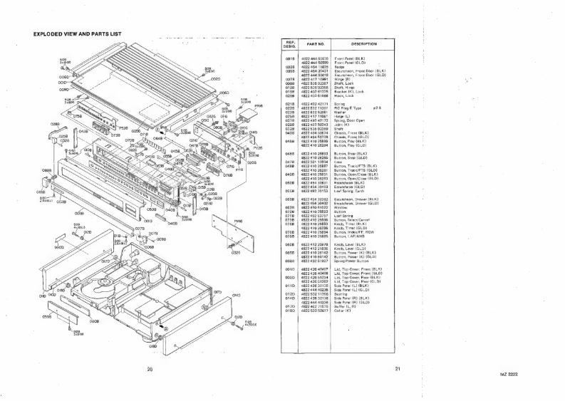
EXPLODED VIEW AND PARTS LIST
3x5) O14G
5128 4x30(U)
PART NO,
4822 444 50576 4822 444 50599 4822 454 11825 4822 454 30431 4822 444 50618 4822 417 t09g91 4822 535 92367 4822 536°92368 4822 402 61225 | 4822 402 61096
4822 492 42171 4822 532 11301 4822 632 52081 4822 417 11061 4822 492 42172 4822 402 50243 |. 4822 535 92369 4822 464 50674 4822 464 50709 4822 410 25889 4822 410 26284
4822 410 25893 4822 410 26285 4822 381 10904 4822 410 25887 4822 410 26281 4822 410 25891
4822 410 26283 4822 454 30831 4822 454 30403
4822 492 70153
4822 454 30382 4822 454 30402 4822 450 61022 4822 410 26892 4822 492 63757 4822 410 25886 4822 410 25883 4822 410 26286 4822 410 25884 4822 410 25885
4822 412 20979 4822 412 21006 4822 410 26142 4822 410 60142 4822 492 51927
4822 426 40407 4822 426 40408 4822 426 51234 4822 426 51262 4822 426 30135 4822 444 40235 4822 532 11266 4822 426 30136 4822 444 40236 4822 462 71578 4822 532 52077
; DESCRIPTIGN
Front Panel (BLK} Front Panel {GLD)
_ Badge re
Escutcheon, Front Door (BLK} Escutcheon, Front Door {GLD)
‘Hinge (R) . Shaft, Lock
Shaft, Hinge Bracket (K}, Lock Hook, Lock
Spring
RG Ring E Type $2.5 Washer
Hinge {L} Spring, Door Open
Joint (K) Shaft :
Chassis, Front (BLK) ; ! Chassis, Front {GLD) : Button, Play (BLK) Button, Play (GLD}
Button, Stop (BLK) Button, Stop (GLD)
Lens ‘S
Button, Track/FTS (BLK} Button, Track/FTS {GLD} Button, Open/Close (BLK) Button, Open/Clase (GLD}- Escutcheon {BLK} Escutcheon (GLD) Leaf Spring, Earth
Escutcheon, Drawer (BLK}
Escutcheon, Drawer (GLD} Window
Button
Leaf Spring Button, Select/Cancel Knob, Timer (BLK}
Knob, Timer {GLD) Button, Index/FF, REW
Button, LAP/AMS
Knob, Level (BLK) Knob, Level (GLD} Button, Power (K) (BLK) Button, Power {(K) (GLD}) Spring Power Button
Lid, Top Cover; Front (BLK}
Lid, Top Cover; Front (GL.D)- Lid, Top Cover; Rear (BLK) Lid, Top Cover; Rear {GLO} Side Panel (L) {BLK} Side Panei (L} {(GLD} Bushing
Side Panel (R) (BLK) Side Panel (R} (GLD) Buffer (L, R) Collar (K)
24 MZ 2222

MZ 2223
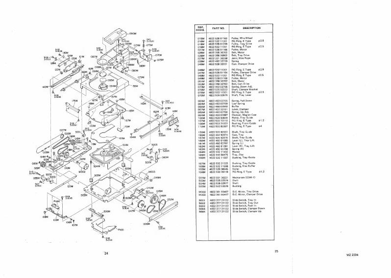
3x6(M}
22
003G 0456 047G 0606
061G O69G 2006 902G 905G 906G
A001
& FO01
43001 4091
4822 464 50493 Pistan, Dumper
4822 402 50237 Link, Power Switch
4822 256 91247 | Holder, Optical 4822 502 12511 B.T. Screw B3 x8 4822 462 41383 | Leg {BLK} 4822 462 41336 {| Leg {GLD} 4822 502 12511 B.T. Screw . B3 x8 4822 50111008 | 8.T. Screw : B4ax8 4822 325 20153 Support ,
4822 502 12511 B.T, Screw B3x8
4822 502 12571 B.T, Screw B3x8
4822 502 12611 | &.T. Screw 83x 8
4822 502 12511 B.T, Screw B3 x8
4822 691 30222 | Mechanism, Loading
4822 253 30014 Fuse T315mA [E} 4822 253 30127 | Fuse T250mA [N, A, T, WI -
4822 256 30233 Jack, Fuse Holder
4822 272 10227 | Voltage Selector [E]} 4822 272 10236 | Voltage Selector [N, A, T, W] 4822 267 30986 | Plug, AC Inlet ;
4822 146 30679 | Power Transformer [E] 4822 148 80772 Power Transformer [N, A, T, W}
4822 53560105 | Adaptor
23
5128 3x5(U)
5128 3x8(M)
hy
5128 3x8(M)
a
x
es (94M
193)
oem-*(@ i
OISM
SHO 2xl4(A)
035M
5110 2x5(A)
5I06 3x3 (A)
24
5128 3x8(M)
5128 2,6x4(U)
> 163M
141M
5128 ¥ 3x8(M)
5128 3x8(M)
4822 528 81163 4822 532 11301 4822 528 81238 4822 532 11301 4822 528 81166 4822 358 30762 4822 358 30903 4822 321 30338 4822 492 32719 4822 528 30331
4822 532 11301 4822 528 81164 4822 532 11301 4822 528 81166 4822 358 30762 4822 358 30763 4822 492 63706 4822 535 92332 4822 532 11301 4822 535 92575
4822 492 63705 4822 492 63709 4822 466 61549 4822 402 30161 4822 492 63706 4822 402 61097 4822 528 90645 4822 530 70119 4822 532 21323 4822 530 80307
4822 535 92331 4822 444 50574 4822 535 92576 4822 402 61089 4822 492 63707 4822 402 61091 4822 492 63708 4822 532 11432 4822 444 60475 4822 532 11697
4822 532 21323 4822 532 11698 4822 528 90645 4822 530 70119
4822 691 30221 4822 535 92574 4822 535 92577 4822 532 52076
4822 361 60467 4822 361 60447
4822 277 21132 4822 277 21132 4822 277 21132 4822 277 21132 4822 277 21132
ES PART NO. DESCRIPTION
Pulley, Wire Wheel
RG Ring, E Type $2.5
Pulley, Tray Drive
RG Ring, E Type o2.5
Pulley, Motor
Belt, Motor Belt, Tray Drive
Joint, Wire Rope
Spring Cam, Ciamper Drive
RG Ring, E Type $2.5
Pulley, Clamper Drive
RG Ring, E Type $2.5
Pulley, Motor
Belt, Motor Belt, Cam Drive
Spring, Down Adj.
Shaft, Clamper Bracket
RG Ring, E Type o2.5
Shaft, Tray Lever
Spring, Pull Down
Leaf Spring
Buffer
Lever, Clamper
Spring, Up Adj.
Clamper, Magnet Case
Roller, Tray Guide RG Ring, E Type $1.2
Bushing, Front Guide
RG Ring, E Type o4
Shaft, Tray Guide Case, Tray Shaft, Tray Guide
Lever (L), Tray Lift
Spring (L) Lever (R), Tray Lift Spring (R) Washer
Tray, Disc
Bushing, Tray Guide
Bushing, Tray Guide Bushing, Disc Buffer
Roller
RG Ring, E Type
Mechanism (CDM-1) Shaft
Shaft
Bushing
D.C. Motor, Tray Drive
D.C. Motor, Clamper Drive
Slide Switch, Tray In
Slide Switch, Tray Out
Slide Switch, Push In
Slide Switch, Clamper Down
Slide Switch, Clamper Up

ELECTRICAL PARTS LIST
ene PART NO. DESCRIPTION ASSIGNMENT OF COMMON PARTS CODES. RESISTOR ee PART NO. DESCRIPTION PART NO. DESCRIPTION
R***: (1) GDO5 --- 140, Carbon film fixed resistor, +5%, 1/4W Re: (2) GDOE --- 160, Carbon film fixed resistor, +5%, 1/6W
@— Resistance value PD16-DEMO PM16-RESISTORS C734 4822 121 51144 Film 1000pF +2%
CIRCUIT BOARD (All Resistors are +5% and 1/16W) C738 | 4822 12490387 | Elect 220uF 6.3V Examples 4822 111 90895 10KQ, Chip C739 | 4822 12490387 | Elect 220uF 6.3V
@ = Resistance value PD16-CAPACITORS 4822 111 90895 10KQ, Chip C740 4822 124 90352 Elect 10uF 16V
0.19,.,001 100...100 1kN...102 100kN...104 4822 124 22289 Elect 6.8uF 50V 4822 111 90895 10KQ, Chip C785 4822 124 22238 Elect 100uF 25V
0.59...005 189...180 2.7kQ...272 680kN...684 4822 122 40528 Ceramic 27pF +5% 4822 111 90895 10KQ, Chip C786 4822 124 22238 Elect 100uF 25V
19...010 1009...101 10k9...103 1MkQ...105 4822 122 40528 | Ceramic 27pF +5% 4822 111 90895 10KQ, Chip C787 4822 124 41535 Elect 100uF 25V 6.80...068 3900...391 22k...223 4.7Mk0Q...475 4822 121 42327 Film 470pF +5% 4822 111 90896 100KQ, Chip C788 4822 124 41535 Elect 100nF 25V
a 4822 121 42327 | Film A7T0pF 45% 4822 111 90896 100K 2, Chip C795 | 4822 12422238 | Elect 100uF 25V (Note) Please distinguish 1/4W from 1/6W by the shape of parts 4822 122 32486 Ceramic 0.01nF +80% —20% 4822 111 90894 1KQ, Chip C796 4822 124 22238 Elect 100uF 25V
used actually. 4822 12232486 | Ceramic 0.01uF +80% —20% 4822 11191414 102, Chip C797 | 4822 12441535 | Elect 100uF 25V 4822 111 90906 2.2KQ, Chip 4822 124 41535 | Elect 100 F
CE nO EAE PD16-SEMICONDUCTORS a ea ule ee 4822 130 80302 | Varistor MA27A 4822 11191414 102, Chip C803 | 482212232486 | Ceramic 0.01uF +80% —20%
O® Temp. coeff. P360 ~ N1000, 50V 4822 111 90894 1KQ, Chip c804 | 482212232486 | Ceramic 0.014F +80% —20% 4822 130 33305 | Diode 188176, etc. 4822 111 90918 4.7KQ, Chip C805 | 4822 12422735 | Elect 6800uF 27V
Capacity value 4822 111 90918 4.7KQ, Chip C806 | 4822 12422735 | Elect 6800uF 27V Tolerance 4822 130 33305 | Diode 188176, etc. 4822 111 90892 02, Chip C807 | 482212490058 | Elect 47 uF 25V
4822 116 60307 12 ’”W, Fusible C808 4822 124 90058 Elect. 47uF 25V
Examples ; at. 4822 209 71001 SAA7210 4822 111 91139 6.8KQ, Chip C811 | 4822 12422734 | Elect 470uF 25V @ __ Tolerance (Capacity deviation) 4822 209 73952 MB81416C-15 C812 | 4822 12422734 | Elect 470uF 25V oe 4822 209 72545 SAA7220P/B PM 16-SEMICONDUCTORS - C821 | 4822 12490364 | Elect 220uF 16V ee oe 4822 209 83641 1R2339 pre es ype Boe ren HtHY oe C831 | 482212232486 | Ceramic 0.01uF +80% —20%
2 SANTOR : 4822 13042591 | Transistor 2SA1175(FF, EF) iode , Chip (ORS er Hades sere here are as follows: 4822 130 61438 Tranesiar 2SA1005(K, L) 4822 130 32508 Diode RL103E, etc. C834 4822 122 32486 Goreme 0.01uF +80% —20%
oF ~ 1OpF 40. 5pF 4822 130 42591 Transistor 2SA1175(FF, EF) 4822 130 33948 | Zener 5.6V C836 4822 124 22723 | Elect 1000uF 25V
12pF ~ 560pF .. .+5% 5322 130 42052 | Transistor 2SC2785(FF, EF) C837 | 4822 124 22723 | Elect 1000uF 25V @ Capacity value 5322 13042052 | Transistor 2SC2785(FF, EF) 4822 130 80346 | Zener 02CZ8.2, Chip C838 | 4822 12490364 | Elect 220uF 16V
O.5pF...005 3pF...030 100pF...101 5322 130 42052 | Transistor 2SC2785(FF, EF) 4822 130 80346 | Zener 02CZ8.2, Chip C839 | 4822 12490364 | Elect 220uF 16V IpF...010 10pF...100 220pF...221 C841 | 482212232486 | Ceramic 0.01uF +80% —20%
1.5pF...015 47pF...470 560pF...561 4822 209 11497 MSM83C154 C845 | 4822 12422243 | Elect 6800uF 16V 4822 209 11496 | IC MSMB80C51 c846 | 4822 12490364 | Elect 220uF 16V
c***: CERAMIC CAP. it ; ; 4822 209 51273 | IC MSM2816/XL2816 Pa Drees eee aa AIP lech PeniAe Disce tani ue neer PD16-MISCELLANEOUS 4822 13061437 | Semicon Composit DTC114YK PP16-RESISTORS
Disc type 4822 130 61437 | Semicon Composit DTC114YK 1) Temp. chara. 2B4, 50V 4822 130 61437 4822 209 73949
Semicon Composit DTC114YK PST524D
4822 242 72395 | Crystal 11.2896MHz 4822 116 80262 2.37KQ 41% %W ee Capacity value
Example @® Capacity value
100pF...101 1000pF...102 10000pF...103 470pF ...471 2200pF..,222
C***; ELECTROLY CAP. ( 2 ), FILM CAP. ( 2 ) (1) EA------ 10, Electrolytic condenser
ag One-way lead type, Tolerance +20%
U—_ Dielectric strength Capacity value
Examples ea Capacity value CIRCUIT BOARD AR803 | 4822 116 60446 3.32 +5% %%W, Fusible
O.1nF...104 4.7uF...475 100uF...107 PM16-CAPACITOR A R804 | 4822 116 60446 3.32 +5% ‘%W, Fusible 0.33uF...334 10uF...106 330uF...337 4822 12232703 | Ceramic 330pF +10%, Chip PP16-CAPACITORS R807 | 5322 116 53214 5622 12% ‘WwW
TwF...105 22yF...226 1100uF...108 4822 122 33117 | Ceramic 330pF +5%, Chip 4822 122 40491 | Ceramic 0.022uF +80% —20% R808 | 5322 11653214 5622 42% YAW 2200uF ...228 4822 12232703 | Ceramic 330pF 10%, Chip R809 | 482211653079 | 3.83KQ 42% ‘%W
@ Working voltage 4822 122 32486 Ceramic O0.01uF +80% —20% R810 4822 116 53079 3.83K2 42% YW
6.3V...006 25V...025 4822 12232703 | Ceramic 330pF +10%, Chip R813 | 482211652956 | 1.21KQ 12% %W 10V...010 35V...035 16V...016 50V...050
4822 209 10306 4822 209 73951
4822 265 10062 4822 321 22588
4822 122 32703
PD26-OPTICAL OUT CIRCUIT BOARD
Ic TC4049BP Ic PST523D
Jack, 3P
Jack, Optical
PM16-FEATURE U-COM CIRCUIT BOARD
Ceramic 330pF +10%, Chip
4822 209 83803 4822 209 83803 4822 130 61437
4822 156 10676
4822 242 71781 4822 242 71781
4822 122 40617 4822 122 32486
LB1645N LB1645N
Semicon Composit DTC114YK
PM16-MISCELLANEOUS Choke Coil
Seramic Vibrator, 12.0MHz
Seramic Vibrator, 12.0MHz
PP16-AUDIO/POWER
Ceramic
Ceramic
47yF
0.1uF +80% —20% 0.01nF +80% —20%
4 R802
4822 116 80262
4822 116:60446
4822 116 60446
4822 116 60553 4822 116 60553
4822 116 52956
5322 116 53185
2.37K2
472
472
+5%
YW
YW
YW
AW
WwW iy BETS 2880, Gace ase a 4822 121 42691 | Film 2200pF ~ +5% R816 | 532211653185 | 1.47K2 412% %W
: = 4822 12151144 | Film 1000pF +2% R817 | 482211652956 | 1.21KQ +2% %W \__ Capacity value 4822 122 32703 | Ceramic 330pF +10%, Chip 4822 121 42691 | Film 2200pF 15% R818 | 482211652956 | 1.21KQ 12% WwW
4822 12151144 | Film 1000pF 12% R871 | 4822 116 60331 1KQ 15% 1W Examples 4822 124 90387 | Elect 220uF 6.3V 4822 116:60331 1W
@ Capacity value 4822 122 32703 | Ceramic 330pF +10%, Chip 4822 124 90387 | Elect 220uF 6.3V 0.001 uF (1000pF). ..102 0.1 uF... 104 4822 124 90352 | Elect 10uF 16V
O.0018uF 2.2... 1820 O.56yF...564 4822 12232703 | Ceramic 330pF +10%, Chip 4822 121 42691 | Film 2200pF 15% O.01uF............. 103 TyF...105 4822 12151144 | Film 1000pF +2%
0.015uF......... 153 4822 121 42691 | Film 2200pF 15%
MZ 2225
26
YW, Fusible
YW, Fusible

DNO8 DNOg DN10 DN11
D806 A D807 A D808 4 D809 4 D810
D821 D822 D823
A D833 A D834 4 D841 AD842 AD843
QNO1 QNO2
Q702 Q703
4Q801 Q802 Q803
4 0804 Q805 Q806
40821
AF831 A F832
JD20
JGO3 JG11 JG12 JG13
4822 130 31018
4822 130 31018 4822 130 31018 4822 130 31018 4822 130 32377 4822 130 32377 4822 130 31018
4822 130 32366 4822 130 32366 4822 130 32155 4822 130 32155 4822 130 32155 4822 130 32155 4822 130 32191 4822 130 80425 4822 130 31018 4822 130 32508
4822 130 32508 4822 130 32508 4822 130 32508 4822 130 33056 4822 130 33056 4822 130 33056 4822 130 33056
4822 130 42591 4822 130 61439 4822 130 42052
4822 209 73953 4822 209 73953 4822 209 70226 4822 209 70226
4822 130 43311 4822 130 60839 4822 130 60107 4822 130 43023 5322 130 42052 4822 130 42591 4822 130 61176 4822 130 42591
4822 253 30018 4822 253 30018 4822 253 30024
4822 265 10062 4822 265 20354
4822 256 30329 4822 267 30978 4822 256 30329 4822 267 30978 4822 256 30329 4822 267 30978
4822 267 31027
4822 142 60388 4822 280 20361
PART NO. DESCRIPTION
PP16-SEMICONDUCTORS
Diode 188155, etc.”
Diode 188155, etc.
Diode 188155, etc.
Diode 1SS155, etc.
Zener RD3.9EB1
Zener RD3.9EB1
Diode 18S155, etc.
Zener 5.6V
Zener 5.6V
Diode WO6B
Diode WO6B Diode WO6B
Diode WO6B
Zener RD7.5E-B3
Zener 4.7V
Diode 18S8155, etc.
Diode RL103E, etc.
Diode RL103E, etc. Diode RL103E, etc. Diode RL103E, etc.
Diode U05B
Diode U05B
Diode U05B Diode U05B
Transistor 2SA1175(FF, EF) Transistor 2SB1237(R) Transistor 2SC2785(FF, EF)
NJM4580DD Ic NJM4580DD Ic NJM5534D Ic NJM5534D
Transistor 2SC3298(O, Y) Transistor 2SC2458(Y, GR)
Transistor 2SA1048(Y, GR) Transistor 2SA1306(O, Y) Transistor 2SC2785(FF, EF) Transistor 2SA1175(FF, EF)
Transistor 2SB1357(D, E)
Transistor 2SA1175(FF, EF)
PP16-MISCELLANEOUS Fuse T630MA
Fuse T630mMA
Fuse T1.6A
Jack, 3P Terminal, 1P; RCA
Jack, Fuse Holder
Jack, Fuse Holder
Jack, Fuse Holder
Jack, Fuse Hoider
Jack, Fuse Holder
Jack, Fuse Holder
Terminal, Audio Out
Pulse Transformer
Relay
aera PART NO. DESCRIPTION
PP26-DAC CIRCUIT BOARD
PP26-CAPACITORS 4822 122 40617 Ceramic O.1uF +80% —20%
4822 124 22238 Elect 100uF 25V
4822 122 40617 Ceramic O.1uF +80% —20%
4822 124 22238 | Elect 100uF 25V 4822 122 40617 Ceramic O.1yF +80% —20%
4822 122 40617 Ceramic O.1uF +80% —20%
4822 122 40617 | Ceramic O.1uF +80% -20% 4822 124 90058 | Elect 47 pF 25V 4822 122 40617 Ceramic O.1uF +80% —20%
4822 124 90058 Elect 47 uF 25V
15% 15%
4822 121 42713 4822 121 42713
Film
Film
680pF 680pF
4822 121 43268 Film O.1uF +10%
+10% 4822 121 43268 Film 0.14F
4822 124 22237 4822 124 22237
10uF
10uF Elect Elect 16V
4822 124 22237 | Elect 10uF C664 4822 124 22237 | Elect 10uF 16V C671 4822 121 51282 | Film 2400pF +2% C672 4822 121 43271 Film 5600pF 15% C673 4822 121 43269 | Film 0.018uF +5% C674 4822 121 54282 | Film 2400pF +2% C675 4822 121 43271 Film 5600pF 15% C676 4822 121 43269 | Film 0.018uF 15% C681 4822 12151282 | Film 2400pF +2% C682 4822 121 43271 Film 5600pF +5%
4822 121 43269 | Film 0.018uF C684 4822 121 51282 | Film 2400pF +2% C685 4822 121 43271 Film 5600pF +5% C686 4822 121 43269 |. Film 0.018uF +5% C691 4822 124 22238 | Elect 100yuF 25V C692 4822 124 22238 | Elect 100uF 25V C693 4822 124 22238 | Elect 100uF 25V C694 4822 124 22238 | Elect 100uF 25V
PP26-RESISTORS R631 4822 116 53758 1.62KQ +2% *”W R632 | 4822 116 53393 8252 +2% YAW R636 | 4822 116 53758 1.62KQ +2% ww R637 | 4822 116 53393 8252 +2% ”~W R641 4822 116 53758 1.62KQ2 £2% %W R642 | 4822 116 53393 8252 42% “~W R646 | 4822 116 53758 1.62KQ +2% ”~W R647 4822 116 53393 8252 +2% ~W
A R691 4822 116 60446 3.3Q +5% YW A R692 | 4822 116 60446 3.32 +5% *~W A R693 | 4822 116 60446 3.32 +5% *W A R694 | 4822 116 60446 3.32 +5% ”~W
PP26-SEMICONDUCTORS Q601 4822 209 72969 | IC TDA1541A Q602 | 4822 209 72969 | IC TCA1541A Q603 4822 209 73953 | IC NJM4580DD Q604 | 4822 209 73953 | IC NJM4580DD Q607 | 4822 130 42842 | F.E.T 2SK372(GR, BL) Q608 | 4822 130 42842 | F.E.T 2SK372(GR, BL) Q609 | 4822 130 42842 | F.E.T 2SK372(GR, BL) Q610 | 4822 130 42842 | F.E.T 2SK372(GR, BL)
28 MZ 2226

PART NO. DESCRIPTION PART NO. DESCRIPTION
PP36-3 REGULATOR CIRCUIT BOARD
PV 16-SEMICONDUCTORS 4822 130 33305 | Diode 188176, etc. 4822 130 32191 Zener RD7.5EB3 4822 130 33305 | Diode 18S176, etc. 4822 130 33305 | Diode 188176, etc. 4822 130 33305 Diode 188176, etc. 4822 130 33305 Diode 188176, etc.
Diode 4822 130 32508 RL103E, etc.
Ic NJM7912FA
Ic NJM7812FA
Transistor 2SD1913(R, S)
4822 209 73954 4822 209 70084 4822 130 61442
4822 130 32366 Zener 5.6V
4822 209 80401 Ic NJM4558D
4822 130 42591 Transistor 2SA1175(FF, EF)
5322 130 42052 | Transistor 2SC2785(FF, EF) 4822 13061179 | Transistor 2SD2037(D, E)
4822 13061176 | Transistor 2SB1357(D, E) 4822 13061176 | Transistor 2SB1357(D, E)
4822 13061179 | Transistor 2SD2037(D, E) 4822 209 83643 Ic 1R3741
4822 209 80401 Ic NJM4558D
4822 130 42591 Transistor 2SA1175(FF, EF)
PR16-HEADPHONE AMP CIRCUIT BOARD
4822 100 20632 Variable Resistor 10K 9(A)
Ic NJM4556D
Transistor 2SC2878
Transistor |2SC2878
Transistor 2SC2878
Transistor 2SC2878
4822 209 83654
Q903 4822 130 43818 Q804 | 4822 130 43818 Q905 4822 130 43818
4822 130 43818
4822 267 31026 Jack, Headphone 5322 130 42052 Transistor 2SC2785(FF, EF) °
4822 130 42591 Transistor 2SA1175(FF, EF)
5322 130 42052 Transistor 2SC2785(FF, EF)
5322 130 42052 Transistor 2SC2785(FF, EF) 4822 209 71674 | IC 80C51 5322 130 42052 | Transistor 2SC2785(FF, EF)
PS16-LINE FILTER/POWER SWITCH CIRCUIT BOARD
CHO1 4822 123 30064 Film Cap. 0.15uF +20% [A,N,E]
CHO2 4822 123 30064 Film Cap. 0.154F +20% [A,N,E]
CHO3 4822 123 40488 Ceramic Cap. 470pF +10% [A,N,E]} 4822 123 40488 Ceramic Cap. 470pF +10% [A,N,E]
4822 209 80401 IC NJM4558D 4822 130 42591 Transistor 2SA1175(FF, EF) 4822 130 42591 Transistor 2SA1175(FF, EF)
4822 130 42842 | F.E.T. 2SK372(GR, BL) 4822 130 42842 | F.E.T. 2SK372(GR, BL) 4822 130 61441 Transistor 2SD1862(Q, R)
4822 122 33276 Ceramic Cap. 0.01nF +20%
4822 116 80472 Resistor 220K2 +10% “WIA,N,E] PV16-MISCELLANEOUS
4822 157 53801 Choke Coil 47uH 4822 157 53801 Choke Coil 47uH
4822 276 11141 Push Switch, Power
PS26-TEN KEYS CIRCUIT BOARD
4822 242 71781 Ceramic Viblator 12MHz
PV26-SERVO MODULE CIRCUIT BOARD 4822 276 12455 | Push Switch, Tact
PV26-CAPACITORS 4822 121 43267 Film 6800pF +2% 4822 121 43267 Film 6800pF +2% 4822 121 43265 Film 5600pF 22% 4822 121 43265 | Film 5600pF +2%
4822 122 33084 | Ceramic 390pF 145% 4822 121 43266 Film 680pF 742%
4822 277 30883 Slide Switch
PV16-SERVO CIRCUIT BOARD
PV16-CAPACITORS C233 4822 124 21903 Elect 1uF 50V 4822 121 43264 Film 1800pF +2% C255 4822 124 21903 Elect Tur 50V 4822 121 43267 Film 6800pF +2% C257 4822 124 40464 Elect 4.7nF “BBV 4822 121 43267 Film 6800pF +2% C274 4822 124 90365 Elect 220uF 25V 4822 121 43267 Film 6800pF +2% C276 4822 124 90365 Elect 220uF 25V 4822 122 32904 | Ceramic O.1uF +10%, Chip
4822 124 90365 Elect 220uF 25V PV26-RESISTORS
{All Resistors are +5% and 1/10W) 4822 111 90883 10KQ £1%, Chip
4822 111 90883 10KQ +1%, Chip
4822 111 90885 2.7KQ £1%, Chip
4822 111 91365 4702 +1%, Chip
4822 111 90906 2.2KQ, Chip
4822 111 90883 10KQ +1%, Chip
4822 111 90883 10KQ +1%, Chip
4822 111 90885 2.7KQ £1%, Chip
4822 111 91365 4702 £1%, Chip
4822 111 90906 2.2K 2, Chip
PV16-RESISTORS
R211 4822 116 80256 5.62M2 +1% 1/6W R212 4822 116 80256 5.62MQ +1%° = 1/6W
AR231 4822 116 60314 102 15% ’W, Fusible AR232 4822 116 60314 102 +5% ’W, Fusible 4AR233 4822 116 53696 1202 +5% AW, Fusible AR234 4822 116 53696 1202 £5% “AW, Fusible R254 4822 116 80261 91KQ +5% 1/6W R274 4822 116 80252 13KQ +1% 1/6W R275 4822 116 80261 90.9KQ +1% 1/6W R277 4822 116 80255 357KQ +1% 1/6W
29
MZ 2227

sons PART NO. DESCRIPTION hens PART NO. DESCRIPTION hone PART NO. DESCRIPTION
4822 111 90895 10KQ, Chip R379 | 4822 111 90911 27KQ, Chip PY16-RESISTORS
4822 111 90895 10K 2, Chip R380 | 4822 111 90918 4.7KQ, Chip 4822 111 90925 68KQ, Chip R381 | 4822 111 90925 68KQ, Chip 4822 111 90901 150KQ. +5% = 1/10W, Chip
R314 | 482211190919 47KQ, Chip R382 | 4822 111 90918 4.7KQ, Chip R315 | 4822111 90919 47KQ, Chip R385 | 4822 11191359 27KQ +1%, Chip R316 | 482211190918 4.7KQ, Chip R386 | 4822 111 91357 180KQ +1%, Chip 4822 111 90895 10KQ 45% 1/10W, Chip
R317 | 482211190919 47KQ, Chip R387 | 4822 111 90919 47KQ, Chip R318 | 4822 111 90925 68KQ, Chip R388 | 4822 111 90919 47KQ, Chip 4822 111 90922 5.6KQ +5% = 1/10W, Chip
R320 | 4822 11191366 5.6KQ +£1%, Chip R389 | 4822 111 90896 100KQ, Chip 4822 111 90922 5.6KQ 15% —1/10W, Chip
4822 111 91355 13KQ +1%, Chip R390 | 4822 111 91367 75KQ +1%, Chip 4822 111 90922 5.6KQ +5% — 1/10W, Chip 4822 111 91139 6.8KQ 45% 1/10W, Chip
R323 4822 111 91361 330KQ +1%, Chip R324 | 4822111 90916 3.9KQ, Chip R325 | 4822 111 91369 1.5KQ, Chip
R391 4822 111 91367 T5KQ +1%, Chip R393 | 4822 111 91361 330KQ +1%, Chip R394 | 4822 111 90908 220KQ, Chip
4822 111 90922 4822 111 90922
5.6K2 +5% 1/10W, Chip 5.6KQ +5% 1/10W, Chip
R326 | 4822 111 90907 22KQ, Chip R395 | 4822 111 90896 100KQ,, Chip 4822 111 90918 4.7KQ, 5% = 1/10W, Chip R327 | 4822111 90907 22KQ, Chip R396 | 4822 111 91368 120KQ, Chip 4822 111 90918 4.7KQ +5% 1/10W, Chip
R328 | 4822111 90923 56KQ, Chip R397 | 4822 111 90919 47KQ, Chip 4822 111 90918 4.7KQ +5% 1/10W, Chip
R329 | 4822111 90923 56KQ, Chip R398 | 4822 111 90919 47KQ, Chip 4822 111 90914 330K2 +5% 1/10W, Chip
R330 | 482211191192 4700, Chip 4822 111 90895 10KQ 45% 1/10W, Chip ,
R331 | 482211191192 4702, Chip PV26-SEMICONDUCTORS 4822 111 90895 10KQ 45% 1/10W, Chip
4822 111 91372 8202, Chip 0301 | 4822 130 80274 | Zener 2.4V, Chip D302 | 4822 130 43408 | Diode MA151WK, Chip PY 16-SEMICONDUCTORS
4822 111 91369 1.5KQ, Chip D303 | 4822 130 43408 | Diode MA151WK, Chip R334 | 482211191192 4702, Chip D304 | 4822 13032868 | Diode MA 153, Chip 4822 130 32635 | Diode MA151K, Chip R335 | 4822111 91373 82KQ, Chip D305 | 4822 13032955 | Zener 5.1V, Chip R336 | 4822 111 90925 68KQ, Chip 4822 130 32635 | Diode MA151K, Chip
4822 209 71677 R337 | 4822 111 91356 130KQ £1%, Chip Ic LC6554D
R338 | 4822 111 90923 56KQ, Chip R339 | 4822111 90907 22KQ, Chip
4822 209 71675 NJM2902M Q302 4822 209 71675 IC NJM2902M 4822 130 61436 | Semicon Composit DTA114YK
R340 | 4822 111 90896 100KQ, Chip 0303 | 4822 20971675 | IC NJM2902M
R341 4822 111 91371 470KQ, Chip Q304 | 4822 20971676 | IC NJM2901M 4822 130 42737 | Transistor 2SD1328(S), Chip
4822 111 90895 10KQ, Chip Q305 | 4822 20911607 | IC 4030 4822 130 42737 | Transistor 2S8D1328{S), Chip
Q306 | 4822 209 83368 | IC 4053 4822 130 43398 | Transistor 2SC2712(G), Chip
4822 111 90918 4.7KQ, Chip Q307 | 4822 209 71451 Ic NJM4558M 4822 130 43398 | Transistor 2SC2712(G), Chip
R345 | 4822111 90918 4.7KQ, Chip Q308 | 4822 13060658 | Transistor 2SC2351, Chip 4822 130 43398 | Transistor 2SC2712(G), Chip
R346 | 482211191371 470KQ., Chip Q309 | 4822 209 83363 | IC FMW1 4822 209 73951 Ic PST523D
R347 | 4822 111 90896 100KQ, Chip 4822 209 83363 | IC FMW1
R348 | 4822111 90913 33KQ, Chip R349 | 4822111 90926 8.2KQ,, Chip R351 4822 111 90926 8.2KQ, Chip R352 | 4822111 90925 68KQ, Chip R355 | 4822 111 90923 S56KQ, Chip
4822 111 91358 24KQ2 +1%, Chip
PY 16-MISCELLANEOUS
4822 276 11559 | Push Switch, Stop 4822 276 11559 | Push Switch, Pause
4822 276 11559 Push Switch, Play
Q312 4822 130 42733 | Transistor 2SA1162(G), Chip Q314 4822 130 60146 Semicon Composit DTC144EK
Q315 4822 130 43398 | Transistor 2SC2712(G), Chip
Q316 4822 130 60657 | Transistor 2SC1009, Chip
Q317 4822 13060657 | Transistor 2SC1009, Chip Q318 4822 130 60146 Semicon Composit DTC144EK
4822 276 11559 | Push Switch
4822 111 90897 IMQ, Chip R358 | 4822111 91363 360KQ 41%, Chip R359 ) 4822 111 90907 22KQ, Chip R360 | 4822 111 90887 6.8KQ +1%, Chip R361 4822 111 90887 6.8KQ +1%, Chip
4822 130 90441 Display Unit
PV36-PHOTO REFLECTOR CIRCUIT BOARD 4822 242 71495
4822 130 81183 Ceramic Vibrator 3.00MHz
Photo Unit
R362 4822 111 90889 82K +1%, Chip 4822 130 81182 L.E.D. ON2179R
R363 4822 111 90889 82KQ +1%, Chip
R364 | 4822111 90918 4.7KQ, Chip PY26-LAMP CIRCUIT BOARD
R365 4822 111 90895 10KQ, Chip PY16-DISPLAY CIRCUIT BOARD 4822 130 32508 | Diode RL103E, etc. 4822 130 32508 | Diode RL103E, etc.
4822 111 91371 470KQ, Chip PY 16-CAPACITORS
CcY02 4822 122 32669 Ceramic 0.047pF, Chip
cY04 4822 122 32693 Ceramic 33pF +5%, Chip
4822 122 32693 Ceramic 33pF +5%, Chip
4822 111 90913 33KQ, Chip R368 | 4822111 90895 10KQ, Chip R369 | 4822111 90918 4.7KQ, Chip R370 | 4822111 91362 386KQ £1%, Chip R371 4822 111 91346 3.9KQ £1%, Chip R372 | 4822 111 91363° 360KQ +1%, Chip R373 4822 111 90909 2.7KQ, Chip R374 | 4822111 90896 100KQ, Chip R375 | 4822111 90918 4.7KQ, Chip
4822 111 90913 33KQ, Chip
4822 134 40865 Lamp, Play
4822 134 40864 Lamp, Pause
4822 122 32697 Ceramic 2200pF +10%, Chip
NOTE ON SAFETY: Symbol! A Fire or electrical shock hazard. Only origina! parts should
be used to replace any part marked with symbol A . Any other com-
ponent substitution {other than original type), may increase risk of
fire or electrical shock hazard.
30 31
MZ 2228

BLOCK DIAGRAM
melo DIG. OUT
AC INLET vo cated eames md 208 A.soss 2 i SELECTOR On o>
1
OF G ws PPI6 AUDIO/ POWER P.W.B O 1 a 06 6 TRANSFORMER o! aA Jolt ee
0 JHO! ae] 1 1 1
an PSI6 : O to} 10
> a O oO O s iB! Ig OAS toils
6 ne oO O O
ie pa aac We) sree E 7 [Ee OO O1] - res
acsse TT =-]3 a Bo {e) Bo O71] wos LOO O Ol Jweo3 POWER SW im
WFO6 ‘ 4
faces GRY
(oS eos. [ 7
w iva]
3302] 3206 i paleo PP26
ceo ©=DAC RW.B
PV26
DEMO/ERCO DIGTAL FILTER
SERVO MODULE PVIG PW.B. SERVO P.W.B.
PDI6 | DEMO/ERCO
J202 | PW.B.
EER TG Se erent my | | 2 | CoC =e rumeer ee cme
° U a re) > | O° c oes | 0 = @ TRY DRIVE
CLAMPER DRIVE
PYI6 vvo2 |
DISPLAY PW.B. DOWN END SW.
$004 DOWN END
Vee
TRAY MOTOR OUT
TRAY MOTOR IN
CLMPER MOTOR DOWN
CLMPER MOTOR UP
N_END Sw. PEND FTS COM
FEATURE COM
, 66 | ! D ©) @ PMs =
FEATURE » COM PY 26 PW.B. | LAMP PW.B. |
MZ 2229
PP36 REG P.W.B.
uso3 b waos ws0o3 REGU
won TOO LETT aIwsi0 WwDOi
PRI6 HEADPHONE JACK P.W.B.
HEADPHONE OUT.
PS26 TEN KEYS PW.B.

AC
WIRING DIAGRAM
INLET SS BRN
Joss [Sey
BLU
PS1I6 POWER SW.
P.W.B.
POWER SWITCH
PP26 DAC. P.W.B. PP36 BEG. PW. 2
BRN on BLU
BLK RED BRN RED
ORG
FUSE FOOI veL__ ASN VOLTAGE > Ai : <\ FUSE FOO! VOLTAGE SS G09 SELECTOR AC INLET EW) AEN sevector
es WEF Jos JO93 9) a Jog! FUSE HOLDER = FUSE HOLDER Jool ao a JOO! BLU
GRN BRN
BLU
POWER POWER TRANSFORMER TRANSFORMER
J010
PSI6 @) POWER SW.
TO PMI6 (UFIO) PW.B.
YEt
=’] ® YEL
WHT. SK TO PMI6 (JFIO)
TO PPI6 (J80l)
(A,N,T,W) VERSION POWER SWITCH
Ns Tega JB02 teal sania ASSAD io Tercera contenant
HEMMER MN ENICRU ERE TRAY DRIVE CLAMPER DRIVE MOTOR MOTOR ee moo! moo2 UP END SW. IN END SW. IN SENSOR SW. OUT END SW. DOWN END Sw.
(IN/OUT) (UP/ DOWN) $005 soo! $003 $002 $004
FL J PMI6 FEATURE » COM P.W.B.
TO PMI6 (JFO3)
CDM - | ©)
TO PVI6 (3203)
PYI6 DISPLAY P.W.B.
T.T. MOTOR Sa
ff,
PRI6 HEADPHONE JAC
PY26 LAMP PW.B.
PS TE
LEVEL PHONES

PD26 OPTICAL OUT P.W.B.
PP26 DAC. P.W.B. PP36 REG PW.B.
Pee ee
AG A BLU
BRN RED
jc FUSE FOO! FAN VOLTAGE = Ay) ob SELECTOR
S) Jog! PPI6 OUTPUT DIG OUT PDIG a FUSE HOLDER za DAC/ POWER PWB. DEMO / ERCO PW.B. BRN — Smet gee p
POWER TRANSFORMER
JO10
PSI6 YEL
NER SW. a’) @) W.B. cli TO PMI6 (JFIO)
BLK
wDOi
Jott
(A,N,T,W) VERSION WER SWITCH
ws02 WSO T END SW. DOWN END Sw.
; wsitt 002 $004
3 J PMI6 FEATURE COM PW.B.
PV26 SERVO MODULE PW.B.
PRIG HEADPHONE JACK
PY26 LAMP PW.B.
PS26 TEN KEYS PW.B.
LEVEL PHONES
MZ 2230

MZ 2231
PARTS LOCATION (Pattern Side)
“SERVICE INFORMATION IS FOR USE BY QUALIFIED PERSON- NEL ONLY — ANY MISADJUSTMENT OR MISALIGNMENT MAY BE TREATED AS ANON-WARRANTY REPAIR BY ANY MARANTZ SERVICE CENTRE
Kind of Common Parts
RESISTOR
R*** (1) GDOS .... 140, Carbon film fixed resistor, +5% 1/4W
R*** (2) GDOS5 .... 160, Carbon film fixed resistor, +5% 1/6W
Cc*** : CERAMIC CAP.
(1) DD1 ..... 370, Ceramic condenser,
disc type (titan condenser)
Temp. coeff. P350 to N1000 50V
C*** : CERAMIC CAP.
(1) DK16 .... 300, High dielectric constant ceramic condenser, disc type (titan variable) Temp. chara. 2B4 50V
CG : ELECTROLY CAP. ( 22 )/FILM CAP. (=) (1) EA isc ses 10, Electrolytic condenser,
one-way lead type, tolerance +20% (2) DF15 .... 350, Plastic film condenser,
one-way type, Mylar, +5% 50V
* In case of ordering the common parts, please establish the correct parts number of 10 figures by the procedure “ASSIGNMENT OF COMMON PARTS CODES”
Components and wiring are subject to change for modification without notice.
NOTE ON SAFETY:
Symbol A Fire or electrical shock hazard. Only original parts
should be used to replace any part marked with symbol A. Any
other component substitution (other than original type), may
increase risk of fire or electrical shock hazard.
PS26 DISPLAY P.W.B.
(KC) |QF10
&
34
PYI6 DISPLAY PW.B.
QFO6 ~ QFO8
QYI2 ~ OYI4

PYI6 DISPLAY PW.B. _—-
PLAY P.W.B.
QYI2 ~ QYI4
QFO6 ~ QFO8 QFIO0
FT
34

SCHEMATIC DIAGRAM
\ TO PVI6 (J202)
PYIG DISPLAY PMI6 FEATURE ys COM P.W.B. PW.B. ah
=20V. | Ba
&
: PS26 TEN KEYS PW.B. 15 ssi4
OPEN/CLOSE RECALL ci 9° 9
} ssié
‘ ue re H 5B 0 ‘SSI0
ro)
i oO
: Ssol I
(|
CFaS 330p
why S085 0 9 0
2 8807.0 S902 7, En ro) °
3 cy | i SSOR A, SSOBR
Lyne 4 ‘9 ‘$80!
S898 a > Oo
$8i2 $313 Sa memgS cancen {JOIO)
ssi SELECT
TO TRAY SW.
|
& DY52
PY26 LAMP PW.B. a
35

Model CD-94MK2
TO PVI6 (J202) 77) brid. 7
c ae —— ge GOSS 0 NY Qyor avis ie ©)
— PMI6 FEATURE p COM P.W.B. 5 Lcess4D PST523D +12v
2SD1328(S) 28C2712(6) QY02~0Y06 OF
DTAN4aYK PST5240
QYIO,QYII
2SD1328(S) DTCH4YK DTAI4YK
Qvi2~oyl4 € C
28¢271216) 8 . E E
QMO! ,QMO02 21
LBI645N
QFOI
MSM80C59. Biase Biss 88°) ovoe
OFO2
MSMB8OC51 MSMBOC59 MSMB8OC5]
QFO3
MSM28I6A, XL2816A
1oviev
QFO7,QF08,QFI0,QMO3
DFO3, DFO5 MSM2BI6A
MAISIWK XL2BI6A
DYOI~ DYO6
MAISIK
DY5!,DY52, DF50,DF53 fe ee oe ot foa {pvos
y) . DMO1,DMO2
z 02¢28.2 § 3 3 g
4 F toviev 0.047 2 8h as g a ian OFSI 1 LBIG45N
Sao wf -TM e ing) : BL ey aT] é
5.6V ZENER
—<T
| 8] ai) 8) 8) s] 8] §]. 2 y = Qi cy oy SE 2
lei Ele Efe 20] 2) Pel Ge) £8
LS TO A a {) =
| oe
| | k k Dvst ‘Ni
Sp 6) TO TRAY Sw. c<s o~ fi k SEV, CENER pys2
ee Oo} vec | B |
RLIOSE MAISIK o2cze.2 GND out PY26 LAMP PW.B.
k DSFIOC MAISIWK 020768 PSTS230 PST524D
35
(MZ 2232

MZ:2233
PVI6 SERVO P.W.B. POI6 DEMO/ERCO P.W.B.
36
A
D30!,D305 D:
PV26 SERVO
MODULE P.W.B.

: | r i
“este
PDI6 DEMO/ERCO P.W.B.
36
0301,D305
PV26 SERVO
MODULE P.W.B.
K Al,A2 Q
O O
KI K2 D306 D304
Q308,Q315~Q318
PV36 PHOTO REF P.W.B.
KI, K2
O o Al A2
0302, D303
BI
Q309, Q3il
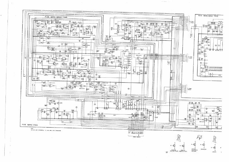
PV26_ SERVO MODULE P.WB.
tr
+5v a
ae, te Boe Bie Lez Lowe, R317 AT 12%) | 2%)
23 Q303T374 R390 | R391
@ 75k | 75k
ed
€307 0,033 R397 47k
€ R393 330k €310 680p
O%? hes
fA} 10. ff r
enon tae | Cebassie R366_470K
Q303(2/4) pseo sez 100k ark
Av} C3it 1800p
fs| Rae
| rn | Lf —fAK}—
Lo
[Li R365 (0K & IRse2
laze ~ ey. #12V “|
[ig ]osor R360 68k I
indoo’ Q301 ( 4%
1208 O-O 7535; -2 | | -2
Raiz tox
Q307(1/2)
REI
va0e-1 0 ie
| R34 470k is
| oy & R340_(00k Hoy PAM
1%) (2%)
eT PA}
S800p}
€302 6800p (2%)
Q304 (4/4)
R328 96k
eI R349 e.2k
NOTE
(961),(%2),083) 2 NECESSARILY To USE SAME TYPE TRANSISTOR
~l2v.
wao2-!
care 0047
DEMO/ERCO PW.B. vot
OF ve
1or RAD + S17 RAD -
sist Foc + €820 470p Lot Foc” |70 CDM-1 a i} FE (P100) 22k 6821 470p. © L
to! REZ JS5OL CBI RsI9 820, Re2e = ]
10 Oj REI folar 0.022 “22k ) (DP rer “8 im Bs ey
R385 27%
TOr—— sno q oe Q53! PDa ~i2v Cy Oo +12v
27 RB3O. $010k ces
ooze
=8 TY ERT ac
o = DS30
e 280 -RaeS ot 18k
[joe ee 47k
ae Sol few
1205-12, RT ST nce O) tae ene) Cb mee é ee
OHO 9301-12
3301-3 +5.
pay B88! eax B Sasso ry y 4
G9) @——@)--G!
c3t3 R382 a is E Lg es R387 1M ty
TAT swag /SEM vA oc!
0.022 4.7% cd rere Aw} Q306 i =
~6y. J30I-5 J205-5 weoz <8 [201-9 5208-8
ZS a Q304 (2/4) 1208-6 > aa TO PPI6 301-7 J208~7
(J802) s30i-6 1208-8 o = av. J30I- 4 205-4 o Fiey. —$)-O——
oO +ITV | | +O stop
| | |
——— te
1202)
afl +TV
10! +lav
SL a 1OF TO PMI6 ene °
rO,-— sno | (w202) oO {|
tei TXD Blssr” ososy | 4
Not ges. id
H4 R351 ae Bek
LL EE ree
C258 Reve R296 CBee O47 “220x 1k = G.22
R238 404 Bary Q: a406 hp 100%. . ct) raze me)
R259 254 C252 R255 Iw Razr Foor Gar Ges ‘47k R426 Be
R427 wok ary rem Q403
ry C2 C23 Q405 R254 Ress Ww 6800p Stk
s Lee z 330k 2: 2 O-~6 O O
Q251 (1/2) Ras} 100k
R423.
ane 4
+2V lav GND HFS. BS tRT ODA ORA och
WAB/ SSM
MSC NUsB a¥s6. ANIN
PDI6 (W201)
37
ae 3 ¢ ¢
B B
E 2SC2785 2SAiI75
282785 (FF,EF) 2SAil75 (FF, EF)
c c
8 B s
E E S a 28¢2351 2SA1162(6) 28C2712 (6) D 28C1009
28K372 oy

PDIG6 DEMO/ERCO P.W.B.
tev
€520 470p
c821 470p
ia vC+
Jot ve - 10; RAD +
tot RAD —
TO) roe - [TO CDM-1 tol re (P100)
R203 R210 Ti L a808 © RE2 023! 100k 100k Ded fel flue
na ~6v | |
CH 1Of 6ND d o-& TOF —t2v [ta
Roy R231 O +iev
y a 6) 38
0232 of °o e
c280 R263
or 18k
Sel le v208~12 sf ey [4208-8
Giessen ens erro O si ieee es auras ee J 301-12 3301-3
aA he! Bak ca R388 Na i ad 7} itt 48
ry . a] hs 3. Hepa
Eh so Bae Z f pees ee wns or 4/4) EET x px
304 (2/4) Of— SN? ito PPG 302 amen o -iav | (802)
6600p(2 %) (3/4) Rare B 9 ae?
O- 0-H ob eis A osoe[¥] b |
E+: rea bv.
By RBS oe
I | 27k 4 (4)22.
ral
R338 56k
202
0411/4) & af) sav © +12v
+01 +oV
{07 — *x© | TO PMIG € ° sno} (W202)
Lo! TxD
10; gusy
1} RES
J302-6 3302-5 9302-16 302-15
2
| | +5V_
lo2za]
INT/TL Ag ROIR
Q27i
| J206-15
4.7%[ “ Juz06-i6 R278
R278] R276 9O.9K BOK
C53! BO! usu
630 | Dl sto
TS
Cis R298 R296 526 O47 “220k tok 0.22
DACS DAC2 DACI DACO L Feo f BUSY RP ru J Fez
RESET TxD
Teee Re88 O66 47k
Q402 {2/2) alo RAOS
Rat ‘33k 220 a ® oO R413:
@—© 220 R406
R262 ‘580
Q25)
=@ Ox 16 11/2)
4 BP.
8265 : Ly
Q402 (1/2)
im jo z olB ig z @ Bie =z EB:
PDIG (W201)
or EE LT
fs Y i} | B IN
8 Ce c c
c ¢c 8 B
8 B E €
E E 282351 2SA1162(6) 28C2712 (6) 28C2785 2SAlI75 Baines
2SC2785(FF,EF) 2SAlI75 (FF, EF)
37
R407 Sag
a
D — E NUM4558D 2SK372 2802037 2881357 IR3741
and m
Ec.
2SA1005 (K,L)
DEEN
wsep CLBD
DABO
bosm
+8V
SND
ci ce
B2 <3
E FMWI
Ec 8
c
; E
2SDI862
TO PVIG (J201)
TO PP26 (J516)
TOP VIEW
NJM4558M
TOP VIEW bofe' 14
=
7 & NJM290IM NJM2902M
4030.
Q20i,0251,0402
NuM4858D
Q202,0252 0254 Q403,0404
2SANTS
@203, 253, 0255 0256,0272)
2802785
0204, 0232
2802037
205, 0231
2SB1357
Q233
IR3741
271
yCOM SERVO 80C5I
Q301 ~~ 303
NJM2902M
Q304
NUM2901M"
Q305
4030
Q306
4053
Q307
NJM4558M
Q308
2802351
Q309 ,Q3it
FMWI
Q3l2
2SAN62(G) -
Q314, Q318.
OTCI44EK
Q3is
28C2712 (G)
Q316, Q317 HX310091A0 2SC1009
04050408
28K372
Q407
2SD1862
TOP VIEW
MBBI4I6C~15
TOP VIEW
SAA7220P/B8
Q501
SAA7T210
Q502
MBSI1416C-15
Q503
SAA7220P/B
Q504
IR2339
Q510, 0513
2SAII75 (FFLEF)
Q5i!
2SAt005 (K,L)
Q530,Q531, Q537
28C2785 (FF,EF)
0205, D271, D272 0274,D275
1S133, etc,
0253
RO7.5EBS
D301
2.4V ZENER
0302,0303
MAISIWK
0304
MAIS3
0308
Suv ZENER
D306
MAISIK
0401
RDS,6EB2
0530
MA27A
0544 ~ D549, DS5r
ISSI33, ete.
TOP VIEW
IR2339
TOP VIEW
uCOM SERVO 80CSI SAA7210
Mz 2234

PPIG DAC/POWER P.W.B. PP26 DAC P.W.B.
MZ 2235

PD26 OPTICAL OUT P.W.B. 2
z L@
Sh ae a Mean Sah Ce PU aS ae Dov aay a =
ASN
MEG

868 Esstew PP26 DAC Ress C685) ) 5600p
47M rr Rees 46 Odx?
Re 162k (2%)
cets CEG fe £684 , 2400p) 680p Ol aecei7
47/250
a Q901 (1/2) C305 R909 amy, “Ea Sy G0
R908 33k
O)
see
Q@ Q90t(2/2)
PRIG HEADPHONE AMP
ean A910 906 arrigy_100
tore PD26 OPTICAL OUT
J704~15~7)
J704- (14)
Aciz0ov
{AsE,N,T)
cee fea 1000p To PMIG6 (JFIO)
J603 J602 cea 0,01 {ANT
Fa3tA\ oe O~O
+ pose aGt 62 C836 Bs 4
soodvesv2—2 22k 083! AY Sor Das4 1A,N,T)
~ asoniey id > eee | lov - oO AUDIO OUTO) +, A\va33 [os Gia
L-CH ca37 ze ROSS, cast 1000725v7F ez 9.01 delay be (ANT)
H awh $739 c738 3.3 tau R785 Bes. Rape
{ nrag”” 220 ENTSA — 3,360,601) as A He Age out® i sé” 4g 83V Ey, at iF} 47°F) (AE NT) Argos Ayy2w acis.2v
AUDIO OUT 3 tad 748 ry uawy +ce05 (A,E,N,T)
R-CH ge R807 426800 = F6T! ‘C804 ay R74 R739. 362 27V. Faw) Oot ACIS2V.
(ABW tly WOOk = Tk (2%) a Acero {A,N,T) R734 RT33 ae 2S7KI2%e) 237k
caoa an 2) 734 + ANpso7
ReOL 18 a 808A, Ane"
"pst S800 $Re72 jeaueels too! pu Acesov. waw Ay) (EN | TAZ = ie 803 R798 tw) ree
331A,E,N,T) waw| 77 (ANT) ‘at tF)
C798 oh rere o80s QBO6 caoa looresv Ty (we ar2sy T+
PPI6 AUDIO/POWER
To PVI6 (W802)
39

i
Ole?
céIa cEIG | €80p SEO ar cgi7 47/250
PP26 DAC |
dese Q83!
del out In OUT. in Ft} pa_]
a ® gq ®
ie
UAYE,NT)
case Fea, 5060p 3608” Osc02
ceat 0.01 {ANT
+ chest O.01
1 1606 dvsor dss08 cé ne
“| ; = - 5
To PVIG (W802)
39
si 7
- Se sie
PD26 OPTICAL OUT PRIG HEADPHONE AMP aa | c
Rei 2 ae (U/UC) VERSION PSIG POWER SW.
as 4 A 0 eas Oe *
(E) VERSION
| Si6 POWER Sw. |
se a ae a 1 |
(T/W) VERSION
ces 0,01
{A,N,T)
SA,EN,T)
‘C803 BE 6.01
ANT)
PPIG AUDIO/POWER
(A/N) VERSION
, PSIG POWER SW. ‘Ie BLy_AC240V A &,
: a, Cy 2
Q601 , @602
TDAIS54iA/SI
Q603, 0604 ,Q70!,Q702
NUJM4580DD
Q607 ~ Q610
2SK372 (GR,BL)
Q703 ,Q704
NJM55340
sol
28€3298 (0,Y)
Q802
28C2458 (Y,GR)
Qso3
2SA1048 (Y,GR)
a804
2SA1306 ( FF,EF)
@805,QN03 _
28C2785 (FF,EF)
Q82!
2SBI357 (D,E)
9831
NUJM79I2FA -l2V
Q8s2
NJM76I2FA +12V
QB84i
2801913 (R,S)
Q90i
NJM4556D
Q903 ~~ Q906
28C2878
Qpo2
TC4049BP
Q@b03
PST5230
QNO!, Q806, 0822
2SAlI75 (FF, EF)
Qno2
2SBI237(R)
D805, D806
5.6V
D807 ~ DBIO
wO6B
082!
RO7.SE B3
0822
4.7V
E
a IS) JN
6 Dd
c $s
G
ima oD
2SC2785(FF,EF) 2SAI7S{(FF,EF) 2SK372(GR,BL) 2SC2458 (Y,GR) 2SAl048(Y,GR)
D831 ~ D834 , Da45
RLIOSE
DB41~ D844
UO5B
1$1555,1S2473, etc,
ONIO, DNIt
3.9V
E 28€3298(0,Y}
E f ba)
c DNOI~ DNO4, DNO6 DNOB, DNOS, DNI2 ,Da23 .
E 28C2878
rt 4
Cc
B
E HT306200 2SB1237 (R)
Nn te
» PST5230
, 4 2SB1357 (D,E)
OUTPUT INPUT B
GND E NUM78IZFA +12V NUM7912FA ~12V 2SD1913 (R,S)
TOP view TOP VIEW TOP VIEW
if: : ad__bs NJM45800D NJM5534D NJM4556D
TC4049BP
TDAIS4IA/SI
MZ 2236.