martin nisenoff and jeffrey m. pond - university of …anlage.umd.edu/superconductors and microwaves...
TRANSCRIPT

84 May 2009 1527-3342/09/$25.00©2009 IEEE
Digital Object Identifier 10.1109/MMM.2009.932077
Superconductivity, along with other cryo-genic electronic technologies, can provide microwave and millimeter-wave (mm-wave) components, both passive and active, with characteristics superior to what can be real-
ized using conventional room-temperature technolo-gies [1], [2]. Radio astronomers have been cooling their receiver front ends to temperatures of 10 K and below for more than 50 years whereas superconductor-insu-lator-superconductor (SIS) devices cooled to near 4 K have been used as the mixers and detectors of prefer-
ence for radio telescopes operating in the mm-wave frequency range since the 1970s. Other cryogenic elec-tronics that date back to the 1960s include infrared fo-cal plane arrays that were operated at temperatures of 50–70 K whenever long wavelength operation and very low noise are required. Although superconducting de-vices (such as high Q-value cavities) have a long his-tory in high-energy physics (HEP) particle accelerators, other applications have not found wide use. Several factors have contributed to this situation including the lack of maturity of some of these technologies, as well
Martin Nisenoff ([email protected]) is with M. Nisenoff Associates, 1201 Yale Place, Suite # 1004, Minneapolis, MN 55403-1958, USA. Jeffrey M. Pond ([email protected]) is with Microwave Technology Branch, Code 6850,
Electronic Science and Technology Division, Naval Research Laboratory, 4555 Overlook Avenue, SW, Washington, DC 20375, USA.
Martin Nisenoff and Jeffrey M. Pond
© DIGITAL VISION
Authorized licensed use limited to: University of Maryland College Park. Downloaded on May 3, 2009 at 15:50 from IEEE Xplore. Restrictions apply.

as the practical fact that the cryogenic burden has been perceived as too great compared to the performance advantage that could be realized.
Before 1986, all materials that were known to be su-perconducting had to be operated at deep cryogenic temperatures, that is, below 23 K. Because of the se-vere cryogenic burden of operating at these tempera-tures, there was little interest in these materials by the typical microwave engineer. There were of course very specialized applications, such as low-noise microwave and mm-wave mixers and detectors, for the highly demanding radio astronomy applications where the performance gained was worth the effort and com-plexity. Although these low-temperature supercon-ductors [(LTS); below 23 K] were considered exotic to the layman because of their very low operating temperatures, they were hardly rare. More than one third of the elements in the periodic table exhibit su-perconductivity at some temperature less than about 9 K, whereas more than 5,000 alloys, compounds, and mixtures exhibit superconductivity at temperatures below 23 K.
The interest in superconductivity by the general public greatly increased after the discovery in 1986 of a class of copper-oxide materials that became superconducting at a temperature near 40 K [3], as evidenced by the articles on the front pages of many newspapers and magazines. Rapid progress was made, which pushed the highest operating tempera-ture to approximately 90–120 K for these oxide-based high-temperature superconductors (HTS). As a result of this greatly increased interest in superconductiv-ity, frequently there were one or two sessions at the International Microwave Symposium (IMS) devoted to these materials and microwave device applications. Unfortunately, these copper-oxide-based materials have very difficult metallurgy (they may have four or more constituents and the ratios of these constituents and their lattice configuration very critically influ-ences their superconducting properties) and, thus, in the mid- to late-1990s, the interest in the HTS materials and microwave applications decreased dramatically, and the number of articles on this topic submitted to IMS greatly decreased.
However, in recent years, there have been appreciable improvements in the superconducting materials and cryogenics, resulting in a number of emerging applications of superconductivity that warrant the attention of the microwave and mm-wave communities. Based on these recent advances, a focus session, the details of which are shown in Table 1, will be presented at the forthcoming IMS to be held in Boston, Massachusetts, in June 2009 that addresses “Recent advances in microwave superconductivity.” This focus session will be sponsored jointly by the IEEE Microwave Theory and Techniques Society (MTT-S) Technical Coordinating Committee MTT–18, Microwave Superconductivity, and the IEEE Council on Superconductivity.
The objective of this article is to present some of the underlying principles of superconductivity for the typical microwave engineer and to describe the properties of superconductivity that can be exploited in microwave and mm-wave technologies to yield components with appreciable performance enhance-ment over conventional systems. In addition, some comments on the refrigeration issues associated with the deployment of superconducting microwave com-ponents and systems will be presented. With this background material, we hope that the reader will be encouraged to attend the IMS 2009 and the focus session on microwave superconductivity.
Superconductivity BackgroundSuperconductivity is one of the most exotic phe-nomena observed in nature. As the temperature of a superconductor is cooled below some critical tempera-ture, the electrical resistance of the sample disappears, as shown in Figure 1, and is said to become zero [4]. Zero resistance may be difficult to comprehend. A better way of looking at this concept from an electri-cal engineer’s viewpoint is to consider an experiment in which current is induced to flow in a (multiturn) loop of high-quality superconducting wire. If one
TABLE 1. Focus session: Recent advances in microwave superconductivity, IEEE MTT-S IMS, Boston, Massachusetts, June 2009.
Direct digitization of microwaves: A new architecture for receivers
Deepnarayan Gupta HYPRES, Inc., Elmsford, New York
A passive, real-time, terahertz camera for security screening, using superconducting microbolometers
Erich Grossman National Institute of Standards and Technology, Boulder, Colarado
Practical cryogenic receiver front ends for commercial wireless applications
Balam Willemsen Superconductor Technologies, Inc. (STI), Santa Barbara, California
Engineering challenges in designing, constructing, and commissioning the International Linear Collider
Mark Champion Fermi National Accelerator Laboratory, Batavia, Illinois
Superconductivity is one of the most exotic phenomena observed in nature.
May 2009 85
Authorized licensed use limited to: University of Maryland College Park. Downloaded on May 3, 2009 at 15:50 from IEEE Xplore. Restrictions apply.

86 May 2009
attempts to observe the decay of the current in the loop with time, the best estimate for the upper limit on the decay time would be about 109 years, which, for the loop of wire of a certain inductance, yields an estimate for the upper limit for the dc resistivity of
the wire in the superconducting state that is at least 20 orders of magnitude less than the resistivity of cop-per at cryogenic temperatures. The primary obstacle to the use of superconductors in practical applications is the requirement for cryogenic cooling.
While a superconductor might appear to be a per-fect conductor, there is a profound difference between a superconductor and a perfect conductor, and that is a phenomena known as the Meissner effect [1]. Above its transition temperature, a superconductor exposed to a weak magnetic field would allow magnetic flux to penetrate uniformly through its volume [Figure 2(a)]. If a superconductor was a perfect conductor, if it was cooled through its superconducting transition tem-perature in the presence of a weak external magnetic field, the magnetic flux would be frozen in place in the interior of the sample. However, what is observed ex-perimentally is that when a superconductor exposed to a weak magnetic field is cooled through its transition temperature, the magnetic flux threading through the sample in the normal state is expelled almost entirely from the interior of the sample, implying that a super-conductor is a perfect diamagnet [Figure 2(b)]. Thus, the test for a true superconductor is that, below the transition temperature, the sample must both exhibit zero electrical resistance and expel magnetic flux, i.e., it must exhibit diamagnetism.
The phenomenon of superconductivity was discov-ered in 1911 by a Dutch physicist, Onnes [4]. It was not until a half century later that a comprehensive theory of superconductivity was proposed by three American physicists: John Bardeen (a coinventor of the transis-tor), Leon Cooper, and Robert Schreiffer in the famous BCS article [5]. In the normal state, single electrons with randomly oriented spins flow through a conduc-tor and scatter off of impurities, defects, and thermal fluctuations of the lattice. This scattering results in a resistance to flow of the electrons. According to BCS theory, in a superconductor at the correct ambient con-ditions, there is a probability that, through a special type of interaction with the lattice, electrons of opposite spin pair up (known as Cooper pairs). These Cooper pairs can flow through the conductor without scatter-ing and thus without exhibiting any electrical resis-tance. For a more detailed and rigorous description of the mechanism of superconductivity, one should refer directly to the BCS article [5] or a textbook on super-conductivity [1], [2].
For each superconducting material, there is a critical temperature (Tc) and a critical magnetic field (Hc) which cannot be exceeded if the superconduct-ing state is to be observed. These two properties are intrinsic to the material. There is a third critical pa-rameter, critical current density (Jc) which, in practice, depends on the metallurgy and physical conditions of the specimen. As long as the operating temperature of the experiment is below the critical temperature,
0.150
0.125
0.10
0.075
0.05
0.025
0.004.00 4.10 4.20 4.30
T (k)4.40
Res
ista
nce
(Ω)
Hg
<10–5 Ω
Figure 1. Plot of superconducting transition in mercury observed by H. K. Onnes in 1911.
B
T<TCT>TC
B
(a) (b)
Figure 2. Schematic representation of the Meissner effect in a superconductor. (a) The magnetic behavior when the specimen is in the normal state (i.e., at temperatures above Tc). (b) The magnetic behavior when the specimen is in the superconducting state (i.e., at temperatures below Tc).
Authorized licensed use limited to: University of Maryland College Park. Downloaded on May 3, 2009 at 15:50 from IEEE Xplore. Restrictions apply.
May 2009 87
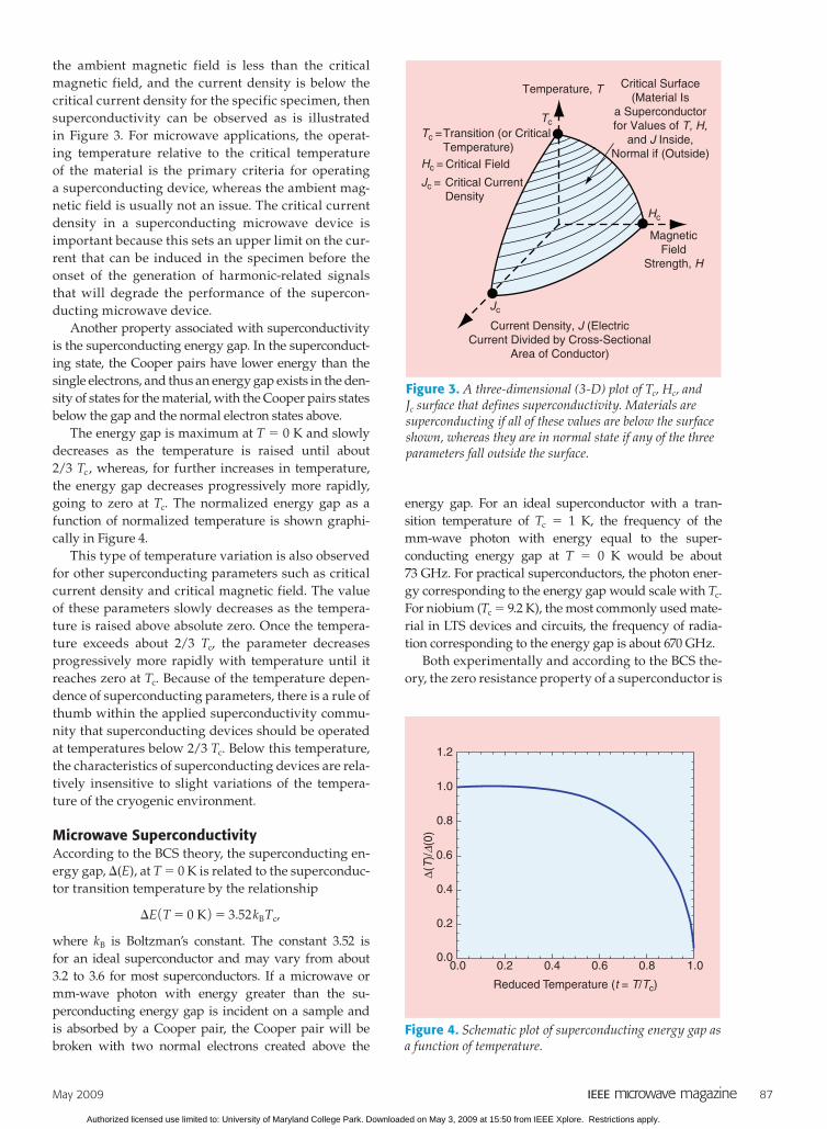
the ambient magnetic field is less than the critical magnetic field, and the current density is below the critical current density for the specific specimen, then superconductivity can be observed as is illustrated in Figure 3. For microwave applications, the operat-ing temperature relative to the critical temperature of the material is the primary criteria for operating a superconducting device, whereas the ambient mag-netic field is usually not an issue. The critical current density in a superconducting microwave device is important because this sets an upper limit on the cur-rent that can be induced in the specimen before the onset of the generation of harmonic-related signals that will degrade the performance of the supercon-ducting microwave device.
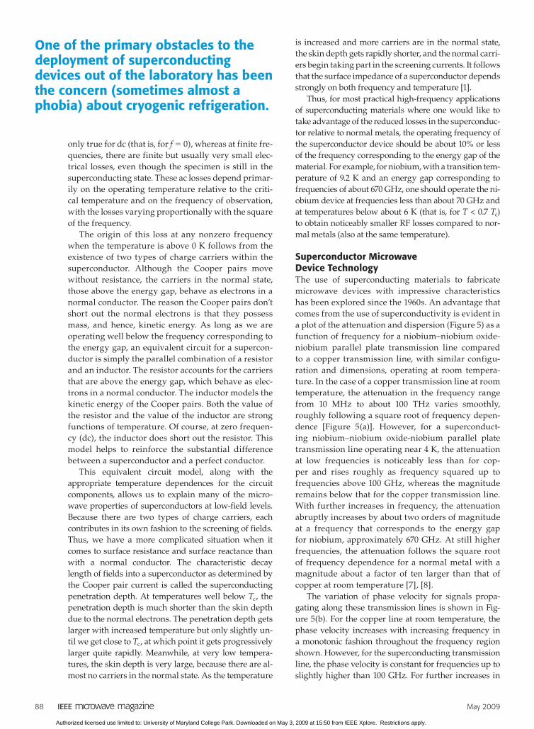
Another property associated with superconductivity is the superconducting energy gap. In the superconduct-ing state, the Cooper pairs have lower energy than the single electrons, and thus an energy gap exists in the den-sity of states for the material, with the Cooper pairs states below the gap and the normal electron states above.
The energy gap is maximum at T 5 0 K and slowly decreases as the temperature is raised until about 2/3 Tc , whereas, for further increases in temperature, the energy gap decreases progressively more rapidly, going to zero at Tc. The normalized energy gap as a function of normalized temperature is shown graphi-cally in Figure 4.
This type of temperature variation is also observed for other superconducting parameters such as critical current density and critical magnetic field. The value of these parameters slowly decreases as the tempera-ture is raised above absolute zero. Once the tempera-ture exceeds about 2/3 Tc, the parameter decreases progressively more rapidly with temperature until it reaches zero at Tc. Because of the temperature depen-dence of superconducting parameters, there is a rule of thumb within the applied superconductivity commu-nity that superconducting devices should be operated at temperatures below 2/3 Tc. Below this temperature, the characteristics of superconducting devices are rela-tively insensitive to slight variations of the tempera-ture of the cryogenic environment.
Microwave SuperconductivityAccording to the BCS theory, the superconducting en-ergy gap, D(E), at T 5 0 K is related to the superconduc-tor transition temperature by the relationship
DE 1T5 0 K 2 5 3.52 kB Tc,
where kB is Boltzman’s constant. The constant 3.52 is for an ideal superconductor and may vary from about 3.2 to 3.6 for most superconductors. If a microwave or mm-wave photon with energy greater than the su-perconducting energy gap is incident on a sample and is absorbed by a Cooper pair, the Cooper pair will be broken with two normal electrons created above the
energy gap. For an ideal superconductor with a tran-sition temperature of Tc 5 1 K, the frequency of the mm-wave photon with energy equal to the super-conducting energy gap at T 5 0 K would be about 73 GHz. For practical superconductors, the photon ener-gy corresponding to the energy gap would scale with Tc. For niobium (Tc 5 9.2 K), the most commonly used mate-rial in LTS devices and circuits, the frequency of radia-tion corresponding to the energy gap is about 670 GHz.
Both experimentally and according to the BCS the-ory, the zero resistance property of a superconductor is
Temperature, T
Current Density, J (ElectricCurrent Divided by Cross-Sectional
Area of Conductor)
MagneticField
Strength, H
TcTc =
Hc
Jc
Critical Surface(Material Is
a Superconductorfor Values of T, H,
and J Inside,Normal if (Outside)
Transition (or CriticalTemperature)
Hc = Critical Field
Jc = Critical CurrentDensity
Figure 3. A three-dimensional (3-D) plot of Tc, Hc, and Jc surface that defines superconductivity. Materials are superconducting if all of these values are below the surface shown, whereas they are in normal state if any of the three parameters fall outside the surface.
0.00.0 0.2 0.4
Reduced Temperature (t = T/Tc)
0.6 0.8 1.0
0.2
0.4
Δ(T
)/Δ(
0)
0.6
0.8
1.0
1.2
Figure 4. Schematic plot of superconducting energy gap as a function of temperature.
Authorized licensed use limited to: University of Maryland College Park. Downloaded on May 3, 2009 at 15:50 from IEEE Xplore. Restrictions apply.
88 May 2009
only true for dc (that is, for f 5 0), whereas at finite fre-quencies, there are finite but usually very small elec-trical losses, even though the specimen is still in the superconducting state. These ac losses depend primar-ily on the operating temperature relative to the criti-cal temperature and on the frequency of observation, with the losses varying proportionally with the square of the frequency.
The origin of this loss at any nonzero frequency when the temperature is above 0 K follows from the existence of two types of charge carriers within the superconductor. Although the Cooper pairs move without resistance, the carriers in the normal state, those above the energy gap, behave as electrons in a normal conductor. The reason the Cooper pairs don’t short out the normal electrons is that they possess mass, and hence, kinetic energy. As long as we are operating well below the frequency corresponding to the energy gap, an equivalent circuit for a supercon-ductor is simply the parallel combination of a resistor and an inductor. The resistor accounts for the carriers that are above the energy gap, which behave as elec-trons in a normal conductor. The inductor models the kinetic energy of the Cooper pairs. Both the value of the resistor and the value of the inductor are strong functions of temperature. Of course, at zero frequen-cy (dc), the inductor does short out the resistor. This model helps to reinforce the substantial difference between a superconductor and a perfect conductor.
This equivalent circuit model, along with the appropriate temperature dependences for the circuit components, allows us to explain many of the micro-wave properties of superconductors at low-field levels. Because there are two types of charge carriers, each contributes in its own fashion to the screening of fields. Thus, we have a more complicated situation when it comes to surface resistance and surface reactance than with a normal conductor. The characteristic decay length of fields into a superconductor as determined by the Cooper pair current is called the superconducting penetration depth. At temperatures well below Tc , the penetration depth is much shorter than the skin depth due to the normal electrons. The penetration depth gets larger with increased temperature but only slightly un-til we get close to Tc , at which point it gets progressively larger quite rapidly. Meanwhile, at very low tempera-tures, the skin depth is very large, because there are al-most no carriers in the normal state. As the temperature
is increased and more carriers are in the normal state, the skin depth gets rapidly shorter, and the normal carri-ers begin taking part in the screening currents. It follows that the surface impedance of a superconductor depends strongly on both frequency and temperature [1].
Thus, for most practical high-frequency applications of superconducting materials where one would like to take advantage of the reduced losses in the superconduc-tor relative to normal metals, the operating frequency of the superconductor device should be about 10% or less of the frequency corresponding to the energy gap of the material. For example, for niobium, with a transition tem-perature of 9.2 K and an energy gap corresponding to frequencies of about 670 GHz, one should operate the ni-obium device at frequencies less than about 70 GHz and at temperatures below about 6 K (that is, for T < 0.7 Tc) to obtain noticeably smaller RF losses compared to nor-mal metals (also at the same temperature).
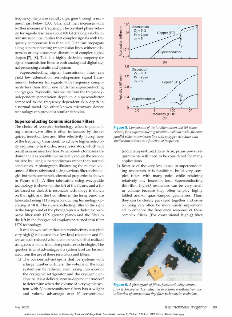
Superconductor Microwave Device TechnologyThe use of superconducting materials to fabricate microwave devices with impressive characteristics has been explored since the 1960s. An advantage that comes from the use of superconductivity is evident in a plot of the attenuation and dispersion (Figure 5) as a function of frequency for a niobium– niobium oxide-niobium parallel plate transmission line compared to a copper transmission line, with similar configu-ration and dimensions, operating at room tempera-ture. In the case of a copper transmission line at room temperature, the attenuation in the frequency range from 10 MHz to about 100 THz varies smoothly, roughly following a square root of frequency depen-dence [Figure 5(a)]. However, for a superconduct-ing niobium–niobium oxide-niobium parallel plate transmission line operating near 4 K, the attenuation at low frequencies is noticeably less than for cop-per and rises roughly as frequency squared up to frequencies above 100 GHz, whereas the magnitude remains below that for the copper transmission line. With further increases in frequency, the attenuation abruptly increases by about two orders of magnitude at a frequency that corresponds to the energy gap for niobium, approximately 670 GHz. At still higher frequencies, the attenuation follows the square root of frequency dependence for a normal metal with a magnitude about a factor of ten larger than that of copper at room temperature [7], [8].
The variation of phase velocity for signals propa-gating along these transmission lines is shown in Fig-ure 5(b). For the copper line at room temperature, the phase velocity increases with increasing frequency in a monotonic fashion throughout the frequency region shown. However, for the superconducting transmission line, the phase velocity is constant for frequencies up to slightly higher than 100 GHz. For further increases in
One of the primary obstacles to the deployment of superconducting devices out of the laboratory has been the concern (sometimes almost a phobia) about cryogenic refrigeration.
Authorized licensed use limited to: University of Maryland College Park. Downloaded on May 3, 2009 at 15:50 from IEEE Xplore. Restrictions apply.
May 2009 89
frequency, the phase velocity dips, goes through a min-imum just below 1,000 GHz, and then increases with further increase in frequency. The constant phase veloc-ity for signals less than about 100 GHz along a niobium transmission line implies that complex signals with fre-quency components less than 100 GHz can propagate along superconducting transmission lines without dis-persion or any associated distortion of complex signal shapes [7], [8]. This is a highly desirable property for signal transmission lines in both analog and digital sig-nal processing circuits and systems.
Superconducting signal transmission lines can yield low attenuation, zero-dispersion signal trans-mission behavior for signals with frequency compo-nents less than about one tenth the superconducting energy gap. Physically, this results from the frequency- independent penetration depth in a superconductor compared to the frequency-dependent skin depth in a normal metal. No other known microwave device technology can provide a similar behavior.
Superconducting Communications FiltersThe choice of resonator technology when implement-ing a microwave filter is often influenced by the re-quired insertion loss and filter selectivity (abruptness of the frequency transition). To achieve higher selectiv-ity requires, to first order, more resonators, which will result in more insertion loss. When conductor losses are dominant, it is possible to drastically reduce the resona-tor size by using superconductors rather than normal conductors. A photograph illustrating the relative vol-umes of filters fabricated using various filter technolo-gies but with comparable electrical properties is shown in Figure 6 [9]. A filter fabricating using waveguide technology is shown on the left of the figure, and a fil-ter based on dielectric resonator technology is shown on the right, and the two filters in the foreground are fabricated using HTS superconducting technology op-erating at 70 K. The superconducting filter to the right in the foreground of the photograph is a dielectric reso-nator filter with HTS ground planes and the filter to the left in the foreground employs patterned thin filter HTS technology.
It was shown earlier that superconductivity can yield very high Q-value (and thus low loss) resonators and fil-ters at much reduced volume compared with that realized using conventional (room temperature) technologies. The question is what advantages at a system level can be real-ized from the use of these resonators and filters.
The obvious advantage is that for systems with 1) a large number of filters, the volume of the total system can be reduced, even taking into account the cryogenic refrigerator and the cryogenic en-closure. It is a delicate system-dependent tradeoff to determine when the volume of a cryogenic sys-tem with N superconductor filters has a weight and volume advantage over N conventional
(room temperature) filters. Also, prime power re-quirements will need to be considered for many applications.
Because of the very low losses in superconduct-2) ing resonators, it is feasible to build very com-plex filters with many poles while retaining relatively low insertion loss. Superconducting thin-film, high-Q resonators can be very small in volume because they often employ highly folded and/or quasi-lumped geometries. Thus, they can be closely packaged together and cross coupling can often be more easily implement-ed to enhance the frequency response of these complex filters. (For conventional high-Q filter
Figure 6. A photograph of filters fabricated using various filter technologies. The reduction in volume resulting from the utilization of superconducting filter technologies is obvious.
Attenuation
Dispersion
Copper (RT)
104
102
1
Atte
nuat
ion
(dB
/mm
)V
eloc
ity (
108
m/s
)
10–2
1.6
1.2
0.8
0.4
00.01 1 100
Frequency (GHz)104
10–4
Copper (RT)
Superconductor
(a)
(b)
SuperconductorEg
Eg
Z0 = 6 ΩW = 2 μmε0 = 5
Z0 = 6 ΩW = 2 μmε0 = 5
Figure 5. Comparison of the (a) attenuation and (b) phase velocity for a superconducting niobium–niobium oxide–niobium parallel plate transmission line with a copper structure with similar dimensions, as a function of frequency.
Authorized licensed use limited to: University of Maryland College Park. Downloaded on May 3, 2009 at 15:50 from IEEE Xplore. Restrictions apply.

90 May 2009
technologies, the dimensions of the resonator are relatively large (~l/2) and thus achiev-ing cross coupling for a high complexity filter can be more difficult.) For conventional technologies, a 10–12- resonator filter is about the limit of complexity that can be practically
realized. With thin film superconducting filter technology, bandpass filters with as many as 22 poles have been fabricated and evaluated in the laboratory, as shown in Figure 7 [10]. Filters with this level of complexity are not practical with room-temperature filter technologies. The cryogenic environment required for the HTS 3) filter can also be employed to improve the perfor-mance of other components of the system, such as a low-noise amplifier (LNA) or passive mi-crowave device. The noise temperature of many semiconductor LNAs is known to decrease as the operating temperature is lowered; in cooling from room temperature to near 77 K, the noise temperature of the LNA will be reduced, typical-ly by a factor of 2 to 3. In addition, the contribu-tion to the total noise figure of the system from a passive component, such as a filter or transmis-sion line, depends on the insertion loss and on the ratio of the operating temperature compared to room temperature. Thus, the noise contribu-tion to system performance from a passive com-ponent operating at 77 K can be about one fourth the contribution to the noise temperature of the system when operated at room temperature.
In a communications application, for example, a cryogenic front-end system consisting of supercon-ducting filters, cryogenically cooled LNAs, and other passive components will have the following advantag-es compared to a room temperature version:
decreased noise figure for the system within the 1) bandpass of the filter and much steeper frequency roll-off on the edges of 2) the bandpass of the HTS filter due to the higher order filter that can be used and the higher Q values of the HTS resonators.
These characteristics have made HTS technology attractive to the wireless communications vendors who frequently have strong interference problems, which can be minimized by the use of an HTS filter and the lower noise figure of the cryogenic system. Shortly after the discovery of HTS materials, these features motivated more than a dozen companies worldwide to attempt to build, using either thalli-um-based or yttrium-based copper-oxide HTS, com-mercial systems that would satisfy the needs of the wireless communications vendors. Most of these companies have gone out of business, and only STI, Santa Barbara, California, is still aggressively pursu-ing deployment of HTS filter systems in the wireless communications community (see Table 1). To date, they have installed more than 6,000 HTS base station filter systems, mostly within the United States, where-as the number of systems deployed by their now de-funct competitors probably totaled less than several hundred. A recent photograph of a system built by STI is shown in Figure 8 [11].
Figure 8. Photograph of superconducting filter system for wireless telecommunication base station consisting of six HTS filters (each integrated with a cryogenically cooled LNA), a cryogenic refrigerator, and associated control electronics. The unit is 8 in high by 19 in deep by 11 in wide and weighs 34 lb. (Courtesy of Superconductor Technologies, Inc., Santa Barbara, California.)
00
–20
–40
–60
–80
–100
–1201935 1940 1945 1950 1955 1960 1965
Frequency [MHz]
⏐S21
⏐ [d
B]
⏐S11
⏐ [d
B]
–10
–20
–30
–40
–50
–60
Figure 7. Response of a 22-pole, ten-transmission-zero superconducting filter with performance exceeding a 50-pole Chebyhshev response.
Josephson digital circuits, fabricated using 1-mm design rules, can switch at rates corresponding to at least 770 GHz.
Authorized licensed use limited to: University of Maryland College Park. Downloaded on May 3, 2009 at 15:50 from IEEE Xplore. Restrictions apply.
May 2009 91
Microwave Superconductivity for High-Energy Physics ApplicationsMicrowave superconductivity has a long history in the high-energy physics (HEP) community for use in high-energy particle accelerators. In the early days of HEP accelerators, starting in the 1930s, particle accelera-tion was done in cyclotrons, which usually consisted of two large iron pole pieces of an electromagnet located on either side of a vacuum chamber in which the ion-ized particles were introduced. However, the maximum energy for ionized particles that could be realized from these machines was limited by the maximum field that could be obtained from air-core iron magnet systems.
In the 1960s and 1970s, the HEP community be-gan to consider the use of superconducting magnets. These magnets could provide a much higher mag-netic field than could be achieved from air-core iron magnets. The superconducting magnets that were used were long solenoidal dipole magnets that were located in a circular path, along which the particles were confined to travel.
To increase the energy of the ionized particles as they traveled around the circular path along the axes of the superconducting solenoidal magnets, high-Q value RF cavities, which possess a high electric field gradient, are located along the circular path. The larger the magnitude of the field gradient that the particle ex-periences, the greater the energy boost per transit. In order to realize the maximum energy boost per tran-sit, the accelerator engineers were forced to consider superconducting cavities. The Q-value of a resonator is given by
Q5Energy stored in the volume of the cavity
Energy absorbed in the surface of the cavity .
If one minimizes the losses in the walls of the cavity by using superconducting surfaces, whose losses are significantly smaller than for normal metals, the Q value will be increased. Furthermore, by optimizing the design of the cavity and by minimizing electric-field breakdown from imperfections in the surface of the cavity, the energy stored within the cavity could be increased, and along some path through the vol-ume of the cavity, a very high value of electric field gradient will be realized.
Typically, these 3-D RF cavities for HEP accelera-tors were fabricated using either bulk niobium foil formed into the desired shape of one half of the cavity structure or by niobium-plated copper stock that has been machined into the desired shapes. Once these hemispherical structures have been suitably coated or machined, they are welded together to form the reso-nators. One of the crucial obstacles to the use of these cavities is the need to chemically process and polish the internal surfaces of the cavities to minimize im-purities and to remove all physical imperfections that
might support premature electric field breakdowns, limiting the maximum field gradient that these cavi-ties could support. Physicists and engineers working in various national HEP laboratories around the world largely did the design and manufacturing of these superconducting RF cavities.
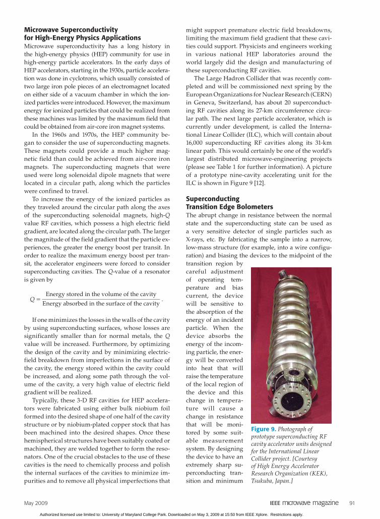
The Large Hadron Collider that was recently com-pleted and will be commissioned next spring by the European Organizations for Nuclear Research (CERN) in Geneva, Switzerland, has about 20 superconduct-ing RF cavities along its 27-km circumference circu-lar path. The next large particle accelerator, which is currently under development, is called the Interna-tional Linear Collider (ILC), which will contain about 16,000 superconducting RF cavities along its 31-km linear path. This would certainly be one of the world’s largest distributed microwave-engineering projects (please see Table 1 for further information). A picture of a prototype nine-cavity accelerating unit for the ILC is shown in Figure 9 [12].
Superconducting Transition Edge BolometersThe abrupt change in resistance between the normal state and the superconducting state can be used as a very sensitive detector of single particles such as X-rays, etc. By fabricating the sample into a narrow, low-mass structure (for example, into a wire configu-ration) and biasing the devices to the midpoint of the transition region by careful adjustment of operating tem-perature and bias current, the device will be sensitive to the absorption of the energy of an incident particle. When the device absorbs the energy of the incom-ing particle, the ener-gy will be converted into heat that will raise the temperature of the local region of the device and this change in tempera-ture will cause a change in resistance that will be moni-tored by some suit-able measurement system. By designing the device to have an extremely sharp su-perconducting tran-sition and minimum
Figure 9. Photograph of prototype superconducting RF cavity accelerator units designed for the International Linear Collider project. [Courtesy of High Energy Accelerator Research Organization (KEK), Tsukuba, Japan.]
Authorized licensed use limited to: University of Maryland College Park. Downloaded on May 3, 2009 at 15:50 from IEEE Xplore. Restrictions apply.
92 May 2009
mass, very sensitive transition edge bolometers have been built and used for a variety of applications, both scientific as well as a civilian.
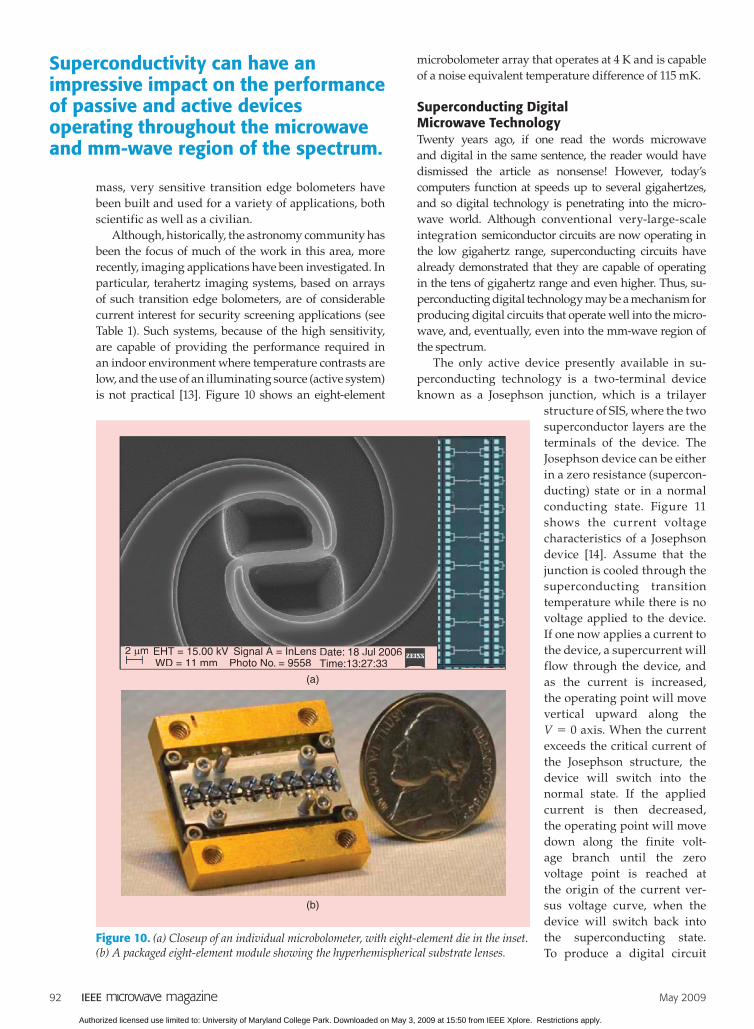
Although, historically, the astronomy community has been the focus of much of the work in this area, more recently, imaging applications have been investigated. In particular, terahertz imaging systems, based on arrays of such transition edge bolometers, are of considerable current interest for security screening applications (see Table 1). Such systems, because of the high sensitivity, are capable of providing the performance required in an indoor environment where temperature contrasts are low, and the use of an illuminating source (active system) is not practical [13]. Figure 10 shows an eight-element
microbolometer array that operates at 4 K and is capable of a noise equivalent temperature difference of 115 mK.
Superconducting Digital Microwave TechnologyTwenty years ago, if one read the words microwave and digital in the same sentence, the reader would have dismissed the article as nonsense! However, today’s computers function at speeds up to several gigahertzes, and so digital technology is penetrating into the micro-wave world. Although conventional very-large-scale integration semiconductor circuits are now operating in the low gigahertz range, superconducting circuits have already demonstrated that they are capable of operating in the tens of gigahertz range and even higher. Thus, su-perconducting digital technology may be a mechanism for producing digital circuits that operate well into the micro-wave, and, eventually, even into the mm-wave region of the spectrum.
The only active device presently available in su-perconducting technology is a two-terminal device known as a Josephson junction, which is a trilayer
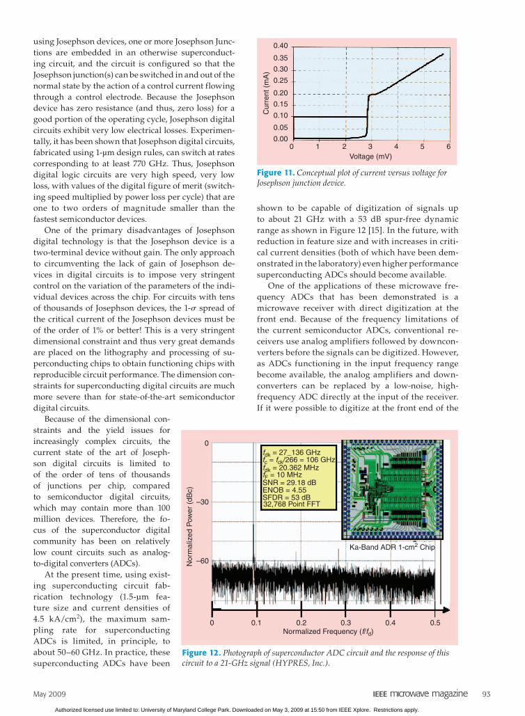
structure of SIS, where the two superconductor layers are the terminals of the device. The Josephson device can be either in a zero resistance (supercon-ducting) state or in a normal conducting state. Figure 11 shows the current voltage characteristics of a Josephson device [14]. Assume that the junction is cooled through the superconducting transition temperature while there is no voltage applied to the device. If one now applies a current to the device, a supercurrent will flow through the device, and as the current is increased, the operating point will move vertical upward along the V 5 0 axis. When the current exceeds the critical current of the Josephson structure, the device will switch into the normal state. If the applied current is then decreased, the operating point will move down along the finite volt-age branch until the zero voltage point is reached at the origin of the current ver-sus voltage curve, when the device will switch back into the superconducting state. To produce a digital circuit
2 µm EHT = 15.00 kVWD = 11 mm
Signal A = InLensPhoto No. = 9558
Date: 18 Jul 2006Time:13:27:33
(a)
(b)
222 µm EHT = 15.00 kVWD = 11 mm
Signal A = InLensPhoto No. = 9558
Date: 18 Jul 2006Time:13:27:33
Figure 10. (a) Closeup of an individual microbolometer, with eight-element die in the inset. (b) A packaged eight-element module showing the hyperhemispherical substrate lenses.
Superconductivity can have an impressive impact on the performance of passive and active devices operating throughout the microwave and mm-wave region of the spectrum.
Authorized licensed use limited to: University of Maryland College Park. Downloaded on May 3, 2009 at 15:50 from IEEE Xplore. Restrictions apply.
May 2009 93
using Josephson devices, one or more Josephson Junc-tions are embedded in an otherwise superconduct-ing circuit, and the circuit is configured so that the Josephson junction(s) can be switched in and out of the normal state by the action of a control current flowing through a control electrode. Because the Josephson device has zero resistance (and thus, zero loss) for a good portion of the operating cycle, Josephson digital circuits exhibit very low electrical losses. Experimen-tally, it has been shown that Josephson digital circuits, fabricated using 1-µm design rules, can switch at rates corresponding to at least 770 GHz. Thus, Josephson digital logic circuits are very high speed, very low loss, with values of the digital figure of merit (switch-ing speed multiplied by power loss per cycle) that are one to two orders of magnitude smaller than the fastest semicon ductor devices.
One of the primary disadvantages of Josephson digital technology is that the Josephson device is a two-terminal device without gain. The only approach to circumventing the lack of gain of Josephson de-vices in digital circuits is to impose very stringent control on the variation of the parameters of the indi-vidual devices across the chip. For circuits with tens of thousands of Josephson devices, the 1-s spread of the critical current of the Josephson devices must be of the order of 1% or better! This is a very stringent dimensional constraint and thus very great demands are placed on the lithography and processing of su-perconducting chips to obtain functioning chips with reproducible circuit performance. The dimension con-straints for superconducting digital circuits are much more severe than for state-of-the-art semiconductor digital circuits.
Because of the dimensional con-straints and the yield issues for increasingly complex circuits, the current state of the art of Joseph-son digital circuits is limited to of the order of tens of thousands of junctions per chip, compared to semiconductor digital circuits, which may contain more than 100 million devices. Therefore, the fo-cus of the superconductor digital community has been on relatively low count circuits such as analog-to-digital converters (ADCs).
At the present time, using exist-ing superconducting circuit fab-rication technology (1.5-µm fea-ture size and current densities of 4.5 kA/cm2), the maximum sam-pling rate for superconducting ADCs is limited, in principle, to about 50–60 GHz. In practice, these superconducting ADCs have been
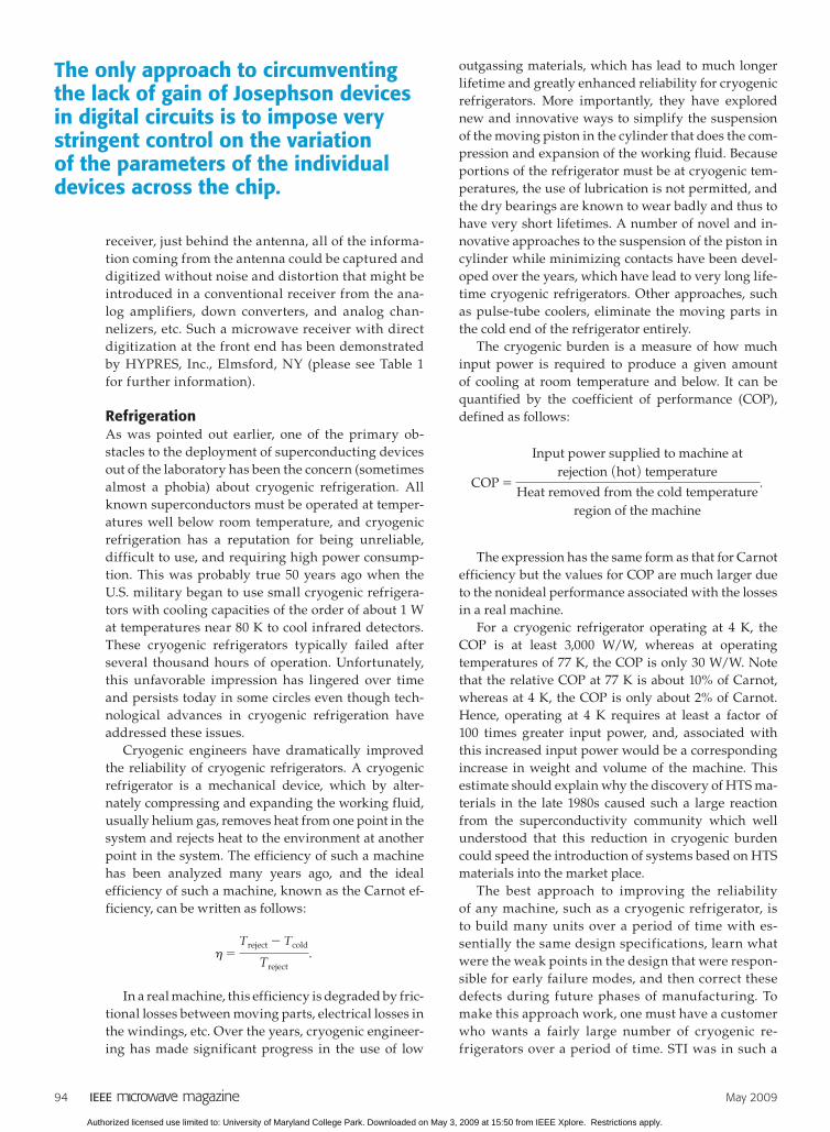
shown to be capable of digitization of signals up to about 21 GHz with a 53 dB spur-free dynamic range as shown in Figure 12 [15]. In the future, with reduction in feature size and with increases in criti-cal current densities (both of which have been dem-onstrated in the laboratory) even higher performance superconducting ADCs should become available.
One of the applications of these microwave fre-quency ADCs that has been demonstrated is a microwave receiver with direct digitization at the front end. Because of the frequency limitations of the current semiconductor ADCs, conventional re-ceivers use analog amplifiers followed by downcon-verters before the signals can be digitized. However, as ADCs functioning in the input frequency range become available, the analog amplifiers and down-converters can be replaced by a low-noise, high-frequency ADC directly at the input of the receiver. If it were possible to digitize at the front end of the
0fdk = 27_136 GHz
fdk = 20.362 MHzfF = 10 MHzSNR = 29.18 dBENOB = 4.55SFDR = 53 dB32,768 Point FFT
fc = fck/266 = 106 GHz
Nor
mal
ized
Pow
er (
dBc)
–30
–60
0 0.1 0.2 0.3 0.4 0.5Normalized Frequency (f/fd)
Ka-Band ADR 1-cm2 Chip
Figure 12. Photograph of superconductor ADC circuit and the response of this circuit to a 21-GHz signal (HYPRES, Inc.).
0.40
0.35
0.30
0.25
0.20
0.15
0.10
0.05
Cur
rent
(m
A)
0.000 1 2 3 4
Voltage (mV)5 60 1 2 3 4 5 6
Figure 11. Conceptual plot of current versus voltage for Josephson junction device.
Authorized licensed use limited to: University of Maryland College Park. Downloaded on May 3, 2009 at 15:50 from IEEE Xplore. Restrictions apply.
94 May 2009
receiver, just behind the antenna, all of the informa-tion coming from the antenna could be captured and digitized without noise and distortion that might be introduced in a conventional receiver from the ana-log amplifiers, down converters, and analog chan-nelizers, etc. Such a microwave receiver with direct digitization at the front end has been demonstrated by HYPRES, Inc., Elmsford, NY (please see Table 1 for further information).
RefrigerationAs was pointed out earlier, one of the primary ob-stacles to the deployment of superconducting devices out of the laboratory has been the concern (sometimes almost a phobia) about cryogenic refrigeration. All known superconductors must be operated at temper-atures well below room temperature, and cryogenic refrigeration has a reputation for being unreliable, difficult to use, and requiring high power consump-tion. This was probably true 50 years ago when the U.S. military began to use small cryogenic refrigera-tors with cooling capacities of the order of about 1 W at temperatures near 80 K to cool infrared detectors. These cryogenic refrigerators typically failed after several thousand hours of operation. Unfortunately, this unfavorable impression has lingered over time and persists today in some circles even though tech-nological advances in cryogenic refrigeration have addressed these issues.
Cryogenic engineers have dramatically improved the reliability of cryogenic refrigerators. A cryogenic refrigerator is a mechanical device, which by alter-nately compressing and expanding the working fluid, usually helium gas, removes heat from one point in the system and rejects heat to the environment at another point in the system. The efficiency of such a machine has been analyzed many years ago, and the ideal efficiency of such a machine, known as the Carnot ef-ficiency, can be written as follows:
h5Treject2 Tcold
Treject.
In a real machine, this efficiency is degraded by fric-tional losses between moving parts, electrical losses in the windings, etc. Over the years, cryogenic engineer-ing has made significant progress in the use of low
outgassing materials, which has lead to much longer lifetime and greatly enhanced reliability for cryogenic refrigerators. More importantly, they have explored new and innovative ways to simplify the suspension of the moving piston in the cylinder that does the com-pression and expansion of the working fluid. Because portions of the refrigerator must be at cryogenic tem-peratures, the use of lubrication is not permitted, and the dry bearings are known to wear badly and thus to have very short lifetimes. A number of novel and in-novative approaches to the suspension of the piston in cylinder while minimizing contacts have been devel-oped over the years, which have lead to very long life-time cryogenic refrigerators. Other approaches, such as pulse-tube coolers, eliminate the moving parts in the cold end of the refrigerator entirely.
The cryogenic burden is a measure of how much input power is required to produce a given amount of cooling at room temperature and below. It can be quantified by the coefficient of performance (COP), defined as follows:
COP5
Input power supplied to machine atrejection 1hot 2 temperature
Heat removed from the cold temperatureregion of the machine
.
The expression has the same form as that for Carnot efficiency but the values for COP are much larger due to the nonideal performance associated with the losses in a real machine.
For a cryogenic refrigerator operating at 4 K, the COP is at least 3,000 W/W, whereas at operating temperatures of 77 K, the COP is only 30 W/W. Note that the relative COP at 77 K is about 10% of Carnot, whereas at 4 K, the COP is only about 2% of Carnot. Hence, operating at 4 K requires at least a factor of 100 times greater input power, and, associated with this increased input power would be a corresponding increase in weight and volume of the machine. This estimate should explain why the discovery of HTS ma-terials in the late 1980s caused such a large reaction from the superconductivity community which well understood that this reduction in cryogenic burden could speed the introduction of systems based on HTS materials into the market place.
The best approach to improving the reliability of any machine, such as a cryogenic refrigerator, is to build many units over a period of time with es-sentially the same design specifications, learn what were the weak points in the design that were respon-sible for early failure modes, and then correct these defects during future phases of manufacturing. To make this approach work, one must have a customer who wants a fairly large number of cryogenic re-frigerators over a period of time. STI was in such a
The only approach to circumventing the lack of gain of Josephson devices in digital circuits is to impose very stringent control on the variation of the parameters of the individual devices across the chip.
Authorized licensed use limited to: University of Maryland College Park. Downloaded on May 3, 2009 at 15:50 from IEEE Xplore. Restrictions apply.
May 2009 95
position when they required higher cooling powers than were typically required for cryocooled IR ap-plications to cool HTS filter systems for the wire-less telecommunications networks. STI licensed a cryogenic refrigerator design concept from SunPow-er, Inc. (Athens, Ohio) and began to build them in quantity. Initially, the cryogenic refrigerators built by STI typically failed after several thousands of hours of operation. But with careful and diligent re-design, they have developed a cryogenic refrigerator suitable for a HTS wireless base station filter system applications that has very impressive reliability sta-tistics. As of late 2007, STI has deployed more than 6,000 systems that have accumulated more than 200,000,000 h of operation. Each cryogenic refrigera-tor, on the average, has operated for about four years. The number of failure of the total system was such that the mean time before failure (MTBF) can be de-duced to be greater than 500,000 h for the system. This MTBF corresponds to a failure rate of one per year for every 100 operating refrigerators. Note that this is the failure rate for the entire system, includ-ing the cryogenic refrigerator, cryogenic enclosure, HTS filters, and conventional electronics control-ling the operation of the wireless system. Accord-ing to STI, many of the failures reported were due to failures of conventional electrical components such as circuit boards and fans. This is an excellent demonstration that, with a large enough demand and careful design and manufacturing techniques, highly reliable cryogenic refrigerators can be made available on the commercial market place, and thus cryophobia should become a thing of the past in the minds of potential users of superconductivity.
ConclusionsSuperconductivity can have an impressive impact on the performance of passive and active devices operating throughout the microwave and mm-wave region of the spectrum. In these frequency ranges,
the electrical losses of superconductors are signifi-1) cantly less than the losses for normal conducting metallization in device and component applicationsactive superconducting Josephson device technol-2) ogy is inherently low loss and has demonstrated operation in excess of 700 GHz.
There has been much progress in the recent years to exploit superconductivity in selected microwave and mm-wave system. During a focus session (see Table 1) at IMS 2009 to be held in Boston in June 2009, there will be presentations dealing with the fol-lowing achievements:
the use of HTSs for very-low-loss, very sharp fre-1) quency roll-off filters in the wireless telecommu-nication front-end filter systems to reject out-of-band interference and reduce noise within band
the use of 3-D, high-2) Q niobium cavities at an op-erating temperature of 1.8 K for the accelerating elements in all of the current and future genera-tion of HEP particle accelerators the use of the very sharp superconductor-to-nor-3) mal transition as a sensitive bolometer detector in mm-wave imaging system for homeland secu-rity detection of objects hidden under clothingthe use of superconducting ADCs at the front end 4) of microwave receivers (just behind the antenna) to digitize the incoming signal to provide en-hanced signal extraction capabilities.
In addition to the advances in superconductor elec-tronic technology, here have been gains in the cryo-genic refrigeration community that can now provide energy-efficient, reliable cryogenic refrigeration systems, which should mitigate concerns associated with the use of cryogenic systems by the electronic engineering communities.
References[1] T. Van Duzer and C. W. Turner, Principles of Superconductive Devices
and Circuits. New York, NY: Elsevier North Holland, 1981.[2] M. Tinkham, Superconductivity. New York, NY: Gordon & Breach,
1965.[3] I. G. Bednorz and K. A. Müller, “Possible high-Tc superconduc-
tivity in Be-La-Cu-O system,” Zeit. für Phys., vol. B64, no. 2, pp. 189–191, 1986.
[4] H. K. Onnes, “Further experiments with liquid helium. C. On the change of electric resistance of pure metals at very low tem-peratures, etc. IV. The resistance of pure mercury at helium temperatures,” Commun. Phys. Lab. Univ. Leiden, vol. 11, no. 1206, pp. 17–19, 1911.
[5] J. Bardeen, L. N. Cooper, and J. R. Schreiffer, “Theory of supercon-ductivity,” Phys. Rev., vol. 108, no. 5, pp. 1175–1204, 1957.
[6] M. A. Biondi and M. P. Garfunkel, “Millimeter wave absorption in superconducting aluminum. I. Temperature dependence of the energy gap,” Phys. Rev., vol. 116, no. 4, pp. 853–861, Nov. 1959.
[7] R. L. Kautz, “Picosecond pulse propagation on superconducting striplines,” J. Appl. Phys., vol. 49, no. 1, pp. 308–314, Jan. 1978.
[8] E. B. Ekholm and S. W. McKnight, “Attenuation and dispersion for high-Tc superconducting microstrip lines,” IEEE Trans. Microwave Theory Tech., vol. 38, no. 4, pp. 387–395, Apr. 1990.
[9] R. R. Mansour, S. Yu, V. Dokas, B. Jolley, G. Thomson, W.-C. Tang, and C. M Kudsia, “Design considerations of superconductive in-put multiplexers for satellite applications,” IEEE Trans. Microwave Theory Tech., vol. 44, no. 7, pp. 1213–1228, July 1996.
[10] G. Tsuzuki, S. Ye, and S. Berkowitz, “Ultra-sensitive 22-pole, 10 transmission zero superconducting bandpass filter surpasses 50-pole Chebyhshev filter,” IEEE Trans. Microwave Theory Tech., vol. 50, no. 12, pp. 2924–2928, Dec. 2002.
[11] Superconductor Technologies, Inc., Santa Barbara, CA. [Online]. Available: www.suptech.com
[12] International Linear Collider. [Online]. Available: www.interactions.org/imagebank/search_detail.php?image_no=KE0116
[13] E. N. Grossman, C. R. Dietlein, M. Leivo, A. Rautiainen, and A. Luukanen, “A passive, real-time, terahertz camera for security screening, using superconducting microbolometers,” presented at the IEEE MTT-S International Microwave Symposium 2009, Bos-ton, MA, June 2009.
[14] L. A. Abelson and G. L. Kerber, “Superconductor integrated circuit fabrication technology,” Proc. IEEE, vol. 92, no. 10, pp. 1517–1531, Oct. 2004.
[15] D. E. Kirchenko, T. V. Filippov, and D. Gutpa, “Microwave receiver with direct digitization,” presented at the IEEE MTT-S Internation-al Microwave Symposium 2009, Boston, MA, June 2009.
Authorized licensed use limited to: University of Maryland College Park. Downloaded on May 3, 2009 at 15:50 from IEEE Xplore. Restrictions apply.