master thesis : oufti-2's on-orbit, hot reprogramming of ... · university of li ege faculty...
TRANSCRIPT

http://lib.ulg.ac.be http://matheo.ulg.ac.be
Master thesis : OUFTI-2's on-orbit, hot reprogramming of on-board computer
(OBC): design, implementation and tests
Auteur : Guillaume, Thibaut
Promoteur(s) : Verly, Jacques
Faculté : Faculté des Sciences appliquées
Diplôme : Master en ingénieur civil en informatique, à finalité spécialisée en "computer systems and networks"
Année académique : 2016-2017
URI/URL : http://hdl.handle.net/2268.2/2631
Avertissement à l'attention des usagers :
Tous les documents placés en accès ouvert sur le site le site MatheO sont protégés par le droit d'auteur. Conformément
aux principes énoncés par la "Budapest Open Access Initiative"(BOAI, 2002), l'utilisateur du site peut lire, télécharger,
copier, transmettre, imprimer, chercher ou faire un lien vers le texte intégral de ces documents, les disséquer pour les
indexer, s'en servir de données pour un logiciel, ou s'en servir à toute autre fin légale (ou prévue par la réglementation
relative au droit d'auteur). Toute utilisation du document à des fins commerciales est strictement interdite.
Par ailleurs, l'utilisateur s'engage à respecter les droits moraux de l'auteur, principalement le droit à l'intégrité de l'oeuvre
et le droit de paternité et ce dans toute utilisation que l'utilisateur entreprend. Ainsi, à titre d'exemple, lorsqu'il reproduira
un document par extrait ou dans son intégralité, l'utilisateur citera de manière complète les sources telles que
mentionnées ci-dessus. Toute utilisation non explicitement autorisée ci-avant (telle que par exemple, la modification du
document ou son résumé) nécessite l'autorisation préalable et expresse des auteurs ou de leurs ayants droit.

University of LiegeFaculty of Applied Sciences
OUFTI-2’s on-orbit, hot reprogramming of
on-board computer (OBC): design,
implementation and tests
Graduation Studies conducted for obtaining the Master’s degree inin Computer Science and Engineering
by Thibaut Guillaume.
Promoter: Prof. Jacques Verly
Academic year 2016-2017

Abstract
OUFTI-2’s on-orbit, hot reprogramming ofon-board computer (OBC): design,
implementation and tests
by Thibaut Guillaume
Promoter: Prof. Jacques VerlyAcademic year 2016-2017
Today embedded systems are used in many domains and they can executecomplex software. Reprogramming the systems is a functionality that canreally be useful to correct issues that could remain in the software at the endof the developments.In this work, the different methods that can be used to remotely reprogramembedded systems at run-time are explored. A solution to reprogram theon-board computer of the nanosatellite OUFTI-2 was designed and devel-oped. This solution is based on the sending of an entire new software to thesatellite, and the use of this new software instead of the previous one.A particular attention is given to the reliability of the transmission of thenew software. Indeed, having a corrupted software executed on the on-boardcomputer could lead to the failure of the missions of the satellite.This work describes the architecture of the solution, and how it was imple-mented. It also explains the different tests performed to ensure that thereprogramming mechanism works properly.
i

Acknowledgement
Being part of OUFTI-2 team was very rewarding and I would like to expressmy gratitude to the people who helped me during the realization of this thesis.
I would like first to thank Sebastien De Dijcker and Xavier Werner fortheir availability and the time they dedicated to help me in the realizationof this thesis.
I would also thank Prof. Jacques Verly for all the advice he gave me,especially regarding the redaction of this document.
A great thank to my friend and student colleague, Adrien Rikir, who devel-oped the on-board computer software. We worked a lot together to integratemy solution in his work.
Finally, many thanks to my family and friends who supported me duringthe realization of this thesis.
ii

Contents
Introduction 1
1 OUFTI-2 System 21.1 Architecture . . . . . . . . . . . . . . . . . . . . . . . . . . . . 21.2 Ground segment . . . . . . . . . . . . . . . . . . . . . . . . . . 2
1.2.1 Control segment . . . . . . . . . . . . . . . . . . . . . . 31.2.2 D-STAR segment . . . . . . . . . . . . . . . . . . . . . 4
1.3 Space segment . . . . . . . . . . . . . . . . . . . . . . . . . . . 51.3.1 Subsystems . . . . . . . . . . . . . . . . . . . . . . . . 51.3.2 OBC subsystem . . . . . . . . . . . . . . . . . . . . . . 61.3.3 Payloads . . . . . . . . . . . . . . . . . . . . . . . . . . 7
2 Review of reprogramming techniques and selection of themost appropriate one 92.1 Requirements . . . . . . . . . . . . . . . . . . . . . . . . . . . 92.2 Addressing and linking . . . . . . . . . . . . . . . . . . . . . . 102.3 Binary replacement . . . . . . . . . . . . . . . . . . . . . . . . 12
2.3.1 Full Binary replacement . . . . . . . . . . . . . . . . . 122.3.2 Partial binary replacement . . . . . . . . . . . . . . . . 13
2.4 Loadable modules . . . . . . . . . . . . . . . . . . . . . . . . . 132.4.1 Pre-linked modules . . . . . . . . . . . . . . . . . . . . 142.4.2 Dynamically linked modules . . . . . . . . . . . . . . . 152.4.3 Position independent modules . . . . . . . . . . . . . . 15
2.5 Virtual machines . . . . . . . . . . . . . . . . . . . . . . . . . 152.6 Design choice for OUFTI-2 . . . . . . . . . . . . . . . . . . . . 16
3 Architecture of the solution 183.1 Protocol for sending a new firmware . . . . . . . . . . . . . . . 18
iii

3.2 Organization of OBC . . . . . . . . . . . . . . . . . . . . . . . 203.3 Update functions in firmware . . . . . . . . . . . . . . . . . . 21
3.3.1 Send firmware packets . . . . . . . . . . . . . . . . . . 213.3.2 Initialize update . . . . . . . . . . . . . . . . . . . . . . 223.3.3 Send CRC . . . . . . . . . . . . . . . . . . . . . . . . . 233.3.4 Switch firmware . . . . . . . . . . . . . . . . . . . . . . 243.3.5 Check code version . . . . . . . . . . . . . . . . . . . . 25
3.4 Bootstrap loader . . . . . . . . . . . . . . . . . . . . . . . . . 253.5 On-ground software . . . . . . . . . . . . . . . . . . . . . . . . 26
4 Implementation details 294.1 Flash memory . . . . . . . . . . . . . . . . . . . . . . . . . . . 29
4.1.1 Flash memory organization . . . . . . . . . . . . . . . 294.1.2 Operation applicable on flash memory . . . . . . . . . 31
4.2 FRAM Memory . . . . . . . . . . . . . . . . . . . . . . . . . . 324.2.1 FRAM memory organization . . . . . . . . . . . . . . . 324.2.2 SPI bus . . . . . . . . . . . . . . . . . . . . . . . . . . 33
4.3 Bootstrap loader . . . . . . . . . . . . . . . . . . . . . . . . . 364.4 Protocols used . . . . . . . . . . . . . . . . . . . . . . . . . . . 37
4.4.1 AX.25 protocol . . . . . . . . . . . . . . . . . . . . . . 384.4.2 PUS protocol . . . . . . . . . . . . . . . . . . . . . . . 38
4.5 Telecommands and telemetries . . . . . . . . . . . . . . . . . . 394.5.1 Initialize update . . . . . . . . . . . . . . . . . . . . . . 394.5.2 Firmware sending . . . . . . . . . . . . . . . . . . . . . 404.5.3 CRC sending . . . . . . . . . . . . . . . . . . . . . . . 414.5.4 Switch between the firmwares . . . . . . . . . . . . . . 424.5.5 Code version checking . . . . . . . . . . . . . . . . . . 42
4.6 Reliability, computation of CRC . . . . . . . . . . . . . . . . . 424.6.1 Theory about the CRC . . . . . . . . . . . . . . . . . . 434.6.2 Implementation of the CRC . . . . . . . . . . . . . . . 44
4.7 Ground station software modifications . . . . . . . . . . . . . 444.8 Linker command file . . . . . . . . . . . . . . . . . . . . . . . 454.9 Reprogramming procedure . . . . . . . . . . . . . . . . . . . . 474.10 Initialization procedure . . . . . . . . . . . . . . . . . . . . . . 48
5 Tests 505.1 Flash memory based . . . . . . . . . . . . . . . . . . . . . . . 50
5.1.1 Configuration . . . . . . . . . . . . . . . . . . . . . . . 50
iv

5.1.2 Objectives . . . . . . . . . . . . . . . . . . . . . . . . . 515.1.3 Procedures . . . . . . . . . . . . . . . . . . . . . . . . . 515.1.4 Results . . . . . . . . . . . . . . . . . . . . . . . . . . . 52
5.2 FRAM memory based . . . . . . . . . . . . . . . . . . . . . . 525.2.1 Configuration . . . . . . . . . . . . . . . . . . . . . . . 525.2.2 Objectives . . . . . . . . . . . . . . . . . . . . . . . . . 535.2.3 Procedures . . . . . . . . . . . . . . . . . . . . . . . . . 545.2.4 Results . . . . . . . . . . . . . . . . . . . . . . . . . . . 54
5.3 Integration in OBC firmware . . . . . . . . . . . . . . . . . . . 545.3.1 Configuration . . . . . . . . . . . . . . . . . . . . . . . 545.3.2 Objectives . . . . . . . . . . . . . . . . . . . . . . . . . 555.3.3 Procedures . . . . . . . . . . . . . . . . . . . . . . . . . 565.3.4 Results . . . . . . . . . . . . . . . . . . . . . . . . . . . 56
5.4 Sending by AX.25 . . . . . . . . . . . . . . . . . . . . . . . . . 565.4.1 Configuration . . . . . . . . . . . . . . . . . . . . . . . 565.4.2 Objectives . . . . . . . . . . . . . . . . . . . . . . . . . 575.4.3 Procedures . . . . . . . . . . . . . . . . . . . . . . . . . 575.4.4 Results . . . . . . . . . . . . . . . . . . . . . . . . . . . 57
Conclusion 58
A Intel Hex File 60
B Code Composer Studio - Enabling the Hex file generation 62
C Code Composer Studio - Configuration for initialization 64
D Linker command files modifications 66
E Activity 70
v

List of Figures
1.1 Architecture of OUFTI-2 systems [7]. . . . . . . . . . . . . . . 31.2 D-STAR direct communication mode [7]. . . . . . . . . . . . . 41.3 D-STAR indirect communication mode [7]. . . . . . . . . . . . 41.4 Internal architecture of OUFTI-2 CubeSat [7]. . . . . . . . . . 51.5 Hardware Architecture of the OBC [7]. . . . . . . . . . . . . . 8
2.1 Illustration of relocation principle. . . . . . . . . . . . . . . . . 112.2 Reprogramming with dynamically linked modules. . . . . . . . 14
3.1 Sequence diagram of Update protocol. . . . . . . . . . . . . . 193.2 Activity diagram of firmware packet receiving. . . . . . . . . . 223.3 Activity diagram of switching function. . . . . . . . . . . . . . 243.4 Activity diagram of the bootstrap loader. . . . . . . . . . . . . 263.5 activity diagram of ground segment packet sending . . . . . . 27
4.1 Memory organization of MSP430f1611. . . . . . . . . . . . . . 304.2 Organization of FRAM Memory. . . . . . . . . . . . . . . . . . 344.3 Read operation on FRAM [5]. . . . . . . . . . . . . . . . . . . 354.4 Write operation on FRAM [5]. . . . . . . . . . . . . . . . . . . 354.5 Bootstrap copy - Phase 1. . . . . . . . . . . . . . . . . . . . . 37
5.1 Prototype of the OBC [7]. . . . . . . . . . . . . . . . . . . . . 55
B.1 Overview of the panel for Intel Hex File configuration. . . . . 63
C.1 Erase option selection in Code Composer Studio . . . . . . . . 65
E.1 Photo taken at the end of the OUFTI-2 project presentationat ESTEC. . . . . . . . . . . . . . . . . . . . . . . . . . . . . . 71
vi

List of Tables
4.1 Register values of the flash memory controller. . . . . . . . . . 324.2 FRAM opcodes. . . . . . . . . . . . . . . . . . . . . . . . . . . 364.3 AX.25 frame structure for OUFTI-2. . . . . . . . . . . . . . . 384.4 Organization of PUS telecommand for the sending of the firmware. 404.5 Organization of PUS telemetry for the sending of the firmware. 41
vii

List of Acronyms
AX.25 Amateur X.25.
BCN Beacon.
CRC Cyclic Redundancy Check.
ESA European Space Agency.
FRAM Ferroelectric Random Access Memory.
IDE Integrated Development Environment.
IMU Inertial Measurement unit.
OBC On-board computer.
OS Operating System.
OUFTI Orbital Utility For Telecommunication Innovation.
PUS Packet Utilization Standard.
RAM Random Access Memory.
SPI Serial Peripheral Interface.
viii

Introduction
Nowadays, embedded systems devices are widely used in many different appli-cations. Software that manage the devices become more and more powerful,allowing those devices to perform various complex operations. However, thesoftware capability improvement sometimes increases their complexity. Thiscreates more difficulties to test and correct issues before the exploitation ofthose systems. Like for traditional software, some issues that were not de-tected during test phase could thus be encountered during the use of theembedded systems.Software update is a process that is really useful to correct the issues. Thesimplest way to perform this operation is to plug the programmer tool onthe embedded device and change the software. However, this technique can-not be applied to all embedded devices. In fact, some of these devices arehardly or even totally physically inaccessible during their exploitation. Sys-tems must thus be developed to permit the software update when the deviceis not accessible.This thesis proposes a method that can be used to reprogram the on-boardcomputer of the nanosatellite OUFTI-2 from the ground. Indeed, the on-board computer software is rather complex and some issues could remain init after the satellite launch in space. Obviously, as the satellite in orbit willnot be physically accessible, a remote update mechanism from the ground isproposed.Chapter 1 presents the OUFTI-2 project. It discusses the aims of the projectand the overall OUFTI-2 system organization. Chapter 2 explains the dif-ferent reprogramming methods that were found in the literature. It alsoexplains and justifies the chosen method for OUFTI-2. Chapter 3 focuses onthe architecture of the proposed solution. Chapter 4 presents the implemen-tation details. Finally, chapter 5 explains the tests that were performed toensure that the reprogramming method is functional.
1

Chapter 1
OUFTI-2 System
OUFTI-2 like his predecessor OUFTI-1, is a CubeSat. The satellite is es-sentially a cube with sides of about 10 centimeters long. In this chapter,an overview of the global project architecture is presented in section 1, theexplanation of the systems used to control and exploit the satellite from theearth is discussed in section 2, and finally a general overview of the satelliteis exposed in section 3.
1.1 Architecture
The project can be seen as a composition of two systems called segments.The first is the ground segment with infrastructures and software deployedon the ground in order to control and communicate with the satellite.The second one is the space segment, which consist of the satellite containingthe hardware and software used for the mission.This organization is displayed on Fig.1.1. The two segments will be describedin sections 1.2 and 1.3.
1.2 Ground segment
As it can be observed in Fig.1.1, the ground segment is divided into two parts.The first is the control segment and the second one the D-STAR segment.
2

Figure 1.1: Architecture of OUFTI-2 systems [7].
1.2.1 Control segment
The aim of the control segment is to send instructions to the satellite andget information back from it. Instructions that are sent from the ground tothe satellite are called telecommands. Information sent to the ground arecalled telemetries. The telecommands and telemetries use the Amateur X.25(AX.25) protocol. This data link layer protocol is used to transfer data overradio waves.In Fig. 1.1, the control segment is separated in two components. The missioncontrol center is a computer and is used to prepare the sending of AX.25frames and process to ones received from the satellite. The ground station isthe infrastructure used to send radio waves (ie. radio transmitters, antennas,amplifiers).In addition to the telecommands and telemetries channels, a Beacon (BCN)receiver channel is also used. Indeed, the satellite regularly sends Morse-codesignals to provide basic parameters such as temperatures, voltages, and otherkey parameters to the ground.More explanations about the telecommands, telemetries, and ground stationsoftware will be provided in chapters 3 and 4. Indeed, On-board computer(OBC) reprogramming will be performed thanks to the control segment usingtelecommands and monitored using telemetries.
3

Figure 1.2: D-STAR direct communication mode [7].
Figure 1.3: D-STAR indirect communication mode [7].
1.2.2 D-STAR segment
D-STAR is a digital protocol able to transmit voice and data simultaneously.The OUFTI-2 primary mission is to bring a D-STAR repeater in space sothat users can communicate through this repeater.The communication using OUFTI-2 can either be direct or indirect. Directcommunication means that the two end users directly transmit data andvoice through the space repeater. This situation is presented in Fig. 1.2.
Indirect communication is the mode in which data and voice are forwardedusing a terrestrial relay and/or internet before or after being forwarded byOUFTI-2. A schema of this general situation is presented in Fig. 1.3.
As shown on Fig.1.1, the D-STAR segment is divided in two distinct parts.
4

The first part is a traditional D-STAR repeater which allows communicationsvia radio or internet links. And the second one is the satellite extensionswhich is the part necessary to make the link between OUFTI-2 and the D-STAR terrestrial repeater. The D-STAR ground segment is used when thecommunication mode is indirect.
1.3 Space segment
This section briefly describes the subsystems that are embedded in the satel-lite. A particular attention is given to the OBC as the reprogramming tech-niques presented in the next chapters will be applied to it. A global view ofthe satellite is displayed on Fig.1.4.
Figure 1.4: Internal architecture of OUFTI-2 CubeSat [7].
1.3.1 Subsystems
The satellite is composed of different subsystems that are assembled together.Some of them can be identified on Fig.1.4. In this section, only the commu-nication (COM) subsystem is briefly presented as it is the only subsystem
5

which is directly involved in the update chain, in addition to the OBC. In-formation about the other subsystems can be found in [7].The COM is the subsystem responsible of receiving and sending radio sig-nals. Its role is to modulate a signal to send information and demodulateit to receive data. This system deals with D-STAR, AX.25, and BCN. Thereception of telecommands and the sending of telemetry are done via thissubsystem.However, the AX.25 frame decoding and encoding are not performed by thissubsystem, the OBC is responsible for doing this operation.
1.3.2 OBC subsystem
The OBC is the subsystem which is responsible of globally managing thesatellite. It is used to get and treat requests from the ground. It also sendsback telemetries to give information about the different parameters describ-ing the state of the satellite. The OBC can activate and stop the differentsubsystems and payloads.The hardware architecture of this system is now fixed. It is presented onFig. 1.5. It can be observed that two MSP430 micro-controllers are usedand are both connected to a watchdog. That is the OBC-Redundancy prin-ciple. There is only one micro-controller that is powered at a given time andit must regularly send a signal to the watchdog in order to inform that itis still running without any problem. If the watchdog does not receive anysignal during 5 seconds, it will consider that a problem has been encounteredand will start the other micro-controller. This redundancy increases the re-liability of the OBC, and thus, the reliability of the whole satellite.An external 2 Mbits Ferroelectric Random Access Memory (FRAM) is alsoconnected to both micro-controllers. It is used to keep the different mea-surements performed on the satellite subsystems. It is also used to keep thecurrent state of the satellite. So if the second micro-controller is powered onfor any reason, it knows in which operating mode the satellite is and it cancontinue to perform the appropriate operations. Finally, part of the FRAMis used to perform the update as explained later in this document.A real time operating system is used to perform the different tasks. This op-erating system is FreeRTOS. Details about the OUFTI-1 on-board softwarecan be found in [6], but this software has been updated to a newer versionfor OUFTI-2’s mission by my student colleague Adrien Rikir.
6

1.3.3 Payloads
The primary mission of OUFTI-2 is to provide D-STAR repeating capabilityin space.In addition, two other payloads were added to the satellite. The first one isthe RAD subsystem. Electronic circuits are highly exposed to ionizing radi-ations in space. The aim of this payload is to test different types of shieldingagainst the radiations.The second one is a subsystem developed by high-school students (Sint-Pieterscollege, Jette, Belgium) which will be used to determine the attitude1
of the satellite. It is called the Inertial Measurement unit (IMU) subsystem.
1The attitude of a satellite is its orientation in the space with respect to a fixed reference
7

Figure 1.5: Hardware Architecture of the OBC [7].
8

Chapter 2
Review of reprogrammingtechniques and selection of themost appropriate one
In the literature, different methods have already been proposed to reprogramembedded systems at runtime. The solutions presented in this chapter havenot been exclusively used on satellites but give an overview of the differenttechniques available and serve as a base to choose the design of the OUFTI-2 reprogramming method. The chapter is divided in six sections. Section1 discusses the requirements for OUFTI-2’s mission. Section 2 talks abouttwo particular concepts that are important for understanding reprogrammingmechanisms. Sections 3, 4 and 5 present three general types of methodsused for runtime reprogramming. Section 6 describes and justifies the designchoice for OUFTI-2’s mission.
2.1 Requirements
The main purpose of reprogramming techniques for OUFTI-2’s mission is tocorrect mistakes that could remain in the OBC software after all the testingperformed on the ground. Indeed, some unknown issues could remain in theOBC software at launching time, and should potentially be corrected duringthe flight to avoid major problems.The first objective is to have a safe method and be sure that a reprogrammingprocess will not lead to a communication and control loss with the satellite.
9

Obviously, this situation would be critical as no physical access is possibleto manually correct the introduced failure. Mechanisms checking the newreceived program and ensuring that the satellite will still be accessible evenin case of an unexpected problem that could occur during the reprogrammingprocedure must be used.The second objective is to disturb as little as possible the routine operations.Indeed, the satellite must respond to telecommands and send telemetries.The time during which the OBC performs operations without giving anystatus to the ground must be as short as possible.Finally, the third requirement is to have a solution that does not consumetoo much memory of the micro-controllers. Indeed, this resource is limited onthe micro-controllers used. There are 48KB of program memory available.Similarly, the amount of Random Access Memory (RAM) on the micro-controllers is limited to 10KB. As the actual OBC software uses about 8KBof RAM, care must be taken to avoid RAM memory overflow during theupdate procedure.
2.2 Addressing and linking
A program in a micro-controller is composed of code and data. These arestored in the memory and are referenced by their addresses. To execute aprogram, jumping between the different addresses is necessary.However, the addressing can be performed in two ways: either absolute orrelative.In the absolute addressing method, the code and data are accessed directlyby their actual addresses. The references to functions and variables in thebinary code are their physical address. A code compiled using this methodcannot be moved as is to another location. Indeed, changing the position ofthis code without changing the absolute references to variables and functionscontained in it will cause jumping to wrong addresses and give incorrect be-havior.Changing the position of this type of code requires to relocate it. The relo-cation is the process in which absolute references to functions and variablesin the code are adjusted in order to fit with their new positions.The relocation principle is illustrated on Fig. 2.1. (A) shows the initial mem-ory configuration in which all references are correct. (B) shows that code hasbeen moved and references to function A are invalidated. (C) shows that the
10

Figure 2.1: Illustration of relocation principle.
relocation mechanism has been applied and reference to function A is againcorrect.
In the relative access method the references to variables and functions aredetermined based on the value of the program counter 1 on which an offsetrelative to it is added. In opposite to the first method, the code compiledwith this method can be moved without any modification. Indeed, referencesto variables and functions in this type of code are not absolute addresses butoffsets which are independent of the real position.A program can also be statically or dynamically linked.A statically linked one is a program in which all references to variables andfunctions are resolved at compile-time.In contrast, a program is said to be dynamically linked if some of these ref-erences are unknown at the end of the compilation process. At runtime adetermination of the references is needed to execute the program correctly.A linking procedure is thus performed at run-time.It is worth mentioning that the concept of addressing and linking are inde-pendent. Indeed, a code compiled using an absolute addressing method canbe either statically or dynamically linked.The two concepts of addressing and linking are the basis for understandingmethods described in the following sections.
1The program counter is a processor register which holds at any time the address ofthe currently executed instruction.
11

2.3 Binary replacement
If a code is statically linked, at the end of the linking process, a binary rep-resentation of the code is obtained. This one can directly be executed by themicro-controller, but provided that this code is placed at the right positionin program memory if absolute addressing is used.One solution proposed to reprogram embedded systems at runtime is a bi-nary replacement of/in the firmware2.TOSBoot [10], which is a method developed to reprogram sensors networksand the reprogramming procedure applied to ESTCube-1 CubeSat [15] presenta full firmware binary replacement. In their document, M. Iwinski and al.[11] also discuss the full binary replacement but also address the possibilityof partial firmware replacement.
2.3.1 Full Binary replacement
The idea of full binary replacement is to compile and link a new/updatedcode that can be executed at the position of the previous one. Then, thisbinary code is sent to the target that must be updated, where it replaces theold one by the received one.The program receiving the new binary code representation is the one on themicro-controller. The updated code cannot be directly placed at its finaldestination as it would overwrite the old code that is still running. It wouldresult in an undetermined behavior. The new binary representation is storedsomewhere else, this until the whole new firmware is received.When the complete firmware has been received by the destination, the micro-controller is rebooted and executes a special piece of code which is called thebootstrap loader. This code is at a fixed position in the program memoryof the micro-controller, independent of firmwares and cannot be changed.Its function is to erase the old firmware and replace it by the new one justreceived.The major drawback of this technique is that all the firmware must be re-transmitted even if the goal is to perform a little modification in the runningfirmware. Depending on the size of the code, this technique can consumetime and resources.However the solution is flexible. Indeed, it allows to easily store multiple
2The term firmware refers to the program which is executed by the micro-controllerand which allows the device in which their are placed to operate
12

complete version of a firmware in the target destination. Switching betweenfirmwares could thus be done without having to send the previous ones again.It also provides a way of improving the reliability of the target destination.In fact, if a version of the firmware encounters a problem, a previous onecould be automatically loaded in the program memory and then executed.
2.3.2 Partial binary replacement
In [11], partial binary replacement is discussed. The idea is to create anupdated firmware and compare it to the one which is on the target. Only thediffering elements between the two are sent. When all necessary parts arereceived, the micro-controller is rebooted and the bootstrap loader changesthe appropriate binary code parts. This allows to reduce the amount of datathat must be sent and this saves resources. However, as M. Iwinski andal. [11] explain in their document, the improvement is highly linked to thebehavior of the compiler. Indeed, optimization options in it could lead tomajor changes in the binary representation of the code, even if only slightmodifications in the source code are performed.Obviously, a drawback with this method is that it is always necessary toknow which code is executed in the micro-controller at any moment. Indeed,using a wrong code as comparison reference could lead to replacing wrongparts and making the system unusable. Particular care must be taken withthis technique.
2.4 Loadable modules
The loadable module aim presented in this section is to have the code di-vided in code segments that are called modules. The modules can be placedanywhere in program memory and executed from this position. The usageof an operating system is necessary in order to manage the different mod-ules. Indeed, a system which manages the modules and knows where theyare placed in memory at any given moment is necessary. For instance, ifmodule A has to call module B, it cannot do it directly as the address ofmodule B is not resolved at the compilation of module A. Module A hasonly a reference to module B. It could so ask the Operating System (OS) toresolve this reference to know where module B is located.The OS has functions and variables that all modules can access to perform
13

Figure 2.2: Reprogramming with dynamically linked modules.
some operations.The basic idea for reprogramming using the loadable module method is toload a new version of the module in memory and ask to the OS to changethe references from the old module to the new one.The general principle is presented on Fig. 2.2. The module 1 (a) is initiallylinked to the OS. The update mechanism consists in changing the linkingfrom module 1 (a) to module 1 (b) which is an updated version. The re-linking is symbolized by the dashed arrow. At the end of the re-linking,module 1(a) is no longer part of the running system.There are three main approaches that can be used to load modules dynami-cally in a system. They are explained in the three next sections.
2.4.1 Pre-linked modules
The OS contains functions and data that can be accessed from the modules.For pre-linked modules, the absolute addresses of the functions and data areknown at compile-time. No address resolution is needed to link the modulesto the OS. The only operation that has to be done at runtime is to relocatethe module, to be able to execute it from anywhere in memory.In order to perform the relocation, the OS needs to have some additionalinformation about how the module must be relocated. It is, for instance,a relocation table which informs the OS about the addresses that must bechanged during a relocation and how they must be modified. This informa-tion is transferred together to the target with the module itself. The amountof data transferred is thus larger then the size of the module. However,overhead is a lot smaller than the one for dynamically linked modules asexplained in the next section.As the addresses of the OS are determined at compile-time, the OS cannotbe moved, otherwise all the references to the kernel would become invalid.
14

2.4.2 Dynamically linked modules
For dynamically linked modules, in contrary to statically linked ones, theaddresses of the accessible functions and variables of the OS are not resolvedat compile-time. This means that the addresses must be resolved at runtimeby the OS to make the program executable: it is the dynamic linking process.As in the previous section, the code must also be relocated. Additional infor-mation to perform the relocation and linking process must be sent togetherwith the module. This information is, e.g., relocation tables, name of exter-nal symbols that are not resolved and symbols table.The main advantage of using this method is that the entire firmware doesnot need to be resent. Only sending the modules that have been modifiedis sufficient. However, the additional information that are sent with thosemodules can be voluminous, reducing the efficiency of this method.
2.4.3 Position independent modules
Position independent code is a type of code in which no references use theabsolute addressing method, so they all use the relative method. Modulesthat are compiled using this type of code can be placed anywhere in memorywithout having to perform a relocation.This method permits to reduce the size of additional information that mustbe sent with the modules. Indeed, in this case, the destination system doesnot need the relocation table.
2.5 Virtual machines
Techniques using virtual machines are also considered in Mate’s paper [13]on virtual machine. In virtual machines, the instructions are interpreted andexecuted by a virtual machine installed in the micro-controller.The major advantage of using this technique is that virtual machine code canbe smaller than native code3. The time and resources which are necessary tosend a new code are thus reduced. However, as this code must be interpreted,more resources are used during the execution.Depending on the virtual machine used, a sufficient amount of computationalresources must be available to execute both the virtual machine and the user
3Native code is a code that can directly be recognized and executed by the processor.
15

application.There is thus a compromise between the cost of sending a native code andthe cost of executing a code that must be interpreted by a virtual machine.Indeed, sending a native code is more costly than sending a virtual machinecode. But the native code uses less resources at execution.
2.6 Design choice for OUFTI-2
The different solutions described in the preceding sections were all examinedfor OUFTI-2’s on-orbit reprogramming.The partial binary replacement has not been used because we are not surethat the management software embedded in the two micro-controllers will al-ways be the same. Indeed, the second micro-controller is powered on only ifthe first one fails. So it could be possible that one micro-controller was repro-grammed twice while the other was not. Reprogramming using this methodwould so require to send data to each micro-controller independently andpossibly having duplicate data sending. Moreover, knowing exactly whichbinary codes are on each of the micro-controllers is crucial but could be asource of errors.FreeRTOS is the OS used by the management software on-board. It is a real-time operating system and there are multiple tasks that are created duringthe software development. Dividing the code into modules, with one taskper module has been considered. However, FreeRTOS is a statically linkedoperating system. The dynamic linking operation cannot be performed by it.For this reason, dynamically linked module method has not been retained.As the aim of the update method developed is to correct mistakes in theOBC firmware, this method will only be used in case of critical issues on thisOBC firmware. In consequence, it will be rarely used. For this reason, thevirtual machines method was not selected since the overhead cost using itwould be greater than the cost of sending the entire native code.Finally, the design that has been choosen for OUFTI-2 is similar to thosepresented for the ESTCube-1 CubeSat in [15]. Therefore, the reprogrammingis so based on a full replacement method.When updating a firmware, all the new one is transmitted by radio to theOBC which stores it in FRAM. When the whole new firmware has been re-ceived, the micro-controller that is running is restarted to execute a bootstraploader. Finally the bootstrap loader replaces the code that is in program
16
memory by the one that is in FRAM.There are 2 distinct codes that are present in both micro-controllers com-posing the OBC. These are the bootstrap loader and a firmware. Obviously,the firmware is the management software of the satellite.The bootstrap loader cannot be updated. It will remain the same for theentire life-time of the mission.The design only allows to send one single firmware to reprogram the twomicro-controllers composing the OBC. Indeed, both bootstrap loaders in themicro-controllers can access the same area in FRAM memory and so usethe code that has been uploaded, whatever which micro-controller receivedthe new firmware. This solution also adds reliability in the OBC. Indeed, ifa code in a micro-controller becomes corrupted, the bootstrap loader couldgather the code stored in FRAM to correct the errors.
17

Chapter 3
Architecture of the solution
This chapter presents the architecture of the developed solution. Section 1discusses protocol for sending a new firmware. Section 2 is about the internalorganization of the OBC used to allow its reprogramming. Section 3 presentsinternal operations that are executed by the firmware when requested by theground station. Section 4 focuses on the developed bootstrap loader. Finally,section 5 gives a view on the modifications that were performed to the on-ground software to implement the reprogramming capability.
3.1 Protocol for sending a new firmware
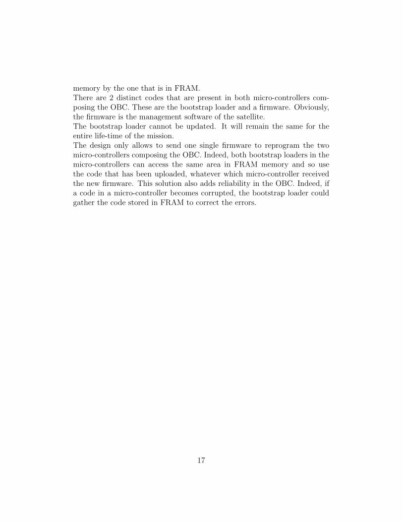
The sequence diagram on Fig. 3.1 presents the communication between theground segment and the satellite during an update procedure. This diagramrepresents a case in which there is no data loss during the packet exchanges.
If some losses occur, the ground station will not receive any acknowl-edgment indicating that the requested operation have been successfully per-formed. In this case, except for the firmware switching request, packets thatare assumed to be lost are automatically retransmitted by the ground sta-tion.One can observe in the figure that the operator first sends the file contain-ing the binary code to the satellite. When this operation is finished, hecan request to change the firmware that is executed on the powered micro-controller. The firmware change is never performed automatically when thenew firmware has been entirely received. The two reasons that motivate thisdesign choice are the following.
18
Figure 3.1: Sequence diagram of Update protocol.
First, when the firmware change is requested, the running micro-controller isrebooted to execute the bootstrap loader. Routine operations on-board thesatellite are thus suspended. Obviously, this suspension must not happenduring a critical phase of the mission. The operator must be able to deter-mine when it is most suitable to perform this switching.Second, as mentioned in section 2.6, the two micro-controllers of the OBCcan access the same area in FRAM. In case one of the two micro-controllershas already successfully uploaded a new firmware in FRAM and if the oper-ator would like to use it on the other micro-controller, it would be useless toupload the same binary representation again.
19

The diagram also highlights that firmware packets are sent one by one tothe satellite. Indeed, as the RAM memory is limited on-board, one mustensure that the packet sending neither overloads this memory nor disturbsroutine operations. Sending one packet at a time limits the risks. Moreover,this allows the ground station to easily know if each packet arrived safely atOUFTI-2.The operations performed during this protocol for sending firmware are de-scribed in detail in the following sections.
3.2 Organization of OBC
Each of the micro-controllers on the OBC board have their own flash memorywhile the same FRAM memory is accessible by both.The flash memory in each of the two micro-controllers of the OBC boardhave the same internal organization.There are three distinct zones which are defined in this memory:
• Bootstrap loader zone.
• Firmware zone.
• Information memory zone.
The three flash memory zones are each placed at fixed locations. The boot-strap loader is located at the beginning of the flash memory. The firmwareis placed just after the bootstrap loader. Obviously, a sufficient amount ofmemory is reserved for both zones to be sure that their corresponding binarycode fits in them.Information memory zone is a specific zone used to provide useful data tothe bootstrap loader. It can be modified by both the firmware and the boot-strap loader. For instance, when firmware switching is requested, the runningfirmware sets a flag in the information memory zone before rebooting. Thisflag informs the bootstrap loader that it has to switch the used firmware.The FRAM is divided in 3 main parts:
• Satellite status and measurements.
• Uploaded firmware.
• Backup firmware.
20
The satellite status and measurements are placed in the first zone. This zoneis not used for the reprogramming; only the firmware uses it.The second zone is where the firmwares sent from ground to OUFTI-2 areplaced. The bootstrap loader can copy the new firmware from this zone tothe flash memory in order to reprogram the active micro-controller.The third zone contains a backup firmware. Indeed, when the new firmwareis copied from the FRAM to the flash memory, the previous content of thelatter is cleared. But, if there is an issue with the firmware which has justbeen copied to the flash memory (such as a code integrity problem), thebackup firmware will be used to reprogram the micro-controller and avoidmajor issues in this micro-controller. The backup firmware placed in thiszone will not change during the whole mission. It is injected at this positionduring the configuration and programming of the OBC board on the ground.
3.3 Update functions in firmware
This section explains the different reprogramming operations performed bythe OBC when requested by the ground station. Their aim is to receiveproperly a new firmware, store it in FRAM, and change the firmware whichis used.For each request that the ground station can perform, and that were intro-duced in Fig. 3.1, one sub-section explains the operations that are performedin the OBC.
3.3.1 Send firmware packets
Figure 3.2 shows the operations that are performed when receiving a packetcontaining part of a new firmware.
The entire firmware is split into packets to be sent to OUFTI-2. Eachpacket contains thus a part of the firmware. A sequence number is associatedwith each of these parts. This sequence number is actually used to informthe satellite which part of the firmware it is currently receiving.This number allows to determine if a particular part of the firmware hasalready been received or not. Indeed, if the part number which is receiveddoes not correspond to the expected one, it means that the received packetprobably does not contains the expected binary code. If this happens, themicro-controller sends back a message to inform the ground station, and it
21
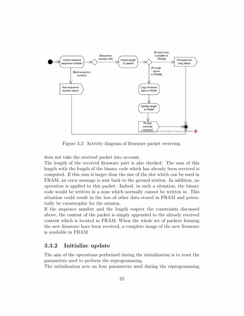
Figure 3.2: Activity diagram of firmware packet receiving.
does not take the received packet into account.The length of the received firmware part is also checked. The sum of thislength with the length of the binary code which has already been received iscomputed. If this sum is larger than the size of the slot which can be used inFRAM, an error message is sent back to the ground station. In addition, nooperation is applied to this packet. Indeed, in such a situation, the binarycode would be written in a zone which normally cannot be written in. Thissituation could result in the loss of other data stored in FRAM and poten-tially be catastrophic for the mission.If the sequence number and the length respect the constraints discussedabove, the content of the packet is simply appended to the already receivedcontent which is located in FRAM. When the whole set of packets formingthe new firmware have been received, a complete image of the new firmwareis available in FRAM.
3.3.2 Initialize update
The aim of the operations performed during the initialization is to reset theparameters used to perform the reprogramming.The initialization acts on four parameters used during the reprogramming
22

procedure:
• The expected sequence number: It is the sequence number, asdefined in the previous section, which is expected by the satellite
• The length of the firmware in FRAM: It is the length of the binarycode of the new firmware which is actually in FRAM
• Cyclic Redundancy Check (CRC) of the new firmware: It isthe CRC associated with the firmware currently in FRAM
• Not safe flag: When set, this flag signals that the firmware in FRAMis potentially corrupted and that the switch to it cannot be performed.
The three first parameters are reset.Resetting the expected sequence number variable allows to have a correspon-dence between it and the sequence number of the first packet sent from theground.As the sending of binary code of the new firmware has not been alreadystarted, the length of the firmware stored in FRAM must also be reset.Moreover, during the sending of a new firmware, this variable is also used asa counter used to know how many bytes of this new firmware have alreadybeen received. Its value is used to determine where the content of a packetcontaining the new firmware must be placed in FRAM. It is thus really im-portant to reset the value of this length variable.The CRC is also reset.Finally, the Not safe flag is set. Indeed, by definition, the new firmwarestored in FRAM is not complete during the sending. The operator shouldthus not request a switching to this incomplete firmware.
3.3.3 Send CRC
When the sending of the new firmware packets is completed, the groundstation sends the CRC that it has computed. When the micro-controllerreceives this CRC, it stores it in FRAM.The integrity of the firmware stored in FRAM is not directly checked. Thebootstrap loader is responsible for performing this operation. Indeed, in theAX.25 protocol, packet integrity is already checked. Individual parts of thefirmware contained in packets and which are stored in FRAM have thus aweak probability of being corrupted.
23
However, the integrity should also be checked when the firmware has beencopied from FRAM to flash memory. The first reason is that an error couldoccur during the transmission between FRAM and flash. The second reasonis to detect possible FRAM memory alteration between the storage and theretrieval of the firmware. The alteration can be for instance, a bit flip causedby single event upset1.A CRC computation and comparison at the end of the copy process limitthose risks.When the OBC receives this CRC, it means that the code update is finishedand that the firmware in FRAM is complete. The flag associated with thefirmware in FRAM signaling that it must not be used can thus be cleared toallow the micro-controllers to use it.
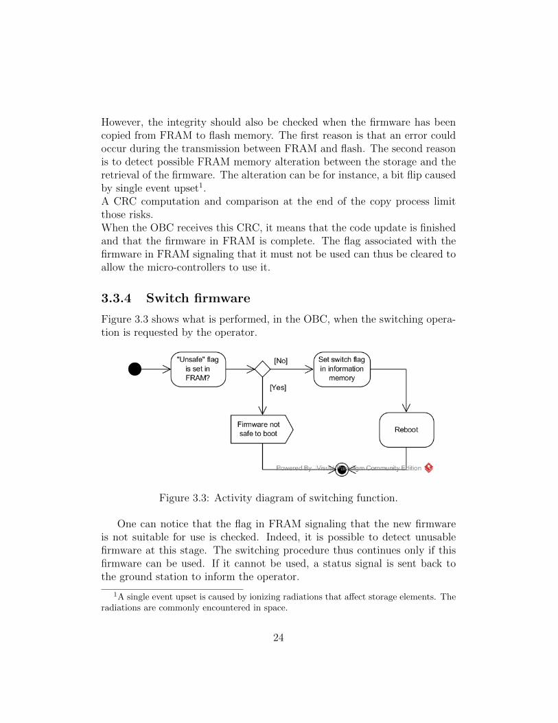
3.3.4 Switch firmware
Figure 3.3 shows what is performed, in the OBC, when the switching opera-tion is requested by the operator.
Figure 3.3: Activity diagram of switching function.
One can notice that the flag in FRAM signaling that the new firmwareis not suitable for use is checked. Indeed, it is possible to detect unusablefirmware at this stage. The switching procedure thus continues only if thisfirmware can be used. If it cannot be used, a status signal is sent back tothe ground station to inform the operator.
1A single event upset is caused by ionizing radiations that affect storage elements. Theradiations are commonly encountered in space.
24

If the firmware in FRAM can be used, the switching flag in the informa-tion memory is set. This flag is used to inform the bootstrap loader that aswitching operation must be done. Then, the micro-controller is rebooted toexecute the bootstrap loader and effectively perform the switching.
3.3.5 Check code version
The aim of this function is simply to send back the code version to the groundstation when requested by the operator. It allows the operator to know whichcode is currently executed on the micro-controller, and also to determine ifan update procedure succeeded or not.For instance, if the backup firmware is the version 0 of the firmware, that thefirmware currently executed on the micro-controller has version numbered1.0, and the operator sends the version 2.0 of the firmware. If at the end ofthe whole update procedure, the firmware executed on the micro-controllerhas version number 2.0, it means that the update succeeded. But if themicro-controller executes the version 0, it means that a problem occurred.Obviously, the version number associated with a new firmware must be up-dated when preparing the sending of this new firmware. Otherwise it wouldbe impossible to distinguish two different firmwares.
3.4 Bootstrap loader
Figure 3.4 shows the operations performed by the bootstrap loader.The bootstrap loader is executed each time the micro-controller is re-
booted. As reboot does not exclusively occur when a firmware switch isrequested, the bootstrap loader must always check if a firmware change isnecessary or not. If it is not requested, the bootstrap loader simply boots onthe firmware located in the flash memory and does not do any modificationto the running firmware.If a firmware switch is requested, the bootstrap loader performs the copyoperations and integrity checking like presented in Fig. 3.4.One can observe that, if the integrity of the uploaded firmware is compro-mised at the end the copy operation, the flag signaling that the firmware isnot suitable for use is set. Indeed, the error source cannot be determined.It could be a copy issue or an FRAM memory alteration. The choice of nottaking any risks has been chosen, and the ”not safe” flag is set in FRAM.
25
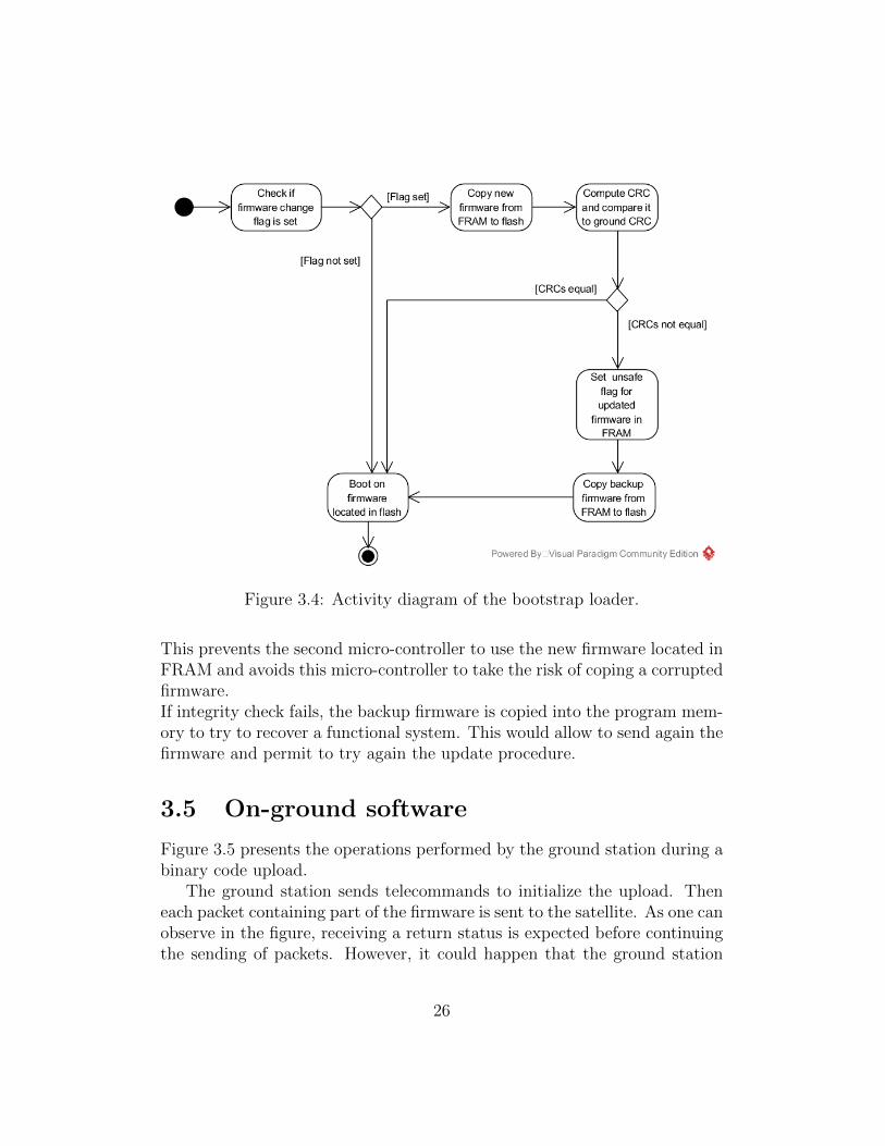
Figure 3.4: Activity diagram of the bootstrap loader.
This prevents the second micro-controller to use the new firmware located inFRAM and avoids this micro-controller to take the risk of coping a corruptedfirmware.If integrity check fails, the backup firmware is copied into the program mem-ory to try to recover a functional system. This would allow to send again thefirmware and permit to try again the update procedure.
3.5 On-ground software
Figure 3.5 presents the operations performed by the ground station during abinary code upload.
The ground station sends telecommands to initialize the upload. Theneach packet containing part of the firmware is sent to the satellite. As one canobserve in the figure, receiving a return status is expected before continuingthe sending of packets. However, it could happen that the ground station
26

Figure 3.5: activity diagram of ground segment packet sending
never receives this return status. For instance, because the satellite does notreceives the packet or drops it2. To take this case into account, a timer isalso set when the packet is sent. If no status is received by the end of thistimer, the packet is considered lost and is resent.Three type of status can be received from the satellite when sending packetscontaining part of the firmware:
• Packet correctly received.
• Bad sequence number.
• Firmware too long.
When a packet containing part of the firmware is correctly received, thesending operation simply continues.If a bad sequence number status is received, the operator is warned andthe sequence number which was expected by the satellite is checked. If thisexpected sequence number is greater then the one sent with the previouspacket, it probably means that the packet was already received by the OBCbut that the corresponding acknowledgment was not received by the groundstation. The sending simply continues with the next packet.
2Because the packet integrity check fails.
27

Finally if a firmware too long status is received, the ground station stops tosend packets containing part of the firmware. In fact, continuing sending thepackets would be useless as the satellite would not be able to store contentof those packets properly in FRAM.
28

Chapter 4
Implementation details
The aim of this chapter is to explain the details of implementation. Sections1 and 2 present the micro-controllers, the memories used, and the way thememory elements are organized. Section 3 focuses on the bootstrap loaderimplementation. Section 4 gives details about particular protocols used toupdate the OBCs of OUFTI-2. Section 5 details the telecommands andtelemetries implemented to allow the OBC update. Section 6 discusses themechanism used to ensure integrity of the firmware. Section 7 presents themodifications made to the ground station software. Section 8 exposes a typeof file that is used by the linker and that must be modified for the purposeof reprogramming. Section 9 presents the procedure that must be followedto perform a reprogramming of the OBC. The initialization procedure usedto program the micro-controllers on the ground is presented in section 10.
4.1 Flash memory
The micro-controllers that compose the OBC board are manufactured byTexas Instruments. They are MSP430f1611. In this section, the first partexplains the organization of the flash memory, and the second explains howthe different applicable operations are performed on it.
4.1.1 Flash memory organization
In the micro-controllers, the binary code is placed in flash memory and isdirectly executed from this location. Three particular zones are defined in it:
29

Code memory: This memory zone contains the code1 developed by theuser. Its size is about 48KB.
Interrupt vector: This memory zone contains the addresses of the inter-rupt routines that must be executed when an interrupt request occurs.Its size is 32 bytes.
Information memory: This is a memory zone that can contain code ordata. Its size is 256 bytes.
The code memory is divided into 512 bytes segments, and the interruptvector is located in the last segment of this memory zone.The information memory is organized into 2 segments of 128 bytes.The micro-controllers also contains RAM memory that can be used duringthe code execution. There is about 10 KB of it accessible in the micro-controller used.The memory space organization is presented on Fig. 4.1. The exact locationsreserved for the bootstrap loader and the firmware, discussed in section 3.2,are also highlight in the figure.
Figure 4.1: Memory organization of MSP430f1611.
1But it can also contains data.
30

As discussed in section 3.2, a flag is set if the bootstrap loader has toperform a firmware switching operation. This flag is located at the address0x1082 in information memory. The bootstrap loader also has to know whichis the address of the first instruction of the firmware. This is located ininformation memory at address 0x1080.The interrupt mechanism is not used in the bootstrap loader, the interruptvector must thus be the one that is associated with the firmware used in flashmemory. However, on the MSP430 architecture, the reset vector is located atthe address 0xFFFE in the interrupt vector zone, and contains the addressof the instruction that must be executed after a reboot. This reset vector, inthis work, must thus point to the first instruction of the bootstrap loader.
4.1.2 Operation applicable on flash memory
Three basic operations can be applied to the flash memory: read, erase, andwrite.Read mode is the one which is enabled by default. Access to the content canbe performed either by byte or by word of 16 bits.Before writing new content to an address, because of the characteristics ofthe flash memory, the previous content must be erased. However, a singleaddress cannot be erased alone. Erase operation can be performed eitheron one single segment or on the entire memory except for the informationmemory, or on the entire memory. It could thus be necessary to save databefore erasing. Indeed, erasing the content of one address would require toerase at least one segment. If the data contained in the rest of the segmentshould not be modified, restoring them would be necessary at the end of theerase operation.The write operation can be performed per byte, per word of 16 bits, or perblock of 64 bits. Writing more bits in a single write operation allows to speedup the writing process.The flash memory has an integrated controller that controls write and eraseoperations. During the operations, the controller takes the control of theflash, and the CPU cannot read it anymore. As the program is stored inflash, the CPU is put in idle mode until the erase or write operation is fin-ished. When the flash is accessible again, the CPU simply continues theexecution from where it was stopped. However, if the CPU must absolutelycontinue the execution, the code could be executed from RAM.It is worth to mention that it is possible to erase the segment containing the
31

next instruction that must be executed by the CPU. This should obviouslybe avoided as this would result in undetermined behavior in the subsequentexecution.Before write and erase, all interrupts should be disabled. Indeed, the inter-rupt vector is not accessible as it is located in flash.In this work, the erase operation is performed by segment. It is the bestmethod as the bootstrap loader is also located in flash memory. Using oneof the two other erase methods could lead to loose the bootstrap loader orto add additional computations to save and restore it.The reading and writing operation are performed per byte. This was chosenbecause the operations performed on the FRAM memory presented in thenext section are also done per byte.Finally, three registers are used to configure the integrated controller of theflash memory. Their names are FCTL1, FCTL2, and FCTL3. In order to switchbetween the different modes, only FCTL1 and FCTL2 values must be modified.The value corresponding to the different modes are presented in Table 4.1.Details about the choices of those values can be found in [16].
FCTL1 FCTL3Read 0x0A500 0x0A510Erase 0x0A502 0x0A500Write 0x0A540 0x0A500
Table 4.1: Register values of the flash memory controller.
4.2 FRAM Memory
The used FRAM memory on the OBC board has a capacity of 2 Mbitsand is manufactured by Cypress Semiconductor. The first part gives detailsabout the chosen memory organization. The second part discusses the SerialPeripheral Interface (SPI) bus, which is used by the micro-controller and theFRAM to communicate.
4.2.1 FRAM memory organization
The addresses ranges allocated to the different FRAM zones defined in sec-tion 3.2 are presented in Fig.4.2. Despite the fact that a firmware code could
32

take up to 46 KB according to flash memory division, the choice to allocateonly 32KB for each firmware in FRAM was made. The firmware size couldthus not be greater than 32 KB. The reason for this is to keep as much spaceas possible for the logs and measurements stored in it. Moreover, at the timeof writing this document, size of the firmware was about 30 KB. A 2 KBmargin is thus available for code size variation during update.However, if the firmware must be modified later during the satellite develop-ment and this space is judged to be too small, it can easily be enlarged tofit the size of the new code. But it would obviously reduce the size availablefor logs and measurements.The backup binary code is not modified during the mission. When this codeis stored in FRAM on the ground before the mission, it will no longer bepossible to change it. One can imagine to reduce the size of backup firmwarezone to have exactly the space needed for this backup firmware, and enlargethe updated firmware zone with the freed space. This would thus provide abetter size variation margin for the updated codes.Figure 4.2 also shows that 2 fields are marked as unused in the backupfirmware zone. The reason for this is to allow the bootstrap loader to treatupdated and backup firmware in the same way. The bootstrap loader justignores values of those fields when using the backup firmware.The firmwares are stored linearly in the FRAM. This means that if thefirmware in FRAM has a length N , the N − 32 bytes stored in FRAM cor-respond to the binary code and that the last 32 bytes are the correspondinginterrupt vector.
4.2.2 SPI bus
Data are sent to and received from FRAM by using an SPI bus.It is a serial master-slave communication type. On a given bus there is onlyone device acting as master but multiple slaves can be present on it. TheSPI bus is a full-duplex one, and it uses 4 signals in order to transmit databetween the devices:
• CS: Chip select
• SO: Serial Output, also called Master in Slave out (MISO)
• SI: Serial Input, also called Master out Slave in (MOSI)
33

Figure 4.2: Organization of FRAM Memory.
• SCK: Serial Clock.
Typically, all slaves share the same MISO, MOSI, and SCK physical links. Themaster thus uses the same wires to communicate with all slaves. However,all the slaves have their dedicated chip select link to the micro-controller.The communication is always initiated by the master and the slaves justrespond to its requests. The slave never starts a communication by itself.When starting a communication, the master begins by generating a clocksignal on the SCK link. Then, it puts the CS link associated with the slavelow. At that moment, the data transmission can be started using the MISO
and MOSI links. At the end of the communication, the master puts the CShigh and stops sending the clock signal.Bits are sent one by one through the links, and the most significant bit isalways sent first. The clock signal is used to synchronize the communications.The devices read their input link at either the raising edge or the falling edgeof the clock signal. The signals sent and received must thus follow this timingto be correctly transmitted between two devices.In this work, the master of the bus is one of the micro-controllers and theslave is the FRAM device. The micro-controllers have dedicated pins thatare used to perform SPI communication and they are thus used. The FRAMsamples data at the rising edge of the clock.The action the FRAM has to execute is transmitted using an opcode. The8 first bits of the communication must always be this opcode.
34

The way the data transmission must be performed to execute a read operationis presented in Fig. 4.3. On the input line of the FRAM the opcode is firsttransmitted. Then, the 18 bits forming the address that must be read aresent. Finally the FRAM transmits the content located at this address on itsoutput link.
Figure 4.3: Read operation on FRAM [5].
By default write operation are locked on the FRAM. Before performingany write operation in FRAM, the operation must be unlocked. This isperformed by sending the WREN opcode.The signals that must be sent to perform a write operation are shown onFig. 4.4. The opcode, followed by the 18 bits address where data mustbe written are transmitted by one micro-controller on the input line of theFRAM. Finally the 8 bits of data are sent on the same link.
Figure 4.4: Write operation on FRAM [5].
The values of the different opcodes that are used in this work are presentedin table 4.2.
35

OpcodeRead 0b00000011Write 0b00000010
WREN 0b00000110
Table 4.2: FRAM opcodes.
4.3 Bootstrap loader
The bootstrap loader is coded in C language. It is called each time the micro-controllers are turned on. It first checks the content of the address 0x1082in flash memory to know if a firmware change is needed.If the update is not requested, it only creates a function pointer to the addresscontained at position 0x1080 in information memory and calls this function.The effect is thus to boot the firmware located in flash memory.However, if the firmware must be changed, the copy from FRAM to flashmemory is performed before creating the function pointer.The copy is performed byte per byte from FRAM to flash. There is onevariable used to know which address must be read in FRAM, and one pointerused to know where the data must be placed in flash memory. The flashmemory pointer always points initially to address 0x4A00, and the initialaddress in FRAM is either 0x2EE00 when using the backup firmware or0x36AFF when it is an updated firmware that is copied.The copy is performed in two phases. During phase 1, all the firmware exceptthe interrupt vector is copied. Phase 2 is about the interrupt vector update.The operations performed during phase 1 are presented in Fig. 4.5. Eachtime 512 bytes have been copied, a flash segment erase is performed. Indeed,at that moment, the flash pointer enters in a new segment which must beerased before being rewritten.When phase 1 is finished, phase 2 starts to complete to firmware copy. Inthis phase, the following actions are performed:
1. Save the content of the reset vector.
2. Move the flash pointer to the beginning of the interrupt vector in flashand erase the corresponding segment.
3. Copy 30 bytes and increment flash pointer and FRAM address.
4. Restore the saved reset vector.
36
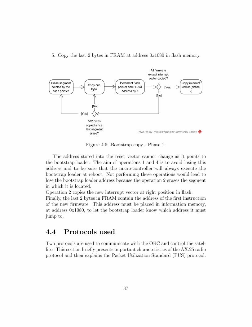
5. Copy the last 2 bytes in FRAM at address 0x1080 in flash memory.
Figure 4.5: Bootstrap copy - Phase 1.
The address stored into the reset vector cannot change as it points tothe bootstrap loader. The aim of operations 1 and 4 is to avoid losing thisaddress and to be sure that the micro-controller will always execute thebootstrap loader at reboot. Not performing these operations would lead tolose the bootstrap loader address because the operation 2 erases the segmentin which it is located.Operation 2 copies the new interrupt vector at right position in flash.Finally, the last 2 bytes in FRAM contain the address of the first instructionof the new firmware. This address must be placed in information memory,at address 0x1080, to let the bootstrap loader know which address it mustjump to.
4.4 Protocols used
Two protocols are used to communicate with the OBC and control the satel-lite. This section briefly presents important characteristics of the AX.25 radioprotocol and then explains the Packet Utilization Standard (PUS) protocol.
37

4.4.1 AX.25 protocol
The AX.25 data link layer protocol is used to transmit control packets be-tween the ground station and the satellite. The control packets are presentedin detail in the section 4.4.2.The AX.25 frame structure used for OUFTI-2 mission is presented in Table4.3.
Flag Address Control PID Data CRC Flag1 byte 14 bytes 1 byte 1 byte Max. 256 bytes 2 bytes 1 byte
Table 4.3: AX.25 frame structure for OUFTI-2.
All the fields of this structure will not be explained in detail here. Indeed,the decoding of the frames is not part of this work. However, it is importantto notice that a maximum of 256 bytes of data can be transmitted in a singleAX.25 frame. A particular care must thus be taken not to exceed this sizewhen sending a new firmware.The CRC field in the AX.25 frame is used to check the integrity of this frame.This CRC is completely independent from the one used to check the integrityof the entire firmware.
4.4.2 PUS protocol
The PUS protocol is a norm written by the European Space Agency (ESA).It defines the way communications between the ground station and the satel-lite should be performed. The communications are performed using packetscalled telecommands and telemetries. Telecommands are the packets sentfrom the ground to the satellite. They are used to request the OBC to per-form some operations. Telemetries are the packets sent from the satellite tothe ground station. They are used to send parameters and operational statusto the ground.Packets headers are defined for telecommands and telemetries. The decodingof the headers is not part of this work. Indeed, the OBC firmware is responsi-ble for performing this decoding for all type of telecommands and telemetriesused for the OUFTI-2 mission. The reprogramming packets disencapsulationis also performed by it. Details about the PUS headers will not be presentedin this work, but can be found in [2].However, two particular fields in the headers are meaningful for this work.
38

These are the type and sub-type fields. Telecommands and telemetries aregrouped together depending on their utilization and are thus classified bytype. The sub-type is used to define a function that can be implemented ina given type. These fields are thus used to identify the telecommands andtelemetries and to allow their proper treatment.The types numbered from 0 to 127 are reserved by the norm. However,mission specific types can be defined, but they must be numbered between128 and 255. As no type and sub-types were defined for the reprogrammingcapability, it has been chosen to define new functions. Type 128 has beenallocated for reprogramming functions, and sub-types 1 to 5 are used in thistype. Section 4.5 exposes the allocations of these sub-types numbers to thedifferent functions.Obviously, some data payloads can be placed in the PUS packets to exchangeinformation with the satellite. For telecommands, the size of the PUS headeris 9 bytes. One should take into account the fact that the maximum alloweddata size in AX.25 frames cannot be exceeded, particularly during the send-ing of the new firmware data.The PUS frames are encapsulated in the data fields of AX.25 frames andthen sent by radio signals.
4.5 Telecommands and telemetries
This section presents the telecommands and telemetries that are used toperform the reprogramming procedure. For each of them, the PUS type andsub-type used for telecommands and telemetries are presented.The data structures used for each telecommand and telemetry are also de-scribed.
4.5.1 Initialize update
The PUS type of telecommands and telemetries associated with this functionis 128. The sub-type has value 1.When receiving this type of telecommand, the satellite performs the opera-tions described in section 3.3.2. As the operation resets some parameters usedduring the reprogramming procedure, no additional information is needed.The telecommand is an empty PUS packet.Data that is placed in the telemetries is a single byte used to return a status
39

to the ground. No particular error could occur during this initialization. Theonly status code that can be returned to ground in the telemetry is 0, and itsignals that the operation has been properly performed. Not receiving thisstatus would mean that the telecommand has not been received by the satel-lite, or that the telemetry did not arrived properly to the ground station. Itcould also mean that the satellite or the ground station dropped the packetdue to issues in it (e.g. bad AX.25 CRC). But, whatever the reason thatlead to this situation, the telecommand packet should be sent again by theground station.
4.5.2 Firmware sending
The PUS type of telecommands and telemetries associated with this functionis 128. The sub-type has value 2.Upon receiving this type of telecommand, the OBC executes the operationsthat are presented in section 3.3.1.Obviously, as the aim of the telecommands is to send the new binary codeto the OBC, data must be sent in them. The way data is organized in thetelecommand packets is presented in table 4.4.
Sequence Number Length Binary code1 byte 1 byte Max. 245 bytes
Table 4.4: Organization of PUS telecommand for the sending of the firmware.
The size of the binary code per packet cannot exceed 245 bytes. Thischoice has been made to conform to the fact that AX.25 data field must nothave a size that is greater than 256 bytes. Indeed, having 247 bytes of datain the PUS frame in addition to the 9 bytes of header leads to reach the limit.The sequence number is the part number of the firmware. It is representedby using a single byte. This size allows to have 256 different values, which issufficient. In fact, as the firmware size must not exceed 32KB, the sendingcan be performed by using 131 telecommands and the sending thus uses 131different values for the sequence number field.Similarly, the field representing the length of the binary code is 1 byte long.Indeed, as the binary code in packet must not exceed 245 bytes, 1 byte issufficient to represent this length.The format used for the telemetries is presented in Table 4.5. The statusfield can take 3 different values:
40

• 0: means that the firmware part has been well written in FRAM
• 1: means that the packet received has not the expected sequence num-ber
• 2: means that the firmware is too long and that it cannot be stored inFRAM
Status Sequence Number1 byte 1 byte
Table 4.5: Organization of PUS telemetry for the sending of the firmware.
For the telemetries, the meaning of the value stored in the sequence num-ber field is dependent on the value in the status field.If the status is 0, this value is the sequence number of the packet that hasjust been received that is stored in this field. This thus allows the groundstation to know which sent packet it is receiving an acknowledgment for.If the status is 1, the value of sequence number that the OBC expects nextis returned in this field.Finally, if the value of the status is 2, the sequence number field is simplynot used. It should thus be filled with 0.With the returned values, the necessary sequence number checking, explainedin section 3.5, is possible.
4.5.3 CRC sending
The PUS type of telecommands and telemetries associated with this functionis 128. The sub-type has value 3.The only data that is sent using the telecommand is obviously the CRC.There is only this 2 bytes of data in the PUS telecommand packet.In the associated PUS telemetry, there is only one byte of data that representsa status. It can only take the value 0, which signals that the operation hasbeen correctly performed. Indeed, when receiving the CRC, the OBC juststores it in FRAM. No particular problem could thus be reported.If the telemetry is not received after the sending of the CRC, this could meanthat the telemetry has not been received properly by the ground station orthat the telecommand has not been received correctly by the satellite. Thetelecommand should thus be resent.
41

4.5.4 Switch between the firmwares
The PUS type of telecommands and telemetries associated with this functionis 128. The sub-type has value 4.When requesting a firmware change, there is no additional data to send withthe request. Indeed, the OBC reboots to execute the bootstrap loader. Thedata field of the PUS telecommand is thus empty.There is only one byte data in the telemetry that is sent to the ground station.The data is as usual a status. It can take two values:
• 0: means that the switching has started
• 1: means that the firmware in FRAM is not suitable for use (see section3.3.4)
Obviously, if no status is received, the operator should send the telecommandto the satellite again.
4.5.5 Code version checking
The PUS type of telecommands and telemetries associated with this functionis 128. The sub-type has value 5.When receiving this request, the OBC must just send back the version of thecode that is currently being executed on the powered micro-controller. Nodata must thus be encapsulated in the request. The data field is kept empty.The telemetry is used to send back the version number. The data encapsu-lated in this telemetry is a single byte containing the version number. Onebyte is sufficient to represent this version number. In principle, the repro-gramming capability should rarely be used, it is thus not expected to have256 different firmware versions.As with the other functions, if no response is got after some time, it probablymeans that either the telecommand or the telemetry has not been receivedcorrectly or dropped. The telecommand should thus be resent.
4.6 Reliability, computation of CRC
This section presents the way the firmware binary code storage and transferreliability has been addressed. The first part explains the theory behind the
42

CRC, and the second one explains the way it has been implemented in thiswork.
4.6.1 Theory about the CRC
Cyclic Redundancy Check (CRC) is a method that is used to ensure that nobit errors such as bit flips occurred in a sequence of bits. That is a methodwhich improves reliability in data storage and transmission.A polynomial is fully defined by its set of coefficients. A sequence of bitscould be seen as a polynomial. For instance, the sequence of bits 1011 canbe represented by the polynomial 1x3 + 0x2 + 1x + 1.The CRC method can be explained in terms of polynomials. Let us call M(x)the polynomial representing the message to protect, and G(x) an arbitrarypolynomial of degree r called the generator. A new polynomial can be definedby their multiplication:
T (x) = M(x) ·G(x)
The obtained polynomial T (x) thus has a degree augmented by r comparedto the polynomial M(x). The polynomial T (x) can be transformed to:
T (x) = M(x) · xr + R(x)
where R(x) is the remainder of M(x)·xr
G(x). This polynomial R(x) forms the
CRC, and T (x) is the polynomial representation of the encoded data, thatare sent.When receiving the polynomial T (x), two methods can be used to checkwhether problems occurred during transmission.The first method is to check that it is divisible by G(x). If it is the case, itprobably means that no data alteration occurred. If not, it is certain thatthere is an issue with the received polynomial representation.The second method is to recompute R(x) on the extracted message and checkthat the computed result correspond to the received one. If they are equal,it is assumed that no problem occurred. If they are not equal, it means thatsomething unexpected happened.The choice of the generator polynomial impacts the results and the way dataare protected, but some polynomials are widely used and are known to givegood results.
43
4.6.2 Implementation of the CRC
On this work, as in many applications, a 16 bits CRC is used. The algorithmused is based on the firmware polynomial division by a fixed generator poly-nomial to obtain the rest of this division.The chosen generator polynomial is the CRC-CCITT and the algorithmtreats all bits of the firmware one by one and works as follows:
1. Initialize a CRC variable to value 0xFFFF.
2. Shift left the CRC variable and insert the left most remaining bit ofthe message at the position of the bit freed in the CRC variable.
3. If the bit shifted out of the CRC was set (i.e 1), apply XOR operationbetween the CRC variable and the generator polynomial to obtain thenew value of CRC variable.
4. Repeat operation 2 and 3 while all bits of the messages have not beentreated.
This algorithm is applied in both the ground station and the satellite, andone checks whether the two CRC values obtained are equal.
4.7 Ground station software modifications
The ground software, developed in Java language, and which was used forOUFTI-1 mission was adapted to use for communication with OUFTI-2. Inthis work, the five types of telecommands and telemetries used for repro-gramming procedure have thus been added in this ground station software.Obviously, mechanisms for sending telecommands and receiving telemetrieswere already implemented and were reused for reprogramming functions.However, by contrast with the other telecommands, new threads are instan-tiated for sending reprogramming telecommands. Indeed, their usage allowsto send packets one after the other, and to deal with retransmission in caseof communication issues (such AX.25 packet dropped by the satellite dueto integrity problems). This retransmission mechanism is implemented forthe following three telecommands: the initialization of reprogramming, thesending of the firmware, and the sending of the CRC. For the three telecom-mands, the operator cannot request the sending of a particular one as packets
44

are sent sequentially. An automatic retransmission mechanism is thus nec-essary. The retransmission mechanism is not implemented for the two othertelecommands because, in case of communication issues, the operator cansimply manually request the resending of the telecommand.The retransmission mechanism works as follow: when a telecommand is sent,a new thread is instantiated and it waits to get the corresponding acknowl-edgment telemetry from the satellite. When it receives it, the thread is wakenup to send the next telecommand. However, if the telemetry is not receivedby the ground station within 5 seconds, the ground station will consider thata problem occurred. The thread is thus waken up to resend the packet thatis presumed to be lost.Two new Java classes have been added to the ground software. The first oneis called Page. It is used to store data that are sent in a single packet. Thesecond is called FileSender, and it is responsible for extracting binary codefrom the file and manages the sending of it to the satellite. The files thatare used are Intel Hex files and the binary codes of the firmwares are storedin them. More details about those files are presented in the Appendix A.The first operation that is performed by the FileSender when it is instan-tiated is to read the Hex file and to break data into packets. The packetsare organized using the Page class. At the end of the reading, a set of Pageobjects are obtained and the sending procedure can start.During the sending of a firmware, the FileSender class decides which arethe data to send to the satellite. Based on the received acknowledgments,this class thus determines the packet that must be sent. This class decideswhether a packet containing part of the firmware must be resent or not.
4.8 Linker command file
When the source code is compiled, object files are obtained. They mustbe linked together to obtain the binary code that can be executed by themicro-controllers. The linker performs this action. It is also responsible fororganizing the address space and for preparing the binary code to be placedat appropriate position in the flash memory.With the linker used with Code Composer Studio2, this memory organiza-tion is defined in a linker configuration file. The content of this file can be
2Code Composer Studio is the Integrated Development Environment (IDE) used todevelop embedded application for Texas instrument micro-controllers.
45

modified to obtain the desired configuration, and is changed to get the orga-nization presented in section 4.1.1.The command file contains MEMORY and SECTIONS directives. The aim of theMEMORY directive is to assign names to ranges of memory.The SECTIONS directive is used to create output sections using input sec-tions coming from object files, and allocate the output sections to the micro-controllers memories. The allocation is performed using the names definedin MEMORY directive.In this work, only the MEMORY directive is changed to tune the memory orga-nization. The default configuration for the MSP430f1611 micro-controller ispresented on Listing 4.1.
MEMORY{
SFR : o r i g i n = 0x0000 , l ength = 0x0010PERIPHERALS 8BIT : o r i g i n = 0x0010 , l ength = 0x00F0PERIPHERALS 16BIT : o r i g i n = 0x0100 , l ength = 0x0100RAM : o r i g i n = 0x1100 , l ength = 0x2800INFOA : o r i g i n = 0x1080 , l ength = 0x0080INFOB : o r i g i n = 0x1000 , l ength = 0x0080FLASH : o r i g i n = 0x4000 , l ength = 0xBEE0INT00 : o r i g i n = 0xFFE0 , l ength = 0x0002INT01 : o r i g i n = 0xFFE2 , l ength = 0x0002INT02 : o r i g i n = 0xFFE4 , l ength = 0x0002INT03 : o r i g i n = 0xFFE6 , l ength = 0x0002INT04 : o r i g i n = 0xFFE8 , l ength = 0x0002INT05 : o r i g i n = 0xFFEA, l ength = 0x0002INT06 : o r i g i n = 0xFFEC, l ength = 0x0002INT07 : o r i g i n = 0xFFEE, l ength = 0x0002INT08 : o r i g i n = 0xFFF0 , l ength = 0x0002INT09 : o r i g i n = 0xFFF2 , l ength = 0x0002INT10 : o r i g i n = 0xFFF4 , l ength = 0x0002INT11 : o r i g i n = 0xFFF6 , l ength = 0x0002INT12 : o r i g i n = 0xFFF8 , l ength = 0x0002INT13 : o r i g i n = 0xFFFA, l ength = 0x0002INT14 : o r i g i n = 0xFFFC, l ength = 0x0002RESET : o r i g i n = 0xFFFE, l ength = 0x0002
}
Listing 4.1: MEMORY directive in linker command file.
46

One can observe that ranges of addresses are associated with names.By modifying origin addresses and length, it is thus possible to change thememory organization. In particular, for the purpose of reprogramming, theFLASH, RESET, and INFOA ranges are modified.
4.9 Reprogramming procedure
This section describes the procedure that must be followed to correctly per-form the reprogramming of the OBC. The following operations must be per-formed sequentially by the ground station operator:
1. Ensure that the compiler is in Release mode.
2. Enable Hex File generation.
3. Change firmware version number in file definition.h.
4. Check that the MEMORY directive in the linker command file has theappropriate form.
5. Compile and link the new firmware.
6. Select SOFTWARE_UPDATE command in the ground station software.
7. In the parameters zone, select the Hex File that must be sent.
8. Start the sending by pushing Send TC button in the ground stationsoftware.
9. Wait for the end of the sending of the packets and CRC.
10. In the ground station software , select the command SWITCH_FIRMWARE
and send it using Send TC button.
11. Wait 3 minutes.
12. In the ground station software, select the command GET_FW_VERSION
and send it using Send TC button.
13. Check the version running on the satellite.
47

The way to perform step 2 is presented in Appendix B. Step 3 must beperformed to have a unique version number for the code that will be sentto the satellite. This will allow, at step 13, to exactly know whether thenew code is actually executed on the OBC. Step 4 permits to be certain thatthe memory map for the code that will be linked is correct. Indeed, havinga bad memory map could lead to obtain a code that is not executable atthe position where it will be located in the micro-controller in the satellite.Listing D.1 in Appendix D describes the MEMORY directive that must be used.Step 6 to 10 corresponds to the sending of telecommands that contain thenew firmware. At step 11 one must wait for three minutes before going tothe next operation. Indeed, the bootstrap loader on-board the satellite takesabout 2 minutes and 30 seconds to retrieve the new firmware from FRAM,store it in flash, and compute the CRC. The aim of the two last operationsis to check that the executed firmware has the expected version number. Ifthis is not the case, this means that a problem occurred during the update.
4.10 Initialization procedure
This section presents the procedure that must be followed to initialize theOBC on-ground. It is divided in two parts. The first deals with the storageof the backup firmware in the FRAM, and the second deals with the micro-controllers initialization.For the first part, the operations that must be performed are the following:
1. In the file update.h, change the defined UPDATE_FW_FRAM value. Thenew address must be 0x2EE00.
2. Modify the linker command file such that the MEMORY directive is theone presented in Listing D.1 in Appendix D.
3. Compile, link, and program one of the OBC micro-controller with thiscode.
4. In the file update.h reset the define UPDATE_FW_FRAM value to 0x36AFF.
5. Apply the first 9 operations of the procedure presented in section 4.9.
The first step is used to change the address where the received firmware isstored; the received firmware is placed in the backup zone in the FRAM. Step
48

2 and 3 ensure that an executable code is stored in the micro-controller. Step4 restores the address such that the backup firmware that will be generated atstep 5 contains the right address. Finally, during step 5, the backup firmwareis sent and stored at the right position in FRAM.At the end of this first part, the final micro-controllers initialization can start.For both micro-controllers on the OBC board, the following operations mustbe performed:
1. Modify the linker command file of the bootstrap loader to obtain theconfiguration presented in Listing D.3 in Appendix D.
2. Modify the linker command file of the firmware to obtain the configu-ration presented in Listing D.2 in Appendix D.
3. Make the configuration such that the entire flash is not erased whenthe firmware programming will be performed.
4. Compile, link, and program the micro-controller with the bootstraploader.
5. Compile, link, and program the micro-controller with the firmware.
Step 1 and 2 ensure that the bootstrap loader and the firmware willbe placed at the right position in flash memory. The default configura-tion is erasing the entire flash before programming it. However, as it canbe seen with step 4 and 5, the bootstrap loader is first programmed andthen the firmware is. However, when the firmware is programmed, thebootstrap loader must not be erased. The aim of step 3 is to ensure thebootstrap loader will not be erased. The configuration made in step 3, forCode Composer Studio IDE, is presented in Appendix C.
49

Chapter 5
Tests
This chapter describes the procedures and results of tests used to check thatthe reprogramming capability is working. Section 1 describes the tests thatwere performed using only the flash memory. Section 2 describes the testsperformed when the FRAM memory has been added in the system. Section3 presents the tests which that were done after the integration of the solutionin the OBC firmware. Finally, section 4 describes tests performed check thesending of a new firmware via radio signals.
5.1 Flash memory based
This section describes tests that were performed on a simplified hardwaresystem using a single micro-controller.
5.1.1 Configuration
An MSP430f1612 micro-controller was used to perform the tests. It is similarto the MSP430f1611 that is used on the OBC board. The only differences isthat it has a little more flash memory (55KB vs 48KB) but less RAM (5KBvs 10KB).For this part of the tests, a simple firmware was developed. Its aim wasonly to receive a new firmware code and store it at another location in flashmemory. At this stage, the AX.25 and PUS protocols were not alreadyused and only the data structures presented in section 4.5, without the PUSheader, were transmitted by using a serial port.
50

A simple Java program was written to send bytes of data through the serialport and to send them to the micro-controller. This program implementationwas a first sketch of the solution integrated in the ground station software.The protocol used for send the new firmware was the same as the one usedin the final implementation.The bootstrap loader had limited responsibility at that time. It had only tocheck which firmware it had to boot on and choose the appropriate addressto which it had to jump in consequence. The only copies that the bootstraploader had to perform concerned the particular case of the interrupt vectors.Indeed, the interrupt vectors associated with the firmware must be copied tothe right location in the flash memory. The CRC was not yet implementedin the bootstrap loader; it was checked before rebooting when the switchingrequest was performed. If the CRC was not correct, the firmware change wassimply not performed.The code memory was thus divided in three zones: the bootstrap loader zone,the zone for firmware 1, and the zone for firmware 2.
5.1.2 Objectives
The aims of the tests performed in this section were multiple:
• Test the write and erase operations performed on flash memory.
• Test the bootstrap loader switching capability.
• Test the CRC computation and checking.
• Check that the retransmission mechanism in the sending procedure wasworking.
The objectives were to check that storing a new firmware in another locationin flash memory and that safely booting on it was feasible.
5.1.3 Procedures
Three test procedures were used in this section.In the first procedure, the sending protocol was applied and the new firmwarewas stored in the zone for firmware 2 in flash memory. The new firmwaremust be executable from this location. The correct CRC was sent, then,when the switching between the firmware was requested, the new firmware
51

should thus be executed from its location in flash.The second procedure was similar to the first, excepting that an incorrectCRC was sent to the micro-controller at the end of the sending procedure.The switching between the firmware should not be executed in this case.Checking whether the executed firmware has changed was performed exactlyas in the final version. The code version number defined in the code waschecked.The third procedure tested the retransmission mechanism. The micro-controllerwas configured to drop some packets that it had received. The Java programthat sends the packets thus had to resend them. In the Java program, logsdisplayed information about the sent packets. Checking those logs allowedto determine if dropped packet were effectively retransmitted.
5.1.4 Results
The procedures were applied multiple times and all the objectives of the testswere fulfilled. All the functions developed were operating correctly.In particular, the switching between the firmwares occurred correctly whenthe CRC associated with the new firmware was correct. By contrast, theswitching was not performed when the CRC was not the appropriate one.Packets that were dropped during executions of the third procedure were cor-rectly retransmitted, and in each case, the switching between the firmwareswas possible at the end of the sending protocol.
5.2 FRAM memory based
This section describes the tests that where performed when the FRAM mem-ory was added to the system.
5.2.1 Configuration
As for the flash memory based tests, the present tests were performed usingthe MSP430f1612 micro-controller. However, an external flash memory wasconnected to the micro-controller. As on the final OBC board, the commu-nication with this FRAM memory was performed by using a SPI bus.The simple firmware developed for tests in section 5.1 was reused, but adapted
52
to communicate correctly with the FRAM. In particular three of the five re-programming functions of the OBC were adapted:
• The function executed when receiving a packet containing a part of thenew firmware.
• The function executed when receiving the CRC associated with thenew firmware.
• The function executed when the operator requests a switch of firmware.
The first function no longer stored the new firmware in flash memory,but in FRAM. Appropriate communication with the FRAM were added inthe firmware. The second function was changed because the OBC stored theCRC in FRAM. The third function was modified due to the fact that theCRC was no longer checked before the switching operation. Indeed, as a copyfrom flash to FRAM was necessary, the bootstrap loader was responsible forchecking this CRC.The bootstrap loader was thus responsible for copying the new firmware fromFRAM to flash memory and computing the CRC. It was also responsible forretrieving the backup firmware for FRAM in case of integrity check errorafter the copy of the new firmware.The Java software used was the same as the one used to perform the tests insection 5.1. Bytes of data were still sent through a serial port by using theprotocol developed to send a new firmware.
5.2.2 Objectives
Multiple objectives were associated with the tests performed in the section:
• Test the interfacing with the FRAM memory.
• Test that the copy operations were performed correctly form the firmwareto FRAM, and from FRAM to flash.
• Test whether the backup firmware was correctly retrieved if the in-tegrity check failed for the new firmware.
The objectives of the tests presented in this section are principally relatedto data storage and retrieval from FRAM.
53
5.2.3 Procedures
At the beginning, a backup firmware was stored in its correct location inFRAM memory. Its code version number must be exclusively associatedwith this backup firmware.Then, the same first two procedures presented in section 5.1.3 were applied.According to the update procedure, version number of the code executedon the micro-controller permitted to determine whether the reprogrammingworked. As a reminder, if the version number of the executed code cor-responds to the one associated with the backup firmware, this means thatthe update failed. But if this code version number corresponds to the oneassociated with the new firmware, this means that the update succeeded.
5.2.4 Results
The test were performed several times. When the ground station sent theappropriate CRC, the micro-controller each time rebooted correctly on thenew firmware. But if the CRC was not the right one, it was always thebackup firmware that was loaded into flash memory.
5.3 Integration in OBC firmware
This section describes the tests performed after the integration of the repro-gramming function in the firmware of the OBC.
5.3.1 Configuration
The tests performed in this section were executed on the OBC board. Figure5.1 presents the prototype of the OBC that was used to perform the tests.
Micro-controllers that are present on this board are MSP430f1611 ones.The FRAM memory was the same as the one used for previous tests.Reprogramming function that were used in the previous simple firmware didnot change. These functions were only added into the OBC firmware andthe PUS protocol was used.The bootstrap loader did not change compared to the one used in section5.2. Indeed the role of the bootstrap loader remained the same, which wascoping the new firmware from FRAM to flash if requested.However, the Java software that was used to send data to the micro-controllers
54

Figure 5.1: Prototype of the OBC [7].
was no longer the same as the one used in the two previous sections. This wasthe ground station software modified to be able to send the PUS telecom-mands and to receive the PUS telemetries.For the tests in this section, the data were still transmitted to the OBC byusing a serial port.
5.3.2 Objectives
Three objectives were defined for the tests:
• Test that the sending of the firmware was still working correctly afterintegration in the OBC firmware.
• Test whether the switching between two real OBC firmwares was work-ing.
• Perform timing tests to have a idea of the time which was necessary toperform a complete update.
The tests performed in this section were mainly dedicated to check that theintegration of the reprogramming functions in the real OBC firmware wascorrectly performed.
55

5.3.3 Procedures
The testing procedures were the same as the ones used in section 5.2.
5.3.4 Results
As for the other tests that were previously performed, the tests have beenperformed several times, and the new firmware was correctly copied into flashmemory if the CRC was correct. If the CRC was not appropriate, the backupfirmware was copied into the flash memory and executed.The time necessary to send a new complete firmware and store this firmwarein FRAM was measured. Sending the 30KB of binary code constituting thenew firmware took about 6 minutes. As each packet can contain up to 245bytes of binary code, this means that the OBC takes about 3 seconds toexecute correctly the associated telecommand and send back the telemetry.The sending time has this value because of the OBC firmware implementa-tion. Indeed, it uses FreeRTOS which is a real time operating system. Dif-ferent tasks are implemented in the firmware, and each task must be wakenup in order to perform the operations that it has to made. In the firmwareimplementation, the tasks are waken up every second. An idle task thus onlycheck every second if it has an operation to perform. As the reprogrammingtelecommands are treated sequentially by three tasks, this explains the timenecessary to send one telecommand.The firmware switching, performed by the bootstrap loader, takes about 2minutes and 30 seconds. This switching time is mainly due to the CRCcomputation that the bootstrap loader must perform.
5.4 Sending by AX.25
This section explains the last test that were performed. The aim was to sendthe firmware by radio, and using the AX.25 protocol.
5.4.1 Configuration
As the tests performed previously, the test realized in this section were madeon the OBC board. The change was that the data was no more directlyreceived from or sent to a computer. Indeed, the prototype of the COM sub-system was connected to the OBC. This COM subsystem exchanged data
56

with the ground station station software using radio signals. The data camefrom or went to the OBC.The computer which was executing the ground station software was con-nected to a radio receiver/transmitter. This software was exchanging databy radio with the COM subsystem.
5.4.2 Objectives
The objective was to test that the packets containing the firmware werecorrectly received by the OBC when sent by radio signals. As more lossesor data alteration occur during radio signals transmission, this also allows totest the sending protocol. Especially, the test was useful in validating theretransmission mechanism.
5.4.3 Procedures
The procedure that was followed is based on the firmware sending. Theground station software transferred a new firmware to the OBC.
5.4.4 Results
An entire firmware was not sent to the OBC. Indeed, the configuration onground was not suitable to perform the radio tests. The antennas that wereconnected to the ground station and to the COM subsystem were too closeone to each other. The signals were not attenuated enough to permit appro-priate communications. But, this configuration allowed to determine thatthe retransmission mechanism was correctly executed even in case of fre-quent packet losses.However, the configuration used to perform radio transmissions was closeto the one that was used when using serial link as communication channel.The transmission by radio should thus work properly. The radio signalstransmission tests should be performed when a better configuration wouldbe available.
57

Conclusion
Contribution of this work
This thesis presents a method that can be used to reprogram the on-boardcomputer of the OUFTI-2 CubeSat.First, different solutions were analyzed, and then, the solution that betterfits with the architecture of the OBC of OUFTI-2 was selected. The solu-tion is based on a full binary replacement of the previous firmware by thenew one. The reprogramming mechanism was developed in parallel with thedevelopment of the firmware of the OBC. The first development phases wereindependent on the firmware of the OBC. The integration of the reprogram-ming functions in the firmware of the OBC was performed in latter phases.In this work, a protocol that can be used to send a new firmware to the satel-lite was defined. It was added to the ground station software that is used tosend the new binary code of a new firmware to the satellite. The reprogram-ming can be performed using the software dedicated to the communicationwith the satellite.
Suggestions for future work
Tests of the reprogramming method showed that the solution was workingproperly but that it was time consuming. Some improvements could be madeto reduce the time required to perform an update.First, changing the frequency at which FreeRTOS tasks are waken up in theimplementation could be considered. However, the initial choice was not partof this work. It was part of the OBC firmware development. The impact thatthis frequency modification could have on the OBC firmware performancesshould be further investigated.
58

Second, the sending protocol could be improved a little bit by not waitingfor an acknowledgment for each received packet. The packets would thus besent at a fixed interval of time, which must be calculated to not overload thesatellite, and a map of the received packets could be asked to the satellite atthe end of the sending. The ground station would thus know which packetwas not received and must be resent.Third, a mix of partial and full binary replacement could be considered. Itwould be a solution in which the new firmware is compared to the one that isstored in FRAM, and only parts that differ would be sent by telecommands.When a firmware switch is requested by the ground station operator on amicro-controller, the entire firmware stored in FRAM would be copied toflash memory. This solution could improve the time necessary to update afirmware, depending on the weight of the performed modifications.
59
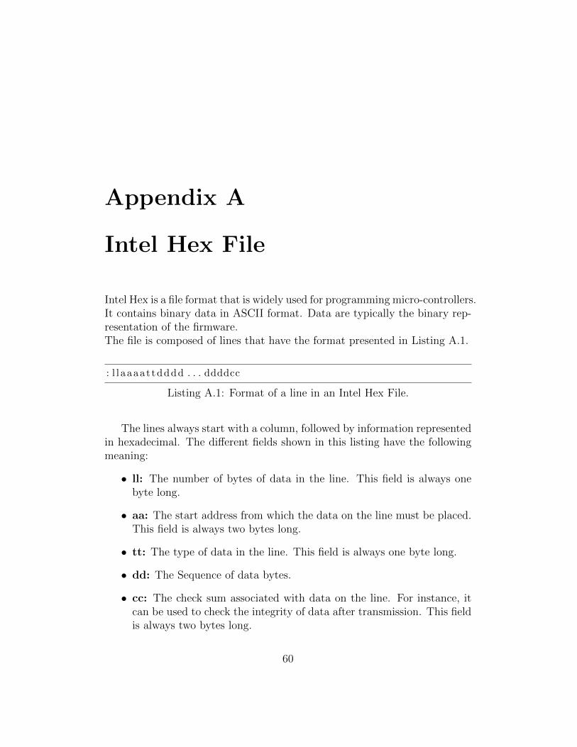
Appendix A
Intel Hex File
Intel Hex is a file format that is widely used for programming micro-controllers.It contains binary data in ASCII format. Data are typically the binary rep-resentation of the firmware.The file is composed of lines that have the format presented in Listing A.1.
: l l aaaat tdddd . . . ddddcc
Listing A.1: Format of a line in an Intel Hex File.
The lines always start with a column, followed by information representedin hexadecimal. The different fields shown in this listing have the followingmeaning:
• ll: The number of bytes of data in the line. This field is always onebyte long.
• aa: The start address from which the data on the line must be placed.This field is always two bytes long.
• tt: The type of data in the line. This field is always one byte long.
• dd: The Sequence of data bytes.
• cc: The check sum associated with data on the line. For instance, itcan be used to check the integrity of data after transmission. This fieldis always two bytes long.
60

In this work, the tt field can take only two values, either 0 or 1. Value 0means that the associated line contains binary data, and value 1 is used tosignal the end-of-file.However, only two of the fields are used: the length, and obviously the data.Indeed, using the two pieces of information is sufficient to extract the binarycode contained in the file.
61

Appendix B
Code Composer Studio -Enabling the Hex filegeneration
The procedure that must be used in Code Composer Studio IDE v7.1.0 toallow the Hex File generation is the following:
1. Make a right click on the project name in the left panel.
2. Click on properties.
3. In the opened window, on the left panel, click onMSP430 Hex Utility.
4. In the right panel, check the Enable MSP430 Hex Utility check box.
5. In the left panel, click on Output Format Options.
6. In the right panel, click on the Output format drop down menu andselect Output Intel hex format (--intel, -i).
7. In the opened window, on the left panel, click onMSP430 Hex Utility.
8. In summary of flags set field, check that the content is--memwidth=8 --romwidth=8 --intel.
9. The configuration presented in Fig. B.1 should be obtained.
62

Figure B.1: Overview of the panel for Intel Hex File configuration.
63

Appendix C
Code Composer Studio -Configuration for initialization
The procedure that must be used in Code Composer Studio IDE v7.1.0 toensure that the entire flash memory is not erased while programming theMSP430 micro-controller is the following one:
1. In the left panel, make a right click on the project.
2. Click on properties.
3. In the opened window, on the left panel, click onDebug.
4. In the right panel, click on MSP43x Options.
5. In the Erase Options panel, select the optionReplace memory locations, retain unwritten memory
locations.
6. The configuration presented in Fig. C.1 should be obtained.
64

Figure C.1: Erase option selection in Code Composer Studio
65

Appendix D
Linker command filesmodifications
The listing D.1 presents the MEMORY directive configuration that must be usedwhen preparing the sending of an updated firmware.The start address of the flash memory is set to 0x4A00, such that it corre-sponds to the configuration presented in section 4.1.1. The interrupt vectorsare located in the address range from 0xFFE0 to 0xFFFF, this thus permitsto be sure that the 32 last bytes of the firmware that are sent are the inter-rupt vectors.One can also notice that the reset vector is placed at address 0xFFFE, whileits content is not physically placed at that position in the micro-controller.Indeed, the reset vector of the firmware is placed at address 0x1080. How-ever, this choice was made to ensure that the two last transmitted bytes ofan updated firmware are always the address of the first instruction that mustbe executed when booting on the firmware.
MEMORY{
SFR : o r i g i n = 0x0000 , l ength = 0x0010PERIPHERALS 8BIT : o r i g i n = 0x0010 , l ength = 0x00F0PERIPHERALS 16BIT : o r i g i n = 0x0100 , l ength = 0x0100RAM : o r i g i n = 0x1100 , l ength = 0x2800INFOA : o r i g i n = 0x1080 , l ength = 0x0080INFOB : o r i g i n = 0x1000 , l ength = 0x0080FLASH : o r i g i n = 0x4A00 , l ength = 0xB4E0
66
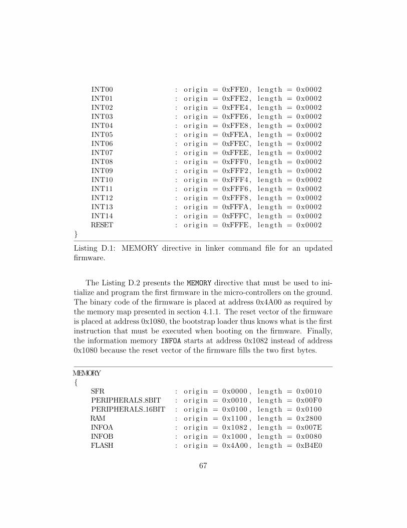
INT00 : o r i g i n = 0xFFE0 , l ength = 0x0002INT01 : o r i g i n = 0xFFE2 , l ength = 0x0002INT02 : o r i g i n = 0xFFE4 , l ength = 0x0002INT03 : o r i g i n = 0xFFE6 , l ength = 0x0002INT04 : o r i g i n = 0xFFE8 , l ength = 0x0002INT05 : o r i g i n = 0xFFEA, l ength = 0x0002INT06 : o r i g i n = 0xFFEC, l ength = 0x0002INT07 : o r i g i n = 0xFFEE, l ength = 0x0002INT08 : o r i g i n = 0xFFF0 , l ength = 0x0002INT09 : o r i g i n = 0xFFF2 , l ength = 0x0002INT10 : o r i g i n = 0xFFF4 , l ength = 0x0002INT11 : o r i g i n = 0xFFF6 , l ength = 0x0002INT12 : o r i g i n = 0xFFF8 , l ength = 0x0002INT13 : o r i g i n = 0xFFFA, l ength = 0x0002INT14 : o r i g i n = 0xFFFC, l ength = 0x0002RESET : o r i g i n = 0xFFFE, l ength = 0x0002
}
Listing D.1: MEMORY directive in linker command file for an updatedfirmware.
The Listing D.2 presents the MEMORY directive that must be used to ini-tialize and program the first firmware in the micro-controllers on the ground.The binary code of the firmware is placed at address 0x4A00 as required bythe memory map presented in section 4.1.1. The reset vector of the firmwareis placed at address 0x1080, the bootstrap loader thus knows what is the firstinstruction that must be executed when booting on the firmware. Finally,the information memory INFOA starts at address 0x1082 instead of address0x1080 because the reset vector of the firmware fills the two first bytes.
MEMORY{
SFR : o r i g i n = 0x0000 , l ength = 0x0010PERIPHERALS 8BIT : o r i g i n = 0x0010 , l ength = 0x00F0PERIPHERALS 16BIT : o r i g i n = 0x0100 , l ength = 0x0100RAM : o r i g i n = 0x1100 , l ength = 0x2800INFOA : o r i g i n = 0x1082 , l ength = 0x007EINFOB : o r i g i n = 0x1000 , l ength = 0x0080FLASH : o r i g i n = 0x4A00 , l ength = 0xB4E0
67

INT00 : o r i g i n = 0xFFE0 , l ength = 0x0002INT01 : o r i g i n = 0xFFE2 , l ength = 0x0002INT02 : o r i g i n = 0xFFE4 , l ength = 0x0002INT03 : o r i g i n = 0xFFE6 , l ength = 0x0002INT04 : o r i g i n = 0xFFE8 , l ength = 0x0002INT05 : o r i g i n = 0xFFEA, l ength = 0x0002INT06 : o r i g i n = 0xFFEC, l ength = 0x0002INT07 : o r i g i n = 0xFFEE, l ength = 0x0002INT08 : o r i g i n = 0xFFF0 , l ength = 0x0002INT09 : o r i g i n = 0xFFF2 , l ength = 0x0002INT10 : o r i g i n = 0xFFF4 , l ength = 0x0002INT11 : o r i g i n = 0xFFF6 , l ength = 0x0002INT12 : o r i g i n = 0xFFF8 , l ength = 0x0002INT13 : o r i g i n = 0xFFFA, l ength = 0x0002INT14 : o r i g i n = 0xFFFC, l ength = 0x0002RESET : o r i g i n = 0x1080 , l ength = 0x0002
}
Listing D.2: MEMORY directive in linker command file for initializingfirmware.
The Listing D.3 shows the MEMORY directive that is used for the linkercommand file used for the bootstrap loader.The flash memory section start at address 0x4000 but its length is reduced to0x0A00. Indeed, to respect the memory map presented in section 4.1.1, thebinary code of the bootstrap loader cannot be outside the addresses rangefrom 0x4000 to 0x4A00.Finally, it can be observed that the interrupt vectors of the bootstrap loaderis placed in the range from 0xFFE0 to 0xFFFF which is the same range asthe one used for the interrupt vectors of the firmware. The values placed atthese positions during the bootstrap loader programming, except the resetvector, are thus erased when the firmware is programmed. However, this isnot a problem as the bootstrap loader does not use any interruption.
MEMORY{
SFR : o r i g i n = 0x0000 , l ength = 0x0010PERIPHERALS 8BIT : o r i g i n = 0x0010 , l ength = 0x00F0PERIPHERALS 16BIT : o r i g i n = 0x0100 , l ength = 0x0100RAM : o r i g i n = 0x1100 , l ength = 0x2800
68

INFOA : o r i g i n = 0x1080 , l ength = 0x0080INFOB : o r i g i n = 0x1000 , l ength = 0x0080FLASH : o r i g i n = 0x4000 , l ength = 0x0A00INT00 : o r i g i n = 0xFFE0 , l ength = 0x0002INT01 : o r i g i n = 0xFFE2 , l ength = 0x0002INT02 : o r i g i n = 0xFFE4 , l ength = 0x0002INT03 : o r i g i n = 0xFFE6 , l ength = 0x0002INT04 : o r i g i n = 0xFFE8 , l ength = 0x0002INT05 : o r i g i n = 0xFFEA, l ength = 0x0002INT06 : o r i g i n = 0xFFEC, l ength = 0x0002INT07 : o r i g i n = 0xFFEE, l ength = 0x0002INT08 : o r i g i n = 0xFFF0 , l ength = 0x0002INT09 : o r i g i n = 0xFFF2 , l ength = 0x0002INT10 : o r i g i n = 0xFFF4 , l ength = 0x0002INT11 : o r i g i n = 0xFFF6 , l ength = 0x0002INT12 : o r i g i n = 0xFFF8 , l ength = 0x0002INT13 : o r i g i n = 0xFFFA, l ength = 0x0002INT14 : o r i g i n = 0xFFFC, l ength = 0x0002RESET : o r i g i n = 0xFFFE, l ength = 0x0002
}
Listing D.3: MEMORY directive in linker command file for the bootstraploader.
69
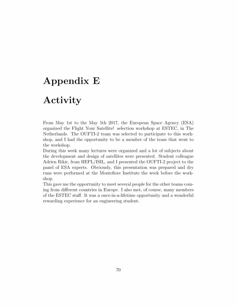
Appendix E
Activity
From May 1st to the May 5th 2017, the European Space Agency (ESA)organized the Flight Your Satellite! selection workshop at ESTEC, in TheNetherlands. The OUFTI-2 team was selected to participate to this work-shop, and I had the opportunity to be a member of the team that went tothe workshop.During this week many lectures were organized and a lot of subjects aboutthe development and design of satellites were presented. Student colleagueAdrien Rikir, from HEPL/ISIL, and I presented the OUFTI-2 project to thepanel of ESA experts. Obviously, this presentation was prepared and dryruns were performed at the Montefiore Institute the week before the work-shop.This gave me the opportunity to meet several people for the other teams com-ing from different countries in Europe. I also met, of course, many membersof the ESTEC staff. It was a once-in-a-lifetime opportunity and a wonderfulrewarding experience for an engineering student.
70

Figure E.1: Photo taken at the end of the OUFTI-2 project presentation atESTEC.
71

Bibliography
[1] Linker Command File Primer. http://processors.wiki.ti.com/
index.php/Linker_Command_File_Primer. Accessed: 2017-05-26.
[2] Ground systems and operations - Telemetry and telecommand packetutilization - ECSS-E-70-41A. Technical report, Jan. 2003.
[3] The Cubesat Program: Cubesat Design Specification - REV. 13. Tech-nical report, California Polytechnic State University, Feb 2014.
[4] N. Crosset. Implementation du relais D-STAR a bord du nanosatelliteOUFTI-1. Master’s thesis, Helmo Gramme, Liege, Belgium, 2010.
[5] Cypress Semiconductor Corporation. 2-Mbit (256K x 8) Serial (SPI)F-RAM, Aug. 2015.
[6] S. De Dijcker. Implementation de la gestion des telecommandes et destelemetries au sein de l’ordinateur de bord du nanosatellite OUFTI-1.Master’s thesis, Haute Ecole de la Province de Liege, Liege, Belgium,2011.
[7] S. De Dijcker. Fly your satellite 2017 - cubesat proposal OUFTI-2.Technical report, University de Liege, March 2017.
[8] A. Dunkels, N. Finne, J. Eriksson, and T. Voigt. Run-time dynamiclinking for reprogramming wireless sensor networks. In Proc. the 4thinternational conference on Embedded networked sensor systems, pages15–28, Nov 2006.
[9] C. Han, R. Kumar, R. Shea, E. Kholer, and M. Srivastava. A dy-namic operating system for sensor nodes. In Proc. the Third Conferenceon Mobile Systems, Application, and Services. MobiSys, pages 163–178,2005.
72

[10] J. W. Hui and D. Culler. The dynamic behavior of a data dissiminationprotocol for network programming at scale. In Proc. of the 2nd Interna-tional Conference on Embedded Network Sensor Systems. ACM, pages81–94, 2004.
[11] M. Iwinski and J. Sosnowski. Remote software reprogramming in em-bedded systems. PAK, 58(8):769–771, 2013.
[12] E. Lenchak. CRC Implementation With MSP-430. Texas Instruments,Nov. 2004.
[13] P. Levis and D. Culler. Mate: A Tiny Virtual Machine for SensorNetworks. ACM SIGARCH Computer Architecture News, Aug. 2002.
[14] R. Olivier, A. Wilde, and E. Zaluska. Reprogramming Embedded Sys-tems at Run-Time. In Proc. the 8th International Conference on SensingTechnology, Sep. 2014.
[15] A. Slavinskis and al. Firmware updating systems for nanosatellites.IEEE Aerospace and Electronic Systems for Nanosatellites, May 2016.
[16] Texas Instruments. MSP430x1xx Familly User’s Guide, 2006.
73