master - digital.library.unt.edu · was discovered in 1880 by sir william crooks. ... radiant...
TRANSCRIPT

Coatings and Alternatives for SEM Microscopy*
Richard H. Lee
Energy Technology Division Argonne National Laboratory
Argonne, IL 60439
March 1995
by .a contractor of the U.S. Government under contract No. W-31-104ENG-38. Accordingly, the U. S Government retains a nonexclusive, royalty-free license to publish or reproduce the published form of this contribution, or allow others to do so, for
d PI
. Presented at INTER/MICR0'93, July 19, 1993, Chicago, IL
*Work supported by the Tribology Program, Office of Transportation Materials, U.S. Department of Energy, under Contract W-3 1-1 09-Eng-38.
BlSTRlEUTION OF THIS DOCUMENT IS UNLIMITED !35 MASTER

DISCLAIMER
Portions of this document may be illegible in electronic image products. Images are produced from the best available original document

COATINGS AND ALTERNATIVES FOR SEM MICROSCOPY *
Richard H. Lee Argonne National Laboratory
Argonne, Illinois 60439-4838
Key Words: carbon, chromium, coating, gold, low voltage, platinum, scanning
electron microscope, sputtering, structure
ABSTRACT
Several methods of preparing samples of low electrical conductivity for
conventional scanning electron microscopy are reviewed. Two new methods
are chromium sputter-coating and low-voltage electron microscopy with a field
emission gun. Photomicrographs of different coatings at high magnification
show the structure of each coating. Advantages and disadvantages of each
material are presented. Results with sputtered coatings are compared to an
evaporated carbon coating.
HISTORY
Coating is commonly done today by magnetron glow discharge or plasma
sputter coating. Glow discharge (electrical conduction in a low-pressure gas )
was discovered in 1880 by Sir William Crooks. In 1892, Tesla demonstrated his
radiant illumination tubes of rarefied gases in Paris and again in Chicago at the
Columbian Exhibition . Tesla's attempts to build interest in high-voltage
*Presented at INTEWMICR0'93, July 19,1993, Chicago IL
1
experiments were not successful until much later. Some people even
feared that Tesla's experiments might ignite the atmosphere1.h 1928, Lang-
muir named the phenomenon plasma and identified it as a new state of matter.
INTRODUCTION
The process of sputter-coating samples for scanning electron microscopy has
been covered in other reference texts *,3. Materials with low electrical
conductivity or high resistivity are difficult to image because of charge build
up. This phenomenon disrupts both the generation of secondary electrons
for imaging and the excitation of characteristic X-rays for microanalysis4. The
first decision is the choice of coating material, and the second decision is the
choice of a process for coating (the conductive path to ground). High-
vacuum evaporation has been used since the late 1940's for electron
microscopy samples and is still a useful technique. Carbon is evaporated by
DC resistive heating and is still the material of choice for microanalysis, for
it has excellent transparency and is inert and electrically conductive.
Metal coatings such as aluminum have been tried, but any metal coating will
absorb significant amounts of soft X-ray signals. Sputter-coating is a physical
vapor deposition process that uses a plasma generated by ionizing a low-
pressure inert gas such as argon with a target of a noble metal . The
metals most commonly used are gold, silver, platinum, palladium, and now
2

chromium . Except for chromium, all have good sputtering yields and can be
sputtered in a low partial pressure atmosphere after evacuation with a
mechanical vacuum pump. The heavier metals such as gold also have high
secondary electron yields, making imaging much easier. Table 1 shows typical
parameters for various target materials in our commercial sputtering unit.
Table 1 - Sputtering Parameters
For average thickness of 15 nm in 7 Pa argon gas pressure
MATERIAL PLASMA (mA) TIME (sec)
gold (pure) 15 90
gold/Pd 15 120
silver 15 120
platinum 15 180
copper 25 120*
nickel 50 90*
c h romi um 100 300*
* requires pre-sputter with a target shutter and 10 Pa pressure
The main disadvantage of gold and silver coatings is their tendency to migrate
on the surface of the sample and coalesce into islands or particles. This prop-
erty is utilized to make resolution test samples for the scanning electron micro-
3
scope (SEM). For higher-resolution imaging, we need a coating with much
smaller particle size, e.g., platinum or chromium. Platinum's particle size is
smaller than gold, but not nearly as good as chromium. In our work, we must
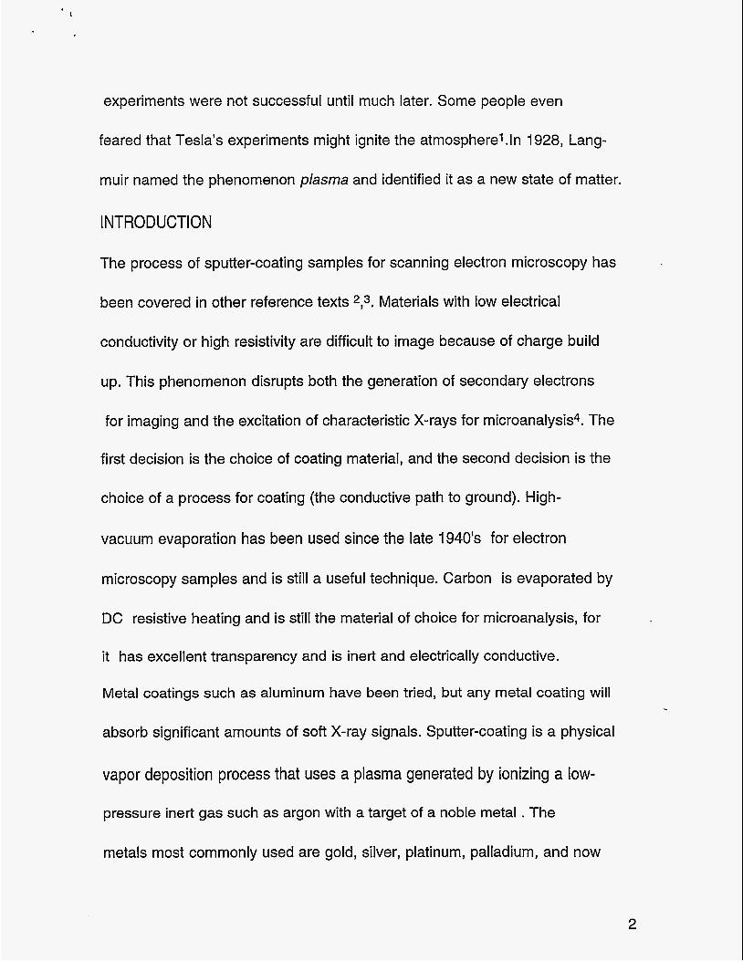
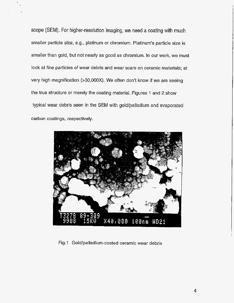
look at fine particles of wear debris and wear scars on ceramic materials; at
very high magnification (>30,00OX). We often don't know if we are seeing
the true structure or merely the coating material. Figures 1 and 2 show
typical wear debris seen in the SEM with gold/palladium and evaporated
carbon coatings, respectively.
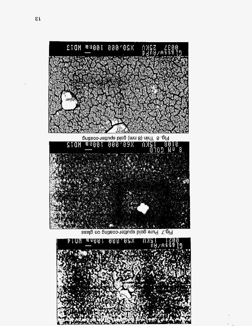
Fig. 1 Gold/palladium-coated ceramic wear debris
4
Fig.2 Carbon-coated ceramic wear debris (SEM)
To resolve this analytical problem, we decided to examine, with the SEM,
the structure of our available coating target materials and compare them. We
subsequently sputtered coatings of the typical thickness onto one side of
clean microscope glass slides. One slide was also coated with carbon by resis-
tive evaporation in the sputtering system accessory unit. Pieces were cut from
the glass slides and examined in the SEM, and photomicrographs were taken
at the same magnification; 50,OOOX. After this experiment, a sample of a glass
slide sputter-coated with chromium by a commercial manufacturer was obtained
and examined in the same manner. Finally, a new SEM with a field emission -
gun (FEG) was used to examine a diamond-film on a sample that we did not
wish to coat with any other material. Diamond films are difficult to image
because of their high resistivity and frequently have very fine structure or grain
5

size. The differences in resolution between the uncoated low-voltage (1 OkV)
mode with the conventional SEM and the low-voltage (5kV) FEG/SEM is shown
Y *" " ,
92-6-5a C E n t 3560 10KV X 2 0 # 0 0 0 1tJm 61015
1 L- SE1 EHT- 5.00 KV UD= 5 m IItlG- X 30.0 K PHOTO- 34 1.ooum I
-- Fig. 4 FEG/SEM image of fine-grained diamond film
6

MATERIALS AND EQUIPMENT
Pure metal foils were used for sputtering targets, and the carbon source was
spectrographic-grade graphite fiber, all obtained from the manufacturer of our
coating system (Bakers SCD-040 with capabilities for evaporation, etching
in plasma, and sputtering). Carbon is evaporated by attaching a special
glass chamber and flange with feedthroughs for DC heating (Fig. 5). To control
coating thickness, we used a quartz crystal thickness monitor (Balzers #QSG-
301).
Fig.5 Coating system with evaporation accessory
The vacuum system is a direct-drive mechanical pump capable of 1 Pa
pressure (0.01 mbar).We have targets of copper, silver, gold, gold/ palladium,
and platinum. The SEM used in the study is a JEOL 840A with a tungsten
(conventional) filament. The FEG /SEM used in the comparison study was a
7

Leica-Cambridge Stereoscan 360FE, courtesy of Leica Inc. of Deerfield, Illinois.
The coating system is available with several additional features that may be
desirable. A movable shutter to cover the target is useful to shield the sample
from contamination during startup or plasma etching (when the polarity is rev-
ersed and deposition could occur on the target). Sample rotation is useful,
especially when several samples are being coated simultaneously or during
evaporation. Evaporation is a straight-line process, while sputtering is a
random process; in which deposition is from many directions. A film thickness
monitor is useful in controlling coating thickness, especially when experiment-
ting with new conditions or materials. One need only program the atomic weight
of the target material and the desired thickness in nanometers. The monitor will
indicate the coating thickness and shut off the process when the desired
thickness has been reached. During carbon evaporation, the crystal monitor
may overheat because of flash heating, so one may have to allow the monitor
to cool before taking a reading. Plasma etching is a very desirable feature,
especially on materials that may have surface contamination or absorbed
moisture (such as salt crystals).
The best vacuum of the coating system is very important to the quality of the
coatings. In general, the better the vacuum, the better the coating. Pumping
speed is also a factor in coatings, and a turbomolecular pump is very desirable
8
because of their fast pump-down and minimal back streaming contamination.
The quality of the vacuum necessary depends on the material being used for
coating. Aluminum, chromium, and nickel require very low pressure and a very
clean atmosphere because of their affinity for oxidation. It may be necessary to
use an ultrahigh-purity gas or an auxiliary gas purification system for metals
such as chromium. Of course, this adds to the cost of coating, which becomes
another factor in selecting the coating material.
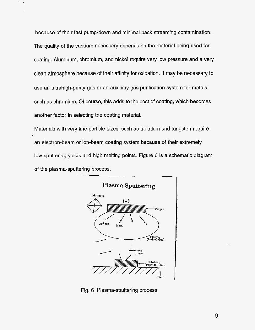
Materials with very fine particle sizes, such as tantalum and tungsten require
an electron-beam or ion-beam coating system because of their extremely .
low sputtering yields and high melting points. Figure 6 is a schematic diagram
of the plasma-sputtering process. - - -
Plasma Sputtering Magnets
Fig. 6 Plasma-sputtering process
9

A new coating technique for high-resolution imaging with the SEM has recently
been reported by Horrrigan and Window 5, in which a dual-target system is
used; titanium is used first to getter the atmosphere before coating is carried out
in xenon gas. There are other ways of removing unwanted contaminants from
the coating system atmosphere:
* Outgassing , usually by heating.
* Condensation , most commonly by liquid nitrogen.
* Trapping , usually for oil vapors.
* Flushing , or purging with inert gas.
Flushing is commonly employed in a sputter coater to help sweep air and
moisture from the chamber and also to permeate crevices and help remove
adsorbed gas.
The actual process of sputter deposition is a function of several factors.6,7 In
general, the speed or rate of deposition depends upon (a) gas type and press-
ure, (b) potential between target and workpiece, (c) current density, (d) distance
from target to workpiece, and (e) time ( thickness is linear with time).
Plasma etching is useful for samples that are difficult to clean, improving
bonding, and roughening a surface without the use of wet chemicals.
Plasma etching is done after evacuation by using a higher-pressure gas than
in sputtering and the sample is the target for the ions of the gas being used.
10

More plasma power and higher gas flow through the system are also generally
used. Plasma etching may also be accelerated by using a reactive gas mixture
instead of an inert gas. Removal of heavier carbon deposits may require a gas
mixture containing oxygen while ceramics etch much faster when a gas with
fluorine or chlorine is used to produce a volatile (gaseous) reaction products.
Carbon coating has three main features. First, it is virtually transparent be-
cause of its low density and low thickness. Second, it is amorphous and thus
usually has no structure. Third, it has low secondary-electron emission.
When evaporative carbon coating, there are two main kinds of pure graphite
materials; rods and fibers. Carbon rods require some preparation , usually
reducing the diameter at the tips. But, rods usually last much longer since they
can be reused. There are also composite rods available, with an addition of a
metal such as platinum for better resolution and reflectivity.
Normal conditions for sputter-coating were: (a) argon pressure 5-8Pa, (b)
plasma current 15 mA, (c) target-to-sample distance 30-40 mm; the result is a
thickness of 15 nm. Carbon evaporation was done with two graphite threads in
the best obtainable vacuum for 30 sec.
RESULTS
Examining the photomicrographs in Figs.7-12, one can compare the structure
11

and particle size of the coating materials. The irregular white objects
in the photos are dust particles that were probably on the surface of the glass
slides before coating. The polished glass microscope slides are extremely
smooth, making them difficult to image. The dust particles aid in critical
focusing of the surface and were the only objects that could be seen on the car-
bon-coated glass sample in the SEM (Fig.10).
These coatings were made under the same “normal” conditions, except for Fig.
8, which shows the structure of pure Au sputtered for a shorter time (8 nm thick).
The particle size is about the same as that in the 15 nm coating in Fig.7, but has
not yet broken up into islands. Our experience indicates that finer-grained
coatings can be obtained by lower plasma currents and the thinnest possible
coatings. Figure 11 shows a platinum coating; the dark area at the right is
from focusing at a higher magnification. The darkening is due to rapid carbon
buildup on the platinum, which is a good catalyst; this could be a problem
when the electron beam scans over a fixed area for several minutes or more.
Silver exhibits this same effect also.
Coatings that are only a few nanometers in thickness may also be optically
transparent.
12
E l
- I
Figure 12 is a photomicrograph of sputtered chromium from a typical "bench-
top" turbo-pumped coating system. The white object near the center is prob-
ably a dust particle on the glass slide. No particles could be resolved in the
chromium coating with the SEM. Figure 12b is a Y-Z modulation secondary- -
electron image of the same area shown in Fig. 12. The topography is enhanced
(amplified), but still no coating structure could be resolved.
14

Fig. 12 Chromium sputter-coating on glass
Fig. 12b Chromium sputter-coating ( Y-Z modulation)
Figure 3 shows an uncoated diamond film on silicon taken with the JEOL
SEM. The particle size is barely discernible. But when compared to the
photomicrograph of the same sample taken with the FEG/SEM (Fig. 4), the
coating structure is clearly resolved. Beam voltage in the FEG/SEM was 5 kV.
15

We did not want to coat the diamond films because we sometimes wish to
examine the structure with laser-Raman spectroscopy. However, if one does not
have access to an FEG/SEM, such a sample could be sputter-coated, examined
in the SEM, and then plasma etched to remove the sputtered coating. We have
coated hard carbon coatings with gold after microhardness testing in order to
make the tiny impressions visible in the microscope for measurement.
i I I
r 3
I I I I
c C I R C A C T
f. iF1 AG Ji-~...nA,TL .. ... i ; .. i i . . . A I _ _ , _ 11 E . . . . L
~ .- -. ..
Fig. 13 X-ray spectrum of thin Cr coating on glass
The spectrum in figure 13 is an energy-dispersive X-ray analysis of the area in
Fig. 12, showing that the chromium coating is so thin that significant
X-ray peaks for silicon and calcium (the two main elements in the glass sub-
strate) are clearly evident. We prefer to use sputtered metal coatings on our
ceramic wear samples because we obtain better coverage, fewer charging
problems, and much better electron reflectivity. Fortunately, the structure of the
16

wear debris in Fig. 1 was indicative of the actual particle size, mainly because of
the very thin metal coating. Particle size of the wear debris was smaller than we
expected.
The three main alternatives to coating for low-conductivity samples in the SEM
are (a) using lower electron beam voltage (< 5 kV ), (b) using a partial-
pressure environment (low-vacuum SEM, also called an “environmental SEM”),
and (c) using a nitrogen “flood gun” attachment that flushes a small sample area
under the beam with a gas that ionizes, thus dissipating the charge. Recently, a
new method of glycol infusion has been published for preparation of biological
specimens for the SEM9.
CONCLUSIONS
Gold coating is still useful for routine imaging when X-ray microanalysis is not
needed. Platinum coating has better resolution for conventional SEM imaging,
but chromium is the current material of choice for high-resolution imaging and
possibly X-ray spectroscopy because it can be used as thin as a few nano-
meters, Carbon coating remains useful, mainly for microanalysis. Low-voltage
imaging, especially with a FEG/SEM, is an excellent alternative to coating and
provides the best resolution. The only limitation to low-voltage electron micros-
copy is failure to excite high energy X-ray peaks for microanalysis.
17

REFERENCES
1. Cheney, M.; Tesla: Man out of Time, Dorset Press, New York 1981.
2. Goldstein, J. I. et ai; Scanning Electron Microscopy and X-ray Microanalysis, Plenum Press, New York 1981.
3. Postek, M.T. et al; Scanning Electron Microscopy: A Student's Handbook, Ladd Research, 1980.
4. Miller, D., "Artifacts of specimen charging in X-ray microanalysis in the Scan- ning electron microscope", Ultramicroscopy 1990 35, 357-366.
5. Horrigan, E.C. and Window, B., "A New Coating Technique for High Resolu- tion SEM Samples", Journal of Computer-Assisted Microscopy, 1 992 Vo1.4 NO. 2, 167-1 70.
6. Hill, R.J.; Physical Vapor Deposition, Temescal, Berkeley CA, 1986.
7. Wasa, K. and Hayakawa, S.; Handbook of Sputter Deposition Technology, Noyes, Park Ridge NJ 1992.
8. Ajayi, O.O., Lee, R.H., and Cook, R.E., "Plasma Etching of Structural Ceramics for Microstructural Analysis", Materials Science and Engineering 1993 A I 69 L5.
9. Ensikat, H.J. and Barthlott, W., "Liquid Substitution: a Versatile Procedure for SEM Specimen Preparation of Biological Materials without Drying or Coat- ing", Journal of Microscopy 1993 Vol. i 72 Pt. 3, 195-203.
18