master’s student initiation to scanning probes and ... · master’s student initiation to...
TRANSCRIPT
Master’s Student Initiation to Scanning Probes and Electronic Microscopes via Research Projects in Nanosciences
M.L. Della Rocca1,2, V. Repain1,2, Y. Gallais1,2, L. Doyennette1,3, F. Raineri1,4 and A. Anthore1,4 1 Université Paris Diderot, Sorbonne Paris Cité, Département de physique, 4 rue Elsa Morante, 75013 PARIS, France 2 Université Paris Diderot-CNRS, Laboratoire Matériaux et Phénomènes Quantiques, UMR 7162, 75013 PARIS, France 3 Université Montpellier 2-CNRS, Laboratoire Charles Coulomb, UMR 5221, F-34095 MONTPELLIER, France 4 CNRS, Laboratoire de Photonique et Nanostructures, UPR 20, 91460 MARCOUSSIS, France
The Physics Department of Paris Diderot University has built a nanosciences platform, which includes educational microscopes (AFMs, STMs, SEM and TEM) dedicated to teaching programs. To illustrate the skills developed by students in microscopy, we present here some research projects in nanosciences focused on carbon devices using graphene and nanotubes. Scanning probe microscopy, Raman spectroscopy and electronic microscopy are used to characterize structurally these materials, and to determine their position on a substrate, in order to enable the realization of electrical contacts. The materials are then further characterized by the field-effect modifications of their transport properties or optical properties. As a whole, such an experience represents a real immersion of the undergraduate students in the research world, giving them the unique opportunity to be initiated to different microscopy techniques.
Keywords: educational program; SEM/TEM; Scanning Probe Microscopy; Raman spectroscopy
1. Introduction to Research Projects in nanosciences on carbon devices
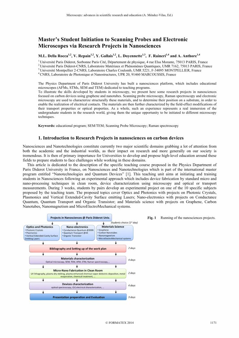
Nanosciences and Nanotechnologies constitute currently two major scientific domains grabbing a lot of attention from both the academic and the industrial worlds, as their impact on research and more generally on our society is tremendous. It is then of primary importance for Universities to develop and propose high-level education around these fields to prepare students to face challenges while working in these domains. This article is dedicated to the description of the specific teaching course proposed in the Physics Department of Paris Diderot University in France, on Nanosciences and Nanotechnologies which is part of the international master program entitled “Nanotechnologies and Quantum Devices” [1]. This teaching unit aims at initiating and training students in Nanosciences following an experimental approach which includes device fabrication by standard micro and nano-processing techniques in clean room, device characterization using microscopy and optical or transport measurements. During 3 weeks, students by pairs develop an experimental project on one of the 10 specific subjects proposed by the teaching team. The proposed topics cover Optics and Photonics with projects on Photonic Crystals, Plasmonics and Vertical Extended-Cavity Surface emitting Lasers; Nano-electronics with projects on Conductance Quantum, Quantum Transport and Organic Transistor; and Materials science with projects on Graphene, Carbon Nanotubes, Nanomagnetism and MicroElectroMechanical systems.
Fig. 1 Running of the nanosciences projects.
Microscopy: advances in scientific research and education (A. Méndez-Vilas, Ed.)__________________________________________________________________
1171© FORMATEX 2014
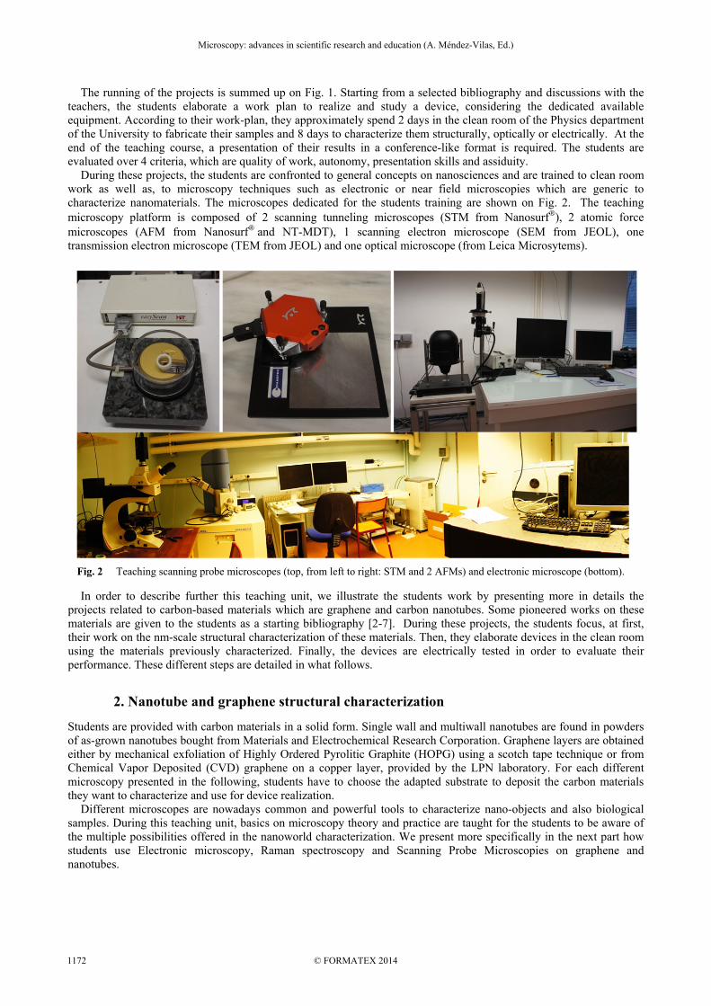
The running of the projects is summed up on Fig. 1. Starting from a selected bibliography and discussions with the teachers, the students elaborate a work plan to realize and study a device, considering the dedicated available equipment. According to their work-plan, they approximately spend 2 days in the clean room of the Physics department of the University to fabricate their samples and 8 days to characterize them structurally, optically or electrically. At the end of the teaching course, a presentation of their results in a conference-like format is required. The students are evaluated over 4 criteria, which are quality of work, autonomy, presentation skills and assiduity. During these projects, the students are confronted to general concepts on nanosciences and are trained to clean room work as well as, to microscopy techniques such as electronic or near field microscopies which are generic to characterize nanomaterials. The microscopes dedicated for the students training are shown on Fig. 2. The teaching microscopy platform is composed of 2 scanning tunneling microscopes (STM from Nanosurf®), 2 atomic force microscopes (AFM from Nanosurf® and NT-MDT), 1 scanning electron microscope (SEM from JEOL), one transmission electron microscope (TEM from JEOL) and one optical microscope (from Leica Microsytems).
In order to describe further this teaching unit, we illustrate the students work by presenting more in details the projects related to carbon-based materials which are graphene and carbon nanotubes. Some pioneered works on these materials are given to the students as a starting bibliography [2-7]. During these projects, the students focus, at first, their work on the nm-scale structural characterization of these materials. Then, they elaborate devices in the clean room using the materials previously characterized. Finally, the devices are electrically tested in order to evaluate their performance. These different steps are detailed in what follows.
2. Nanotube and graphene structural characterization
Students are provided with carbon materials in a solid form. Single wall and multiwall nanotubes are found in powders of as-grown nanotubes bought from Materials and Electrochemical Research Corporation. Graphene layers are obtained either by mechanical exfoliation of Highly Ordered Pyrolitic Graphite (HOPG) using a scotch tape technique or from Chemical Vapor Deposited (CVD) graphene on a copper layer, provided by the LPN laboratory. For each different microscopy presented in the following, students have to choose the adapted substrate to deposit the carbon materials they want to characterize and use for device realization. Different microscopes are nowadays common and powerful tools to characterize nano-objects and also biological samples. During this teaching unit, basics on microscopy theory and practice are taught for the students to be aware of the multiple possibilities offered in the nanoworld characterization. We present more specifically in the next part how students use Electronic microscopy, Raman spectroscopy and Scanning Probe Microscopies on graphene and nanotubes.
Fig. 2 Teaching scanning probe microscopes (top, from left to right: STM and 2 AFMs) and electronic microscope (bottom).
Microscopy: advances in scientific research and education (A. Méndez-Vilas, Ed.)__________________________________________________________________
© FORMATEX 20141172

2.1 Electronic microscopies
Scanning and transmission electron microscopies (SEM-TEM) are used to characterize multi- and single-wall carbon nanotubes (SWNTs, MWNTs) before device fabrication. This investigation has the double scope to extract the main characteristics of the nanotubes, such as dimensions and purity, and to identify the nanotube to electrically connect to realize nanotube-based field effect transistor. The resolution of the SEM being of ~10-20 nm, only MWNTs can be clearly visualized with such a microscope, TEM is therefore more suitable to explore SWNTs. Solutions with variable concentration (from ~50 µg/cm3 to ~ 1.5 mg/cm3) are obtained by dispersing powders of MWNTs and SWNTs in ethanol. After one hour US sonication to avoid the formation of aggregates, nanotubes are dispersed on a silicon substrate for SEM analysis or on standard Cu meshed grid covered by a thin holed carbon layer for TEM. MWNTs are spin coated (30 sec at 5000 rpm) on a Si/SiO2 (300 nm) substrate and installed in the vacuum chamber of the microscope. Figure 3 shows two typical SEM images using an acceleration voltage of 15 kV and the secondary electron (SE) detector for the minimal (a) and maximal (b) concentrations of MWNT.
Fig. 3 SEM images of MWNTs spin coated on a Si/SiO2 substrate, two different concentrations of MWNT solutions are used, ~50 µg/cm3 (a) and ~1.5 mg/cm3 (b). In spite of the sonication, aggregates of MWNTs are always visible on large area images and are more frequent in the high concentrated case (Fig. 3 b). For the lower concentration (Fig. 3 a), at higher magnification isolated nanotubes are clearly distinguishable, the estimated number of MWNTs per unit area is 0.01 µm-2, which is a good density to easily realize metallic contact on an isolated tube without being affected by other tubes short circuiting the device. A closer inspection (Fig. 4 a) allows the determination of the MWNTs dimensions: typical diameters of ~150 nm are founded in agreement with the product datasheet (140 nm), the length is instead very variable, from few µm to 10-20 µm.
Figure 4 a) also clearly shows that MWNTs exhibit a number of twists and that Y-shaped nanotubes are present. SEM is also equipped with a detector for Energy Dispersive X-ray Spectroscopy (EDS), this analysis is performed to have more insight on the purity of the nanotubes. Figure 4 b) shows an EDS spectra for an aggregate of MWNTs dispersed on a gold layer: C, Si and Au spectral lines are evident, spectral lines corresponding to Fe, the catalyst
Fig. 4 a) SEM images of few MWNTs, the minimal measurable diameter is ~150 nm, length varies from few µm to 10-20 µm. b) EDS spectra performed on an aggregate of MWNTs.
1 µm a)
10 µm 10 µm
10 µm
a) b)
E(kV)
b)
Fe Fe
Au
C
Si
Microscopy: advances in scientific research and education (A. Méndez-Vilas, Ed.)__________________________________________________________________
1173© FORMATEX 2014
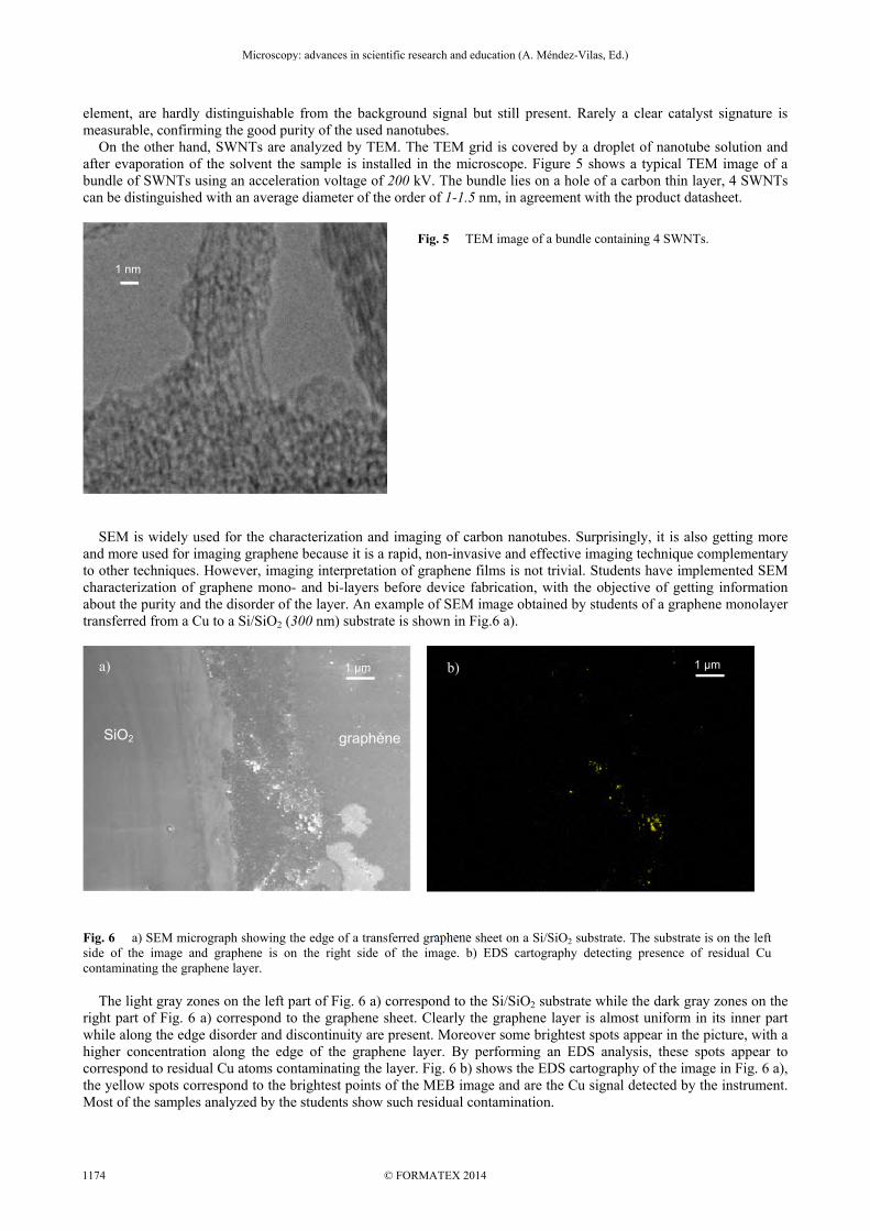
element, are hardly distinguishable from the background signal but still present. Rarely a clear catalyst signature is measurable, confirming the good purity of the used nanotubes. On the other hand, SWNTs are analyzed by TEM. The TEM grid is covered by a droplet of nanotube solution and after evaporation of the solvent the sample is installed in the microscope. Figure 5 shows a typical TEM image of a bundle of SWNTs using an acceleration voltage of 200 kV. The bundle lies on a hole of a carbon thin layer, 4 SWNTs can be distinguished with an average diameter of the order of 1-1.5 nm, in agreement with the product datasheet.
Fig. 5 TEM image of a bundle containing 4 SWNTs.
SEM is widely used for the characterization and imaging of carbon nanotubes. Surprisingly, it is also getting more and more used for imaging graphene because it is a rapid, non-invasive and effective imaging technique complementary to other techniques. However, imaging interpretation of graphene films is not trivial. Students have implemented SEM characterization of graphene mono- and bi-layers before device fabrication, with the objective of getting information about the purity and the disorder of the layer. An example of SEM image obtained by students of a graphene monolayer transferred from a Cu to a Si/SiO2 (300 nm) substrate is shown in Fig.6 a).
Fig. 6 a) SEM micrograph showing the edge of a transferred graphene sheet on a Si/SiO2 substrate. The substrate is on the left side of the image and graphene is on the right side of the image. b) EDS cartography detecting presence of residual Cu contaminating the graphene layer. The light gray zones on the left part of Fig. 6 a) correspond to the Si/SiO2 substrate while the dark gray zones on the right part of Fig. 6 a) correspond to the graphene sheet. Clearly the graphene layer is almost uniform in its inner part while along the edge disorder and discontinuity are present. Moreover some brightest spots appear in the picture, with a higher concentration along the edge of the graphene layer. By performing an EDS analysis, these spots appear to correspond to residual Cu atoms contaminating the layer. Fig. 6 b) shows the EDS cartography of the image in Fig. 6 a), the yellow spots correspond to the brightest points of the MEB image and are the Cu signal detected by the instrument. Most of the samples analyzed by the students show such residual contamination.
a) b)
b)
b)
1 nm
1 µm 1 µm
SiO2 graphène
Microscopy: advances in scientific research and education (A. Méndez-Vilas, Ed.)__________________________________________________________________
© FORMATEX 20141174

2.2 Raman Spectroscopy
Raman spectroscopy is used to check whether students succeed to transfer only one graphene layer on a substrate. Thin graphene layers are deposited on Si/SiO2 substrates and first identified using optical microscopy by looking at their white light contrast in reflection geometry. The identification of the number of layers of pre-identified thin samples is made via Raman spectroscopy by mapping the lineshape of the 2D band which is a well-known marker of the number of layers. The 2D band of graphene layers arises from a second order Raman process where two transverse in-plane optical phonons with opposite momenta close to the Brillouin zone corner are created. Because the process is resonant with intermediate electronic states, the precise value of the phonon momenta and its energy is strongly dependent on the underlying electronic structure for a given laser energy. The difference in the 2D band lineshape thus purely arises from the band structure which is dependent on the number of graphene layers. For single layer graphene only a single electronic intermediate state is resonant, and consequently only a single Lorentzian phonon band is observed. With increasing number of layers, several electronic intermediate states become resonant, leading to an increasingly complex 2D band lineshape with a multiple peak structure. The Raman set-up used by the students is a home-built research confocal Raman microscope. The incoming laser beam (λ=532 nm) is focused on the graphene samples by a ×50 long working distance objective (N.A.= 0.5) and the spot dimension is about 1 μm. The Raman signal is collected via the same objective and focused on the entrance slit of a grating spectrometer equipped with a Nitrogen cooled CCD detector. Students mount their samples deposited on SiO2 wafers on a copper sample holder which is then attached mechanically to a xyz stage allowing them to perform Raman mapping with micron resolution. While the incoming optical path is already pre-aligned, students have to carefully align the collection optics with respect to the spectrometer entrance slit and mirrors in order to observe the Raman signal from their graphene samples. Typical spectra of the 2D band at around 2700 cm-1 obtained by the students for various spot positions on a thin sample are shown in Fig. 7. The evolution of the lineshape of the 2D band shows that the optical contrast between different regions, evident in the corresponding optical microscopy image of Fig. 7, arises from variation in layer thickness. In particular the presence of single layer graphene regions can be unambiguously determined by the presence of a single and almost symmetric Lorentzian-like 2D band (region b). By contrast regions with higher number of layers show multicomponent lineshapes consisting of several peaks which are significantly blue-shifted.
Fig. 7 a) Optical image of an exfoliated graphene sheet on a SiO2 substrate. b) Raman spectra at the different positions marked on the left image. Single graphene layers are located in b and c where the 2D band is a single Lorentzian located at a Raman Shift smaller than 2700 cm-1.
2.3 Scanning probe microscopies
Scanning probe microscopies are used to complement the structural characterization of graphene and nanotubes. Students first learn to use the Scanning Tunneling Microscope and the Atomic Force Microscope with “ideal” samples (surface of graphite and calibration grid for examples). An introduction to the different AFM modes available (tapping or contact) is given. Then they prepare their own sample with graphene or carbon nanotubes taking into account the specificities of each microscope (scanning windows, type of substrates …)
a) b)
Microscopy: advances in scientific research and education (A. Méndez-Vilas, Ed.)__________________________________________________________________
1175© FORMATEX 2014

Fig. 8 a) Scanning Tunneling Microscope image of graphene grown by chemical vapour deposition on copper. b) Atomic Force Microscope image of single wall carbon nanotube. c) Height profile on the red line of b) The 2 to 3 nm height structure is the nanotube. To perform scanning tunnelling microscopy, the CVD graphene is the most appropriated being directly on a conducting copper substrate. Using a 1.5×1.5 nm2 squared scanning area, a tunnel current of 1 nA and a voltage of 0.5 V, students succeed to obtain atomic resolution as shown on Figure 8 a). The observed structure is honeycombed as expected for graphene, with a measured lattice parameter of 0.26 ± 0.02 nm. The tabulated one is equal to 0.2456 nm. The corrugation is of the order of 20 pm at the resolution limit of the used STM. The observation of carbon nanotubes with the STM is more difficult. Even on a substrate of graphite with an atomically flat structure on hundred nanometers scales, no tubes were detected in the 600×600 nm2 scanning window. Most probably nanotubes are moved away when scanning with the STM tip .Students rapidly give up this observation to use more suitable tools. The Atomic Force Microscope (AFM) is more suited to observe carbon nanotubes. First, the substrate can be an insulator or a semiconductor: it is then possible to use crystalline wafer. The used substrate of silicon has a roughness smaller than 0.1 nm on two inches surface. Second, the scanning window is of 100×100 µm2. Multiwall nanotubes are easily found but the tip can push and break them even in the tapping mode. Single wall nanotubes seem to be more linked to the substrate by Van der Waals interactions. Figure 8 b) shows the image of an isolated carbon nanotube longer than 4 µm. On Fig. 8 c), the height profile is shown indicating that the tube has a diameter of 2.5 ± 0.5 nm. The apparent width of 2 µm is due to the tip convolution. The average diameter is consistent with the product datasheet. The limited speed of Scanning Probe microscopies prevents the students to use it as a localization tool. Yet, these characterizations allow them to check the structural characteristics of the materials they use to make a device.
3. Device realization and characterization
Once structural characterization achieved, students elaborate their own devices based on carbon nanotubes and graphene, this gives them the opportunity to discover cleanroom facilities and technological processes. Based on bibliographic research and discussions with the teaching team, students generally choose to realize a field-effect transistor where the active channel is made of graphene or nanotubes. This kind of devices at the root of microelectronics, allows students to get more insights in the main physical properties of these materials by looking at their properties under electrical stimulations. Besides field-effect like transistor based on graphene or nanotubes is quite easy to realize and characterize.
Microscopy: advances in scientific research and education (A. Méndez-Vilas, Ed.)__________________________________________________________________
© FORMATEX 20141176

3.1 Clean room processes
Fig. 9 Paris Diderot’s clean room. a) Lithography area with MJB4 mask aligner. b) Deposition-etching area.
The fabrication process of graphene and SWNTs-MWNTs based transistors is performed in the cleanroom platform (class 100 or ISO 5) of Paris Diderot University where optical lithography and evaporation facilities are installed. Figure 9 presents a picture of the lithography area (a) together with the deposition-etching area (b) of this cleanroom. The two types of devices are realized following an analogous approach. The main steps of the cleanroom fabrication process are summed up in the scheme of Fig. 10.
Fig. 10 Scheme illustrating the nanofabrication process of nanotubes and graphene based field effect transistor
Students start from a 2 inches wafer of highly p-doped Si (used as a backgate electrode) capped with 300 or 500 nm of SiO2. The 300 nm SiO2 is preferred for graphene-based device in order to improve the visibility of the graphene layer by optical microscopy. The SiO2 layer is the insulating layer allowing a capacitive coupling of the Si substrate to the device for electrical characterization and is also used to realize a map marker. Such map marker is necessary for the localization of the carbon nanotube or the graphene layer that will be chosen to realize the transistor. The map marker is realized by optical lithography through a positive resist (S1805) followed by reactive ion etching (RIE), the etching depth of the SiO2 layer is of the order of 50 nm. The resist is then removed with acetone and oxygen plasma. An image of the obtained map marker is shown in Fig. 10, each square contain a binary code individuating the row and column position.
a)
b)
40µm
Microscopy: advances in scientific research and education (A. Méndez-Vilas, Ed.)__________________________________________________________________
1177© FORMATEX 2014
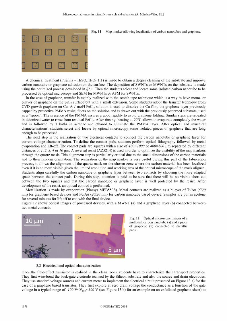
Fig. 11 Map marker allowing localization of carbon nanotubes and graphene.
A chemical treatment (Pirahna – H2SO4:H2O2 1:1) is made to obtain a deeper cleaning of the substrate and improve carbon nanotube or graphene adhesion on the surface. The deposition of SWNTs or MWNTs on the substrate is made using the optimized process developed in §2.1. Then the students select and locate some isolated carbon nanotube to be processed by optical microscopy and SEM for MWNTs or AFM for SWNTs. In the case of graphene, transfer is mainly realized with the scotch tape technique which is a way to have mono- or bilayer of graphene on the SiO2 surface but with a small extension. Some students adopt the transfer technique from CVD growth graphene on Cu. A 1 mol/l FeCl3 solution is used to dissolve the Cu film, the graphene layer previously capped by protective PMMA resist, floats on the solution and is drawn out with the previously patterned substrate, used as a “spoon”. The presence of the PMMA assures a good rigidity to avoid graphene folding. Similar steps are repeated in deionized water to rinse from residual FeCl3. After rinsing, heating at 90°C allows to evaporate completely the water and is followed by 3 baths in acetone and ethanol to eliminate the PMMA layer. After optical and structural characterizations, students select and locate by optical microscopy some isolated pieces of graphene that are long enough to be processed. The next step is the realization of two electrical contacts to connect the carbon nanotube or graphene layer for current-voltage characterization. To define the contact pads, students perform optical lithography followed by metal evaporation and lift-off. The contact pads are squares with a size of 400×1000 or 400×800 µm separated by different distances of 1, 2, 3, 4 or 10 µm. A reversal resist (AZ5214) is used in order to optimize the visibility of the map markers through the quartz mask. This alignment step is particularly critical due to the small dimensions of the carbon materials and to their random orientation. The realization of the map marker is very useful during this part of the fabrication process, it allows the alignment of the quartz mask on the chosen zone where the carbon material has been localized even if it is no more visible given the limited resolution and working area of the optical microscope of the mask aligner. Students align carefully the carbon nanotube or graphene layer between two contacts by choosing the more adapted space between the contact pads. During this step, attention is paid to be sure that there will be no visible short cut between the two squares and that the carbon nanotube or graphene layer is well protected by the resist. After development of the resist, an optical control is performed. Metallization is made by evaporation (Plassys MEB550S). Metal contacts are realized as a bilayer of Ti/Au (5/20 nm) for graphene based devices and Pd/Au (20/20 nm) for carbon nanotube based device. Samples are put in acetone for several minutes for lift off to end with the final device. Figure 12 shows optical images of processed devices, with a MWNT (a) and a graphene layer (b) connected between two metal contacts.
Fig. 12 Optical microscope images of a multiwall carbon nanotube (a) and a piece of graphene (b) connected to metallic pads.
3.2 Electrical and optical characterization
Once the field-effect transistor is realised in the clean room, students have to characterize their transport properties. They first wire-bond the back-gate electrode realised by the Silicon substrate and also the source and drain electrodes. They use standard voltage sources and current meter to implement the electrical circuit presented on Figure 13 a) for the case of a graphene based transistor. They first explore at zero drain voltage the conductance as a function of the gate voltage in a typical range of -100 V<Vgate<100 V (see Figure 13 b) for an example on an exfoliated graphene sheet) to
a) b)
Microscopy: advances in scientific research and education (A. Méndez-Vilas, Ed.)__________________________________________________________________
© FORMATEX 20141178

have insight about field effect on their device. Afterwards they measure the full current-voltage characteristics. The experimental accuracy (which is limited by the used ohmmeter) and the limited range (10 %) on which the graphene sheet conductance changes do not allow the students to confirm they were measuring a monolayer of graphene. Yet, the order of magnitude of the measured conductance is comparable to the one obtained in [8].
Fig. 13 a) Schematics of the field effect transistor realised with a graphene sheet. The silicon substrate plays the role of the gate biased at VG, a thermal oxide of 500 nm insulates the gate from the transistor channel. Drain source current ID as a function of the drain bias voltage VD can be measured. b) Differential conductance dID/dVD at VD=0 of a graphene layer as a function of VG.
As another example, Figure 14 represents the current-voltage characteristics as a function of the gate voltage for a multiwall carbon nanotube based transistor for gate voltages equal to 0, 20, 40, and 80 V. In that case despite the typical metallic nature of MWNTs, the field effect might be due to the fact that the coupling from the electrodes to the tube is only to the outer shell, this outer shell being semiconducting. Another possible explanation can be evoked: the presence of twists in the nanotube structure once deposited on the substrate (as shown in § 2.1) can open a gap, inducing a semiconducting behavior. As a consequence a small gate effect is detectable. Unfortunately, students burnt out their devices before changing the polarity of their gate voltage bias. They couldn’t infer parameters like carriers’ mobility, threshold voltage and on-off ratio.
Fig. 14 Current ID -voltage VD characteristic of a multiwall carbon nanotube at VG=0, 20, 40 and 80 V from bottom to up on the right.
Identified single graphene layer regions have been also connected to metallic electrodes defined by optical lithography (Fig. 12). This allows the students to follow the evolution of the Raman active G band phonon lineshape with an applied back gate voltage (Vg) between the doped Si layer and the metallic contact. The entire device is wired by the students and connected to a voltage source. It is then mounted on the xyz stage of the Raman set-up as the one used for the identification of the number of layers (§ 2.2). Because of electron-phonon coupling, optical phonons can decay into electron-hole pairs, a process known as Landau damping, making the energy and width (inverse lifetime) of phonons sensitive to the position of the chemical potential. In the case of graphene on SiO2, the chemical potential can be easily tuned by several hundreds of meV by an applied gate voltage. Depending on the position of the chemical potential the damping process can be allowed or blocked by Pauli exclusion principle. The effect is illustrated in Fig. 15 where the position of the G band is reported as a function of gate voltage. The G band energy shifts by several cm-1 illustrating a modulation of the electron-phonon coupling by the gate voltage. The observed non-monotonic behavior is due electron-hole symmetry with respect to the Dirac point of graphene and the gate voltage dependence of the G band energy can be used to determine the gate voltage where the chemical potential is located at the Dirac point.
Microscopy: advances in scientific research and education (A. Méndez-Vilas, Ed.)__________________________________________________________________
1179© FORMATEX 2014

4. Conclusion
In three weeks, the students build a project, read some bibliography, make, characterize and measure samples as small as graphene or carbon nanotube based transistor and finally analyse and present their results. The amount of impressive results obtained on these nano-devices by Master students in a very limited time shows them that the experimental study of nano-objects if far from being a sole research lab topic nowadays. Beyond the training on cleanroom and microscopy techniques, the students learn to think by themselves to solve the technical or more fundamental problems they face during this course. They can therefore feel that nanosciences is not only a textbook field but can be practically handled, with its tricks, clever idea and disappointment. This course takes place at the beginning of the year and certainly helps to motivate the students and to make more practical the theoretical lectures on quantum transport and others. Finally, by a reasonable investment over few years and with passionate teachers, the Physics Department of Paris Diderot University is now able to train its students on the basics of nanotechnologies. It is worth to note that this nanosciences platform is used far more widely than for the course developed in this article. It is now used for material sciences license students and for first year master students when teaching condensed matter physics and introduction to nanosciences. Other institutions like Ecole Normale Supérieure and Paris 13 University also benefit from those instruments for their students. The feedback from the students shows that this pedagogical tool is a success and we hope that its presentation can influence other institutions to create such practical platforms for the teaching of nanosciences.
Acknowledgements The support by Christophe Manquest, Pascal Filloux, Stefan Suffit, and Sara Ducci is gratefully acknowledged. We thank the UFR de physique of Paris Diderot University for funding the nanosciences platform and Paris Centre consortium for the clean room development. We acknowledge members of CNRS-LPN for fruitful technological exchanges and providing CVD graphene and Renatech network for providing the clean room infrastructures access. We all the more thank the students of the Quantum devices Master since 2007 without whom no results presented here would have been obtained.
References
[1] http://www.master-dispositifs-quantiques.eu [2] Tans SJ, Verschueren ARM, Dekker C. Room-temperature transistor based on a single carbon nanotube. Nature 1998; 393:49-
52. [3] Gaufrès E, Izard N, Le Roux Xavier, Marris-Morini D, Kazaoui S, Cassan E, Vivien L. Optical gain in carbon nanotubes.
Applied Physics Letters 2010;96:231105. [4] Zhang Z, Lieber CM. Nanotube structure and electronic properties probed by scanning tunneling microscopy. Applied Physics
Letters 1993;62:2792-2794. [5] Nair RR, Blake P, Grigorenko AN, Novoselov KS, Booth TJ, Stauber T, Peres NMR, Geim AK. Fine Structure Constant
Defines Visual Transparency of Graphene. Science 2008; 320:1308. [6] Casiraghi C, Hartschuh A, Lidorikis E, Qian H, Harutyunyan H, Gokus T, Novoselov KS, Ferrari AC. Rayleigh Imaging of
Graphene and Graphene Layers. Nano Letters 2007; 7:2711-2717. [7] Bonaccorso F, Sun Z, Hasan T, Ferrari AC. Graphene photonics and optoelectronics. Nature photonics 2010; 4:611-622. [8] Novoselov K.S., Geim A.K., Morozov S.V., Jiang D., Zhang Y., Dubonos S.V., Grigorieval I.V., Firsov A.A. Electric Field
Effect in Atomically Thin Carbon Films. Science 2004; 306: 666-669.
Fig. 15 Raman shift of the G-band peak of a graphene layer under application of an electrical gate voltage
Microscopy: advances in scientific research and education (A. Méndez-Vilas, Ed.)__________________________________________________________________
© FORMATEX 20141180