materials chemistry for organic electronics and photonicsppl/2004ppl/lecture/2009-02/2009_2nd... ·...
TRANSCRIPT
Materials Chemistry for Organic Electronics and Photonics
Prof. Dong-Yu Kim
Photonics Polymer LaboratoryDept. of Materials Science and Engineering
Gwangju Institute of Science and Technology
[email protected], MSE 701

2
Syllabus : Organic Materials for Organic Electronics and Photonics
Weekly Course Schedule
Calendar Desciption *Remarks
1st week Introduction of organic electronics and photonics Quiz 50%
2nd week Fundamentals of organic molecules
3rd week Organic semiconductors
4th week Conjugated polymers
5th week Charge transport in organic semiconductors
6th week Organic Light-Emitting Diodes : Introduction
7th week Organic Light-Emitting Diodes : Hole and electron transporting materials
8th week Organic Light-Emitting Diodes : Light emitting materials
9th week Mid-term Exam Mid-termExam 20%
10th week Organic photovoltaics : Introduction
11th week Organic photovoltaics : Donor and acceptor materials
12th week Organic photovoltaics : Interface and electrode materials
13th week Organic transistors : Introduction
14th week Organic transistors : P-channeland N-channel materials
15th week Organic transistors : Gate dielectrics and electrode materials
16th week Final Exam Final Exam 30%
Introduction of Organic Electronics and Photonics
Prof. Dong-Yu Kim
Photonics Polymer LaboratoryDept. of Materials Science and Engineering
Gwangju Institute of Science and Technology
[email protected], MSE 701
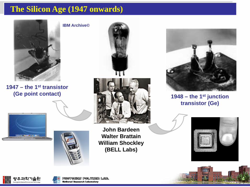
John BardeenWalter Brattain
William Shockley(BELL Labs)
1947 – the 1st transistor(Ge point contact) 1948 – the 1st junction
transistor (Ge)
IBM Archive©
The Silicon Age (1947 onwards)
4
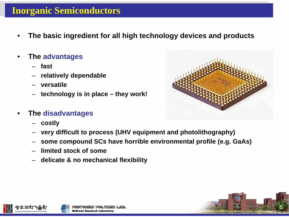
• The basic ingredient for all high technology devices and products
• The advantages– fast– relatively dependable– versatile– technology is in place – they work!
• The disadvantages– costly– very difficult to process (UHV equipment and photolithography)– some compound SCs have horrible environmental profile (e.g. GaAs)– limited stock of some– delicate & no mechanical flexibility
Inorganic Semiconductors
5

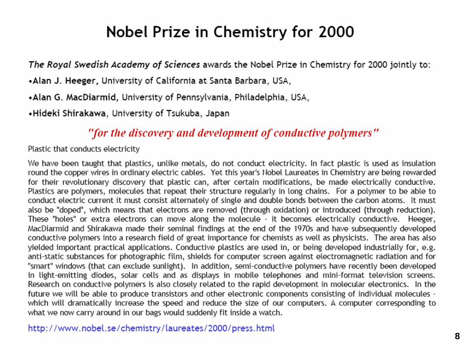
• The 2000 Nobel Prize for Chemistry was awarded for the discovery of metal-like electrical conductivity in iodine-doped polyacetylene
• Prior to this discovery (Shirakawa, Heeger, MacDairmid), it was thought that organic polymers could not conduct electricity in the solid state
• The “Soft Age” was born
A revolution in functional materials for high technology ?
The Soft Age (1977 to …. ?)
6

7
8

Organic Materials
9

• Explosion in “functional” soft-solids research (small molecule and large molecule organic electronics)
• Wild predictions of high tech and low tech applications – soft-solid related material benefits plus electrical (semiconducting) functionality
• IBM, Lucent, Philips, Seiko Epson, HP all have major organic electronics programs
A thin film conductingpolymer transistor and“soft-circuitry” – arraysof these transistors on
a flexible polymer sheetLight emitting polymerdisplays – thin, flexiblescreens with 180˚ view
plastic memorysmart textilesbiosensors
electronic inkorganic solar cells
Plastic Logic©
1,888 Transistors!
The Soft Age (1977 to …. ?)
10

12
Printed Electronics Markets
Printed electronics will be much bigger than the silicon chip market
Market forecast by component type for 2008 to 2018 in US $ billions, for printed and potentially printed electronics including organic, inorganic and composites
Source IDTechEx

Roadmap, Nikkei Electronics, March, 2007
Printed Electronics Technology Roadmap
13
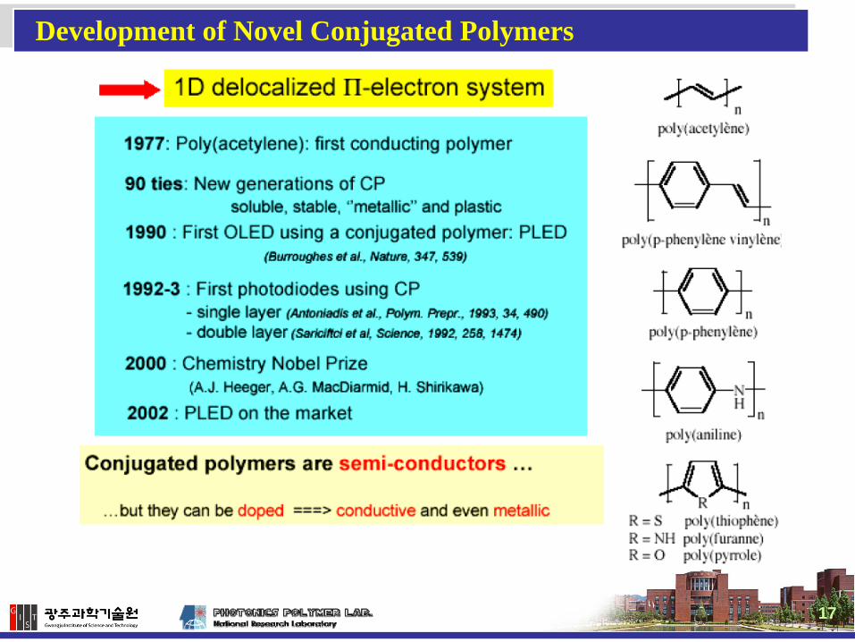
Development of Novel Conjugated Polymers
17
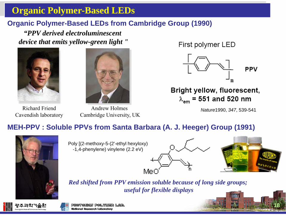
Organic Polymer-Based LEDs from Cambridge Group (1990)“PPV derived electroluminescent
device that emits yellow-green light "
Richard FriendCavendish laboratory
Andrew Holmes Cambridge University, UK
Nature1990, 347, 539-541
Organic Polymer-Based LEDs
Poly [(2-methoxy-5-(2'-ethyl hexyloxy)-1,4-phenylene) vinylene (2.2 eV)
Red shifted from PPV emission soluble because of long side groups; useful for flexible displays
MEH-PPV : Soluble PPVs from Santa Barbara (A. J. Heeger) Group (1991)
18

A polymer needs to show fluorescence
and to conduct electricity
to be a light emitting polymer
Light Emitting Polymers Convert Electric power into
visible light
Light-Emitting Polymers
19
14
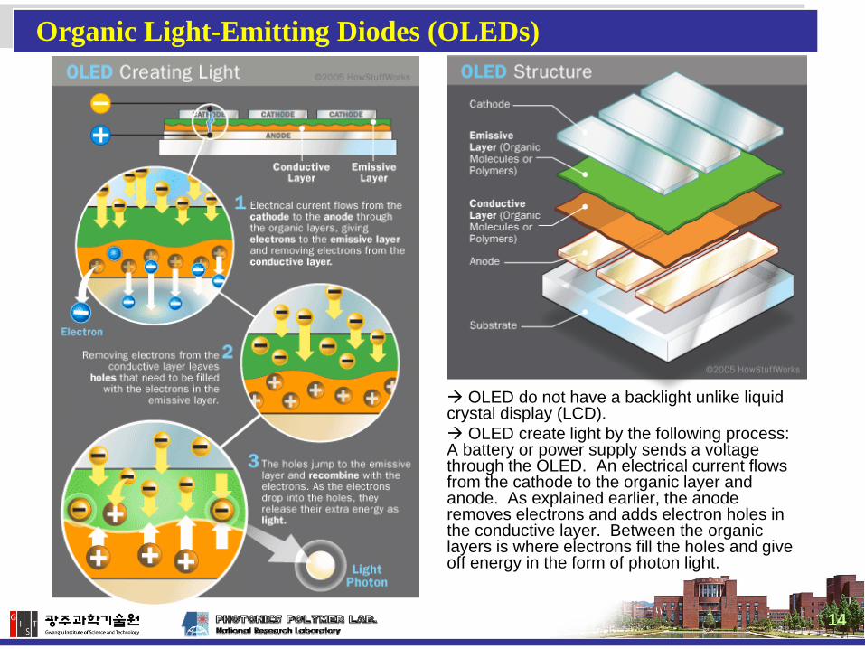
OLED do not have a backlight unlike liquid crystal display (LCD).
OLED create light by the following process: A battery or power supply sends a voltage through the OLED. An electrical current flows from the cathode to the organic layer and anode. As explained earlier, the anode removes electrons and adds electron holes in the conductive layer. Between the organic layers is where electrons fill the holes and give off energy in the form of photon light.
Organic Light-Emitting Diodes (OLEDs)

15
Organic Light-Emitting Diodes (OLEDs)
Flexible Display Research Trend
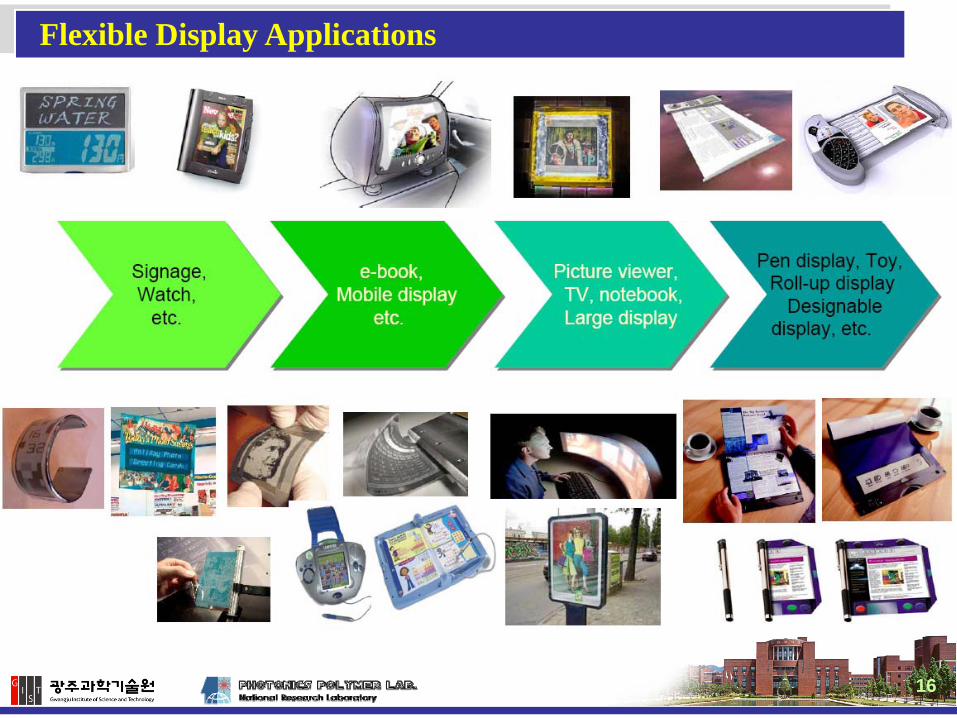
16
Flexible Display Applications

20
Electrochromic Display

21
Electrophoretic Display

22
E-Ink Flexible Display

Solar CellLight energy (photons) Electrical energy
-0.5 -0.4 -0.3 -0.2 -0.1 0.0-0.02
0.00
0.02
0.04
0.06
0.08
0.10
0.12
0.14
0.16
0.18
Cur
rent
(mA
)
Voltage (V)•
•
VOC
ISC
Pmax
32

33
Radiant power at Earth’s surface~ 100000 TW
Electricity consumption ~2 TW~ 80% from fossil fuels & nuclear, ~0.05% from PVAt 10% power conversion efficiency, solar resource can meet demand with 0.02% of Earth surface areaPV is the only technology to convert solar power directly into electricity
The Solar Energy Resource
3.7 GW installed by end 2005
Present PV system costs:– 7 - 20 Euro/Wp off-grid applications.– 4 - 8 Euro/Wp grid-connected.– Module 2 – 4 Euro / Wp
Aim for:– 1 - 2 Euro/Wp for power generation– 4 - 10 Euro/Wp for smaller applications.
Cost of Si based system falling through economies of scaleTo accelerate cost reductions, need technological innovations
PV Market Growth
33
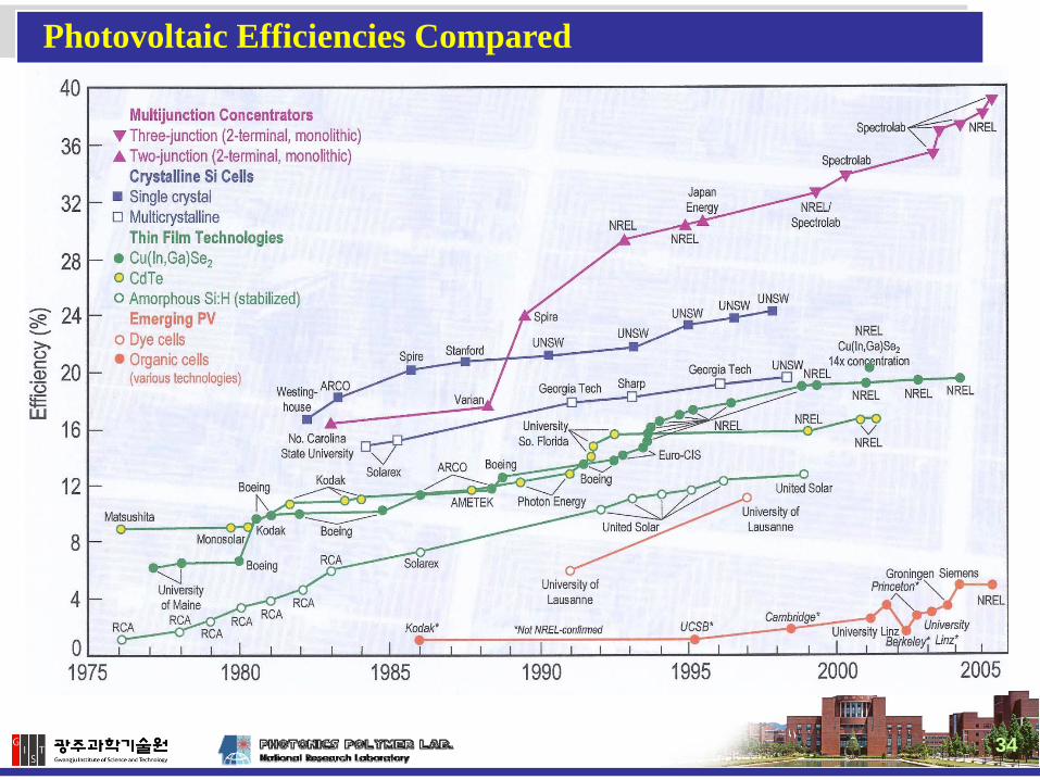
34
Photovoltaic Efficiencies Compared

35
Strategies to cost reduction
Use less photovoltaic material ?
Use cheaper photovoltaic materials and
fabrication process ?More work
per photon ?
Organic thin film materialsPrinting Technology
Molecular PV materials
Multijunction or “tandem” structuresExtracting more work
per photon
Concentration of sunlightLight trapping
Strategies to Cost Reduction
35

C60 CP
Bulk Heterojunction OPVs
36

37
Operation Principle of Fullerene Organic Photovoltaics

OPV benefits from the opportunities of renewable energies butoffers distinct competitive advantages
Pros & Cons of Photovoltaics
Organic Photovoltaics (OPVs)
38
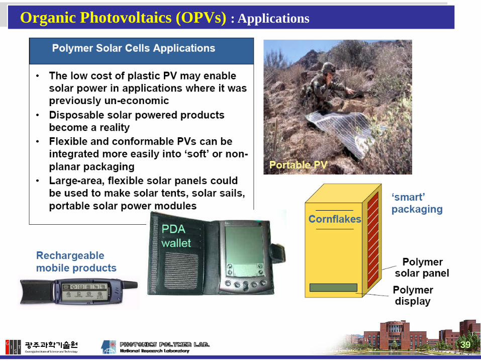
Organic Photovoltaics (OPVs) : Applications
39
40
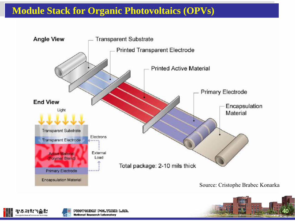
Source: Cristophe Brabec Konarka
Module Stack for Organic Photovoltaics (OPVs)

41
Voltage
Cur
rent
den
sity
J
Silicon
Best h 24%
Organic solar cellBest h ~4-5%
400 500 600 700 800 900 1000 1100 1200 13000
1
Irrad
ianc
e /W
m-2nm
-1
W avelength / nm
Electronacceptor
Electrondonor
Maximum eVoc
Key Challenges for Organic Photovoltaics (OPVs)
41
24
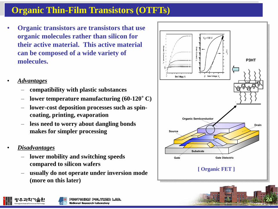
Organic Thin-Film Transistors (OTFTs)
• Organic transistors are transistors that use organic molecules rather than silicon for their active material. This active material can be composed of a wide variety of molecules.
• Advantages– compatibility with plastic substances– lower temperature manufacturing (60-120° C)– lower-cost deposition processes such as spin-
coating, printing, evaporation– less need to worry about dangling bonds
makes for simpler processing
• Disadvantages– lower mobility and switching speeds
compared to silicon wafers– usually do not operate under inversion mode
P3HT
[ Organic FET ]

25
Organic Thin-Film Transistors (OTFTs) Applications
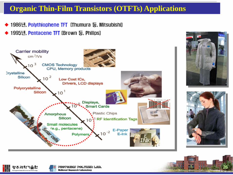
26
Organic Thin-Film Transistors (OTFTs) Applications

27
RFID for Item Level Tagging
Organic Thin-Film Transistor (OTFT)Basic Element of Organic Integrated Circuit
Ring OscillatorInverter
P-Channel & N-Channel OTFTs
Printed RFID Tags
O O
SS
O O
O O
SS
O O+
O O
Sn
SO3-
n
HSO3
m
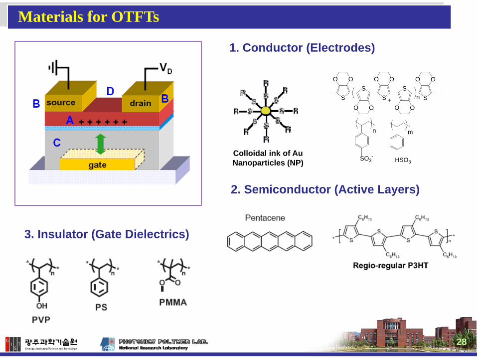
1. Conductor (Electrodes)
2. Semiconductor (Active Layers)
3. Insulator (Gate Dielectrics)
Materials for OTFTs
Colloidal ink of Au Nanoparticles (NP)
28

Small molecules (SMs) SMs, polymers
Reproducibility of properties
Monocrystalline Polycrystalline Amorphous solids
Luminescent property
Environmentalstability
Mechanicalstability
Electrical properties (mobility)
moderate very high, low very high
low moderate high
moderate high, moderate high
polymers
very low low, moderate high
very good good, moderate moderate to poor
pBTTT
Organic Semiconductors for OTFTs
29

μ = 0.6 cm2/Vs
μ = 0.1 cm2/Vs
μ = 0.007 cm2/Vs
μ = 0.01 cm2/Vs
μ = 1-5 cm2/Vs
μ = 15-20 cm2/Vs
μ = 0.1-1 cm2/Vs
• Significant progress in performance / reliability in recent years, but mobility still limited to 0.1 – 1 cm2/Vs.
n-channelp-channel
0.03 - 0.05 cm2V-1S-1
(1998, Vacuum Deposition)
~ 6 cm2V-1S-1
(in Vacuum)
0.01 - 0.05 cm2V-1S-1
Relatively low field-effect mobility and air stability compared to p-channel materials
Organic Semiconductors for OTFTs
30
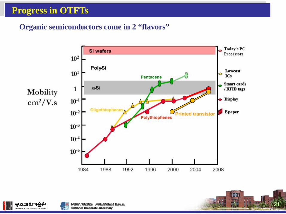
Printed transistor
Progress in OTFTs
Organic semiconductors come in 2 “flavors”
31

42
Organic Memory : Advantages and Applications
• Large area fabrication with extremely low cost
• Light-weight and flexibility
• High capacity with bottom-up stacking
• Capable ubiquitous componentsthat are printed onto plastic, glass or metal foils
: Inexpensive data storage media
: Disposable, mobile, flexible and low-duty applications.
Ex.) RFID tag, smart card, e-paper, OLED driving circuit, etc.
□ Advantages
□ Applications
ITRS 2005 – Emerging Research Devices
Technology Performance Evaluation(Polymer Memory)

43
Organic Memory: Research Approaches
OFET-Type Memory
[R.C.G. Naber, Nature Mater., 2005, 4, 243.]
- Ferroelectric polymer insulator- Polarizable gate dielectrics
Electrical Bistable Device
[Y. Yang, Appl. Phys. Lett. 2002, 80, 2997.]
AIDCN (2-amino-4, 5-imidazoledicarbonitrile)
- Electrical Biatability of Organic Semiconductor layer or MetalNano-particles, etc.
Hybrid Memory
[S. Möller, Nature, 2003, 426, 13.]
- In Combination of Inorganic andOrganic Materials

© www.wag.caltech.edu
© http://www.unibas.ch/phys-meso
Organic Materials to Nanotechnology : Scale without size
44

Graphite
Chris Ewels (www.ewels.info)
Conductivity:
Electrical Resistivity (ohm.m)perpendicular to c-axisparallel to c-axisnatural
9.8x10⁻⁶
4.1x10⁻⁵
1.2x10⁻⁶
Single-layer graphene transistor
Organic Materials to Nanotechnology : Graphene
45

Roll-up ofGraphite mesh
www.surf.nuqe.nagoya-u.ac.jp/.../ nanotubes.html
Organic Materials to Nanotechnology : Cabon Nanotube
46