materials in 2-dimension and beyond - nanyang · pdf file · 2013-02-05second...
TRANSCRIPT
Materials in 2-dimension and beyond
Philip Kim
Physics Department, Columbia University
Lecture III

Second Lecture: Friday 2/1,
morning
Spin and pseudospin in graphene
First Lecture: Thursday 1/31, afternoon
Bloch, Landau, and Dirac: Hofstadter’s Butterfly in Graphene
Third Lecture: Friday 2/1, afternoon
Materials in 2-dimension and beyond
School on Modern Topics in Condensed Matter Physics, Jan 31- Feb 1st, 2013, Singapore Philip Kim, Department of Physics, Columbia University
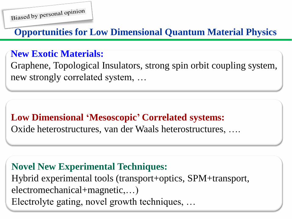
Opportunities for Low Dimensional Quantum Material Physics
New Exotic Materials:
Graphene, Topological Insulators, strong spin orbit coupling system,
new strongly correlated system, …
Low Dimensional ‘Mesoscopic’ Correlated systems:
Oxide heterostructures, van der Waals heterostructures, ….
Novel New Experimental Techniques:
Hybrid experimental tools (transport+optics, SPM+transport,
electromechanical+magnetic,…)
Electrolyte gating, novel growth techniques, …

Assembly of Various 2D Systems
X
X
M
C
B
N
graphene
hexa-BN
Metal-Chalcogenide
M = Ta, Nb, Fe, Co, Mo, …
X = S, Se, Te, …
Bi2Sr2CaCu2O8-x
Charge Transfer Bechgaard Salt
(TMTSF)2PF6
Lead Halide Layered Organic
Semiconducting materials: WSe2, NbS2, MoS2, …
Complex-metallic compounds : TaSe2, TaS2, …
Magnetic materials: FeSe2, CoSe2 ,…
Superconducting: NbSe2, Bi2Sr2CaCu2O8-x, ZrNCl,… A
B
A C
A

graphene intercalant
Ca, K, …
FeCl3, AgCl3, …
Br2, I2, …
Graphite Intercalate

Toward Graphene Superconductor?
M. Calandra and F. Mauri PRB(2006)
Tc c
BaC6 : < 0.3 K 5.2 A
SrC6 : 1.65 K 4.9 A
CaC6 : 11.5 K 4.5 A
MgC6: ? 3.9 A (calc)
MgC6 ?
MgxCa1-xC6

Vapor Phase Intercalation of Few Layer Graphene
Bilayer FeCl3 Intercalate
0 100 200 3000.0
0.5
1.0
1.5
R (
)
T (K)
0 2 4 6 8 10 12 14 16 18 200.00
0.05
0.10
0.15
0.20
R (
)
T (K)
Tc ~ 10 K
N. Kim et al. Nano Letters (2011)
Ca Intercalate in Mesoscopic Graphite
N. Kim et al. (2011)
• minimum possible intercalate
• high carrier density (5x1013cm-2)
• mobility ~ 1200 cm2/V sec
• quantum oscillations
• potential 2D magnetism
N. Kim et al. (2012)
• Superconducting Transition @ 11 K
• Hall Carrier density (3x1013cm-2)
Few Layer Graphene

Electrochemically Aided Adsorption / Intercalation
Stage 1 Stage 4 Stage 2 Graphite
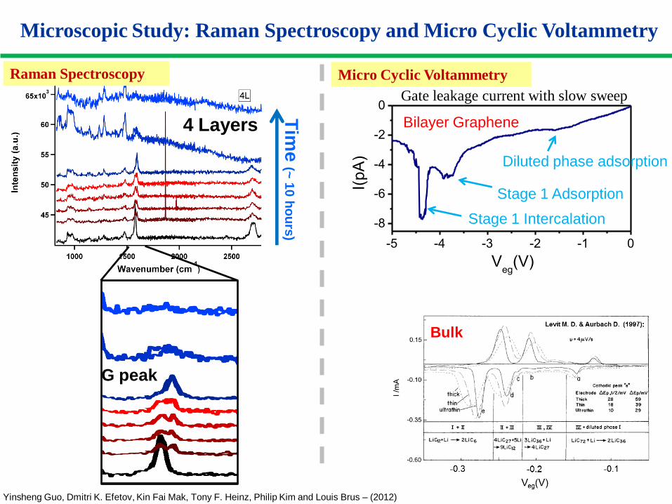
Li intercalation in few layer graphene in polymer electrolyte
Time (~ 10 hours)
Electrochemically Aided Adsorption Electrochemically Aided Intercalation
Yinsheng Guo, Dmitri K. Efetov, Kin Fai Mak, Tony F. Heinz, Philip Kim and Louis Brus – (2012)
-5 -4 -3 -2 -1 0
-8
-6
-4
-2
0
Veg
(V)
I(pA
)
Micro Cyclic Voltammetry
Bilayer Graphene
Gate leakage current with slow sweep
Bulk
Microscopic Study: Raman Spectroscopy and Micro Cyclic Voltammetry
Yinsheng Guo, Dmitri K. Efetov, Kin Fai Mak, Tony F. Heinz, Philip Kim and Louis Brus – (2012)
4 Layers
Tim
e (~
10 h
ou
rs)
G peak
Raman Spectroscopy
Diluted phase adsorption
Stage 1 Intercalation
Stage 1 Adsorption

Extremely High Carrier Density in Graphene
D. Efetov and P. Kim, Phys. Rev. Lett. (2010)
Polymer electrolyte: PEO+LiClO4
|n| < 1014 cm-2 ~
0 100 200
T (K)
r (
)
25
50
75
100
125
200
225

Controlling Bloch-Grueneisen Temperature
kF
kph
kF
kph ~ T
phonon sphere
electron sphere
kBTBG=2 hvs kF
D. Efetov and P. Kim (2010)
Ultimate limit of resistivity of
graphene at room
temperature ~20 / □

Multiband Transport in Bilayer Graphene
• Electrolyte Gating (Coarse Control)
~ 5x 1014 cm-2
• Back Gating (Fine Control)
~ 1013 cm-2
Hall measurement yields
the total density nH
Onset of the second subbands
Increased interband scattering Ve = -1.7 V Ve = -.4 V Ve = 1 V

Shubnikov de Haas Oscillations
1st subbands 2nd subbands 2nd subbands
Mobility of the second subband is much higher than that of first subbnad!
Multiband Transport in Bilayer Graphene
D. K. Efetov, P. Maher, S. Glinskis, and P. Kim Phys. Rev. B 84, 161412 (R)
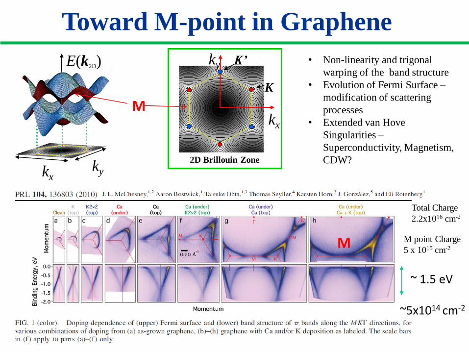
Toward M-point in Graphene
x
E(k2D)
kx ky
2D Brillouin Zone
kx
ky
K
K’
M
M
~ 1.5 eV
~5x1014 cm-2
• Non-linearity and trigonal
warping of the band structure
• Evolution of Fermi Surface –
modification of scattering
processes
• Extended van Hove
Singularities –
Superconductivity, Magnetism,
CDW?
Total Charge
2.2x1016 cm-2
M point Charge
5 x 1015 cm-2
-15 -10 -5 0 5 10 15
-30
-15
0
15
30
G2B2
G3E1
G4B3
G5B4
n
10
13cm
-2
Veg
V
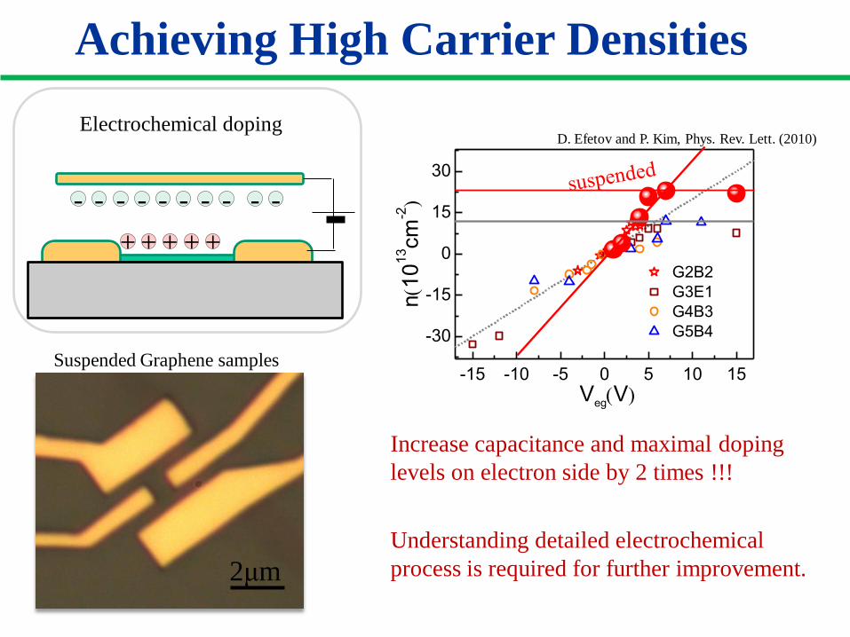
Achieving High Carrier Densities
-15 -10 -5 0 5 10 15
-30
-15
0
15
30
G2B2
G3E1
G4B3
G5B4
n
10
13cm
-2
Veg
V
Increase capacitance and maximal doping
levels on electron side by 2 times !!!
Understanding detailed electrochemical
process is required for further improvement. 2μm
Suspended Graphene samples
- - - - - - - - - -
+ + + + +
+ + + +
Gating from both sides of
suspended graphene samples D. Efetov and P. Kim, Phys. Rev. Lett. (2010) Electrochemical doping

Electrolyte Gating Sr2IrO4: Strongly Correlated Electrons
Samples: Ramesh group @ Berkeley
Sr2IrO2: Mott insulator with strong spin orbit coupling
-4 -3 -2 -1 0 1 2 30
20
40
60
80
100
Re
sis
tan
ce
(x1
03 W
)
Gate Voltage (V)
100 150 200 250 3001
10
100
1000 V
g = 0 V
Vg = -1 V
Vg = -2 V
Vg = -3 V
Vg = -4 V
Vg = -5 V
Re
sis
tan
ce
4w
ire (
kW
)
Temperature (K)
electron
doping
hole
doping
electron doping
• Ionic liquid doping of Mott insulator
• Metal-insulator transition in strong spin
orbit coupled Mott insulator
Ravichandran in progress (2012)

Co-lamination and
Vertical Heterostructures

Co-lamination and Transfer Techniques
1. spin coat substrate with PMMA and
scratch onto top surface
2. Lift off PMMA;
graphene comes with it!
3. Align graphene over target using a micro-
manipulator. PMMA is brought into contact
with target and annealed.
Collaboration: Hone and Shepard groups
Dean et al. Nature Nano (2010)

Flat Graphene on hBN
BN graphene
0.5 um
Roughness
-0.4 -0.2 0.0 0.2 0.40.0
0.4
0.8
1.2
Graphene
BN
fre
qu
en
cy [a
.u.]
height [nm]
0.22 nm
2 um

Room temperature mobility >100,000 cm2V-1s-1
Extremely High Mobility in Graphene/BN
Low temperature mobility >300,000 cm2V-1s-1
Platform for investigating extreme
quantum transport phenomena
Fractional quantum Hall states Hofstadter’s Butterfly Transport in Hydrodynamic Regime

Multi-Stacked Graphene Vertical Heterostructures
0 5 10 15 20 25-10
-5
0
5
10
RD
rag (
Ohm
s)
VBG
(Volts)
225 K
202 K
175 K
148 K
98 K
75 K
48 K
25 K
11 K
Temperature Dependent Coulomb Drag Effect
• Coulomb drag experiment high temperature
ranges for e-e and e-h interactions
• Coulomb drag, counter flow, and excitonic
transport at low temperatures
RXY
Counter flow
VBG (Volts)
VT
G (
Vo
lts)
Rxy (kOhm)
T = 20 mK
B = 20 T
Counter Flow Measurement
Dean et al., in progress (2012)

New Interfaces and
Transport Across
Heterostructures

Yang et al. (SAIT collaboration) Science 336, 1240 (2012)
Graphene/Silicon hybrid Device: Graphene Barristors
Gate Variable Schottky Diode
Invertor and half adder is demonstrated!

MoS2 / graphene Heterojunction
graphene MoS2 (3 nm)
10 mm SiO2
Si
MoS2
graphene
Graphene/MoS2 Schottky Junction
Barreiro et al. in preparation (2013)
Tunable Schottky Diode
-3 0 3-200
-100
0
100
Vg=40V
I (m
A)
V (V)
+V on MoS2
300K
Vg=-40V
-3 0 3-25
-20
-15
-10
-5
0
5
Vg=-30V
I (m
A)
V (V)
+V on MoS2
300K
Vg=-40V
Vg=+40V
Vg=-40V
Gate tunable MoS2/graphene junction
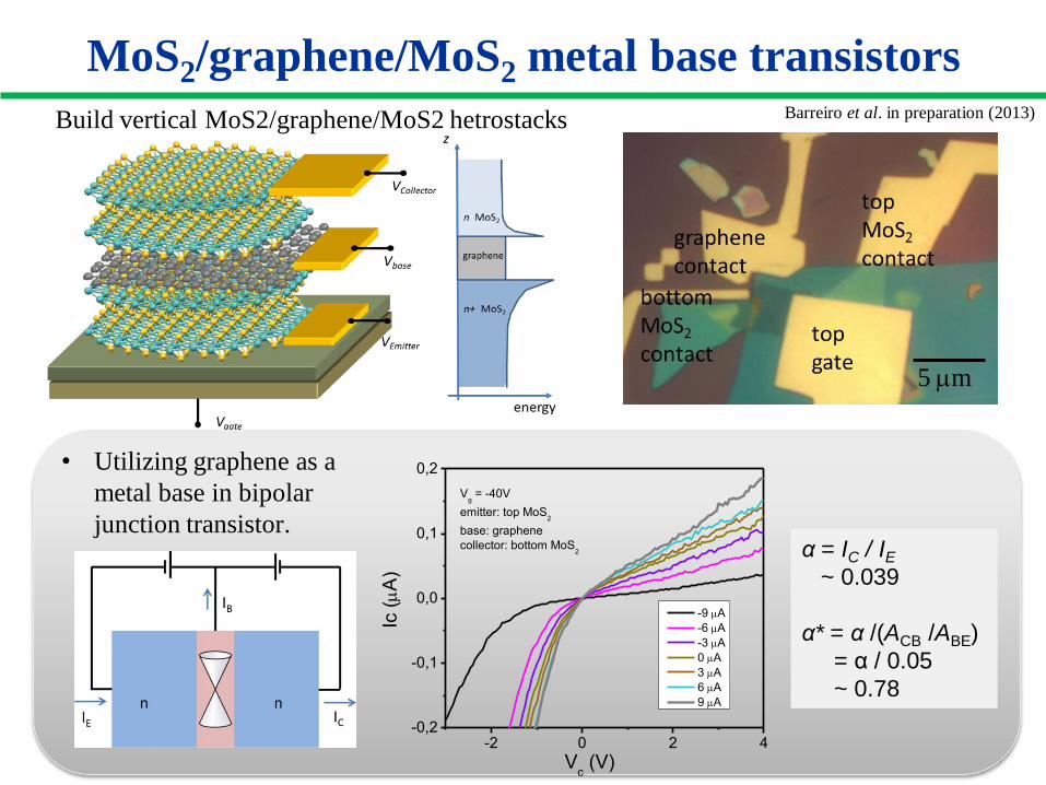
MoS2/graphene/MoS2 metal base transistors Barreiro et al. in preparation (2013)
5 mm
Build vertical MoS2/graphene/MoS2 hetrostacks
-2 0 2 4-0,2
-0,1
0,0
0,1
0,2
Ic (
mA
)
Vc (V)
-9 mA
-6 mA
-3 mA
0 mA
3 mA
6 mA
9 mA
Vg = -40V
emitter: top MoS2
base: graphene
collector: bottom MoS2
• Utilizing graphene as a
metal base in bipolar
junction transistor. α = IC / IE
~ 0.039
α* = α /(ACB /ABE)
= α / 0.05
~ 0.78

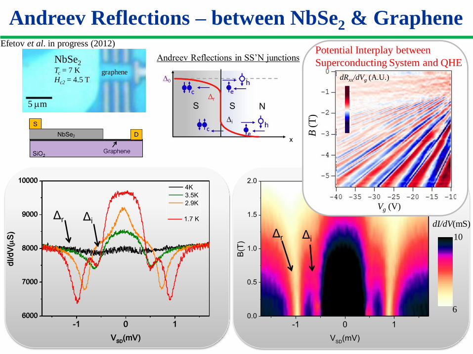
NbSe2/Graphene Heterostructures
Efetov et al. (2012)
NbSe2: quasi 2D superconductor
Superconducting transition
Tc = 7 K
Hc2 = 4.5 T
CDW transition
TcCDW= 33 K
-6 -4 -2 0 2 4 6
0.00
0.05
0.10
0.15
R(
)
B(T)
0 10 20 30 40 50
0.0
0.1
0.2
0.3
0.4
0.5
R(
)
T(K)
Tc = 7 K
TcCDW= 33 K
Hc2 = 4.5 T
Tc and Hc2 measurement in mesoscopic samples (~ 30 nm thick)
-1 0 10.0
0.5
1.0
1.5
2.0
B(T
)
VSD
(mV)
Δr Δi dI/dV(mS)
6
10
-1 0 16000
7000
8000
9000
10000
dI/
dV
(mS
)
VSD
(mV)
4K
3.5K
2.9K
-1 0 16000
7000
8000
9000
10000
1.7 K
dI/
dV
(mS
)
VSD
(mV)
Andreev Reflections – between NbSe2 & Graphene Efetov et al. in progress (2012)
Δr Δi
NbSe2 Tc = 7 K
Hc2 = 4.5 T
graphene
5 mm
Andreev Reflections in SS’N junctions
Vg (V)
B (
T)
dRxx/dVg (A.U.)
Potential Interplay between
Superconducting System and QHE

Van der Waals Epitaxy Growth vdW epitaxy can clean interface without chemical mismatch
t=32nm t=20nm
5μm
6~7μm
triangle
BiTe2 growth on hBN substrate
Collaboration with Moon group (Postech)
0 5 10 15
0.3
0.4
Rxx(K
)
B(T)
0.4
0.8
1.2
Rxy(K
)
0 2 4
-3
-2
-1
0
1
2
3
R-R
Poly
nom
ial f
it
1/B(T-1)
Shubnikov de Haas Oscillations
Magneto Resistance and Hall Resistance
Mobility
~ 1,000 cm2/Vsec
Rxx
Rxy
Ghahari et al (2012)

Rubrene on hBN with Graphene Electrodes
organic semiconductor
VG< 0
gate
Graphene source Grapahene drain
H-BN
VD
conducting channel at surface
– – – – – – – – – – – – – – – – – – ID
Graphene electrodes on BN
Rubrene Powder
Rubrene growth on hBN/ graphene
Chulho Lee et al (Nuckolls & Kim)
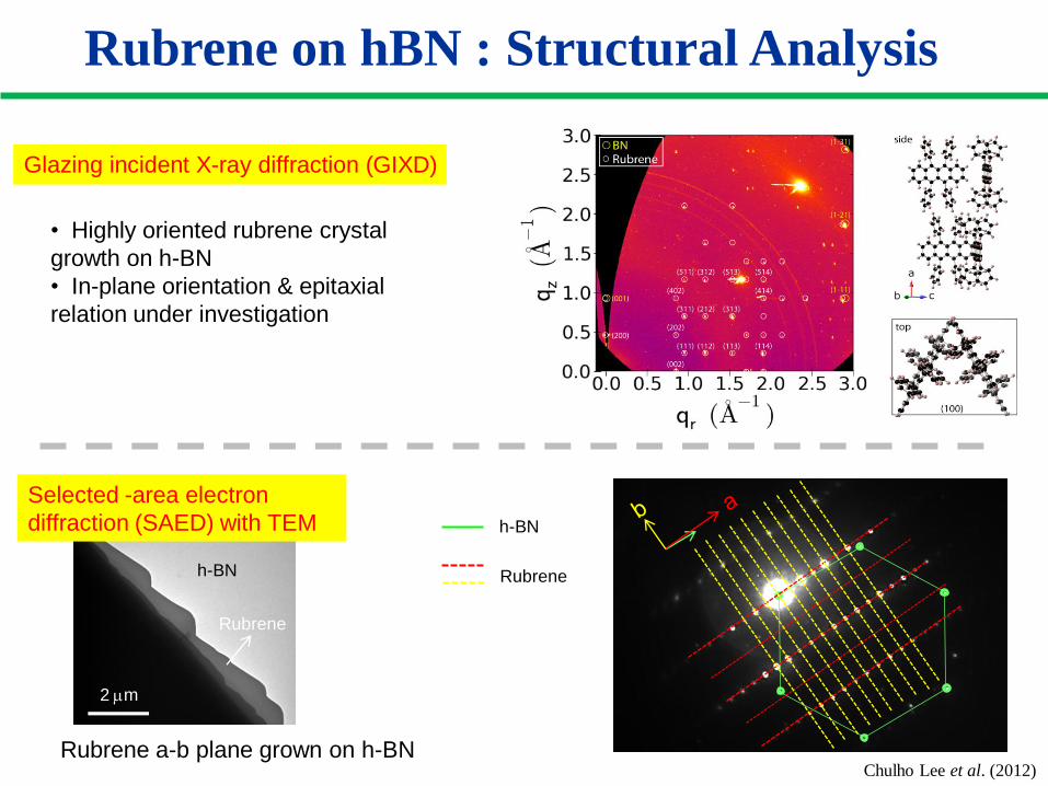
Rubrene on hBN : Structural Analysis
Chulho Lee et al. (2012)
Glazing incident X-ray diffraction (GIXD)
• Highly oriented rubrene crystal
growth on h-BN
• In-plane orientation & epitaxial
relation under investigation
2 mm
h-BN
Rubrene
Selected -area electron
diffraction (SAED) with TEM
Rubrene a-b plane grown on h-BN
h-BN
Rubrene

Rubrene on hBN with Graphene Electrodes: Transport
Chulho Lee et al. (2012)
20 mm
h-BN
CVD-graphene electrodes
20 mm
Rubrene grown on h-BN & graphene
-40 -30 -20 -10 0 10 20 301E-9
1E-8
1E-7
1E-6
1E-5
1E-4
VG (V)
-ID
S (
A)
VDS
= - 40 V
0.000
0.002
0.004
0.006
0.008
0.010
-I 1/2
DS (A
) 1/2
-40 -30 -20 -10 0-1.0x10
-4
-8.0x10⁻⁵
-6.0x10⁻⁵
-4.0x10⁻⁵
-2.0x10⁻⁵
0.0
-40 V
10 V
-30 V
-20 V
-10 V
0 V
20 V
I DS (
A)
VDS (V)
Mobility ~ 11.5 cm2/Vs
Low pressure growth
@ 200 C
Ohmic contact

Hybrid Experimental Tools

Combination of Scanning Probe/ Transport
• Transport
• Atomic force microscopy
• Scanning gate microscopy
• Scanning thermal microscopy
Scanning Kelvin probe microscopy
Y. Yu et al. (2011)

STM on Graphene/hBN
Spectroscopy Map in QHE regime

Mechanical Electromagnetic Measurements
Magnetization measurement
Electromechanical Devices: suspended graphene
Chen at al (2011)
Vikram et al (2012)
Direct experimental access of chemical potential!
(Deshpande et al, with Hone group collaboration)

Chemical Potential Measurement of Graphene Landau Levels
(Deshpande et al, with Hone group collaboration)
Chemical Potential Changes (simulation)
Spring constant (dynamic contribution)
kmag Fmag
z
m
nVg Cg
2
eA
Spring stiffening directly yields electronic compressibility n-2dn/dµ or DOS dn/dµ

(Deshpande et al, with Hone group collaboration)
Chemical Potential Measurement of Broken Symmetry QH States
• Broken Symmetry State
(n=1) are observed
• n=1 is measured to be
scale as B1/2 /
• Partially filled broken
symmetry LL provides
chemical potential
universal scaling of
)(/ nm Fv BF
Kravchenko et al. PRB (1990)

New Exotic Materials:
Graphene, Topological Insulators, strongly correlated system, …
Low dimensional ‘Mesoscopic’ correlated systems:
Oxide heterostructures, van der Waals heterostructures, ….
Novel New Experimental Techniques:
Hybrid experimental tools (transport+optics, SPM+transport,
electromechanical+magnetic,…)
Electrolyte gating, novel growth techniques, …
Summary

Acknowledgement
Funding:
Past Members
Melinda Han (Ph.D. 2010, Frontier of Science Fellow, Columbia University)
Meninder S. Purewal (Ph.D. 2008)
Josh Small (Ph.D. 2006)
Yuanbo Zhang (Ph.D. 2006, Professor, Fundan University)
Yuri Zuev (Ph.D. 2011, IBM Fishkill)
Kirill Bolotin (Assistant Professor, Department of Physics, Vanderbilt University)
Byung Hee Hong (Associate Professor, Department of Chemistry, Seoul National University)
Pablo Jarillo-Herrero (Assistant Professor, Department of Physics, MIT)
Keunsoo Kim (Assistant Professor, Department of Physics, Sejong University)
Namdong Kim (Research Scientist, POSTECH)
Barbaros Oezyilmaz (Assistant Professor, Department of Physics, National University of Singapore)
Current Members
Yue Zhao
Mitsuhide Takekoshi
Andrea Young
Dmitri Efetov
Fereshte Ghahari
Patrick Maher
Young-Jun Yu (jointly with GRL, POSTECH)
Vikram Deshpande (jointly with Hone group)
Paul Cadden-Zimansky (Columbia Frontier of Science Fellow)
Chenguang Lu (jointly with Hone and Herman
Collaborating Students/postodcs
Cory Dean, Inanc Meric, Lei Wang,
Sebastian Sorgenfrei, Kevin Knox, Nayung
Jung, Seok Ju Kang, Jun Yan, Yanwen Tan,
Kevin Knox
Collaborators
Horst Stormer, Aron Pinczuk, Tony Heinz, Abhay
Pasupathy, Latha Venkataraman
Louis Brus, George Flynn, Colin Nuckolls,
Jim Hone, Ken Shepard, Louis Campos, Rick Osgood
T. Taniguchi, K, Watanabe
Andre Geim, Kostya Novoselov, Sanka Das Sarma
Kim group and friends (2011)