materials science and engineering r - northeastern its · 2010-01-17 · controlled electron...
TRANSCRIPT

Q1
000
000
000
000
000
000
000
000
1
2
3
4
5678
91011
1213141516171819
Q3
n of
eate
iton
ina-
ces.
ovel
low
gies
plex
plex
rous
the
the
for
ved.
Q2 1, 2
e-40-
G Model
MSR 363 1–19
UN
CO
RR
EC
TED
PR
OO
FControlled electron injection and transport at materials interfaces in dyesensitized solar cells
V. Thavasi a,*, V. Renugopalakrishnan b, R. Jose a, S. Ramakrishna a,c,d,**a NUS Nanoscience and Nanotechnology Initiative (NUSNNI), National University of Singapore, Singapore 117576, Singaporeb Children’s Hospital, Harvard Medical School, 20 Shattuck Street, Boston, MA 02115, USAc Division of Bioengineering, National University of Singapore, Singapore 119260, Singapored Department of Mechanical Engineering, National University of Singapore, Singapore 119260, Singapore
Contents
1. Introduction . . . . . . . . . . . . . . . . . . . . . . . . . . . . . . . . . . . . . . . . . . . . . . . . . . . . . . . . . . . . . . . . . . . . . . . . . . . . . . . . . . . . . . . . . . . . . . . . . . . . .
2. Dye/metal oxide interface . . . . . . . . . . . . . . . . . . . . . . . . . . . . . . . . . . . . . . . . . . . . . . . . . . . . . . . . . . . . . . . . . . . . . . . . . . . . . . . . . . . . . . . . . .
2.1. Influence of dyes on electron injection . . . . . . . . . . . . . . . . . . . . . . . . . . . . . . . . . . . . . . . . . . . . . . . . . . . . . . . . . . . . . . . . . . . . . . . . . .
2.2. Effect of dye aggregation . . . . . . . . . . . . . . . . . . . . . . . . . . . . . . . . . . . . . . . . . . . . . . . . . . . . . . . . . . . . . . . . . . . . . . . . . . . . . . . . . . . . .
3. Role of metal oxide on the performance of metal oxide/dye interface . . . . . . . . . . . . . . . . . . . . . . . . . . . . . . . . . . . . . . . . . . . . . . . . . . . . . . .
3.1. Effect of electronic structure of metal oxides . . . . . . . . . . . . . . . . . . . . . . . . . . . . . . . . . . . . . . . . . . . . . . . . . . . . . . . . . . . . . . . . . . . . .
3.2. Effect of chemical stability of metal oxides . . . . . . . . . . . . . . . . . . . . . . . . . . . . . . . . . . . . . . . . . . . . . . . . . . . . . . . . . . . . . . . . . . . . . .
4. Effect of solvent environment . . . . . . . . . . . . . . . . . . . . . . . . . . . . . . . . . . . . . . . . . . . . . . . . . . . . . . . . . . . . . . . . . . . . . . . . . . . . . . . . . . . . . . .
Materials Science and Engineering R xxx (2008) xxx–xxx
A R T I C L E I N F O
Article history:
Available online xxx
Keywords:
Nanorods
Nanofibers
Nanowires
Energy conversion efficiency
Excitonic solar cells
Metal oxides
Electrolytes
Solvents effect
A B S T R A C T
Dye-sensitized solar cells (DSSCs) generate excitons (bound electron-hole pairs) upon absorptio
photon from the sunlight and undergo dissociation at the donor/acceptor materials interface to cr
free electrons and holes. Major challenges in DSSCs until now have been to achieve maximum exc
generation followed by dissociation, electrons injection and transportation with minimum recomb
tion, which are controlled by the dye/metal oxide, dye/electrolyte, and metal oxide/electrolyte interfa
Researchers have been focusing on improving these materials interfaces in DSSCs by using n
materials (doped metal oxides, wider spectral range dyes, and low viscous gel, ionic electrolytes and
molecular weight organic hole conductors), and introducing new semiconductor morpholo
(nanofibers, rods, wires, core–shell). With the current effort by researchers, TiO2/Ruthenium com
(N3 dye)-based liquid state DSSC have reached an efficiency of 11%, whereas TiO2/Ruthenium com
(N719 dye)/Solid electrolyte-based solid state DSSC have achieved an efficiency of �4%. As nume
materials have been the focal point in DSSCs, it is necessary to have an overall understanding on
materials interfaces and their influence on the performance of the solar cell. This review focuses on
metal oxides and metal oxide/dye interface that control the electron injection and transport
improving the efficiency of DSSCs.
� 2008 Elsevier B.V. All rights reser
* Corresponding author at: NUS Nanoscience and Nanotechnology Initiative (NUSNNI), National University of Singapore, Faculty of Engineering, Block E3, #05-1
Engineering Drive 3, Singapore 117576, Singapore. Tel.: +65 6516 6593; fax: +65 6872 5563.
** Corresponding author at: Division of Bioengineering, National University of Singapore, Singapore 119260, Singapore.
E-mail addresses: [email protected] (V. Thavasi), [email protected] (S. Ramakrishna).
Abbreviations: N3 dye, cis-di(thiocyanato)-bis(2,20-bipyridyl-4,40-dicarboxylic acid)-ruthenium(II); N719 dye, cis-di(thiocyanato)-bis(2,20-bipyridyl-4-carboxylat0 0 0 0
Contents lists available at ScienceDirect
Materials Science and Engineering R
journa l homepage: www.e lsev ier .com/ locate /mser
carboxylic acid)-ruthenium(II); N712 dye, (Bu4N)4[Ru(dcbpy)2(NCS)2]; Black dye, (C4H9)4N]3[Ru(Htcterpy)(NCS)3] (tcterpy = 4,4 ,4 -tricarboxy-2,2 ,2 -terpyridine); Z907
dye, cis-di(thiocyanato)-(2,20-bipyridyl-4,40-dicarboxylic acid)(4,40-dinonyl-2,20-bipyridyl)-ruthenium(II); Ru, ruthenium; SnO2, tin oxide; ZnO, zinc oxide; TiO2, titanium
oxide; Nb2O5, niobium oxide; In2O3, indium oxide; SrTiO3, strontium titanate; ZrO2, zirconium oxide; MgO, magnesium oxide; Al2O3, aluminum oxide; SiO2, silicon di oxide;
FTO, fluorine doped tin oxide; IPCE, incident photon conversion efficiency; h, solar-electric energy conversion efficiency; DMSO, dimethyl sulfoxide; AcN, acetonitrile; EtOH,
ethanol; Ace, acetone.
Please cite this article in press as: V. Thavasi, et al., Mater. Sci. Eng. R (2008), doi:10.1016/j.mser.2008.09.001
0927-796X/$ – see front matter � 2008 Elsevier B.V. All rights reserved.
doi:10.1016/j.mser.2008.09.001
5.
6.
7.
1. In
Tare(Si)cellsonggenetiveport
Din o(ii)electranmetin F
Tresumetredu
Dye
Rcoupdyeinjection
Dye
2021222324252627
28
29
3031323334353637383940414243444546474849
5051525354555657
Fig. 1Q4
elect
hole
2
G Model
MSR 363 1–19
Ple
UN
CO
RR
EC
TED
PR
OO
F
Effect of core–shell nanostructure . . . . . . . . . . . . . . . . . . . . . . . . . . . . . . . . . . . . . . . . . . . . . . . . . . . . . . . . . . . . . . . . . . . . . . . . . . . . . . . . . . . 000
Controlled electron transport by materials used in DSSCs. . . . . . . . . . . . . . . . . . . . . . . . . . . . . . . . . . . . . . . . . . . . . . . . . . . . . . . . . . . . . . . . . 000
6.1. Effect of 1D nanostructures for controlled electron transport . . . . . . . . . . . . . . . . . . . . . . . . . . . . . . . . . . . . . . . . . . . . . . . . . . . . . . . . 000
6.2. Effect of hybrid nanostructure. . . . . . . . . . . . . . . . . . . . . . . . . . . . . . . . . . . . . . . . . . . . . . . . . . . . . . . . . . . . . . . . . . . . . . . . . . . . . . . . . 000
6.3. Effect of nanodimensions. . . . . . . . . . . . . . . . . . . . . . . . . . . . . . . . . . . . . . . . . . . . . . . . . . . . . . . . . . . . . . . . . . . . . . . . . . . . . . . . . . . . . 000
Conclusion and future directions . . . . . . . . . . . . . . . . . . . . . . . . . . . . . . . . . . . . . . . . . . . . . . . . . . . . . . . . . . . . . . . . . . . . . . . . . . . . . . . . . . . . 000
Acknowledgements. . . . . . . . . . . . . . . . . . . . . . . . . . . . . . . . . . . . . . . . . . . . . . . . . . . . . . . . . . . . . . . . . . . . . . . . . . . . . . . . . . . . . . . . . . . . . . . 000
References . . . . . . . . . . . . . . . . . . . . . . . . . . . . . . . . . . . . . . . . . . . . . . . . . . . . . . . . . . . . . . . . . . . . . . . . . . . . . . . . . . . . . . . . . . . . . . . . . . . . . . 000
troduction
oday, the most successful solar photovoltaic devicesfabricated using semiconductor materials such as silicon[1]. In recent years, several alternatives to Si-based solar
have become available and considerable research isoing towards substantially reducing the cost of electricityration. Dye-sensitized solar cells (DSSCs) [2–4] are attrac-alternative as they can be inexpensive, light weight,
able and flexible.SSC possesses three major components: (i) dye sensitizerrder to harvest solar energy and generate excitons [5,6],
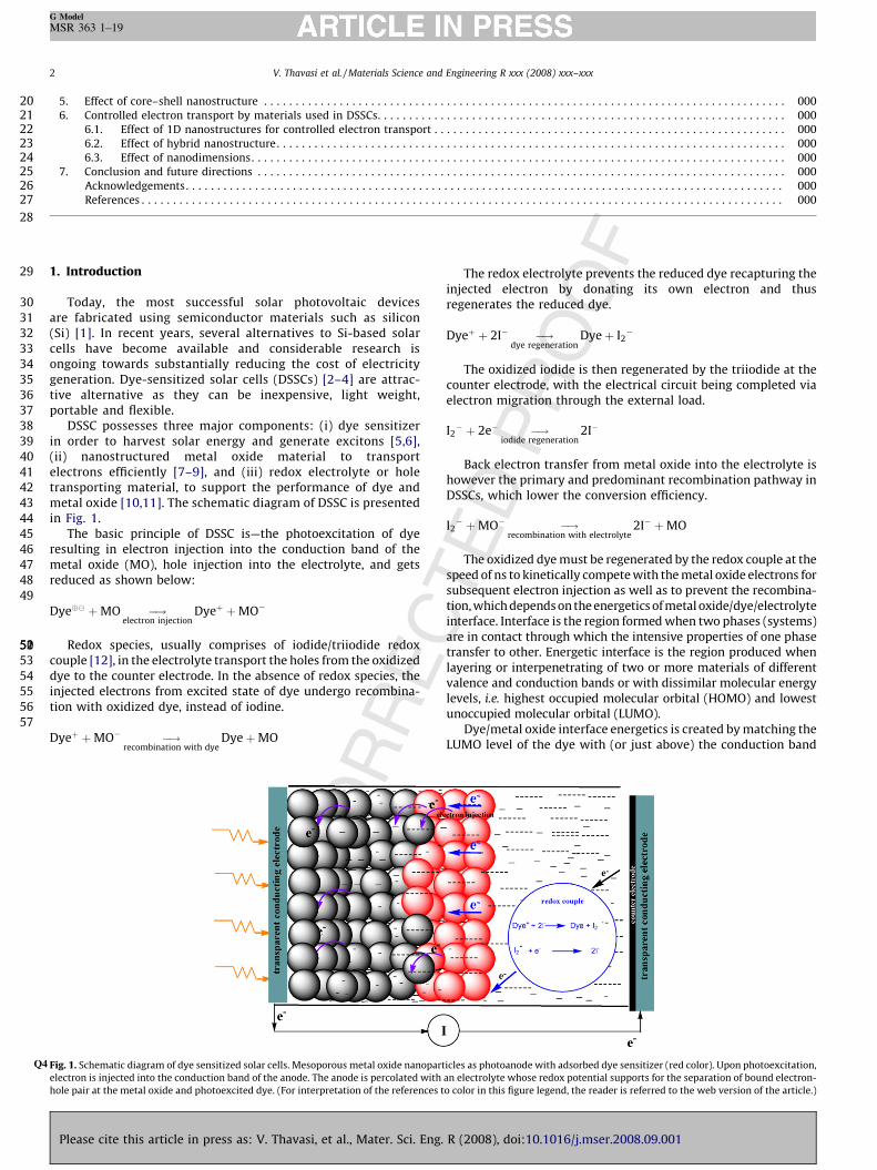
nanostructured metal oxide material to transporttrons efficiently [7–9], and (iii) redox electrolyte or holesporting material, to support the performance of dye andal oxide [10,11]. The schematic diagram of DSSC is presentedig. 1.he basic principle of DSSC is—the photoexcitation of dyelting in electron injection into the conduction band of theal oxide (MO), hole injection into the electrolyte, and getsced as shown below:
�� þMO �!electron injection
Dyeþ þMO�
edox species, usually comprises of iodide/triiodide redoxle [12], in the electrolyte transport the holes from the oxidized
to the counter electrode. In the absence of redox species, theted electrons from excited state of dye undergo recombina-with oxidized dye, instead of iodine.
þ þMO� �!recombination with dye
DyeþMO
The redox electrolyte prevents the reduced dye recapturing theinjected electron by donating its own electron and thusregenerates the reduced dye.
Dyeþ þ 2I� �!dye regeneration
Dyeþ I2�
The oxidized iodide is then regenerated by the triiodide at thecounter electrode, with the electrical circuit being completed viaelectron migration through the external load.
I2� þ 2e� �!
iodide regeneration2I�
Back electron transfer from metal oxide into the electrolyte ishowever the primary and predominant recombination pathway inDSSCs, which lower the conversion efficiency.
I2� þMO� �!
recombination with electrolyte2I� þMO
The oxidized dye must be regenerated by the redox couple at thespeed of ns to kinetically compete with the metal oxide electrons forsubsequent electron injection as well as to prevent the recombina-tion, which depends on the energetics of metal oxide/dye/electrolyteinterface. Interface is the region formed when two phases (systems)are in contact through which the intensive properties of one phasetransfer to other. Energetic interface is the region produced whenlayering or interpenetrating of two or more materials of differentvalence and conduction bands or with dissimilar molecular energylevels, i.e. highest occupied molecular orbital (HOMO) and lowestunoccupied molecular orbital (LUMO).
Dye/metal oxide interface energetics is created by matching theLUMO level of the dye with (or just above) the conduction band
V. Thavasi et al. / Materials Science and Engineering R xxx (2008) xxx–xxx
. Schematic diagram of dye sensitized solar cells. Mesoporous metal oxide nanoparticles as photoanode with adsorbed dye sensitizer (red color). Upon photoexcitation,
ron is injected into the conduction band of the anode. The anode is percolated with an electrolyte whose redox potential supports for the separation of bound electron-
pair at the metal oxide and photoexcited dye. (For interpretation of the references to color in this figure legend, the reader is referred to the web version of the article.)
ase cite this article in press as: V. Thavasi, et al., Mater. Sci. Eng. R (2008), doi:10.1016/j.mser.2008.09.001

d ofingthe
freen oftheandVOC
etalrgytheTheface
thed toted
tionherith
trolaretheandide,ace,
of
thetived ofnsi-ateseredye
ofThergyEex)
theintosferith
tate
ightdyethethebedt of
of
919293949596979899
100101102103104105106107108109110111112113114115116117118119120121122123124125126127128129130131132133134135136137138139140141
142143144145146147148149150151152153
3
G Model
MSR 363 1–19
UN
CO
RR
EC
TED
PR
OO
F
(ECB) of metal oxide. The dye/electrolyte interface is created suchthat the HOMO level of the electrolyte lies close to the HOMO levelof the dye for fast electron transfer, i.e. the ground-state oxidationpotential of dye must be sufficiently positive to oxidize the redoxcouple. The mass transfer rate of the redox species (I�/I3
�) has to besuperior, failing which results in higher electron-transfer resis-tance and lower conversion efficiency [13]. The ion mobility in theelectrolyte has been improved by adding additives: polymers [14–16], inorganic fillers [17–20] and plasticizers [20,21]. Lithiuminclusion in electrolyte has been commonly used in DSSCs, whereLi+ adsorbs onto the metal oxide surface and increases the chargeinjection efficiency of dye by shifting the conduction band edge tomore positive potentials [22,23]. Researchers have investigatedusing imidazolium cations in the electrolyte and noticed that theimidazolium cations adsorbs on the metal oxide surface and alignthe anion species due to electrostatic interaction, and therebyfacilitates electron transport [24]. By improving the ionic transportthe electron injection efficiency of dye can be enhanced; however,the control of ion composition (and concentration) should beoptimal for the higher performance of DSSCs.
The recombination could be minimized if: (i) the rate constantof electron injection from the excited dye into the conduction bandof metal oxide should be as small as possible, which dependsstrongly on the energetics of the metal oxide/dye/electrolyteinterface. Much of the current research in DSSC on global has beendevoted to the synthesis of dye sensitizers and experiment themon various metal oxides. The primary step to realize the maximumcharge injection into metal oxide is to dissociate the boundelectron-hole pairs (Frenkel excitons) generated upon photoexci-tation of dye [25], which depends on the energetics of dye/metaloxide interface. The dye/metal oxide interface is therefore one ofthe key issues to be addressed for obtaining higher energyconversion and retaining stability in the photoelectrochemicalenvironment. Therefore, for being significant in DSSC, the metaloxide/dye interface has been emphasized in this review. (ii)Following electron injection into the conduction band of metaloxide by photoexcited dye, electron collection at the collectingelectrode requires the transport of electrons in the nanoparticlesfilm to be faster before it undergoes recombination (back transfer),which depends on the nature and nanomorphology of metal oxide.In the nanoparticle film of 10 mm thick, an electron visitsapproximately 106 nanoparticles [26] on an average duringtransport before reaching the collecting electrode and plausiblethat such particles morphology acts as a potential recombinationsite. This review foresees the possibility of using one-dimensional(1D) nanomorphology by which such transport can be minimizedby achieving unidirectional transport.
The performance of each interface is crucial and have beendesignated using the parameters: open-circuit voltage VOC, fillfactor FF, and short circuit current density JSC, and expressed asefficiency (h) using the equation:
h ¼ VOCISCFF
Pinand FF ¼ ImaxVmax
ISCVOC
whereas VOC, is the maximum voltage obtained at zero current; ISC,the short circuit current is the maximum current obtained underless resistance (short circuit) conditions and Pin is the solarradiation intensity. Imax and Vmax are the maximum current andmaximum voltage, respectively. J (mA/cm2) depends on the
will be the FF. The electron injection into the conduction banmetal oxide results a dramatic increase in electron density, raisthe Fermi level towards the conduction-band edge. This shift ofFermi level of metal oxide under irradiation increases theenergy of injected electrons and is responsible for the generatiothe photovoltage in the external circuit. The VOC is related toenergy difference between the Fermi level of the metal oxidethe Nernst potential of the redox couple in the electrolyte. Theis influenced by the electronegativity (electron affinity) of moxide, and ionization potential of dye [27,28]. Raising the enelevel of the metal oxide conduction band should reducerecombination losses, and result in high open circuit voltage.suppression of dark current at the metal oxide/electrolyte interwill increase the VOC.
The maximum achievable theoretical efficiency (h) ofconversion of solar energy–electrical energy has been estimatebe 31% for DSSC [29], however, the highest demonstraefficiency so far has been only 11% [30]. Maximum charge injecand minimum recombination are the key to achieve higefficiency. Research has been focused on designing DSSC wvarious possible materials and their combination (Fig. 2). Conof electron injection and transport at the materials interfacescentral to the design of DSSCs. This review discusses onmaterials interfaces that influence efficient electron injectiontransportation, especially on three core elements (i) metal ox(ii) dye sensitizer, and (iii) metal oxide/dye/electrolyte interfwhich are primary determinants in the overall performanceDSSCs.
2. Dye/metal oxide interface
The dye/metal oxide interface is to be designed such thatoxidation potential of excited dye (LUMO) is sufficiently negato achieve efficient electron injection into the conduction banmetal oxide. Upon photon absorption, the dye molecule (setizer) reaches its excited energy state (LUMO) and generexcitons, which diffuse into the dye/metal oxide interface. Thwill be built-in energy gradient DE exists at the metal oxide/interface due to the energy difference between LUMO stateexcited dye and conduction band of metal oxide (ECB).electrons in the tightly bound excitons are so attracted by enegradient, and when this gradient exceeds the binding energy (of bound excitons, the exciton dissociation occurs:
As the energy level of freed electrons is equivalent toconduction state of metal oxide, ECB, the electrons are injectedmetal oxide, which is also called as forward electron tran(Fig. 3). LUMO of the excited dye therefore should be in-line wthe lower limit of the conduction band of metal oxide to facilithe effective electron injection into the metal oxide [2,31].
The amount of the sensitizer molecules available for lharvesting and charge injection are important upon adsorbingonto the metal oxide. Dye molecules are to be oriented onsurface of metal oxide with attachment functionalities ofmolecule. Orientation reduces the covering area per adsormolecule, providing a more compact and packed arrangementhe dye molecules, which allow for more adsorption dye
V. Thavasi et al. / Materials Science and Engineering R xxx (2008) xxx–xxx
itedande istheare
of
SC
charge injection and transport. To achieve larger JSC, the transportof electrons must be faster than the reaction with molecules in theelectrolyte. Hence, the JSC depends on the metal performance ofoxide/dye/electrolyte interface. FF is attributed to functioning ofthe metal oxide/electrolyte interface. The higher the recombina-tion of conduction band electrons with the electrolyte, the lower
Please cite this article in press as: V. Thavasi, et al., Mater. Sci. En
molecules. The rate constant for the migration of the excenergy would depend on the relative orientation of the donoracceptor moieties. However, this is no longer possible if the dyadsorbed as aggregates. Problem of poor electron transfer tometal oxide conduction band would be arisen if dyesaggregated that results in an unsuitable energetic position
g. R (2008), doi:10.1016/j.mser.2008.09.001

theinjecmetoxidthe dis thof enmetcoupthedistaprefmen
216217218219220221222223224225226227228
4
G Model
MSR 363 1–19
Ple
UN
CO
RR
EC
TED
PR
OO
F
LUMO level. Lower current density could be resulted by poortion efficiency, due to unfavourable binding of dye onto the
al oxide surface. The orientation of the molecule on the metale surface is characterized by the anchoring group present inye [32]. Anchoring groups of dye to the semiconductor surface
e most decisive factor help in bringing the relative orientationergy level of donor and acceptor during the attachment on the
al oxide and increase injection efficiency. The electronicling strengths differ depending on the relative position of
LUMO of the dye and its anchoring group [33]. The closernce between the anchoring group and the nearest LUMO is
erred for maximum and efficient electron injection. It is to betioned that the unique properties of dye sensitizer as well as
metal oxide affect electron injection when combined for formingdye/metal oxide interface [34]. In this part of review, the structuralinfluence of dye sensitizers, i.e. the effect of binding mode andnumber of anchoring groups while forming dye/metal oxideinterface on the electron injection efficiency are focused, whereason the metal oxides aspect, the chemical property and electronicstructure are discussed.
2.1. Influence of dyes on electron injection
Dye sensitizer bound via its electronically favorable bindingmode is preferable for enhancing electron injection efficiency.Metal oxide/dye interface in DSSCs is created by firmly grafting the
Fig. 2. Combination of materials and interfaces involved in DSSCs.
V. Thavasi et al. / Materials Science and Engineering R xxx (2008) xxx–xxx
Fig. 3. Schematic illustration of exciton dissociation at the metal oxide (TiO2)/dye interface and electron injection into metal oxide.
ase cite this article in press as: V. Thavasi, et al., Mater. Sci. Eng. R (2008), doi:10.1016/j.mser.2008.09.001
s itgeruldageioniO2.haslinkizerentits
cid.
etaltwoande or
ins into-
tingthe
ullyand
of44].fectiO2
ertyrgytedbertherceVOC
und
ronthation
240241242243244245246247248249250251252253254255256257258259260261262263264265266267268269270271272273274275276277278279280281282
5
G Model
MSR 363 1–19
UN
CO
RR
EC
TED
PR
OO
F
dye with its anchoring group such as carboxylic acid or phosphonicacid coordinated onto the metal oxide. Dyes anchored withphosphonic acid have demonstrated better long-term stabilityagainst moisture in the environment compared to carboxylic acidanchors which usually degrades upon absorption of moisture [35].However, the rate of electron injection from the dye via thecarboxylic group has been found almost twice when compared tobinding via the phosphonic anchor group [36]. Thus, largerphotocurrents can be obtained for dyes that link with its carboxylicacids [37]. Electron injection from higher excited states is mostlikely is vibrational in origin, i.e. hot electrons from the dye into themetal oxide and hence there is a mandatory requirement forproximal contact between the dye and metal oxide. This suggeststhat the dye–metal oxide distance should be shorter and thereforemode of linking of dye on metal oxide needs more attention.Previous researchers have found that the dye links onto TiO2
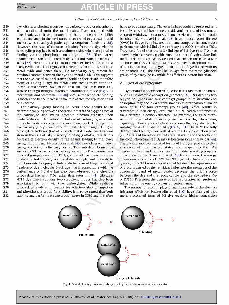
surface through bridging bidentate coordination mode (Fig. 4) ismore stable and preferable [38–40] because the bidentate bindingis shorter and hence increase in the rate of electron injection couldbe expected.
For carboxyl group binding to occur, there should be anelectronic coupling between the cationic metal and oxygen atom ofthe carboxylic acid which promote electron transfer uponphotoexcitation. The nature of linking of carboxyl group ontothe metal oxide also plays a role in enhancing electron injection.The carboxyl groups can either form ester-like linkages (C O) orcarboxylate linkages (C–O–O–) with metal oxide, via titaniumatom in the case of TiO2. Carboxyl binding (C–O–O–) results in adecrease of electron density of the ligand, leading to the lowerenergy shift in band. Nazeeruddin et al. [40] have observed higherenergy conversion efficiency for N3/TiO2 interface formed byanchoring N3 via two of their carboxylate groups. Due to numerouscarboxyl groups present in N3 dye, carboxylic acid anchoring byunidentate linking may not be stable enough, and it tends totransform into bridging or bidendate because of large rotationalfreedom of dye molecule. Black dye that is comparable with theperformance of N3 dye has also been observed to anchor viacarboxylate link with TiO2 rather than ester link [41]. Likewise,N719 dye which contains two carboxylic groups has also beenascertained to bind via two carboxylates. While realizingcarboxylate mode is important for effective electron injectionand phosphonate group for stability, it is to be noted that bothstability and performance are crucial issues in DSSC and therefore
have to be compensated. The ester linkage could be preferred ais stable (covalent like) on metal oxide and because of its stronelectron withdrawing nature, enhancing electron injection cobe obtained. Morakoshi et al. [42] have induced ester link(C O) in N3 dye by reflux treatment and compared its conversperformance with N3 linked via carboxylate (COO–) mode to TThey have found that the ester linkage of N3 dye onto TiO2
shows higher conversion efficiency than that of carboxylate-mode. Recent study has evidenced that rhodamine B sensitanchored on TiO2 via ester linkage (C O) delivers the photocurrof 2 orders of magnitude greater than that of dye linked withamide mode [41]. The ester-like linkage from the carboxylic agroup of dye may be favorable for efficient electron injection
2.2. Effect of dye aggregation
Dyes manifest poor electron injection if it is adsorbed on a moxide in unfavorable adsorption geometry [43]. N3 dye hasbipyridine ligands and four carboxyl groups in its structureadsorption may occur via several modes viz. protonation of onmore of all the four carboxyl groups [40], which resultsdifference in their energy levels that in turn lead to differencetheir electron injection efficiency. For example, the fully pronated N3 dye, while possessing an excellent light-harvescapability, shows poor electron injection efficiency due tomisalignment of the dye on TiO2 (Fig. 5) [31]. The LUMO of fdeprotonated N3 dye lies well above the TiO2 conduction b(�3.2 eV), and therefore excited state relaxation to the bottomthe conduction band of TiO2 may suffer from some energy loss [The di- and mono-protonated forms of N3 dyes provide peralignment of their excited states with respect to the Tconduction band and therefore manifest light-harvesting propat such orientation. Nazeerudin et al. [40] have obtained the eneconversion efficiency of 7.4% for N3 dye with four-protonagroups, but 9.3% for mono-protonated N3 dye. The larger numof protons carried by the sensitizer influences the energetics ofconduction band of metal oxide, decrease the driving fobetween the dye and the redox couple, and thereby reduceof DSSCs. Therefore, the degree of dye protonation has profoinfluence on the energy conversion performance.
The number of protons plays a significant role in the electinjection efficiency. Nazeerudin et al. [40] have observedmono-protonated form of N3 dye exhibits higher convers
V. Thavasi et al. / Materials Science and Engineering R xxx (2008) xxx–xxx
Fig. 4. Possible binding modes of carboxylic acid group of dye onto metal oxides surface.
Please cite this article in press as: V. Thavasi, et al., Mater. Sci. Eng. R (2008), doi:10.1016/j.mser.2008.09.001

efficafteTheydelivzerocleainfluhighpropconvachiN3 dbeensola0.75
TaggraggrshouelecwhiforsonisolvRapiaggrregemin
324325326327328329330331332333334335336337338339340341342343344345346347348349350351
6
G Model
MSR 363 1–19
Ple
UN
CO
RR
EC
TED
PR
OO
Fiency compared to the four, two, and zero proton sensitizersr examining N3/TiO2, N719/TiO2, and N712/TiO2-based DSSCs.
have observed that the mono-protonated N3-based DSSCers the JSC of 19 mA/cm2, whereas di-protonated N712 and
-protonated N719 showing 13 and 17 mA/cm2, respectively. Itrly emphasizes that the degree of protonation of the sensitizerences both JSC and VOC and therefore has to be optimized forer conversion efficiency of DSSC. Nazeeruddin et al. [40] hasosed that the one proton dye is the optimum for high-powerersion efficiency of the DSSCs. Other researchers have
eved 100% efficient electron injection from mono protonatedye into TiO2 [45]. Likewise, a conversion efficiency of 11.2% has
achieved for the mono-protonated N719/TiO2 interfacedr cell under AM 1.5 with 17.73 mA/cm2 JSC as 0.846 V, VOC asfor 0.158 cm2 cell [30].
he electron injection efficiency can also be influenced by theegation of dye molecules on the metal oxide surface. Lessegated or zero-aggregated dye anchoring onto the metal oxideld be desirable for faster electron injection. Dyes show slower
tron injection or self-quenching if it undergoes aggregation,ch can be encountered either before or during processing of dyeadsorption onto metal oxide. Processing methods such as
the process. However, another kind of aggregation of dye occursduring anchoring via intermolecular hydrogen bonding [43] andhence caution must be observed in the proper selection of dye forthe respective metal oxides. For instance, black dye (Fig. 6) hasbeen reported to form aggregates on the metal oxide surface due tothe long alkyl chain that undergoes hydrogen bonding duringanchoring and thereby affect the electron injection performance.Presence of numerous carboxyl groups also facilitates aggregation.Larger number of the carboxyl groups in the dye sensitizerincreases the electron-transfer efficiency due to their betteranchoring to the surface [47], however, numerous carboxyl groupscould offer steric hindrance which results in an uncoordinatedbinding onto the surface. Lesser the number of COOH groups, lowerthe possibility that it undergoes H bonding, and causes aggrega-tion. Z907 dye has lesser number of COOH groups in its structurewhich allows for well organized self-assembly onto the metaloxide surface. Hence, no self-quenching can be expected in Z907interfaced metal oxide (Fig. 7). The creation of energetic metaloxide interface with such dyes and with wide spectral coverageshould lead to higher energy conversion efficiency and stable DSSC.Even so, the dyes with one COOH group also cause slow electroninjection. For example, cyanine-based organic dyes L3 and L4
Fig. 5. Inefficient electron injection into metal oxide arises from misalignment and higher degree of protonation in N3 dye.
V. Thavasi et al. / Materials Science and Engineering R xxx (2008) xxx–xxx
cation or stirring that are used to dissolve the dye powder inent could cause dye aggregation upon excessive treatment.d method of interfacing dye with metal oxide form dyeegates that are less efficient in both electron injection and dyeneration by iodide [46]. This kind of aggregation can beimized quite easily by adopting precise engineering control on
ase cite this article in press as: V. Thavasi, et al., Mater. Sci. En
(Fig. 8) interface with TiO2 have caused poor injection efficiency,most likely originating from unfavorable binding or orientation ofthese dyes onto the TiO2 surface [48]. It is important to stress thatthe factors such as orientation, nature of binding, and structure ofthe dyes influence electron injection efficiency and therebyenhance overall performance of DSSC.
g. R (2008), doi:10.1016/j.mser.2008.09.001
d in59].for
tantthenic
e in
theor-
tiontionThed p)ty d
s sp
r ofon-msthefortheTheandype
benO/
380381
382383384385386387388389390391392393394395396397398399400401402403404405406407408409
7
G Model
MSR 363 1–19
UN
CO
RR
EC
TED
PR
OO
F
3. Role of metal oxide on the performance of metal oxide/dyeinterface
A schematic of energy level diagram describing the chargetransfer processes involved in DSSC is shown in Fig. 9. Electroninjection from dye sensitizer usually occurs in ultrafast time scaleand followed by a slower time scale, which have been denoted asfast and slow components, respectively, using biphasic (two-state)model [49,50]. The fast and slow components are attributed toinjection from unthermalized and relaxed excited states of dye,respectively (Fig. 9). It is to be noted that the rate of electroninjection is significantly contributed from unthermalized excitedstate (i.e. fast component) and play major role in the electroninjection efficiency. For N3/TiO2 system, the rapid electroninjection from N3 into TiO2 has occurred within 250 fs [44],whereas for N3/ZnO system, the injection time scales for fastcomponent has been estimated to be 1.5 ps [51]. For N3/SnO2
system, the electron injection speed have been found even slower,i.e. 5–10 ps [52–54].
For the invariant LUMO value of N3 dye, but for different metaloxides it has been found that the injection speed differs, suggestingthat metal oxide energetics could play a role. Energetically, theconduction band edge value (ECB) and band gap are similar for TiO2
and ZnO [55–57]. For the same LUMO level of N3 and with similarenergy values of TiO2 and ZnO, it is reasonable to expect the similarrate of injection. Nevertheless, the electron injection has beenfound faster in the case of N3/TiO2 that that of N3/ZnO. Likewise, onthe basis of energetics, SnO2 is expected to provide better electroninjection rate compared to TiO2 since its ECB edge position is 0.5 Vlower than that of TiO2 (see Fig. 9 and Table 1). The rate of electroninjection has been however slower than TiO2. Overall, the injection
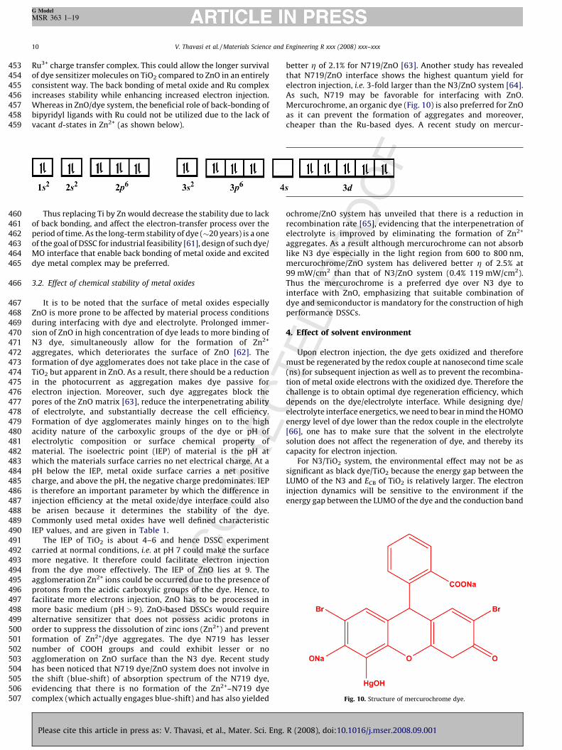
efficiency for the widely studied metal oxides has been founthe following order: TiO2 > Nb2O5 > SnO2 � ZnO � SnO2 [58,The energetic difference in metal oxides is unable to accountthe orders of magnitude difference in injection rate. An imporaspect that distinguishes metal oxides among each other iselectronic structure, and hence researchers have taken electrostructure of metal oxides into account to explain the differencinjection and performance.
3.1. Effect of electronic structure of metal oxides
According to Marcus theory of interfacial electron transfer,rate of electron injection under nonadiabatic condition is proptional to the density of accepting states (DOS) in the conducband of semiconductor. Electronic structure of the conducband is usually comprised of empty s, p, d and f orbitals.conduction band of SnO2 is composed primarily of empty s (anorbitals of Sn4+, whereas TiO2 is composed primarily of emporbitals of Ti4+. The d bands are typically narrower, whereabands are broader and having density of states (DOS) an ordemagnitude smaller than d-type conduction bands. The electrtransfer integrals for the d-orbitals of the neighboring metal atoare smaller than that of the integrals for s-orbitals. Therefore,effective mass (me) of the conductive electron should be largerd-orbital materials. When the effective electron mass is larger,DOS near the conduction band edge also becomes larger.electron effective mass in d-type conduction bands (5–10 me3 me for TiO2 and Nb2O5, respectively) is higher than i-tconduction bands (0.3 me for SnO2 and ZnO). This couldattributed for slower electron injection rate at SnO2/dye and Zdye interfaces compared to TiO2/dye interface.
Fig. 6. Structure of black dye.
Table 1Properties of metal oxides that influence the performance of dye/metal oxide interface.
Material Isoelectric
point
Band gap ECB = 0.0 V versus NHE Electron
affinity
Density of states
(effective electron mass)
Electronic structure
V. Thavasi et al. / Materials Science and Engineering R xxx (2008) xxx–xxx
Anatase TiO2 5–6 3.3 0.5 V 3.9 eV 5–10 me d orbitals of Ti4+ density of
states is higher than others
ZnO 4–9 3.3 Close to TiO2 �0.5 V higher than SnO2 4.5 eV 0.3 me s, p orbitals of Zn2+
SnO2 2.5–4.0 3.5 0.5 V lower than TiO2 4.8 eV 0.3 me s and p orbitals of Sn4+
In2O3 7.1 3.6 0.5 V lower than TiO2 4.45 eV 0.3 me s orbitals of In3+
Nb2O5 2.6–4.5 3.4 0.2–0.3 eV higher than TiO2 2.34 eV 3 me d orbitals of Nb5+
Please cite this article in press as: V. Thavasi, et al., Mater. Sci. Eng. R (2008), doi:10.1016/j.mser.2008.09.001

Ueleccontstru
TTiO2
bon
439440441442
443444445
8
G Model
MSR 363 1–19
Ple
UN
CO
RR
EC
TED
PR
OO
F
pon photoexcitiation, the Ru dye complex transfer thetronic charge density first to ligand orbital which is in intimateact with the conduction band of the TiO2. For Ti4+, the orbitalcture is as follows:
strength of p orbitals of ligand. The electron injection from theligand goes into the vacant t2g orbital as the excited electrondonating ð* orbitals match with the ð symmetry t2g d orbitals ofTi4+ atoms, and reducing it to Ti3+. Overall, the substantial increase
Fig. 7. Well organized self-assembly of Z907 dye onto the metal oxide prevents aggregation and self-quenching.
V. Thavasi et al. / Materials Science and Engineering R xxx (2008) xxx–xxx
he 3d orbitals of Ti4+ are near the conduction band edge of. The di-carboxyl bipyridyl ligand in dye molecule exerts back
ding with the Ru complex that actually enhances the acceptor
ase cite this article in press as: V. Thavasi, et al., Mater. Sci. En
in electron injection occurs from excited dye to TiO2 [60].Moreover, this phenomena enable a back bonding reaction,facilitating the formation of a temporary interfacial Ti3+–ligand–
g. R (2008), doi:10.1016/j.mser.2008.09.001

UN
CO
RR
EC
TED
PR
OO
FFig. 8. Cyanine-based organic dyes.
Fig. 9. Energy level diagram for metal oxide/dye/electrolyte interfaces.
V. Thavasi et al. / Materials Science and Engineering R xxx (2008) xxx–xxx 9
G Model
MSR 363 1–19
Please cite this article in press as: V. Thavasi, et al., Mater. Sci. Eng. R (2008), doi:10.1016/j.mser.2008.09.001
Ru3+
of dyconsincrWhebipyvaca
Tof bperiof thMOdye
3.2.
IZnOdurisionN3aggrformTiO2
in telecporeof eFormacidelecmatwhipHcharis thinjebeComIEP
Tcarrmorfromagglprotfacilmoralteordeformnumagglhastheevidcom
453454455456457458459
460461462463464465
466
467468469470471472473474475476477478479480481482483484485486487488489490491492493494495496497498499500501502503504505506507
10
G Model
MSR 363 1–19
Ple
UN
CO
RR
EC
TED
PR
OO
F
charge transfer complex. This could allow the longer survivale sensitizer molecules on TiO2 compared to ZnO in an entirelyistent way. The back bonding of metal oxide and Ru complex
eases stability while enhancing increased electron injection.reas in ZnO/dye system, the beneficial role of back-bonding ofridyl ligands with Ru could not be utilized due to the lack ofnt d-states in Zn2+ (as shown below).
hus replacing Ti by Zn would decrease the stability due to lackack bonding, and affect the electron-transfer process over theod of time. As the long-term stability of dye (�20 years) is a onee goal of DSSC for industrial feasibility [61], design of such dye/interface that enable back bonding of metal oxide and excitedmetal complex may be preferred.
Effect of chemical stability of metal oxides
t is to be noted that the surface of metal oxides especiallyis more prone to be affected by material process conditions
ng interfacing with dye and electrolyte. Prolonged immer-of ZnO in high concentration of dye leads to more binding ofdye, simultaneously allow for the formation of Zn2+
egates, which deteriorates the surface of ZnO [62]. Theation of dye agglomerates does not take place in the case ofbut apparent in ZnO. As a result, there should be a reduction
he photocurrent as aggregation makes dye passive fortron injection. Moreover, such dye aggregates block thes of the ZnO matrix [63], reduce the interpenetrating abilitylectrolyte, and substantially decrease the cell efficiency.ation of dye agglomerates mainly hinges on to the high
ity nature of the carboxylic groups of the dye or pH oftrolytic composition or surface chemical property oferial. The isoelectric point (IEP) of material is the pH atch the materials surface carries no net electrical charge. At abelow the IEP, metal oxide surface carries a net positivege, and above the pH, the negative charge predominates. IEPerefore an important parameter by which the difference in
ction efficiency at the metal oxide/dye interface could alsoarisen because it determines the stability of the dye.monly used metal oxides have well defined characteristic
values, and are given in Table 1.he IEP of TiO2 is about 4–6 and hence DSSC experimentied at normal conditions, i.e. at pH 7 could make the surfacee negative. It therefore could facilitate electron injection
the dye more effectively. The IEP of ZnO lies at 9. Theomeration Zn2+ ions could be occurred due to the presence ofons from the acidic carboxylic groups of the dye. Hence, toitate more electrons injection, ZnO has to be processed ine basic medium (pH > 9). ZnO-based DSSCs would requirernative sensitizer that does not possess acidic protons inr to suppress the dissolution of zinc ions (Zn2+) and preventation of Zn2+/dye aggregates. The dye N719 has lesser
better h of 2.1% for N719/ZnO [63]. Another study has revealedthat N719/ZnO interface shows the highest quantum yield forelectron injection, i.e. 3-fold larger than the N3/ZnO system [64].As such, N719 may be favorable for interfacing with ZnO.Mercurochrome, an organic dye (Fig. 10) is also preferred for ZnOas it can prevent the formation of aggregates and moreover,cheaper than the Ru-based dyes. A recent study on mercur-
ochrome/ZnO system has unveiled that there is a reduction inrecombination rate [65], evidencing that the interpenetration ofelectrolyte is improved by eliminating the formation of Zn2+
aggregates. As a result although mercurochrome can not absorblike N3 dye especially in the light region from 600 to 800 nm,mercurochrome/ZnO system has delivered better h of 2.5% at99 mW/cm2 than that of N3/ZnO system (0.4% 119 mW/cm2).Thus the mercurochrome is a preferred dye over N3 dye tointerface with ZnO, emphasizing that suitable combination ofdye and semiconductor is mandatory for the construction of highperformance DSSCs.
4. Effect of solvent environment
Upon electron injection, the dye gets oxidized and thereforemust be regenerated by the redox couple at nanosecond time scale(ns) for subsequent injection as well as to prevent the recombina-tion of metal oxide electrons with the oxidized dye. Therefore thechallenge is to obtain optimal dye regeneration efficiency, whichdepends on the dye/electrolyte interface. While designing dye/electrolyte interface energetics, we need to bear in mind the HOMOenergy level of dye lower than the redox couple in the electrolyte[66], one has to make sure that the solvent in the electrolytesolution does not affect the regeneration of dye, and thereby itscapacity for electron injection.
For N3/TiO2 system, the environmental effect may not be assignificant as black dye/TiO2 because the energy gap between theLUMO of the N3 and ECB of TiO2 is relatively larger. The electroninjection dynamics will be sensitive to the environment if theenergy gap between the LUMO of the dye and the conduction band
V. Thavasi et al. / Materials Science and Engineering R xxx (2008) xxx–xxx
Fig. 10. Structure of mercurochrome dye.
ber of COOH groups and could exhibit lesser or noomeration on ZnO surface than the N3 dye. Recent studybeen noticed that N719 dye/ZnO system does not involve inshift (blue-shift) of absorption spectrum of the N719 dye,encing that there is no formation of the Zn2+–N719 dyeplex (which actually engages blue-shift) and has also yielded
ase cite this article in press as: V. Thavasi, et al., Mater. Sci. Eng. R (2008), doi:10.1016/j.mser.2008.09.001

zedtheuld
atesthasthethedu-ialsthefor
hedughntothe
tionon-on/ent.69].alsos a
543544545546547548549550551552553554555556557558559560561562563564565566567568569570571572573574575
nger
11
G Model
MSR 363 1–19
UN
CO
RR
EC
TED
PR
OO
F(ECB) of metal oxide is smaller. For instance, the energy gapbetween the LUMO of black dye and the ECB of TiO2 is relativelysmall because LUMO of black dye is located just above theconduction band (ECB) of TiO2 [67] and, therefore electron injectionshould be sensitive to environment such as presence of additivesand solvent in the electrolyte. The electron injection from dyehas been found to be faster in acetonitrile (AcN), a dipolarsolvent when compared to polar protic ethanol (EtOH) and polaraprotic DMSO [68]. The rate of electron injection from dye intoTiO2 has been found to be in the following order;AcN > EtOH > DMSO. The difference in the electron injectionof dye in the solvent medium could be ascribed to the interactiveability of solvent. Electrolytic solvent molecules may engagethrough intermolecular interaction with the COOH group of dyemolecules and can intercept the dye’s electron injection in twopossible ways; (i) at excited state and (ii) at the oxidized state. Aslaid out in Fig. 11a the interaction of acetonitrile with the exciteddye is prevented or weakened due to the lower electronegativenature of N atom of acetonitrile. This may allow the excited dyeto release (inject) their electrons considerably faster into themetal oxide. This could also allow an additional pathway forelectron injection in the acetonitrile medium. Hence fasterinjection is observed in AcN mediated electrolyte. Higherelectronegative nature of O atom in solvents such as ethanoland acetone could exert stronger molecular interaction with thefunctional group of the dye (Fig. 11b) which will influence theexcited-state charge-transfer kinetics and energetics. As a result,
(Fig. 11c). The strong interaction with solvent at the oxidistate of dye could change the energetic level, restrictingacceptance of new electrons from the redox couple, which coslow down the subsequent injection.
5. Effect of core–shell nanostructure
Control of interfacial electron injection and recombinationthe metal oxide/dye/electrolyte interfaces is pivotal for the bperformance of DSSCs. Doping at the dye/metal oxide interfacereceived increased attention among researchers to improveinjection efficiency and suppress the recombination asinterfacial energetics can be controlled by this strategy. Introcing cations as dopant on the surface of photoanode mater(metal oxides) exerts larger dipole moment that changesinterface energetics in an energetically more favorable wayelectron transfer [69]. Recombination rate will be diminisbecause the doped cations could shield electron back flow thrometal oxide to the electrolyte. The doping of strontium ions othe TiO2 (i.e. SrTiO3) has been observed to shift the ECB innegative direction, i.e. from �4.1 to �3.7 eV [70,71]. Conducshift in the negative direction increases the efficiency of electrhole separation at the interface and reduces the electrelectrolyte recombination rate and thus increases photocurrThe reduction in the recombination rate results in larger VOC [Insertion of another metal oxide as shell or interface modifiercontrols the back electron transfer, as the shell layer form
Fig. 11. Effect of electrolyte solvents on the electron injection performance of dye; (a) N3 dye exhibits a weak interaction with acetonitrile, (b) N3 dye forms a stro
interaction with ethanol, (c) N3 dye forms a strongest interaction with DMSO.
V. Thavasi et al. / Materials Science and Engineering R xxx (2008) xxx–xxx
tionling
behanure
the electron injection is restricted, which could lead for theslower electron injection kinetics in EtOH. A very strongintermolecular attraction is expected between excited dye andlone pair oxygen atom of DMSO because of the strongestelectronegative nature of O atom, that could change theenergetics of the excited dye, results in slower injection rate
Please cite this article in press as: V. Thavasi, et al., Mater. Sci. En
surface energy barrier, which slows down the recombina[69,72–74]. If dethermalization of electron occurs upon travelin the matrix of the anode material, such electrons canabstracted by shell material, i.e. second metal oxide rather tbeing back injected into the electrolyte due to its lower ECB nat(Fig. 12).
g. R (2008), doi:10.1016/j.mser.2008.09.001

SdepoTiO2
reacshelrecocentcoatMgOphosuggrecolayehas(>3its lMgOintedecrthein JS
shelin TSiO2
fromgapsigncomthatof n(phobandelecmat
Ishelmak
607608609610611612613614615616617618619620621622623624625626627628629630631632633634635636637638639640641642643
12
G Model
MSR 363 1–19
Ple
UN
CO
RR
EC
TED
PR
OO
Feung Jae Roh et al. [75] have observed that the ZnO adsorbed/sited as shell material on TiO2 with a thickness of 30 nm at/N3 interface reduces electron-hole recombination andhes an efficiency of 4.51% at 80 mW/cm2. Presence of Al2O3
l layer on TiO2 [76] also has been observed to retard thembination dynamics by passivating surface recombinationers and decreasing the rate of back electron transfer. Al2O3-ed SnO2 has been reported to increase VOC. The presence of
as SnO2/MgO/N719 interface is observed to deliver a highertocurrent (JSC of 9.7 mA/cm2) [77], compared to SnO2/N719esting that the MgO is involved in the suppression of chargembination. The performance of shell material depends on theirr thickness at metal oxide/dye interface [78,79]. For example, itbeen noticed that ZnO shell layer with larger thickness
0 nm) leads to leakage of electrons to the electrolyte because ofow electron effective mass, 0.3 me [75]. Similarly, 1 nm thick
layer at SnO2/dye interface and 1 nm thick Al2O3 at TiO2/dyerface have resulted in 4-fold [80,81] and 3-fold [82,83]ease in the rate of recombination, respectively. Increasing
thickness of Al2O3 layer on TiO2 has resulted in larger decrease
C, but not much in FF and VOC, indicating that the thickness ofl layer mainly affects the electron transfer. The literature dataable 2 reveals that larger band gap materials: MgO, Al2O3, and
as shell layer have resulted in larger JSC, which could be ariselarger enhanced electron injection. Whereas smaller band
materials such as zirconia (ZrO2) and SrTiO3 have notificantly improved the photocurrent from TiO2/dye interfacepared to that of larger band gap materials. It has been noticedthe absorption spectrum of MgO-coated TiO2 is similar to thateat TiO2, evidencing that light absorption spectrum of coretoanode) material is not be affected by the presence of larger
which could change the electronic property of the core anodematerials. For example, the SiO2 as shell layer on TiO2 could modifythe electronic structure of the Ti atoms by forming Ti–O–Si bondsat the inter-phase boundary of TiO2–SiO2 interface under processconditions. The electron affinity of Ti(IV) in Ti–O–Si bonds is higherthan in Ti–O–Ti bonds due to its electronic structure, expectingmore electron injection. This is supported by the literature data ofTiO2/SiO2 shown in Table 2. The SiO2 on ZnO surface changes thesurface charge due to the change in IEP of SiO2, which prevents theformation of Zn2+–dye aggregates on ZnO surface. From Table 2,Larger increase in JSC, i.e. 7.66 mA/cm2 has been observed for ZnOcoated with SiO2 (Table 2).
Presence of ZrO2 as shell layer on TiO2 at N3/TiO2 has beenobserved not to change the values of JSC and VOC (in Table 2), due toits conduction band edge position. The ECB (�3.41 eV) of ZrO2 ishigher than the LUMO level of the dye (�3.8 to 3.93 eV), so that theback electron injection cannot be prevented (Fig. 13). However, itcan be seen that ZrO2 has produced higher performance for theSnO2/N719 interface-based DSSC. Hence upon revisiting andexamining the data in Table 2, we have realized that largerdifference in IEP value of core–shell materials has a role to play. Itcan be seen from Table 2 that core–shell materials with largerdifference in the value of IEP has resulted with larger JSC,suggesting the larger dipole moment play a major role inincreasing the performance. The substantial increase in the h formetal oxide coated with Al2O3 and MgO layer have also suggestedthe same reason. The existence of larger dipole moment inducesthe excitons to diffuse into dye/metal oxide interface effectivelywhere they undergo dissociation. Hence, larger the dipole moment,the greater will be the dissociation. Doping or using shell materialcould provide faster and more electron injection, in addition to
Fig. 12. Energy level diagram for the core–shell metal oxide interface with N3 dye.
V. Thavasi et al. / Materials Science and Engineering R xxx (2008) xxx–xxx
gap shell material. Thus, surface modification of photoanodetrodes with very thin layer as well as larger band gap shellerial improves the photocurrent.t is reasonable to expect a bond formation between core andl material during process conditions involved in deviceing: high temperature sintering, and solvent treatment, etc.,
ase cite this article in press as: V. Thavasi, et al., Mater. Sci. En
lower recombination. Hence our examination on the performanceof core–shell structure-based DSSC hints that the essentialimprovement in electron injection efficiency and thereby overallperformance can be obtained by proper designing or choosing ofthe second metal oxide with suitable band gap, optimal thicknessof shell layer and IEP.
g. R (2008), doi:10.1016/j.mser.2008.09.001

andtrix.alsoherye.
in aronypeareare
e atGB
681
682683684685686687
688689690691692693694695696697698
Q5
ease
ce.
13
G Model
MSR 363 1–19
UN
CO
RR
EC
TED
PR
OO
F
6. Controlled electron transport by materials used in DSSCs
Electron injection from the dye introduces electron concentra-tion in the metal oxide nanoparticulate matrix. It alters theenergetics of the quasi-Fermi level of metal oxide and creates apotential gradient within particles, which is the driving force forelectron transport. The efficiency of charge collection (hc) is afunction of charge transport and can be measured as follows:
hc ¼ 1� RtRrec
where Rt is the transport resistance and Rrec is the recombinationresistance. For higher collection efficiency, the cell should renderbetter transport of charges (low Rt) and with lesser recombination(low R ).
expected [26]. As a result, the electron transport will be limitedlead to electron accumulation in the nanoparticulate maAccumulated electrons change the quasi-Fermi level andundergo radiative energy losses, the electrons could eitrecombine with the electrolyte (back reaction) or the reduced d
6.1. Effect of 1D nanostructures for controlled electron transport
A grain boundary (GB) is the interface between two grainspolycrystalline material. Grain boundaries disrupt the electtransport through a material and hence, grain boundaries in n-tmetal oxide are considered as defects especially when theyintended to promote the electron conductivity. Electronstrapped in these localized states, leaving a net negative chargthe GB. A band bending (V ) will be formed in the vicinity of the
Table 2Performance of core–shell nanostructures of metal oxides/dye in DSSC at AM 1.5.
Material Band gap IEP Thickness or
concentration
of outer
layer/dye
Performance values given in the bracket are the
one that has been obtained without shell
Individual
comments
Overall
comments
Core Shell Core Shell Core Shell VOC (V) JSC
(mA/cm2)
FF h (%)
TiO2 SrTiO3 3.3 3.2 6 8.6 N3 [54] 0.708 (0.650) 10.2 (10.5) 0.584 (0.536) 4 (3.81) Larger increase in VOC Larger band
gap shell
materials incr
the performan
MgO seems to
be the better
shell layer
TiO2 MgO 3.3 7.2 6 12.7 N3 [67] 0.720 (0.640) 11.7 (0.64) 0.535 (0.473) 4.5 (3.1) Largest increase in
photocurrentTiO2 ZrO2 3.3 4.7 6 6.7 1:0.38/N3 [68] – – – 2.27
TiO2 ZrO2 3.3 4.7 6 6.7 N3 [69] – – – 2.29 (1.36)
at 0.1 sun
2-Fold increase in
efficiency
TiO2 ZrO2 3.3 4.7 6 6.7 N719 [59] 0.675 (0.735) 9.1 (9.1) 0.595 (0.551) 3.6 (3.7) No significant change
in photocurrent
from N719
TiO2 SiO2 3.3 8.9 6 2 0.53/Eosin [70] 0.600 (0.580) 0.55 (0.37) 0.54 (0.54) 0.18 (0.12) Increase in VOC
TiO2 SiO2 3.3 8.9 6 2 N719 [59] 0.710 (0.735) 10.6 (9.1) 0.581 (0.551) 4.4 (3.7) Larger photocurrent
from N719 dye
TiO2 Al2O3 3.3 9.9 6 7–9 N719 [59] 0.760 (0.551) 12.1 (9.1) 0.611 (0.551) 5.6 (3.7) Larger increase in
photocurrent,
VOC, and FF. Thicker
coating limits
electron injection
4 times coated
alumina/
N719 [59]
0.860 (0.551) 2.45 (9.1) 0.656 (0.551) 1.4 (3.7)
TiO2 ZnO 3.3 3.3 6 9 30 nm
thickness/
N3 [58]
0.62 (0.49) 11.7 (13.2) 0.52 (0.40) 4.51 (3.31) ZnO as shell increases
VOC and FF indicates
60 nm
thickness/
N3 [58]
0.59 (0.49) 4.51 (13.2) 0.55 (0.40) 2.50 (3.31) Lower recombination,
but reduces the current
300 nm
thickness/
N3 [58]
0.47 (0.49) 0.61 (13.2) 0.51 (0.40) 0.18 (3.31) Thickness of shell
significantly reduces
the current
ZnO TiO2 3.3 3.3 9 6 TiO2 with
10–25 nm
thickness/
N3 [71]
0.800 2.0 0.6 (0.36) 2.0 (0.85) Increase in FF SiO2 is
the better
shell
material
ZnO SiO2 3.3 8.9 9 2 1:5/N719 [60] 0.680 (0.670) 7.66 (1.0) 0.69 (0.73) 3.6 (0.52) Larger increase in
photocurrent
SnO2 ZrO2 3.5 4.7 4 6.7 0.50/N719 [72] 0.550 (0.480) 12.9 (6.4) 0.47 (0.4) 3.4 (1.2) Larger photocurrent Significant
increase in
FF is observed
for MgO
coating
SnO2 ZnO 3.5 3.3 4 9 0.59/N719 [72] 0.670 (0.480) 11.2 (6.4) 0.69 (0.4) 5.1 (1.2) Larger photocurrent,
VOC and FF
SnO2 TiO2 3.5 3.2 4 6 0.35/N719 [72] 0.660 (0.480) 10.9 (6.4) 0.54 (0.4) 3.9 (1.2) Larger photocurrent,
VOC and FF
SnO2 MgO 3.5 7.2 4 12.7 0.13/N719 0.610 (0.480) 9.7 (6.4) 0.61 (0.4) 3.6 (1.2) Increase in
thickness reduces
the FF, and VOC, but
increases the current
0.05/N719 [72] 0.800 (0.480) 7.0 (6.4) 0.72 (0.4) 4.0 (1.2)
SnO2 Al2O3 3.5 9.9 4 9 0.06/N719 [72] 0.740 (0.480) 10.0 (6.4) 0.70 (0.40) 5.2 (1.2) Larger photocurrent
V. Thavasi et al. / Materials Science and Engineering R xxx (2008) xxx–xxx
andan
ion
riesme
rec
Metal oxide nanoparticles used in DSSCs are usually a randomnetwork of crystallographically misaligned crystallites [84] and asa consequence, lattice mismatches at the grain boundariesdevelops that could influence in electron scattering and act aselectron trap (Fig. 13). For the nanoparticulate matrix with athickness of 10 mm, approximately 106 grain boundaries are
Please cite this article in press as: V. Thavasi, et al., Mater. Sci. En
B
preventing the diffusion of majority carriers towards the GBattracting minority carriers into the GB, in turn, results inincreased level of electron-hole recombination in the GB reg[85].
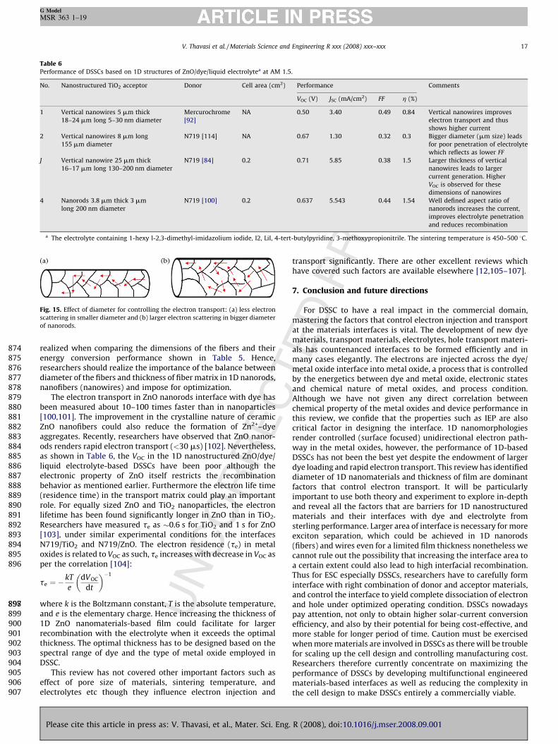
In one-dimensional (1D) nanostructures, the grain boundaeffect could be restricted (Fig. 15) [86,87]. Moreover, for the sa
g. R (2008), doi:10.1016/j.mser.2008.09.001
givenanoTiO2
thanobtaconsinvostruprepnano[89,tantan eSomwith
Ioxyg
718719720721722723724725726727728729730731732733734
TableA com
Nano
TiO2
TiO2
TiO2
TiO2
nan
ZnO
Dend
Fig. 1scatt
view
14
G Model
MSR 363 1–19
Ple
UN
CO
RR
EC
TED
PR
OO
Fn film thickness, the loading of dye can be much higher in 1Dstructured material than the nanoparticles, for instance, thenanowires has allowed for larger adsorption of dye, i.e. 4 timesthe P-25 [88]. The synthesis or preparation processes to
in 1D nanostructured material have been demanding but timeuming. 1D nanostructures could act as single crystal, andlve in rapid electron transport. The formation of crystallinecture should depend on the methodology that is used for thearation. The template assisted methodologies produce the 1Dstructured materials with polycrystallinity in structure
90], which limit the electron transport, whereas the surfac--controlled synthesis forms highly crystalline structure [89],ssential feature required for higher performance of DSSCs.e of the commonly used methodologies and their significanceregards to the application in DSSCs are pointed out in Table 3.
n 1D nanostructures, the surface is focused and hence, theen vacancy on the surface could be reduced and so act as
better n-type material with good electronic transport property.The recombination rate has been found to be 10 times slower in 1DTiO2 nanotubes which led for higher JSC (7.8 mA/cm2) than that ofnanoparticles (2.6 mA/cm2)-based DSSC [91]. Recently moreeffective charge transport has been realized when researchersattempted for direct deposition of rutile nanowires onto FTOconducting substrate [84]. However, the major problem of using1D nanostructured electrodes in DSSCs, is their poor adhesion tosubstrates that arises due to the high temperature used for thesintering. During sintering, strong stresses are generated that leadto the shrinkage of the fibrous mats. Such shrinkage has limited thebenefits of using 1D nanofibers film and resulting in poor chargecollection. Hence, direct attachment (binding) of 1D nanostruc-tured materials onto the conductive substrate (ITO or FTO) hasalways been challenging. Song et al. [92] have used thin film ofnanoparticles at the FTO as binding support for nanofibers on theFTO and also to prevent back electron transfer from ITO. Our group
3parison of current methodology used for 1D nanostructures.
structure Method Advantages Disadvantages
nanowires [80] Phase transformation of gel
matrix in shape container
Scattering of longer wavelength of light,
good electron transport
Slow process for wire growth
nanotubes aligned [81] Anodic oxidation of TiO2
thin film
Higher efficiency up to 2.9%, excellent
hollow structure
Low electrode thickness (360 nm),
small working area
nanotubes random [82] Surfactant assisted assemblies Higher photocurrent, larger electron transport, Slow process for nanotubes growth
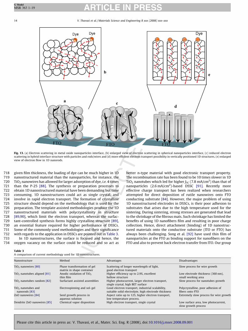
3. (a) Electron scattering in metal oxide nanoparticles interface, (b) enlarged view of electron scattering in spherical nanoparticles interface, (c) reduced electron
ering in hybrid interface structure with particles and rods/wires and (d) more efficient electron transport possibility in vertically positioned 1D structures, (e) enlarged
of electron flow in 1D nanorods.
V. Thavasi et al. / Materials Science and Engineering R xxx (2008) xxx–xxx
single crystal, high BET surface
nanotubes and
orods [83]
Electrospinning and sol–gel Good electron transport, industrial scalability,
suitable solid electrolyte, high electrode thickness
Polycrystalline, poor adhesion of
fibers onto FTO
nanowires [84] Seed growth process in
aqueous solution
Aspect ratio up to 125, higher electron transport,
low temperature process.
Extremely slow process for wire growth
rite ZnO nanowires [85] Chemical vapor disposition High electron transport, single crystal Low surface area, low photocurrent,
slow growth process
ase cite this article in press as: V. Thavasi, et al., Mater. Sci. Eng. R (2008), doi:10.1016/j.mser.2008.09.001

riditon
ivertrix1D
tro-thehaseenr FF
uldrgeallyore
g ofuseorenedicalvedthesedyettheser
andthe
ide/
752753754755756757758
759
760761762763764765766767768769770771772773774775776777778779780781782783784
s
t,
tion,
15
G Model
MSR 363 1–19
UN
CO
RR
EC
TED
PR
OO
Fhas recently successfully demonstrated direct deposition ofelectrospun TiO2 nanofibers by introducing an ultra-thin surfacetreatment layer (STL) on the FTO before depositing the TiO2
nanofibers. After calcination, the STL has behaved as an adhesivewhich retained adhesion of nanofibers on the conductive substrateand thus improved the adhesion of TiO2 nanofibers for betterelectron transport [93].
6.2. Effect of hybrid nanostructure
Hybrid nanostructures (Fig. 13c) have recently emerged as apromising architecture for electron transport as well as dyeadsorption. When the available quantity (and so the surface area)of spherical nanoparticles is larger in the hybrid structuredphotoanode film, especially towards the side that is disclosed forthe dye adsorption in comparison with the 1D nanostructuredmaterials, the maximum dye adsorption is possible on sphericalparticle surface, while the presence of nanofibers/rods, directs forfaster electron transport rate (Table 4).
For hybrid matrix, nanowires or rods that are used shouldpreferably have the same crystal structure as nanoparticles foreffective electron transport. Hybrid combination TiO2 nanowiresand P-25 with N719 dye has obtained an efficiency of 6.01% whichis about 60% higher than that of DSSC based on TiO2 nanowiresalone [94]. As seen in Table 4, the hybrid of different morphologicalcombination of TiO2 has increased FF significantly compared tothat of VOC. This indicates hybrid structure improves theinterpenetration of electrolyte in the hybrid matrix. The increaseof V of hybrid matrix of TiO has been found little when
than the other efficiency parameters, which suggests hybstructure increases the interfacial area that leads to more excdissociation and electron injection.
Although the 1D nanostructures have been proved to delhigher JSC than that of nanoparticles, the random aligned 1D macould be a barrier for the electrolyte interpenetration.nanostructure TiO2-based DSSCs with the standard liquid eleclyte have been found yielding relatively poor fill factor, i.e. is inrange of 0.5–0.8 for the efficient dyes such as N3 and N719. Thisraised the issue that the poor interpenetration is severe betw1D materials and the electrolyte. However, it is noted that lowehas been compensated by the higher JSC. Larger photocurrent coresult from the possibility of more excitons generation due to lainterface with dye and the controlled electron transport. Verticaligned 1D metal oxides (Fig. 13d) in DSSCs can promote mexciton generation because of the possibility of larger bindindye molecules. Furthermore, more dissociation can occur becaof the formation of larger interfacial area, followed by melectron injection and transport compared to the non-alig(random) 1D matrix. Matt Law et al. [95] have developed vertnanowires arrays of ZnO interface with N719 dye and obserthat vertical nanowires facilitates faster electron injection thanZnO nanoparticles/N719. However, the vertical nanowires-badevice even with efficient dyes such as N3 and N719 have notyielded the considerable performance (refer Table 5). One ofpossible reasons is the positioning of 1D nanomaterials. Clospacing of nanofibers/wires increases the exciton dissociationshould be preferred in order to obtain larger JSC. As known,efficiency parameter FF is influenced by the metal ox
Table 4Performance of hybrid materials/dye/liquid electrolytea in DSSC.
Nanostructured acceptor Donor Cell
area
(cm2)
Performance Values given in the bracket are the
one that has been obtained only by using the
material mentioned in ‘‘second combination’’ column
Comments
1D material Second
combination
VOC (V) JSC (mA/cm2) FF h (%)
TiO2 Nanorods
8.3 mm thick
10–20 nm diameter
TiO2P-25 N719 [90] NA 0.73 (0.704) 13.97 (12.74) 0.70 (0.649) 7.12 (5.82) Addition of nanorods
increases electrolyte
penetration, thus reduce
recombination, results in
larger JSC, VOC, and FF
TiO2P-25 TiO2 nanorods
15–18 mm
thick 150 nm
diameter
N3 [75] 1 0.834 (0.832) 13.3 (14.2) O.477 (0.366) 5.26 (4.28) Insertion of NP layer
slightly decreases curren
results in lower JSC
TiO2 nanowires
5.5 mm thick
5–30 nm diameter
TiO2P-25 N719 [88] 0.25 0.754 (0.714) 11.9 (8.16) 0.673 (0.710) 6.01 (4.13) Addition of nanowires
increases current genera
reduces recombination,
results in larger JSC, VOC
TiO2 nanowires
10–70 nm diameter
16 mm thick
TiO2P-25 N719 [91] NA 0.74 (0.74) 13.23 (12.11) 0.66 (0.63) 6.53 (5.59) Increase in thickness
increases the current
ZnO nanowires
5.5 mm thick
5–30 nm diameter
ZnONP Mercurochrome
[92]
NA 0.61 (0.49) 6.3 (3.4) 0.58 (0.50) 2.2 (0.84) Addition of
ZnO nanowires
significantly increases
current, electrolyte
penetration and so
reduces recombination,
results in larger JSC, VOC,
and FF
a The electrolyte containing 1-hexy l-2,3-dimethyl-imidazolium iodide, I2, LiI, 4-tert-butylpyridine, 3-methoxypropionitrile.
V. Thavasi et al. / Materials Science and Engineering R xxx (2008) xxx–xxx
eenthe(FF)ally
itss to
OC 2
compared to the single matrix (either P25 or nanofibers alone) andin some case, both are similar, suggesting the quasi Fermi energystate of the TiO2 is not affected by the hybrid composite. The hybridof ZnO nanofibers and nanoparticles with mercurochrome dye hasresulted with remarkable increase in the efficiency from 0.84% to2.2%. Over all, JSC of the hybrid composite has been found higher
Please cite this article in press as: V. Thavasi, et al., Mater. Sci. En
electrolyte interface. Better the interpenetrating network betwmetal oxide and electrolyte, larger the FF and thus, higherefficiency. Hence, the currently encountered poor fill factorissue in 1D architecture could also be improved in verticnanostructured materials provided if they are positioned withoptimal height and space between nanowires. Methodologie
g. R (2008), doi:10.1016/j.mser.2008.09.001

obtathemayit caprod
6.3.
Waspechandelivbasefar.TablandFF a1D nfor ethicbaseelecacco
L ¼
whete is
820821822823824
825
826827828829830831832833834835836837838839840
841842843
TablePerfoQ6
No.
1
2
3
4
5
6
7
8
a T
1 O
with
Fig. 1nano
16
G Model
MSR 363 1–19
Ple
UN
CO
RR
EC
TED
PR
OO
Fin such patterned nanostructures have been described well in
literatures [96,97]. Especially using electrospinning techniquebe promising to control precisely both spacing and position as
n be automated and moreover, has the potential for large scaleuction [98].1
Effect of nanodimensions
ith the advantages of having extremely high surface–volumect ratio and acting as a controlled unidirectional electronnel, the 1D nanostructures-based DSSC has been expected toer much higher conversion efficiency than the nanoparticles-d DSSC, however, it has not reached the best performance soComparing the performance of nanofibers-based DSSCs ine 4, it can be noted that the increase in the diameter of the fiberthickness of the fiber matrix has resulted in an increase in VOC,nd JSC. It can be realized that nanodimensions, i.e. diameter ofanostructured metal oxide and the thickness of matrix usedlectron transport play pivotal role. 1D nanostructures of larger
kness have been found to provide higher efficiency for TiO2-d DSSCs. It is to be noted that the diffusion coefficient oftron is a function of diffusion length and residence timerding to the correlation as follows:ffiffiffiffiffiffiffiffiffiffiffip
Increase in diffusion length speeds up electron transport innanoparticulate matrix by increasing the electronic mobility,simultaneously, it also increases the residence time of electron inthe matrix. The hybrid mixture of nanoparticulate matrix filmcould increase the diffusion length for the same given thickness ofnanoparticles matrix. For example, for the given film thickness of5.5 mm, the hybrid composite of ZnO-nanowires/nanoparticles asnanoparticles matrix enhances the De, i.e. 2.1 � 10�4 cm2 s�1 incomparison with the ZnO-nanoparticles alone as the matrix whoseDe is �7.2 � 10�5 [99]. Increasing the thickness beyond optimalpoint will lead for longer electron residence time in metal oxidematrix that endangers the DSSC performance by easing theelectron recombination with either the electrolyte or the reduceddye and also the energy state of metal oxide. High surface–volumeratio nature 1D nanostructure can accommodate more dyemolecules while maintaining the confined thickness in DSSCand hence, materials recombination could be restricted. Theelectrolyte ions surround the nanoparticles (Fig. 14), therebyneutralize the electrostatic field whereas 1D structures such asnanofibers/nanorods with larger diameter can realize its cylind-rical geometry that would create radial electric fields (Fig. 14),preventing the accumulation of more electrons, and therebyreducing chance for surface electron recombination.
It can be seen from Table 5 that nanorods morphology provides
5rmance of DSSCs based on 1D structures of TiO2/dye/liquid electrolytea at AM 1.5.
Nanostructured TiO2 acceptor Donor Cell
area
(cm2)
Performance Comments
VOC (V) JSC
(mA/cm2)
FF h (%)
Nanofibers 3.9 mm thick 20 nn diameter N3 [108] 1 0.826 9.88 0.51 4.14 Nanorods reduces recombination, reflects
as larger VOC and JSC
Nanofibers 20 mm thick 20 nm diameter N3 [109] 0.16 0.77 11.24 0.58 5.02 Larger thickness leads to larger current
Nanorods 15–18 mm thick 500–600 nm
long 150 nm diameter
N3 [75] 1.0 0.832 14.20 0.363 4.28 Longer length of nanorods increases the
larger dye adsorption and thereby current
to significantly larger (JSC)
Nanofibers 20 mm thick 20 nm diameter N3 [110] 0.16 0.77 8.67 0.60 4.01 Larger thickness leads to larger current generation
Nanowires 7.9 mm thick 20–50 nm diameter N719 [111] NA 0.74 2.70 0.67 1.30 Smaller thickness leads to lower current generation
Nanowires (20%) 10 mm thick 20 nm long
5–10 nm diameter
N719 [77] 0.25 0.72 19.22 0.67 9.33 Hybrid structures increases the current
and also electrolyte penetration
Nanofibers �7 � 3 mm thick 20 � 8 nm
diameter
N719 [112] NA 0.59 4.21 0.60 1.50 Smaller thickness leads to lower current generation
Nanorods 13.7 mm thick 100–300 nm
length 20–30 nm diameters
N719 [113] 0.25 0.767 13.10 0.728 7.29 Well defined aspect ratio of nanorods
increases the current, improves electrolyte
penetration and reduces recombination
he electrolyte containing 1-hexyl-2,3-dimethyl-imidazolium iodide, I2, LiI, 4-tert-butylpyridine, 3-methoxypropionitrile; the sintering temperature is 450–500 8C.
4. Pictorial view to show the effect of shape influences the electron transport: (a) severe space charge layer discernible on spherical nanoparticles, (b) radical effect of 1D-
fibers and (c) radical effect shown in the cross-sectional view of nanofibers.
V. Thavasi et al. / Materials Science and Engineering R xxx (2008) xxx–xxx
Dete; whereDe ¼ kTme=e; i:e:Late and Lame
re L is the diffusion length, De is electron diffusion coefficient,the residence time of electron and me is electron mobility.
ur group is currently focusing for controlled vertically patterned nanofibers
our industrial partners.
ase cite this article in press as: V. Thavasi, et al., Mater. Sci. En
larger JSC than that of nanofibers probably due to the well definedsize-shape aspect ratio. Reduction in the diameter of the 1Dnanostructures minimizes the grain interface effect as depicted inFig. 15a and b, hence may result in higher efficiency. Concurrently,nanofibers with too larger diameter should be conducive to widerand uncontrolled electron scattering (Fig. 15b). This effect can be
g. R (2008), doi:10.1016/j.mser.2008.09.001
ich7].
ain,ort
dyeeri-
inye/
lledatesion.eene inalsogiesth-sed
rgerfiedant
arlypthredomoreodswe
a toion.rm
ials,ronaysion
andised
874875876877878879880881882883884885886887888889890891892893894895896
897898899900901902903904905906907
ds
olyte
t,
ion
0 8C.
17
G Model
MSR 363 1–19
UN
CO
RR
EC
TED
PR
OO
Frealized when comparing the dimensions of the fibers and theirenergy conversion performance shown in Table 5. Hence,researchers should realize the importance of the balance betweendiameter of the fibers and thickness of fiber matrix in 1D nanorods,nanofibers (nanowires) and impose for optimization.
The electron transport in ZnO nanorods interface with dye hasbeen measured about 10–100 times faster than in nanoparticles[100,101]. The improvement in the crystalline nature of ceramicZnO nanofibers could also reduce the formation of Zn2+–dyeaggregates. Recently, researchers have observed that ZnO nanor-ods renders rapid electron transport (<30 ms) [102]. Nevertheless,as shown in Table 6, the VOC in the 1D nanostructured ZnO/dye/liquid electrolyte-based DSSCs have been poor although theelectronic property of ZnO itself restricts the recombinationbehavior as mentioned earlier. Furthermore the electron life time(residence time) in the transport matrix could play an importantrole. For equally sized ZnO and TiO2 nanoparticles, the electronlifetime has been found significantly longer in ZnO than in TiO2.Researchers have measured te as �0.6 s for TiO2 and 1 s for ZnO[103], under similar experimental conditions for the interfacesN719/TiO2 and N719/ZnO. The electron residence (te) in metaloxides is related to VOC as such, te increases with decrease in VOC asper the correlation [104]:
te ¼ �kT
e
dVOC
dt
� ��1
where k is the Boltzmann constant, T is the absolute temperature,and e is the elementary charge. Hence increasing the thickness of1D ZnO nanomaterials-based film could facilitate for largerrecombination with the electrolyte when it exceeds the optimal
transport significantly. There are other excellent reviews whhave covered such factors are available elsewhere [12,105–10
7. Conclusion and future directions
For DSSC to have a real impact in the commercial dommastering the factors that control electron injection and transpat the materials interfaces is vital. The development of newmaterials, transport materials, electrolytes, hole transport matals has countenanced interfaces to be formed efficiently andmany cases elegantly. The electrons are injected across the dmetal oxide interface into metal oxide, a process that is controby the energetics between dye and metal oxide, electronic stand chemical nature of metal oxides, and process conditAlthough we have not given any direct correlation betwchemical property of the metal oxides and device performancthis review, we confide that the properties such as IEP arecritical factor in designing the interface. 1D nanomorpholorender controlled (surface focused) unidirectional electron paway in the metal oxides, however, the performance of 1D-baDSSCs has not been the best yet despite the endowment of ladye loading and rapid electron transport. This review has identidiameter of 1D nanomaterials and thickness of film are dominfactors that control electron transport. It will be particulimportant to use both theory and experiment to explore in-deand reveal all the factors that are barriers for 1D nanostructumaterials and their interfaces with dye and electrolyte frsterling performance. Larger area of interface is necessary for mexciton separation, which could be achieved in 1D nanor(fibers) and wires even for a limited film thickness nonethelesscannot rule out the possibility that increasing the interface area certain extent could also lead to high interfacial recombinatThus for ESC especially DSSCs, researchers have to carefully fointerface with right combination of donor and acceptor materand control the interface to yield complete dissociation of electand hole under optimized operating condition. DSSCs nowadpay attention, not only to obtain higher solar-current conversefficiency, and also by their potential for being cost-effective,more stable for longer period of time. Caution must be exerc
Fig. 15. Effect of diameter for controlling the electron transport: (a) less electron
scattering in smaller diameter and (b) larger electron scattering in bigger diameter
of nanorods.
Table 6Performance of DSSCs based on 1D structures of ZnO/dye/liquid electrolytea at AM 1.5.
No. Nanostructured TiO2 acceptor Donor Cell area (cm2) Performance Comments
VOC (V) JSC (mA/cm2) FF h (%)
1 Vertical nanowires 5 mm thick
18–24 mm long 5–30 nm diameter
Mercurochrome
[92]
NA 0.50 3.40 0.49 0.84 Vertical nanowires improves
electron transport and thus
shows higher current
2 Vertical nanowires 8 mm long
155 mm diameter
N719 [114] NA 0.67 1.30 0.32 0.3 Bigger diameter (mm size) lea
for poor penetration of electr
which reflects as lower FF
J Vertical nanowire 25 mm thick
16–17 mm long 130–200 nm diameter
N719 [84] 0.2 0.71 5.85 0.38 1.5 Larger thickness of vertical
nanowires leads to larger
current generation. Higher
VOC is observed for these
dimensions of nanowires
4 Nanorods 3.8 mm thick 3 mm
long 200 nm diameter
N719 [100] 0.2 0.637 5.543 0.44 1.54 Well defined aspect ratio of
nanorods increases the curren
improves electrolyte penetrat
and reduces recombination
a The electrolyte containing 1-hexy l-2,3-dimethyl-imidazolium iodide, I2, LiI, 4-tert-butylpyridine, 3-methoxypropionitrile. The sintering temperature is 450–50
V. Thavasi et al. / Materials Science and Engineering R xxx (2008) xxx–xxx
bleost.thered
y in.
thickness. The optimal thickness has to be designed based on thespectral range of dye and the type of metal oxide employed inDSSC.
This review has not covered other important factors such aseffect of pore size of materials, sintering temperature, andelectrolytes etc though they influence electron injection and
Please cite this article in press as: V. Thavasi, et al., Mater. Sci. En
when more materials are involved in DSSCs as there will be troufor scaling up the cell design and controlling manufacturing cResearchers therefore currently concentrate on maximizingperformance of DSSCs by developing multifunctional engineematerials-based interfaces as well as reducing the complexitthe cell design to make DSSCs entirely a commercially viable
g. R (2008), doi:10.1016/j.mser.2008.09.001

Ack
VspecMedprovedgeman
Refe
[1]
[2][3]
[4][5][6][7][8][9]
[10][11]
[12][13]
[14][15]
[16]
[17]
[18]
[19][20][21]
[22]
[23]
[24]
[25][26]
[27]
[28]
[29][30]
[31]
[32]
[33]
[34][35]
[36][37][38]
[39][40]
[41]
[42]
[43]
[44]
951
952953954955956957
958
959960961962963964965966967968969970971972973974975976977978979980981982983984985986987988989990991992993994995996997998999
100010011002100310041005100610071008100910101011101210131014101510161017101810191020102110221023102410251026102710281029
18
G Model
MSR 363 1–19
Ple
UN
CO
RR
EC
TED
PR
OO
F
nowledgements
T and SR would like to express thanks to NUS President’s officeial program grant. VR also expresses his thanks to Harvardical School. Authors also acknowledge Mr. A. Kumar foriding his master degree thesis for reference. VT also acknowl-s to Dr. G. Balaji for his technical comments to improve thisuscript.
rences
M.A. Green, K. Emery, Y. Hisikawa, W. Warta, Prog. Photovoltaics 15 (2007)425–430.B. O’Regan, M. Graetzel, Nature 353 (1991) 737–740.Y. Kim, S. Cook, S.M. Tuladhar, S.A. Choulis, J. Nelson, J.R. Durrant, D.D.C. Bradley,M. Giles, I. McCulloch, C.-S. Ha, M. Ree, Nature Mater. 5 (2006) 197–203.W.U. Huynh, J.J. Dittmer, A.P. Alivisatos, Science 295 (2002) 2425–2427.N. Robertson, Angew. Chem. Int. Ed. 45 (2006) 2338–2345.H. Tian, F. Meng, Opt. Sci. Eng. 99 (2005) 313–329.M. Gratzel, Prog. Photovoltaics 14 (2006) 429–442.M.A. Green, Mater. Energy Convers. Dev. (2005) 3–34.S.E. Gledhill, B. Scott, B.A. Gregg, J. Mater. Res. 20 (2005) 3167–3179.M. Gorlov, L. Kloo, Dalton Trans. (2008) 2655–2666.O.V. Chervakov, M.V. Burmistr, O.S. Sverdlikovs’ka, V.H. Shapka, PolimerniiZhurnal 30 (2008) 5–13.H.J. Snaith, L. Schmidt-Mende, Adv. Mater. 19 (2007) 3187–3200.N. Kopidakis, K.D. Benkstein, J. Van de Lagemaat, A.J. Frank, J. Phys. Chem. B 107(2003) 11307–11315.J. Bisquert, Phys. Chem. Chem. Phys. 10 (2008) 3175–3194.J. Bisquert, A. Zaban, M. Greenshtein, I. Mora-Sero, J. Am. Chem. Soc. 126 (2004)13550–13559.A. Kambili, A.B. Walker, F.L. Qiu, A.C. Fisher, A.D. Savin, L.M. Peter, Physica E 14(2002) 203–209.N. Papageorgiou, M. Graetzel, P.P. Infelta, Sol. Energy Mater. Sol. Cells 44 (1996)405–438.A. Solbrand, H. Lindstroem, H. Rensmo, A. Hagfeldt, S.-E. Lindquist, S. Soedergren,J. Phys. Chem. B 101 (1997) 2514–2518.F. Cao, G. Oskam, P.C. Searson, J. Phys. Chem. 100 (1996) 17021–17027.T. Dittrich, Phys. Status Solidi A: Appl. Res. 182 (2000) 447–455.A. Solbrand, A. Henningsson, S. Soedergren, H. Lindstroem, A. Hagfeldt, S.-E.Lindquist, J. Phys. Chem. B 103 (1999) 1078–1083.M. Yanagida, K. Miyamoto, K. Sayama, K. Kasuga, M. Kurashige, Y. Abe, H.Sugihara, J. Phys. Chem. C 111 (2007) 201–209.A.N.M. Green, E. Palomares, S.A. Haque, J.M. Kroon, J.R. Durrant, J. Phys. Chem. B109 (2005) 12525–12533.H. Usui, H. Matsui, N. Tanabe, S. Yanagida, J. Photochem. Photobiol. A: Chem. 164(2004) 97–101.B.A. Gregg, M.C. Hanna, J. Appl. Phys. 93 (2003) 3605–3614.L. Hu, S. Dai, J. Weng, S. Xiao, Y. Sui, Y. Huang, S. Chen, F. Kong, X. Pan, L. Liang, K.Wang, J. Phys. Chem. B 111 (2007) 358–362.S.E. Shaheen, C.J. Brabec, N.S. Sariciftci, F. Padinger, T. Fromherz, J.C. Hummelen,Appl. Phys. Lett. 78 (2001) 841–843.C.J. Brabec, A. Cravino, D. Meissner, N.S. Sariciftci, T. Fromherz, M.T. Rispens, L.Sanchez, J.C. Hummelen, Adv. Funct. Mater. 11 (2001) 374–380.G.W. Crabtree, N.S. Lewis, Phys. Today 60 (2007) 37–42.M.K. Nazeeruddin, P. Pechy, T. Renouard, S.M. Zakeeruddin, R. Humphry-Baker,P. Comte, P. Liska, L. Cevey, E. Costa, V. Shklover, L. Spiccia, G.B. Deacon, C.A.Bignozzi, M. Graetzel, J. Am. Chem. Soc. 123 (2001) 1613–1624.M. Nilsing, P. Persson, S. Lunell, L. Ojamaee, J. Phys. Chem. C 111 (2007) 12116–12123.J. Rochford, D. Chu, A. Hagfeldt, E. Galoppini, J. Am. Chem. Soc. 129 (2007) 4655–4665.R. Jose, A. Kumar, V. Thavasi, K. Fujihara, S. Uchida, S. Ramakrishna, Appl. Phys.Lett. 93 (2008) 023125/023121–023125/023123.R. Jose, A. Kumar, V. Thavasi, S. Ramakrishna, Nanotechnology 19 (2008).E. Bae, W. Choi, J. Park, H.S. Shin, S.B. Kim, J.S. Lee, J. Phys. Chem. B 108 (2004)14093–14101.M. Nilsing, P. Persson, L. Ojamaee, Chem. Phys. Lett. 415 (2005) 375–380.H. Park, E. Bae, J.-J. Lee, J. Park, W. Choi, J. Phys. Chem. B 110 (2006) 8740–8749.A. Vittadini, A. Selloni, F.P. Rotzinger, M. Graetzel, J. Phys. Chem. B 104 (2000)1300–1306.K.S. Finnie, J.R. Bartlett, J.L. Woolfrey, Langmuir 14 (1998) 2744–2749.M.K. Nazeeruddin, R. Humphry-Baker, P. Liska, M. Graetzel, J. Phys. Chem. B 107(2003) 8981–8987.
[45] P. Wang, S.M. Zakeeruddin, P. Comte, R. Charvet, R. Humphry-Baker, M. Graetzel,J. Phys. Chem. B 107 (2003) 14336–14341.
[46] B. Wenger, M. Gratzel, E. Moser Jacques, J. Am. Chem. Soc. 127 (2005) 12150–12151.
[47] M. Graetzel, Inorg. Chem. 44 (2005) 6841–6851.[48] D.P. Hagberg, T. Marinado, K.M. Karlsson, K. Nonomura, P. Qin, G. Boschloo, T.
Brinck, A. Hagfeldt, L. Sun, J. Org. Chem. 72 (2007) 9550–9556.[49] J. Guo, D. Stockwell, X. Ai, C. She, N.A. Anderson, T. Lian, J. Phys. Chem. B 110
(2006) 5238–5244.[50] J. Guo, C. She, T. Lian, J. Phys. Chem. C 111 (2007) 8979–8987.[51] J.B. Asbury, E. Hao, Y. Wang, H.N. Ghosh, T. Lian, J. Phys. Chem. B 105 (2001)
4545–4557.[52] S. Iwai, K. Hara, S. Murata, R. Katoh, H. Sugihara, H. Arakawa, J. Chem. Phys. 113
(2000) 3366–3373.[53] C. Bauer, G. Boschloo, E. Mukhtar, A. Hagfeldt, Int. J. Photoenergy 4 (2002) 17–20.[54] G. Benko, P. Myllyperkio, J. Pan, P. Yartsev Arkady, V. Sundstrom, J. Am. Chem.
Soc. 125 (2003) 1118–1119.[55] W. Li, A.I. Frenkel, J.C. Woicik, C. Ni, S.I. Shah, Phys. Rev. B: Conden. Matter Mater.
Phys. 72 (2005) 155315/155311–155315/155316.[56] K. Keis, E. Magnusson, H. Lindstrom, S.-E. Lindquist, A. Hagfeldt, Sol. Energy
Mater. Sol. Cells 73 (2002) 51–58.[57] K. Kakiuchi, E. Hosono, S. Fujihara, J. Photochem. Photobiol. A: Chem. 179 (2006)
81–86.[58] X. Ai, N.A. Anderson, J. Guo, T. Lian, J. Phys. Chem. B 109 (2005) 7088–7094.[59] X. Ai, J. Guo, N.A. Anderson, T. Lian, J. Phys. Chem. B 108 (2004) 12795–12803.[60] H. Tributsch, Coord. Chem. Rev. 248 (2004) 1511–1530.[61] H. Tributsch, Appl. Phys. A: Mater. Sci. Process 73 (2001) 305–316.[62] H. Horiuchi, R. Katoh, K. Hara, M. Yanagida, S. Murata, H. Arakawa, M. Tachiya, J.
Phys. Chem. B 107 (2003) 2570–2574.[63] K. Keis, J. Lindgren, S.-E. Lindquist, A. Hagfeldt, Langmuir 16 (2000) 4688–4694.[64] N.A. Anderson, X. Ai, T. Lian, J. Phys. Chem. B 107 (2003) 14414–14421.[65] K. Hara, T. Horiguchi, T. Kinoshita, K. Sayama, H. Sugihara, H. Arakawa, Chem.
Lett. (2000) 316–317.[66] C.-Y. Chen, S.-J. Wu, C.-G. Wu, J.-G. Chen, K.-C. Ho, Angew. Chem. Int. Ed. 45
(2006) 5822–5825.[67] M.K. Nazeeruddin, P. Pechy, M. Graetzel, Chem. Commun. (1997) 1705–1706.[68] J.A. Pollard, D. Zhang, J.A. Downing, F.J. Knorr, J.L. McHale, J. Phys. Chem. A 109
(2005) 11443–11452.[69] D.F. Watson, G.J. Meyer, Coord. Chem. Rev. 248 (2004) 1391–1406.[70] Y. Diamant, S.G. Chen, O. Melamed, A. Zaban, J. Phys. Chem. B 107 (2003)
1977–1981.[71] P. Balaya, J. Jamnik, J. Fleig, J. Maier, J. Electrochem. Soc. 154 (2007) P69–
P76.[72] E. Kroeze Jessica, N. Hirata, S. Koops, K. Nazeeruddin Md, L. Schmidt-Mende, M.
Gratzel, R. Durrant James, J. Am. Chem. Soc. 128 (2006) 16376–16383.[73] A. Haque Saif, E. Palomares, M. Cho Byung, N.M. Green Alex, N. Hirata, R. Klug
David, R. Durrant James, J. Am. Chem. Soc. 127 (2005) 3456–3462.[74] A. Staniszewski, G.J. Meyer, PMSE Preprints 95 (2006) 294.[75] S.-J. Roh, R.S. Mane, S.-K. Min, W.-J. Lee, C.D. Lokhande, S.-H. Han, Appl. Phys. Lett.
89 (2006) 253512/253511–253512/253513.[76] E. Palomares, J.N. Clifford, S.A. Haque, T. Lutz, J.R. Durrant, J. Am. Chem. Soc. 125
(2003) 475–482.[77] Y.-J. Shin, J.-H. Lee, J.-H. Park, N.-G. Park, Chem. Lett. 36 (2007) 1506–1507.[78] C.M. Martin, V.M. Burlakov, H.E. Assender, Sol. Energy Mater. Sol. Cells 90 (2006)
900–915.[79] J.-A. He, R. Mosurkal, J. Kumar, L. Li, K.G. Chittibabu, L.A. Samuelson, Mater. Res.
Soc. Symp. Proc. 710 (2002) 213–218.[80] E. Palomares, A. Green, S.A. Haque, J.R. Durrant, Proc. SPIE-Int. Soc. Opt. Eng. 5520
(2004) 76–81.[81] F. Lenzmann, M. Nanu, O. Kijatkina, A. Belaidi, Thin Solid Films 451–452 (2004)
639–643.[82] S.A. Haque, E. Palomares, C. Xu, R.J. Potter, A.B. Holmes, J.R. Durrant, Proc. SPIE-
Int. Soc. Opt. Eng. 5215 (2004) 9–15.[83] F. Fabregat-Santiago, J. Garcia-Canadas, E. Palomares, J.N. Clifford, S.A. Haque,
J.R. Durrant, G. Garcia-Belmonte, J. Bisquert, J. Appl. Phys. 96 (2004) 6903–6907.
[84] T. Berger, T. Lana-Villarreal, D. Monllor-Satoca, R. Gomez, J. Phys. Chem. C 111(2007) 9936–9942.
[85] A.C. Bose, P. Balaya, P. Thangadurai, S. Ramasamy, J. Phys. Chem. Solids 64 (2003)659–663.
[86] K. Fujihara, A. Kumar, R. Jose, S. Ramakrishna, S. Uchida, Nanotechnology 18(2007) 365709/365701–365709/365705.
[87] J.B. Baxter, E.S. Aydil, Sol. Energy Mater. Sol. Cells 90 (2006) 607–622.[88] M. Adachi, Y. Murata, J. Takao, J. Jiu, M. Sakamoto, F. Wang, J. Am. Chem. Soc. 126
(2004) 14943–14949.[89] Y. Xia, P. Yang, Y. Sun, Y. Wu, B. Mayers, B. Gates, Y. Yin, F. Kim, H. Yan, Adv.
Mater. 15 (2003) 353–389.
V. Thavasi et al. / Materials Science and Engineering R xxx (2008) xxx–xxx
C. Bauer, G. Boschloo, E. Mukhtar, A. Hagfeldt, J. Phys. Chem. B 106 (2002) 12693–12704.K. Murakoshi, G. Kano, Y. Wada, S. Yanagida, H. Miyazaki, M. Matsumoto, S.Murasawa, J. Electroanal. Chem. 396 (1995) 27–34.V. Shklover, Y.E. Ovchinnikov, L.S. Braginsky, S.M. Zakeeruddin, M. Graetzel,Chem. Mater. 10 (1998) 2533–2541.A. Furube, M. Murai, S. Watanabe, K. Hara, R. Katoh, M. Tachiya, J. Photochem.Photobiol. A: Chem. 182 (2006) 273–279.
ase cite this article in press as: V. Thavasi, et al., Mater. Sci. En
[90] J.G. Lu, P. Chang, Z. Fan, Mater. Sci. Eng. R: Reports R52 (2006) 49–91.[91] K. Zhu, N.R. Neale, A. Miedaner, A.J. Frank, NanoLetters 7 (2007) 69–74.[92] M.Y. Song, Y.R. Ahn, S.M. Jo, D.Y. Kim, Mater. Res. Soc. Symp. Proc. 836 (2005)
107–112.[93] R. Zhu, C.-Y. Jiang, X.-Z. Liu, B. Liu, A. Kumar, S. Ramakrishna, Appl. Phys. Lett. 93
(2008) 013102/013101–013102/013103.[94] Y. Suzuki, S. Ngamsinlapasathian, R. Yoshida, S. Yoshikawa, Central Eur. J. Chem.
4 (2006) 476–488.
g. R (2008), doi:10.1016/j.mser.2008.09.001

Bull.
Phys.
007)
859–
11151116111711181119112011211122112311241125
19
G Model
MSR 363 1–19
UN
CO
RR
EC
TED
PR
OO
F
[95] M. Law, L.E. Greene, J.C. Johnson, R. Saykally, P. Yang, Nature Mater. 4 (2005)455–459.
[96] T. Kuykendall, P.J. Pauzauskie, Y. Zhang, J. Goldberger, D. Sirbuly, J. Denlinger, P.Yang, Nature Mater. 3 (2004) 524–528.
[97] G.T. Wang, A.A. Talin, D.J. Werder, J.R. Creighton, E. Lai, R.J. Anderson, I. Arslan,Nanotechnology 17 (2006) 5773–5780.
[98] V. Thavasi, G. Singh, S. Ramakrishna, Energy Environ. Sci. 1 (2008), doi:10.1039/b809074m.
[99] C.-H. Ku, J.-J. Wu, Appl. Phys. Lett. 91 (2007) 093117/093111–093117/093113.[100] A.B.F. Martinson, J.E. McGarrah, M.O.K. Parpia, J.T. Hupp, Phys. Chem. Chem.
Phys. 8 (2006) 4655–4659.
[101] K.S. Kim, Y.-S. Kang, J.-H. Lee, Y.-J. Shin, N.-G. Park, K.S. Ryu, S.H. Chang,Korean Chem. Soc. 27 (2006) 295–298.
[102] E. Galoppini, J. Rochford, H. Chen, G. Saraf, Y. Lu, A. Hagfeldt, G. Boschloo, J.Chem. B 110 (2006) 16159–16161.
[103] M. Quintana, T. Edvinsson, A. Hagfeldt, G. Boschloo, J. Phys. Chem. C 111 (21035–1041.
[104] A. Zaban, M. Greenshtein, J. Bisquert, Chem. Phys. Chem. 4 (2003)864.
[105] S. Fujihara, K. Kakiuchi, E. Hosono, Electrochemistry (2005) 133–157.[106] A. Zaban, Nanocryst. Metals Oxides (2002) 209–234.[107] C. Longo, M.-A. De Paoli, J. Braz. Chem. Soc. 14 (2003) 889–901.
V. Thavasi et al. / Materials Science and Engineering R xxx (2008) xxx–xxx
Please cite this article in press as: V. Thavasi, et al., Mater. Sci. Eng. R (2008), doi:10.1016/j.mser.2008.09.001