matt bellismaterias.fi.uba.ar/6644/info/generadores/basico/course - source... · matt bellis...
TRANSCRIPT

Matt Bellis
Hewlett-Packard Company
Microwave Instruments Division
1400 Fountaingrove Parkway
Santa Rosa, California 95403
U.S.A.
1997 Back to Basics Seminar
����������
This literature was published years prior to the establishment of Agilent Technologies as a company independent from Hewlett-Packard and describes products or services now available through Agilent. It may also refer to products/services no longer supported by Agilent.We regret any inconvenience caused by obsolete information. For the latest information on Agilent’s test and measurement products go to:
www.agilent.com/find/products
Or in the US, call Agilent Technologies at 1-800-452-4844 (8am–8pm EST)

Abstract
To prepare you for the challenges of today's signalgeneration, we'll cover the basics on the signals required totest a variety of products from amplifiers to highly securecommunication systems. These signals may be as simpleas a single frequency sinusoid or as complex as a digitallymodulated carrier. This seminar reviews the basics ofsignal generators and the applications where signalgenerators are used. Block diagrams will be reviewedwhere appropriate. Signal generator specifications willalso be discussed.
Author
Mr. Bellis holds a BSEE and BA in Physics fromNorthwestern University. He holds an MSEE from theUniversity of California at Santa Barbara. During his careerhe has worked in both R&D and Marketing. Mr. Bellisworked at Northrop Corporation on the B2 program. AtNorthrop, he studied the interaction of materials withelectromagnetic waves with applications incommunications, signature suppression, and electronicwarfare. Currently he is with the Microwave InstrumentDivision of Hewlett-Packard where he is responsible forunderstanding the test needs of the wirelesscommunications industry.
H

Slide #1
A signal source produces sine waves. This is the most basic definition of a signal source.
In this seminar, three types of sources will be reviewed. Block diagrams will be used to explain how sourceswork. For each type of source, several applications will be reviewed and the critical specifications for eachapplication will be emphasized.
H
Agenda
Types of sources
CW
Swept
Signal Generator
Specifications
Block Diagrams
Applications
2 - 1
HSource Basics

Slide #2
Sources generate sine waves. Sine waves are used in many, many test and measurement applications. The idealoutput is shown in both the time domain and the frequency domain. The time domain waveform is expressed by:
v(t) = vosin(2pfot)
Using Fourier analysis, the time domain waveform may be transformed to a frequency domain representation:
V(f) = ∫−∞+∞
v(t)e−j2πftdt
= ∫−∞+∞
vosin(2πfot)e−j2πftdt
= -jvo/2[d(f - fo) - d(f + fo)]
Where the function d( ) is the impulse function. The Fourier transform is a two-sided representation withimpulse functions centered at both fo and -fo. The amplitude of each impulse function is vo/2. The equivalentsingle sided representation is a single impulse function at fo with an amplitude of vo.
The performance specifications for sources identify the range of output power and frequencies available. Inaddition, specifications identify deviations from the ideal sine wave. These deviations can be intentional, such asadding modulation capabilities, or unintentional.
H
Sources Generate Sine Waves
Voltage
Time
Voltage
Frequency
This is the ideal output: most specs deal with deviations from
the ideal and adding modulation to a sine wave
RF Microwave Millimeter
20-30 GHz 300 GHz3-6 GHz
Spectrum AnalyzerOscilloscope
2 - 2
HSource Basics

Slide #3
Three basic types of sources will be discussed: CW sources, swept sources, and signal generators. A source thatproduces a single sine wave is referred to as a CW source. The frequency and the amplitude of the sine wave canbe set to a desired value in most CW sources. A swept source adds the ability to automatically vary the outputfrequency or amplitude of a sine wave over a range of frequencies or amplitudes. Some swept sources have theability to vary frequency and amplitude simultaneously. When modulation is added to a sine wave, the source is asignal generator. Signal generators output "signals" : Sine waves that carry information. There are numerousmethods for adding information to a sine wave. Basics signal generators have amplitude, frequency, and phasemodulation capabilities. More advanced signal generators have pulse and IQ modulation capabilities.
H
CW
generates a single frequency, fixed sine wave
Swept
sweeps over a range of frequencies
may be phase continuous
Signal Generator
adds modulation
produces "real world" signal
Types of Sources
2 - 3
HSource Basics

Slide #4
H
Agenda
Types of sources
CW
Swept
Signal Generator
Summary
2 - 4
HSource Basics

Slide #5
Understanding source specifications is critical when determining the appropriate source for an application. ForCW sources, the specifications are generally divided into three broad categories: Frequency, amplitude (oroutput), and spectral purity.
Range, resolution, and accuracy are the main frequency specifications. Range specifies the range of outputfrequencies that the source can produce. Resolution is the smallest frequency increment. The accuracy of asource is affected by two parameters: The stability of the reference oscillator and the amount of time that haspassed since the source was last calibrated. A typical (but very good) reference oscillator may have an aging rateof 0.152ppm (parts-per-million) per year. The aging rate indicates how far the reference will drift (either up ordown) from its specified value. At 1 GHz, a source that has not been calibrated for one year with an aging rate of0.152ppm per year will be within 152 Hz of its specified output frequency.
H
CW Source Specifications...Frequency
.
Voltage
Frequency
Uncertainty
Range: Range of frequencies covered by the source
Resolution: Smallest frequency increment
Accuracy: How accurately can the source frequency be set
Switching Speed: Automated test applications
EXAMPLE
Accuracy =
= CW frequency = 1 GHz
= aging rate = 0.152ppm/year
= time since last calibrated = 1 year
+_ fCW τaging calτ* *
fCW
τaging
calτ
Accuracy = 152 Hz+_
2 - 5
HSource Basics

Slide #6
Range, accuracy, resolution, switching speed, and reverse power protection are the main amplitudespecifications. The range of a source is determined by the maximum output power and the amount of internalattenuation built into the source. Sources monitor their own output power to maintain amplitude accuracy.Automatic leveling circuits are used to measure the output. The resolution of a source indicates the smallestamplitude increment. Switching speed is a measure of how fast the source can change from one amplitude levelto another.
Sources are often used to test transceivers. Because transceivers have transmitters, the connection between asource and the transceiver could conduct a signal from the device being tested to the output connector of thesource. Reverse power protection prevents signals traveling the wrong direction from damaging the source.
H
CW Source Specifications...Amplitude
DUT
Source protected from accidental transmission
fromDUT
Voltage
Frequency
How accurate isthis number?
What is P out?
What is P out?max
min
Range (-136dBm to +13dBm)
Accuracy (+/- 0.5dB)
Resolution (0.02dB)
Switching Speed (25ms)
Reverse Power Protection
2 - 6
HSource Basics

Slide #7
The specifications associated with spectral purity are often the most difficult to understand. The ideal CW outputis a sine wave at a single frequency. Unfortunately, their are no ideal CW sources: All sources are made withnon-ideal (i.e. real) components. These components introduce phase noise and unwanted distortion products.
Harmonic spurs are integer multiples of the CW output. Sources contain many non-linear components. Thesecomponents are needed to provide a broad range of frequencies and output powers. Consider the output of anamplifier:
vo(t) = a1 vi(t) + a2 vi2(t) + a3 vi
3(t) + ...
For an input sine wave, the output is:
vo(t) = a1 sin(wt) + a2 sin2(wt) + a3 sin3(wt) + ...
= a2/2 + a1 sin(wt) + 3a3/4 sin(wt)+ a2/2 sin(2wt) + a3/4 sin(3wt) +...
The non-linear characteristics of an amplifier create second, third, and higher order harmonics. A typical secondharmonic will be specified at <-30 dBc (better than 30 dB below the output of the fundamental frequency).Non-harmonic spurs come from a variety of sources (e.g. power supply) and are typically quite low (<-65 dBc).
Multipliers are often used in sources to extend the frequency output. This results in the presence ofsub-harmonics.
H
Phase Noise
Residual FM
Spurious
CW Source Specifications...Spectral Purity
non-harmonic spur
~65dBc
harmonic spur
~30dBc
CW output
residual FM is
the
integrated
phase noise
over 300 Hz -
3 kHz BW
phase
noise
0.5f0 f0 2f0
sub-harmonics
2 - 7
HSource Basics

Slide #8
In the ideal case, all of the power in a sine wave is concentrated at a single frequency. Random noise within thesource will cause the power to be spread over a small range of frequencies. The spread is referred to as phasenoise and is often mathematically modeled as random phase modulation. The units of phase noise are dBc/Hz:dB down from the carrier in a 1 Hz bandwidth. Phase noise is specified at a frequency offset from the CW output.For example, the phase noise of a CW source may be specified as: -97dBc/Hz @ 100 kHz offset from a CWfrequency at 20 GHz.
Phase noise may be directly measured from the spectrum of a source. This method requires that the phase noiseof the analyzer be much better (~10dB) than the phase noise of the source being tested. Often, the phase noise ofa source is measured using test equipment that has been optimized for this purpose. Phase noise is generallydisplayed on a log-log axis. This enables both the close in phase noise (offsets < 1 kHz) and the far out phasenoise (offsets > 10 kHz) to be easily examined on one plot.
The phase noise plot above was generated using the HP 89441A by displaying the power spectral density (units ofdBm/Hz) of a phase demodulated signal. The source is at 1 GHz. The marker is at a 10 kHz offset and reads-104dBc/Hz.
Residual FM is a measure of the small amount of FM inherent in an CW output. Residual FM is specificied withina bandwidth. Most sources typically specify residual FM per the CCITT specified bandwidth. The CCITTbandwidth starts at 300 Hz offset from the carrier frequency and stops at a 3 kHz offset. Within this band, all ofthe noise shown on the phase noise curve contributes to residual FM. ..
H
CW Source Specifications... Spectral Purity: Phase Noise
CWoutput
frequency
PowerSpectralDensity
measured as dBc/Hz
Ch1 PMPSD
-104.177 dB*
1k 10k 100k
TRACEA:
AMarker 10 000 Hz
Start: 500 Hz Stop: 100 kHz
Y* = radrms^2/Hz-75
dB*
-125
dB*
LogMag
5dB
/div
2 - 8
HSource Basics

Slide #9
The block diagram of a CW source can be divided into three major sections: Reference, synthesizer, and output.Each section has a unique role in producing a sine wave and makes a unique contribution to the sourcespecifications.
H
CW Block Diagram
Output Section
range
level accuracy
amplitude switching speed
reverse power protection
Reference Section
frequency stability
accuracy
Synthesizer Section
range
resolution
switching speed
spectral purity
2 - 9
HSource Basics

Slide #10
The above block diagram provides greater detail for an RF CW source.
The reference section supplies the reference oscillator for the source. The reference oscillator contributes to theshort term stability of the output frequency (phase noise). The long term stability of the reference oscillator, theaging rate, determines the accuracy of the output frequency.
The reference section supplies a sine wave with a known frequency to the synthesizer section. This sine wave isused as the reference for a phase-locked loop (PLL). The synthesizer section is responsible for producing a cleansine wave at the desired frequency. The VCO (voltage controlled oscillator) produces the sine wave. The PLLmaintains the output frequency at the desired setting and translates the frequency accuracy of the referenceoscillator to the output of the VCO.
The synthesizer section supplies a clean sine wave to the output section. The output section determines theoverall amplitude range and accuracy of the source. Amplitude range is determined by the available amplificationand attenuation. Amplitude accuracy, or level accuracy, is maintained by monitoring the output power andadjusting the power as needed.
Let's take a look at each section in more detail.
H
RF CW Block Diagram
Reference
Oscillator
VCO
Phase
Detector
Frac-N
divide
by X
ALC
Modulator
ALC
Driver
ALCDetector
Output
Attenuator
ALC= automatic level control
Reference Section
Synthesizer Section
Output Section
2 - 10
HSource Basics

Slide #11
The heart of the reference section is the reference oscillator. The reference oscillator must be inexpensive,extremely stable and adjustable over a narrow range of frequencies. A stable reference oscillator will ensure thatthe frequency output of the source remains accurate in between calibrations. By comparing the referenceoscillator to a frequency standard, such as a Cesium oscillator, and adjusting as needed, the source can becalibrated with an output that is traceable.
Of all materials today, crystalline quartz best meets these criteria. The fundamental frequency of quartz isaffected by several parameters: aging, temperature, and line voltage. Over time, the stress placed on a quartzcrystal will affect the oscillation frequency. Temperature changes cause changes in the crystal structure whichaffect the oscillation frequency. The piezoelectric nature of quartz is also affected by the electric fields createdinside the source by the line voltage.
To improve the performance of quartz, temperature compensation circuitry is used to limit the variations inoutput frequency that result from variations in the operating temperature. Crystals with such compensation arereferred to as Temeprature Compensated crystal oscillators or TCXO's. OCXO's are crystals that have beenplaced in an Oven Controlled environment. This environment maintains a constant temperature and providesshielding from the affects of line voltage. The stability for both TCXO's and OCXO's is tabulated above.
Many sources provide an external input that may be used to lock the oscillator to an external reference. Thesource, however, does not require an external reference.
H
RF CW Block DiagramReference Section
Phase
Detector
Optional External
Reference Input Reference Oscillator (TCXOor OCXO)
TCXO OCXO
Aging Rate +/- 2ppm/year +/- 0.1 ppm /year
Temperature +/- 1ppm/year +/- 0.01 ppm/year
Line Voltage +/- 0.5ppm/year +/- 0.001 ppm/year
to synthesizer section
divide
by X
2 - 11
HSource Basics
Slide #12
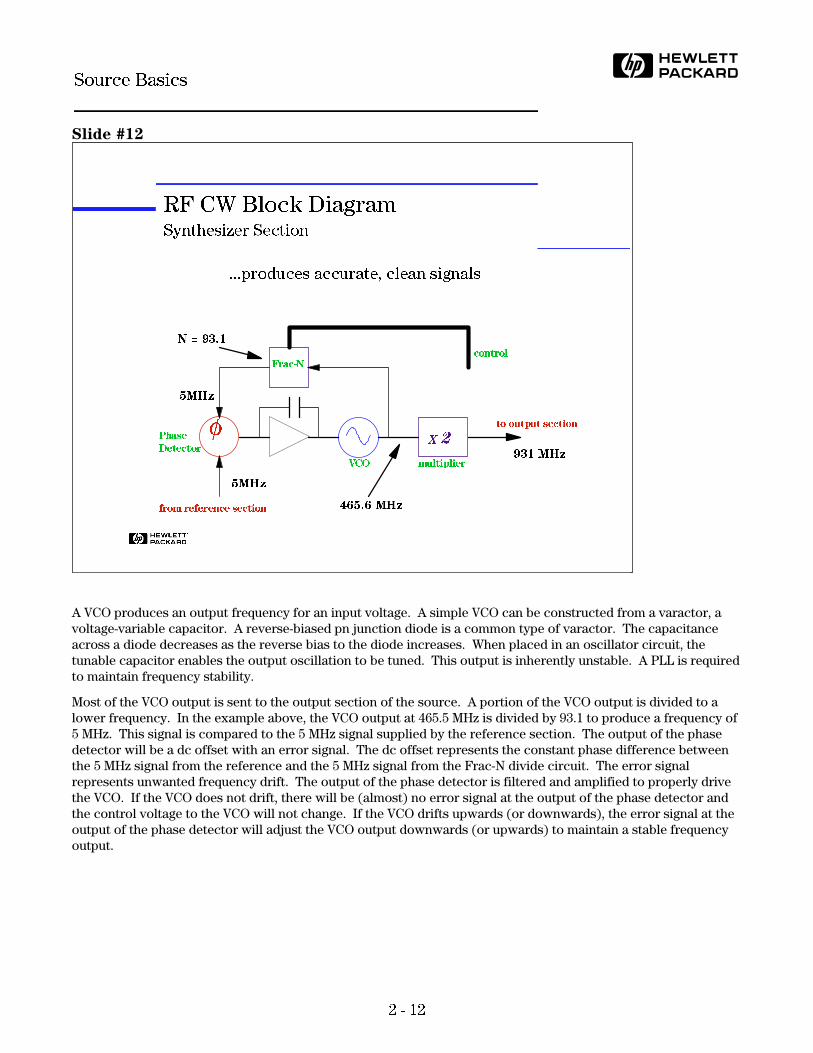
A VCO produces an output frequency for an input voltage. A simple VCO can be constructed from a varactor, avoltage-variable capacitor. A reverse-biased pn junction diode is a common type of varactor. The capacitanceacross a diode decreases as the reverse bias to the diode increases. When placed in an oscillator circuit, thetunable capacitor enables the output oscillation to be tuned. This output is inherently unstable. A PLL is requiredto maintain frequency stability.
Most of the VCO output is sent to the output section of the source. A portion of the VCO output is divided to alower frequency. In the example above, the VCO output at 465.5 MHz is divided by 93.1 to produce a frequency of5 MHz. This signal is compared to the 5 MHz signal supplied by the reference section. The output of the phasedetector will be a dc offset with an error signal. The dc offset represents the constant phase difference betweenthe 5 MHz signal from the reference and the 5 MHz signal from the Frac-N divide circuit. The error signalrepresents unwanted frequency drift. The output of the phase detector is filtered and amplified to properly drivethe VCO. If the VCO does not drift, there will be (almost) no error signal at the output of the phase detector andthe control voltage to the VCO will not change. If the VCO drifts upwards (or downwards), the error signal at theoutput of the phase detector will adjust the VCO output downwards (or upwards) to maintain a stable frequencyoutput.
H
RF CW Block DiagramSynthesizer Section
VCO
Phase
Detector
Frac-N
from reference section
to output section
X 2
multiplier
control
5MHz
465.6 MHz
N = 93.1
931 MHz
5MHz
...produces accurate, clean signals
2 - 12
HSource Basics

Slide #13
The synthesizer section of a source has a tremendous impact on the overall phase noise of the source. There arefour main contributors to phase noise: The reference oscillator, the phase detector, the VCO, and the broadbandnoise floor. The broadband noise floor results primarily from the thermal noise present in the source. In general,this noise does not greatly limit the performance of the source. The phase noise of the reference oscillator andthe VCO both fall off initially as 1/f3 and transitions to a 1/f2 dependence. On a log-log plot, 1/f2 translates to aslope of 20 dB per decade. The phase noise contribution of the phase detector is dominated by thermal noise andhence exhibits the same spectral dependency (or lack of spectral dependency) as the broadband noise floor. Inaddition, the Frac-N divide in the PLL degrades the phase noise performance by 20logN where N is the divide bynumber.
The bandwidth of the PLL determines the point at which the VCO contribution to the overall phase noise becomessupressed. For frequency offsets inside the PLL bandwidth, the overal phase noise of the source is dependentmainly upon contributions from the phase detector and the reference oscillator.
.
H
RF CW Block Diagram
Synthesizer Section
reference
oscillator
phase noise of source
VCO noise
phase
detector
noisebroadband
noise floor
20logN
phase-locked-loop (PLL)
bandwidth selected for
optimum noise performance
PLL / Fractional - N
...suppresses phase noise
frequency
noise
2 - 13
HSource Basics

Slide #14
The output section maintains amplitude or level accuracy by measuring the output power and compensating fordeviations from the set power level. The ALC driver digitizes the detector output and compares the digitizedsignal to a look-up table. The appropriate modulator drive is generated such that the detected power becomesequivalent to the desired power. Frequently, external losses from cabling and switching between the output ofthe signal source and the device under test (DUT) attenuate the signal. A look-up table that compensates forexternal losses can be input to extend the automatic leveling to the input of the DUT.
With no output attenuation applied, the source amplitude is at a maximum. The maximum amplitude isdetermined by the power amp and the loss between the output of the amp and the output connector. The mainsource of loss is the output attenuator. The output attenuator will introduce a finite amount of loss even when theattenuation is set to 0 dB. The purpose of the output attenuator is to reduce the output power in a calibrated andrepeatable fashion. Today attenuators are available that provide output ranges from +13 dBm (no attenuationapplied to the source) to -136 dBm (maximum attenuation applied). There are two types of attenuators that arecommonly used: mechanical and solid state.
Mechanical attenuators introduce very little loss between the output of the power amp and the output connector.Thus a high output power can be achieved without over-driving the output amplifier. Operating at low drive levelsreduces the level of harmonics generated by the source. Mechanical attenuators do, however, have finitelifetimes. A typical mechanical attenuator will live for five million cycles. For an ATE application in which thepower level is changed every two seconds, the attenuator will fail after about a year.
Solid state or electronic attenuators have essentially infinite lifetimes. For ATE applications, solid stateattenuators are well suited. Solid state attenuators do introduce significant loss even when no attenuation isdesired. Higher output amplifier drive levels are required in sources with solid state attenuators to overcome thelosses. The higher drive levels increase the level of the harmonics. Sources with solid state attenuators,therefore, require more sophisticated designs to maintain an equivalent level of spectral purity with sources thatuse mechanical attenuators.
H
RF CW Block DiagramOutput Section
ALC = automatic level control
ALC
Modulator
ALC
Driver
ALC Detector
Output
Attenuatorfrom
synthesizer
section source output
ALC
maintains output
power by
adding/subtracting
power as needed
Output Attenuatormechanical or
electronic
provides attentuation
to achieve wide output
range (e.g. -136dBm to
+13dBm)
2 - 14
HSource Basics

Slide #15
The block diagram of a microwave CW source is similar to that of an RF CW source; each has the same threebasic sections. There are differences, however. Although the reference section only has one reference oscillator,two signals are supplied to the synthesizer section from the reference section. The output frequency of thesynthesizer section is generated from a Yttrium-iron-garnet (YIG) oscillator which is tuned with a magnetic field.The feedback mechanism that ensures frequency stability is a phase locked loop; however, instead of afractional-N divide, harmonic sampling is used to divide the output frequency.
Again, we will take a look at these sections in detail.
H
µWave CW Block Diagram
ALCDetector
ALC
Modulator
ALC
Driver
Output
Attenuator
Sampler
Reference Section
Synthesizer
SectionOutput Section
Ref Osc
VCO
Phase
Det
Frac
N
by X
VCO
Phase
Detector
Frac-N
Phase
DetectorTuning
Coils
YIG
Oscillator
2 - 15
HSource Basics

Slide #16
The reference oscillator for a microwave source is either a quartz TCXO or OCXO. As with RF sources, thereference oscillator is inside a PLL that may be locked to an external reference. In addition, the referenceoscillator drives a PLL that contains an RF VCO. For some microwave sources, this VCO will produce an outputfrequency in the 300 - 350 MHz range. This higher frequency reference is needed by the harmonic sampler in thesynthesizer section.
H
µWave CW Block DiagramReference Section
Reference
Oscillator
VCO
Phase
Detector
Frac-N
multiply
by X
10 MHz
x3
30 MHz
300 - 350 MHz
to synthesizer section
Ext Ref
2 - 16
HSource Basics

Slide #17
The heart of the synthesizer section is a YIG oscillator. YIG oscillators (YO's) have extremely wide tuning rangesand low phase noise. They are ferromagnetic and are tuned with an electromagnetic tuning coil. In the absenceof feedback, YO's do not exhibit good frequency stability.
To achieve good frequency stability, the YO is placed inside a PLL. A portion of the YO's output is sent to thesampler. The reference section supplies the sampler LO. A pulse forming circuit inside the sampler generatesharmonics of the LO. Each harmonic mixes with the output of the YO. The IF output of the sampler is filtered.The resulting signal is the YO frequency subtracted from the closest harmonic of the LO. For example, supposethe YO frequency is 9.01 GHz, the sampler LO is 310 MHz, and the IF filter passes signals from 18 MHz to 26 MHz.The YO frequency will mix with the 29th harmonic of the LO, 8.99 GHz, to produce a 20 MHz IF. The 28thharmonic, at 8.68 GHz, will produce an IF output of 330 MHz which will be removed by the bandpass filter.Similarly, the 30th harmonic, at 9.3 GHz, will produce an IF output of 290 MHz which will also be removed.
The reference for the YO PLL is supplied by a VCO. The VCO is stabilized in a separate PLL whose reference issupplied by the reference section.
The output of the phase detector in the YO PLL is used to drive the tuning coils of the YO. This locks the YO to aninteger multiple of the sampler LO minus a fixed integer ratio of the YO PLL reference. This technique enablesmicrowave sources to achieve extremely good frequency resolution.
H
µWave CW Block DiagramSynthesizer Section
VCO
Phase
Detector
Frac
N
from reference section
Sampler
Phase
DetectorTuning
Coils YIG
Oscillator
9.01 GHz
divide
by x
divide
by y
from reference section
n = 29 then f =8.99GHz
and f =20MHz
LO
IF
IF
2 - 17
HSource Basics

Slide #18
The pulse forming circuit inside the sampler creates a frequency comb. This comb contains the sampler LO andall of its harmonics. The comb enables the YO output to be mixed down to a lower frequency. In place of asampler, a series of fixed oscillators could be used to mix the YO output down to a level where a fractional-Ndivide could be used. This adds cost and hardware complexity to the source. Using a sampler does requiresophisticated firmware algorithms, however, the cost and complexity of the hardware is reduced.
H
µWave CW Block DiagramSynthesizer Section
frequency
310 MHz
n = 1 2 3 4 5 27 28 29 30 31
8.99 GHz
Sampler mixes one of the
harmonics with the output
of the YIG oscillator
Comb Generator
2 - 18
HSource Basics

Slide #19
There are many, many applications for RF and microwave CW sources. The list above represents only a portionof the more common applications.
H
Applications & Critical Specifications
Local Oscillator
phase noise
frequency accuracy
Amplifier Distortion
spurious
TOI (for system)
Receiver Testing
Spurious
spurious
level accuracy
2 - 19
HSource Basics

Slide #20
CW sources are often used as local oscillators in the development of transmitters and receivers.
Frequently during development, hardware sections of a prototype become available in stages. CW sources areoften used in place of unfinished sections. For example, in the development of transmitter, if all sections exceptthe local oscillator section are finished, a CW source is often used as the local oscillator.
When using a CW source as a local oscillator, phase noise and frequency accuracy are critical. Poor frequencyaccuracy will, for example, cause a transmitter to transmit at the wrong frequency. In a channelizedcommunication system, poor phase noise will spread energy into adjacent channels. This spread into adjacentchannels could be incorrectly attributed to the power amps of a transmitter.
H
Applications & Critical SpecificationsAs a Local Oscillator
IF signal transmitter output
poor phase noise spreads
energy into adjacent
channelspoor frequency
accuracy will cause
transmitter to be at
the wrong frequency
DUT
2 - 20
HSource Basics

Slide #21
Third order intercept, or TOI, is a common amplifier measurement. In this measurement, two CW sources arecombined at the input of an amplifier. The frequencies of each source are slightly offset from each other and yetstill inside the bandwidth of the amplifier. The non-linearities of an amplifier will produce third order mixingproducts:
fL = 2f1 - f2
fU = 2f2 - f1
where f1 and f2 are the output frequencies of the two sources.
Spurious signals from the CW sources can corrupt the measurement. When selecting an appropriate source, thenon-harmonic spurious levels should be well below the third order products produced by the amplifier under test.
The test system can also introduce sources of error. Whenever two signals are input to a combiner, thenon-linearities of the sources will create intermodulation products. The intermodulation products, when using asimple combiner, are created by the ALC of the source. The signal from the first source passes through theresistive combiner network and into the second source output with a 6 dB loss and the loss associated with theoutput attenuation of the second source. Because the two sources are at different frequencies, the sum of the twosignals has an AM component equal to the difference frequency. For difference frequencies that are within thebandwidth of the ALC, the ALC of the second source sees this additional power and tries to level the output byadding AM. The intermodulation products created by the test system are at the same frequencies as those createdby the amplifier under test.
Intermodulation products can be reduced either through better isolation of the signal sources or by suppressingthe power that transfers from one source to the other.
H
Applications & Critical Specifications
Amplifier Testing
f2f1
fU = 2f2 -f1fL = 2f1 -
f2
spurious signals from
source can corrupt
measurement
frequency
am
plitude
test system third order
products will also fall
here
output RF
isolator
f1
f2
DUTIntermodulation
Distortion
2 - 21
HSource Basics

Slide #22
Spurious immunity is a measure of the ability of a receiver to prevent unwanted signals from causing an unwantedresponse at the output of the receiver. To make this measurement, one source inputs a modulated test signal atthe desired channel frequency at a level above the sensitivity of the receiver. The second source outputs aninterfering signal over a broad range of frequencies. The interfering signal may be modulated or unmodulateddepending upon the frequency range and the communication standard. The output amplitude of the interferingsignal is adjusted until the BER (for digital systems) or SINAD (for analog systems) of the receiver under test isdegraded to a specified level. The difference between the test signal and the interfering signal is the spuriousimmunity of the receiver:
aspur = Pinterferer - Ptest
The non-harmonic spurious output of the interfering source must be at sufficiently low levels to ensure that themeasurement is not affected. The non-harmonic spurious signals should be about 15 dB below the spuriousimmunity specification. At this level, spurs from the source will make only a minimal contribution to the overallin-channel noise floor.
The level accuracy also affects the test. An example will illustrate how. If the set level of the interferer is 0dBmand the set level of the test signal is -50dBm then the spurious immunity is 50dB. If the level accuracy of the twosources is +/-1dB, then the level of the interferer might actually be -1dBm and the level of the test signal mightactually be -49dBm. This results in an actual spurious immunity of 48dB; not quite as good. By considering thelevel accuracy of the sources, an uncertainty for the measurement can be determined. In this case, the measuredspurious immunity is 50dB +/- 2dB. The uncertainty is twice the level accuracy.
H
Applications & Critical Specifications
Receiver Testing
IF Rejection Curve
Frequency
Level(dB
m
)
spur from source and/or high
levels of phase noise can cause a
good receiver to fail
source output
IF
signal
in-channel signal
(modulated signal)
out-of-channel signal
(CWor modulated signal) DUT
Spurious Immunity
2 - 22
HSource Basics

Slide #23
H
Agenda
Types of sources
CW
Swept
Signal Generator
Summary
2 - 23
HSource Basics

Slide #24
Sweepers add the ability to sweep frequency, power, or both. There are two types of frequency sweeps: rampsweep and step (or arbitrary list) sweep. In ramp sweep, the output sine wave frequency is increased from a startfrequency to a stop frequency. This produces a linear frequency versus time plot. In step (or list) sweep, theoutput frequency is abruptly changed from one frequency to another. The source will then remain at each newfrequency for a specified length of time.
For ramp sweep, the accuracy, sweep time, and frequency resolution of the source are usually specified. For stepsweep, the accuracy, number of points, and switching time are specified. The number of points may be as few astwo or as many as several hundered. The switching time is the time needed by the source to switch from onefrequency to another.
H
Sweeper Specifications...Frequency
ramp sweep
accuracy
sweep time
resolution
step sweep
accuracy
number of points
switching time
time
fre
q
u
e
n
c
yf2
t2t1
f1
t4t3t1 t2
f4
f3
f1
f2
fre
q
u
e
n
c
y
2 - 24
HSource Basics

Slide #25
The output power will vary by no more than the flatness specification throughout the sweep. In addition, theoutput power is also constrained to remain within the level accuracy specification of the source. For example,consider a source with a level accuracy of +/- 1.0 dB and a flatness specification of +/- 0.7 dB. If the output is setto 0 dBm, the actual output could really be as high a 1 dBm or as low as -1 dBm. If the actual output is 1 dBm,during the sweep, the power can only drift downward by the 0.7 dB, the flatness specification; the power cannotdrift above 1 dBm because the ALC will constrain the power to remain within 1 dB of the set level of 0 dBm.
When sweeping power, the sweep range will determine possible range of output powers. The slope range willdetermine how quickly the source can sweep from one power to another. In place of a power slope, some sourcesallow the user to specify the number of points in the power sweep and the dwell time.
Source match is generally specified in standing wave ratio (SWR); SWR is really just a measure of how close thesource output is to 50ohms. The value of SWR can range between one and infinity. One is a perfect 50ohm matchand infinity is, well, really REALLY bad. If the output of the source is not exactly 50ohms, the SWR value will begreater than one. Some of the power from a source with a SWR greater than one, when connected to a 50ohmload, will be reflected back to the source.
H
Sweeper Specifications...Amplitude
Frequency Sweep
Level Accuracy
Flatness
Power Sweep
Power Sweep
Range
Power Slope Range
flatness spec
level accuracy
spec
f1 f2frequency
pow
er
pow
er �P2
P1
power sweep
range
2 - 25
HSource Basics

Slide #26
The sweeper has the same basic block diagram as the CW source. However, some additional hardware is neededto enable the source to sweep the output frequency.
A microwave sweeper, for example, may add a DAC and a summing junction that sweeps the input drive level ofthe tuning coils. With the YO loop open, the YO output depends solely on the current applied to the tuning coils.When sweeping with the YO loop open, an accurate start frequency is determined with the loop closed. Thesample-and-hold block (S/H) holds the proper drive level for the start frequency. An accurate sweep requires thatthe tuning curve of the YO are precisely known. The tuning curve of a YO plots the output frequency versus theinput current applied to the tuning coil. An advantage of sweeping open loop is speed. The major disadvantage ofthis method is accuracy.
An alternative to sweeping with the loop open is to sweep with the loop closed. With the loop closed, eachfrequency point is fully synthesized. This takes longer to sweep but produces a more accurate frequency sweep.There are many microwave and RF sources that sweep closed loop.
H
Sweeper Block DiagramFrequency Sweep: Open Loop
Phase continuous
PLL open
Synthesize start frequencies
Tuning characteristics must be precisely known
DAC
Sampler
Phase
Detector
Tuning
Coils
YIG
Oscillator
9.01 GHz
divide
by x
divide
by y
from reference section
S/H
µWave Source:
Synthesizer Section
2 - 26
HSource Basics

Slide #27
The output frequency for a closed loop sweep is fully sythesized throughout the sweep. The PLL never loses lock.This takes a little longer but produces a more accurate sweep.
H
Sweeper Block DiagramFrequency Sweep: Closed Loop
VCO
Phase
Detector
Frac-N
Fully synthesized sweep
Phase continuous within
PLL never loses lock
Limited frequency range
RF Source:
Synthesizer Section
2 - 27
HSource Basics

Slide #28
Power sweep makes use of the ALC driver and the ALC modulator. A power sweep varies the output power overtime. This variation may be linear in which the power is changed by DdB per Dt. The power may also be steppedto a pre-determined set of output levels. In either case, the ALC modulator is instructed by the ALC driver to addor subtract power at the appropriate time. Broad power sweeps require switching the output attenuator.
H
Sweeper Block DiagramPower Sweep
ALC
Modulator
ALC
Driver
ALCDetector
Output
Attenuatorfrom
synthesizer
section source output
Drive ALC Modulator
Level accuracy maintained
Broad sweeps may require switching output attentuator
Output Section
2 - 28
HSource Basics

Slide #29
Frequency sweeps are done to determine the frequency response of devices. Power sweeps, typically done onamplifiers, measure saturation levels.
H
Applications & Critical Specifications
Frequency Response
Frequency Accuracy
Output Power (Level) Accuracy
Flatness
Speed
residual FM
Amplifier Compression
Power Range
2 - 29
HSource Basics

Slide #30
When measuring the frequency response of a device, the following sweeper specifications are important:
Specification Affect
Frequency Accuracy center frequency of device under test (DUT)
Output Power (Level) Accuracy gain or loss
Flatness flatness
Speed test cost
residual FM ability to test high Q devices
Frequency response measurements are made on many types of devices.
H
Applications & Critical SpecificationsFrequency Response Testing
LO
Sweeper Input
Frequency Accuracy
Output Power (Level)
Accuracy
Flatness
Speed
residual FM
2 - 30
HSource Basics

Slide #31
Who cares about frequency accuracy? If you're making filters whose 3 dB roll off frequency is better than yourcompetitors, you'd better be able to measure that frequency accurately. A source testing a filter operating near 1GHz can only set frequency to +/- 10 Hz if the frequency accuracy is 0.01 ppm. Is this accuracy 0.01 ppm enough?Ask your customer: It really depends on the accuracy requirements for parameters such as 3dB bandwidth andgain.
Most channelized frequency communications system employ band pass filters. A frequency inaccuracy can leadto an amplitude measurement error due to the shape of the filter.
H
Applications & Critical SpecificationsFrequency Response Testing
Center 2 450.212 MHz Span 1 099.577 MHz
1
1
3
5 6
BW: 429.600 MHzCF: 2405.782 MHz
Q: 5.60Loss: -0.84 dB
1:TransmissionLogMag
5.0dB/ Ref -15.00 dB
-35
-30
-25
-20
-10
-5
0
5
Abs
dB
Ch1
Who Cares About Accuracy?
2 - 31
HSource Basics

Slide #32
Power sweeps are commonly done on amplifiers to determine 1 dB compression points. A wide power range isneeded to drive the amplifier into compression. What cause compression? Consider (again) the output of anamplifier with an input sinewave:
vo(t) = a1 sin(wt) + a2 sin2(wt) + a3 sin3(wt) + ...
= a2/2 + a1 sin(wt) + 3a3/4 sin(wt)+ a2/2 sin(2wt) + a3/4 sin(3wt) +...
When the output no longer tracks the input the amplifier begins to go into saturation. With a high enough inputlevel, the gain of the amplifier is decreased by 1 dB. Where has the power gone? When an amplifier becomessaturated, the output power shifts to the harmonics and heat.
H
Applications & Critical SpecificationsAmplifier Compression
Power In
Pow
erO
ut 1 dB compression
point
The 1 dB compression point is a common amplifier specification
used to identify the linear operating range of an amplifier. Power
sweep is available on some HP sources.
Power Range
2 - 32
HSource Basics

Slide #33
H
Agenda
Types of sources
CW
Swept
Signal Generator
Summary
2 - 33
HSource Basics

Slide #34
A basic signal generator is a source whose output frequency and output level (amplitude) are variable over a widerange and are always known. A signal generator must also have calibrated modulation. The ability to generatemodulated signals is the main difference between a signal generator and a CW source.
H
Signal Generators
Calibrated, variable frequency over a broad
range
Calibrated, variable ouput level over a wide
dynamic range
Calibrated modulation
Analog (AM, FM, PM, Pulse)
Digital (IQ)
Format Specific
2 - 34
HSource Basics

Slide #35
Consider the basic equation of a sine wave. There are three parameters that can be varied: Amplitude, frequency,and phase. Amplitude and pulse modulation are achieved by varying the amplitude of a sine wave. Varying thefrequency or phase of the sine wave generates FM and PM. Both FM and PM vary the angle of the sine wave,when viewed in polar coordinates, and may be referred to more generally as angle modulation.
H
Modulation
...Where the information resides
AM, Pulse
FM PM
θV= V(t) sin[ (t)]
πV= V(t) sin[2 f(t) + (t)]φ
2 - 35
HSource Basics

Slide #36
In amplitude modulation, the modulating signal varies the amplitude of the carrier. The modulating signal carriesthe information. Amplitude modulation can be represented by the equation:
s(t)= Ac sin(2pfct) [1+k(t)]
where fc is the carrier and k(t) is the modulation.
Most text book analyses of modulation assume the k(t) modulating signal is a sine wave and, rememberingthat any waveform may be represented by a sum of sine waves, leaves the more complicated analysis to thestudent.
If k(t) = msin(2pfm
t), then:
s(t)= Acsin(2pfct) [1+m sin(2pf
mt)]
This is the classic equation for AM where m is the depth of modulation, also referred to as the modulationindex, and fm is the modulation frequency. The depth of modulation is defined as the ratio of the peak ofthe modulating signal to the peak of the carrier signal. When the depth of modulation is expressed as apercentage, the modulation is referred to as linear AM. When the depth of modulation is expressed in "dB",the modulation is referred to as logarithmic AM.
The spectrum of an AM signal contains several sidebands. These sidebands are created from the sums anddifferences of the carrier frequency and the modulation frequency.
H
Modulation: AnalogAmplitude Modulation
Important Signal Generator
Specs for Amplitude Modulation
Voltage
Time
Carrier
Modulation
Modulation frequency
Linear AM
Log AM
Depth of modulation
(Mod Index)
2 - 36
HSource Basics

Slide #37
In frequency modulation, the modulating signal changes the frequency of the carrier. The amplitude of themodulating signal determines how far (in frequency) the carrier signal will shift; this is referred to as thefrequency deviation or DFdev. The frequency of the modulating signal determines how quickly the carrierwill shift from one frequency to another; this is referred to as the modulation frequency of Fm.
For FM, the math gets more complicated. For a given frequency deviation and a given rate of frequencychange, the modulation index, called b, is defined as DFdev/Fm.
Frequency modulation, depending on the modulation index, can create an infinite number of sidebandsaround the carrier. A mathematical solution to frequency modulation requires Bessell functions. The Bessellfunctions provide an indication of the number and relative strength of the sidebands. The interesting thingabout FM is that, with the proper modulation index, the carrier can completely disappear. We will see howthis is done later.
H
Modulation: AnalogFrequency Modulation
Voltage
Time
Important Signal Generator
Specs for Frequency Modulation
V= V(t) sin[2 f t + m(t)]πc β
F /Fdev mod
β = ∆
Frequency Deviation
Modulation Frequency
Accuracy
Resolution
2 - 37
HSource Basics

Slide #38
Phase modulation is very similar to frequency modulation. The modulating signal causes the phase of thecarrier to shift. The amplitude of the modulating signal determines the phase deviation. The modulationindex, b, is defined as the phase deviation of the carrier. Notice that the rate of the phase modulation doesnot enter into a calculation of b. The spectrum modulation components are spaced as with FM and aredetermined by the rate of phase modulation, but b will not change if the rate of phase modulation is varied.If b doesn't change, the shape of the spectrum doesn't change: only the component spacing changes.This is really the only way of differentiating analog FM from analog PM.
H
Modulation: AnalogPhase Modulation
Voltage
Time
β = ∆φpeak
V= V(t) sin[2 f t + m(t)]πc β
Important Signal Generator
Specs for Phase Modulation
Phase deviation
Modulation frequency
Accuracy
Resolution
2 - 38
HSource Basics

Slide #39
PM is related to FM becasue the rate of change of phase equals frequency (f=df/dt). A phase modulatedsignal may be generated by either directly varying the phase of a carrier or frequency modulating a carrierwith the derivative of the modulating waveform.
An important aspect of both FM and PM is that, ideally, the amplitude of the signal doesn't change duringmodulation. Because there is no amplitude variation, the linearity requirements of output amplifiers in FMand PM systems is greatly reduced. This is the reason why virtually all wireless digital formats are derivedfrom FM or PM.
Consider the above spectrum. The amplitudes and numbers of the sidebands are determined by solving themodulation equation. Consider the case where the modulation waveform is a sine wave of unit amplitude atfrequency fm:
V(t)= Vo sin[2pfct + bsin(2pfmt)]
For b much less than one, the solution to this equation is obtained, using a trigonometric identity, to be:
V(t)= Vo sin[2pfct} + Vo(b/2)cos[2p(fc+fm)t] - Vo(b/2)cos[2p(fc-fm)t]
The general solution results in an infinite series of Bessel functions:
V(t)= J0(b)Vo sin[2pfct} + J1(b)Vo{cos[2p(fc+fm)t] - cos[2p(fc-fm)t]} -
J2(b)Vo{cos[2p(fc+2fm)t] - cos[2p(fc-2fm)t]} +
J3(b)Vo{cos[2p(fc+3fm)t] - cos[2p(fc-3fm)t]} - ...
The values of Jn determine the amplitude levels of the sidebands.
H
Modulation: AnalogPM is Really the Same as FM...
PM Modulator
FM Modulator
β = ∆φpeak
V= V(t) sin[2 f t + m(t)]πc β
F /Fdev mod
β = ∆
2 - 39
HSource Basics

Slide #40
Earlier the claim was made that for the proper modulation index, the carrier would disappear! Let's see howthis happens. Consider an FM or PM spectrum with a b = 5.52. The Bessel functions tell us to expectsignals out to eight or nine times the modulation rate. The normalized amplitudes (normalized to theunmodulated carrier amplitude) of these sidebands are (in Volts):
f0
= 0
f1,-1
= -0.34
f2,-2
= -0.123
f3,-3
= 0.251
f4,-4
= 0.396
f5,-5
= 0.323
The amplitude of the carrier, f0, is zero! The FM spectrum is symmetrical in amplitude about the carrier(there are sign inversions): use the positive modulation harmonic to determine the corresponding negativeharmonic amplitude value.
Again, these are voltages. Don't forget to square if you're interested in power values.
H
Modulation: AnalogVoltages of FM/PM Frequency Components
Bessel Functions of the First Kind
0.0 2.0 4.0 6.0 8.0 9.9-0.6
-0.4
-0.2
0
0.2
0.4
0.6
0.8
1
ββ
J0
J1
J2
J3
J4
J5
J6
J7
J8
J9
J10
5.52
2 - 40
HSource Basics

Slide #41
Pulse modulation is important in both comms and radar applications. In comms, the baseband signal isessentially a pulse and the upconverted signal may be time multiplexed (turned on and off rapidly). A varietyof comms, satellite, and radar signals can be generated using a combination of pulse modulation and eitherFM or PM.
The most important parameters for pulsed RF signals are the pulse rise and fall times, pulse repititionfrequency (PRF), pulse period, and pulse width. The line spacings in a pulsed spectrum are separated by thereciprocal of the pulse period. The nulls occur at 1/t where t is the pulse width. The overall shape is asin(x)/x.
H
Modulation: AnalogPulse Modulation
TimePulse
On/Off
ratio
Rise
time
Rate=1/T T
Width
Power
t
1/t
1/T
Power
Important Signal Generator
Specs for Pulse Modulation
Pulse width
Pulse period
On/Off ratio
Rise time
Fall time
2 - 41
HSource Basics

Slide #42
Angle modulation, FM and PM, is produced by directly driving the VCO. The output frequency of the VCO varieswith the input voltage. The bandwidth of the PLL limits the maximum frequency or phase deviation that can beachieved by this method. Most signal generators have internal function generators that supply the modulatingwaveforms. In addition, most signal generators also have external inputs for frequency and phase modulation.
H
Signal Generator Block DiagramFM and PM
VCO
Phase
Detector
Frac-N
from reference section
to output
section
X 2
multiplier
control
divide
by X
d/dt
functiongenerator
external FM/PM input
2 - 42
HSource Basics

Slide #43
The output section of a signal generator generates amplitude and pulse modulated signals. The Burst/Modulator
Driver drives a variable attenuator to produce modulated signals. The amplitude of AM and pulsed signals varyas a function of time. The purpose of the ALC is to maintain a constant amplitude. The two operations are inconflict with one another.
For a pulsed signal, when no signal is present (the off time of the pulse) the ALC will add power to the output.This is not desirable. To prevent this, the ALC Hold effectively shuts off the ALC circuit when the signal is notpresent.
For AM signals, the modulation rate is generally greater than the ALC bandwidth; for these signals, the ALCcircuit does not respond to the rapid changes in output amplitude. Instead, the output amplitude measured by theALC detector is effectively averaged over time. For extremely low rate AM signals, however, the ALC circuit willrespond by adding and subtracting power to maintain the desired output; the ALC effectively adds additionalamplitude modulation. The ALC Hold function may be used to shut off the ALC circuit at appropriate times. Inaddition, the ALC bandwidth may be reduced. In extreme cases, the ALC may be completely shut off.
H
Signal Generator Block DiagramAM and Pulse
ALC
Modulator
ALC
Driver
ALC
Detector
Output
Attenuator
from
synthesizer
section
source output
function
generator
Burst
Mod
Driver
ALC
Hold
Ext AM
Ext Pulse
Burst
Modulator
2 - 43
HSource Basics

Slide #44
The only difference between analog (old-fashioned) modulation and digital (new-fangled) modulation is thatdigital modulation restricts the modulating baseband signal to discrete states rather than allowing the modulatingsignal to take on any value between a maximum and a minimum value.
When AM, FM or PM are used in a digital modulation scheme the names become ASK, FSK and PSK. The SKstands for shift keying and is derived from the telegraph key. The modern use implies shifting between discretestates.
H
Digital Modulation...signal characteristics to modify
Amplitude
Frequency
Phase
Both Amplitude
and Phase
2 - 44
HSource Basics

Slide #45
Shift keying comes from Morse code which was ASK; the amplitude is turned on and off in amplitude shift keying.Any time you see the phrase "shift keying" as part of a modulation protocol, you know it's digital modulation. Theshift keying phrase implies that there are only a limited number of frequency (FSK), phase (PSK) or amplitude (ASK) states allowed. In analog modulation, the change between phase, frequency or amplitude states iscontinuous.
H
Digital Modulation...Amplitude Shift Keying (ASK)
V(t) =
V =
RF waveform
V= V(t) sin[2 ft + ]π φ
2 - 45
HSource Basics

Slide #46
In phase shift keying, the phase of the carrier signal is shifted between discrete states. There are two commontypes: Binary phase shift keying (BPSK) and quadrature phase shift keying (QPSK).
BPSK is generated by varying the phase of the carrier between two states that are normally separated by p radians(180 degrees). Let's examine some of the basic properties of BPSK.
BPSK can be achieved by phase modulating a carrier with a square wave. The square wave will force the carrierto change phase between two phase states. Using a square wave causes a very abrupt transition; this creates avery wide spectrum. Most BPSK modulators employ some type of filtering that causes the phase transitions to beless abrupt - this reduces the occupied spectrum of the signal. The BPSK spectrum reflects the discrete nature ofthe modulation.
Lets look at a slightly more complicated form of phase shift keying, QPSK.
H
Digital Modulation...Phase Shift Keying (BPSK)
φ
V= Vo sin[2 ft + (t)]π φ
(t) =φ1
φ2
2 - 46
HSource Basics

Slide #47
In a QPSK signal, the phase of the carrier is varied between one of four different phase states. These states arenormally separated by p/2 radians. A QPSK signal may be generated by phase modulation with a modulatingwaveform that contains four discrete levels.
The output spectrum of a QPSK signal is similar to that of a BPSK signal.
H
Digital Modulation...Phase Shift Keying (QPSK)
V= Vo sin[2 ft + (t)]π φ
φ(t) =
φ1 = 3 /4πφ2 = /4πφ3 = - /4πφ4 = - 3 /4π
2 - 47
HSource Basics

Slide #48
Most signal generators have an external phase modulation input that will support the generation of a QPSK signal.The signal on the preceding slide with the four discrete phase states could be used to create a QPSK signal usingthe external phase modulation input. When directly phase modulating to generate QPSK, the maximum rate anddeviation accuracy of the signal generator limit the performance of the output signal. The maximum rate limitsthe bit rate of the output. The deviation accuracy limits the achievable modulation quality of a digital signal.There is, however, a better way...
H
Digital ModulationPSK Implementation: PLL Method
VCO
Phase
Detector
Frac-N
d/dtφφ(t)
Reference Oscillator
external modulation input
2 - 48
HSource Basics

Slide #49
Using a simple trigonometric identity, our initial modulation equation may be separated into the sum of twoequations. The first equation is a time varying voltage level multiplied by a sine wave. The second equation is atime varying voltage level multiplied by a sine wave that has been shifted by p/2 radians. These two equations arereferred to as in-phase (I) and quadrature (Q) components. Using the above expression for f(t), the resulting I andQ signals are:
VI(t) = V0cos[φ(t)]sin(2πft) = −Vo 2
2
Vo 2
2sin(2πft)
VQ(t) = V sin[φ(t)]sin(2πft + π/2) = −Vo 2
2
Vo 2
2sin(2πft + π/2)
Both the I and Q signals change discretely with time between two voltage levels. The sum of the two signalsrepresents that same QPSK signal from the previous page.
H
Digital ModulationPSK Implementation: IQ Method
V= Vo sin[2 ft + (t)]π φ
φ(t) =
φ1 = 3 /4πφ2 = /4πφ3 = - /4πφ4 = - 3 /4π
= Vo cos[ (t)] sin[2 ft] +πφVo sin[ (t)] sin[2 ft + /2]πφ π
2 - 49
HSource Basics

Slide #50
Expressing the output signal as the sum of in-phase and quadrature components leads to a natural hardwareimplementation commonly known as IQ modulation. IQ modulators can be implemented with simple circuits. Bymodifying the baseband inputs to an IQ modulator, high bandwidth efficiency can be achieved.
IQ modulation is well suited for generating digital signals but may also be used to create traditional AM, FM, andPM signals. When generating a QPSK signal, controlling two voltage states for the I and Q inputs may be donemore accurately than changing the phase directly between four different phase states.
Most modern transmitters employ IQ modulation for the generation of digital signals. IQ modulators interfacewell with digital circuits (e.g. DAC's, DSP processors).
H
Digital ModulationPSK Implementation: IQ Method
ππ/2sin[2ππft]
Vo cos[φφ(t)] =
Vo sin[φφ(t)] = �2Vo
2
2Vo
2
�2Vo
2
2Vo
2
Good Interface with Digital Signals and Circuits
Can be Implemented with Simple Circuits
Can be Modified for Bandwidth Efficiency
I:
Q:
2 - 50
HSource Basics

Slide #51
Because they are orthogonal signals, the I and Q signals may be mapped onto a set of orthogonal axes: The IQplane. A constellation diagram indicates the allowable states. For QPSK, there are four allowable states definedby the set of four IQ points:
IQ: Vo 2
2
−Vo 2
2
Vo 2
2
Vo 2
2
−Vo 2
2
−Vo 2
2
−Vo 2
2
Vo 2
2
The signal at each of these states may be represented by a vector drawn from the origin to the allowable state.The length of the vector indicates the magnitude (power) of the signal. The rotation off of the I axis indicates thephase of the signal (relative to the carrier). The diagram above indicates the position of the signal at one point intime. Over time the vector will rotate from one state to another.
H
Digital ModulationQPSK IQ Diagram
I
Q0001
1011
2Vo
2
2Vo
2
2 - 51
HSource Basics

Slide #52
The signal vector, as represented in the IQ plane, is a phasor. The phasor notation provides a convenient way ofmeasuring how the sine wave is changing over time. The phasor doesn't easily provide any frequencyinformation. The rotation of the phasor is referenced to the carrier frequency, therefore the phasor will onlyrotate if its frequency is different from the carrier frequency.
H
Digital ModulationPolar Display: Magnitude & Phase Represented Together
Magnitude is an absolute value
Phase is relative to a reference signal
Phase
Mag
0 deg
2 - 52
HSource Basics

Slide #53
As mentioned earlier, phasor notation can be used to represent all types of modulation. Amplitude modulation isrepresented by a magnitude change with no rotation. Phase modulation is represented by a phasor that movesalong an arc; the length of the arc indicates the maximum phase deviation. Simultaneous amplitude and phasemodulation is indicated by a phasor whose length and phase change with time. Frequency modulation results in aphasor that rotates clockwise or counterclockwise.
H
Digital ModulationSignal Changes or Modifications
Phase
Mag
0 deg
Magnitude Change
Phase0 deg
Phase Change
Frequency Change
Both Change0 deg
0 deg
2 - 53
HSource Basics

Slide #54
The IQ constellation of our digitally modulated signal provides a wealth of information. Recall first the basics ofdigital modulation: Digital bits are transferred onto an RF carrier by varying the carrier's magnitude and phasesuch that, at each data clock transition, the carrier occupies any one of several unique phase and amplitudelocations on the IQ plane. Each location encodes a specific data symbol, which consists of one or more data bits.A constellation diagram shows the valid locations at the decision time (i.e., the magnitude and phase relative tothe carrier) for all permitted symbols, of which there must be 2n, given n bits transmitted per symbol. Thus, todemodulate the incoming data, one must accurately determine the exact magnitude and phase of the receivedsignal for each clock transition.
At any moment in time, the signal's magnitude and phase can be measured. These values define the actual or"measured" phasor. At the same time, a corresponding ideal or "reference" phasor can be calculated, givenknowledge of the transmitted data stream, the symbol clock timing, baseband filtering parameters, etc. Thedifferences between these two phasors provides both the signal error vector magnitude (EVM) and the phaseerror. By convention, EVM is reported as a percentage of the ideal peak signal level, usually defined by theconstellation's corner states.
EVM and phase error are the two principal parameters for evaluating the quality of a digitally modulated signal. Atypical source EVM is around one percent.
H
Digital ModulationModulation Accuracy
�
I
Q Magnitude Error (IQ error mag)
Error Vector
Ideal (Reference) Signal
Phase Error (IQ error phase)
Test
Signal
φφ
2 - 54
HSource Basics
Slide #55
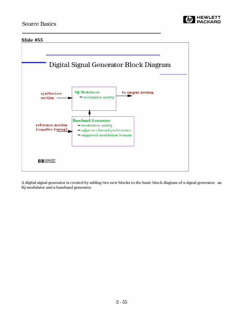
A digital signal generator is created by adding two new blocks to the basic block diagram of a signal generator: anIQ modulator and a baseband generator.
H
Digital Signal Generator Block Diagram
IQ Modulator
modulation quality
Baseband Generator
modulation quality
adjacent channel performance
supported modulation formats
reference section
(supplies timing)
to output sectionsynthesizer
section
2 - 55
HSource Basics
Slide #56
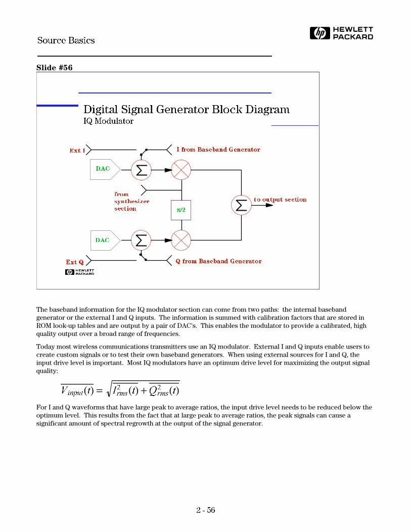
The baseband information for the IQ modulator section can come from two paths: the internal basebandgenerator or the external I and Q inputs. The information is summed with calibration factors that are stored inROM look-up tables and are output by a pair of DAC's. This enables the modulator to provide a calibrated, highquality output over a broad range of frequencies.
Today most wireless communications transmitters use an IQ modulator. External I and Q inputs enable users tocreate custom signals or to test their own baseband generators. When using external sources for I and Q, theinput drive level is important. Most IQ modulators have an optimum drive level for maximizing the output signalquality:
V input(t) = Irms
2 (t) +Qrms
2 (t)For I and Q waveforms that have large peak to average ratios, the input drive level needs to be reduced below theoptimum level. This results from the fact that at large peak to average ratios, the peak signals can cause asignificant amount of spectral regrowth at the output of the signal generator.
H
Digital Signal Generator Block DiagramIQ Modulator
ππ/2
DAC
DAC
Ext I
Ext Q
from
synthesizer
section
to output section
Q from Baseband Generator
I from Baseband Generator
2 - 56
HSource Basics

Slide #57
The baseband generator creates the baseband waveforms needed to drive the IQ modulator. The above blockdiagram provides three paths for supplying data for the baseband waveforms:
1. Data may be loaded from an external computer2. Data may be loaded directly from RAM3. TTL data may be input (this requires both a data clock and symbol clock)
The data is the raw "1's" and "0's" that will be used to construct the baseband signal. Datum are combined tomake symbols for modulation formats that require more than one bit per symbol. Filtering is added to increasethe bandwidth efficiency of the output signal. The filtering is done digitally. The digital stream is sent to a DAC.The output of the DAC's are sent to analog reconstruction filters. These filters are smoothing filters that removethe high frequency components of the waveforms that cause spectral spreading:
DAC
AnalogReconstruction
Filter
H
Digital Signal Generator Block DiagramBaseband Generator
DAC
DAC
AAAAAAAAAAAAAAAAAAAAAAAAAAAAAAAAAAAAAAAAAAAA
AAAAAAAAAAAAAAAAAAAAAAAAAAAAAAAAAAAAAAAAAAAA
AAAAAAAAAAA
Pattern RAM Constellation
Map and
Baseband
Filters
Timing
Data
Data Clock
Symbol
Clock
From CPU
I
Q
Analog
Reconstruction
Filters
2 - 57
HSource Basics

Slide #58
The table above illustrates the types of parameters that are specified for digital formats.
The combination of the baseband generator and the IQ modulator produce a digitally modulated signal. Thefiltering and modulation type are determined by the shape of the baseband waveforms.
To accurately simulate a digital signal, however, the signal generator must do more than just output the propermodulation. Most digital communication formats, in an effort to conserve bandwidth, have some access scheme.For US-TDMA (IS-54), the access scheme requires a separation in frequency between the forward, base to mobile,and reverse, mobile to base channels. In addition, the forward and reverse links are each allocated a specific sliceof time during which communication takes place: This is called Time Division Multiple Access or TDMA. This"slice of time" is generally referred to as a time slot.
The following formats are commonly found in digital signal generators:
1. GSM2. DECT3. Tetra4. US-TDMA (NADC, USDC, or IS-54)5. PDC6. PHS7. PHP8. CDMA (IS-95, wideband)
H
Digital Signal GeneratorDigital Signals
US-TDMA
Parameter Specification
Access Method TDMA/FDD
Modulation π/4 DQPSK
Channel Bandwidth 30 kHz
Reverse Channel
Frequency Band
824 - 849 MHz
Forward Channel
Frequency Band
869 - 894 MHz
Filtering 0.35 RRC
2 - 58
HSource Basics
Slide #59
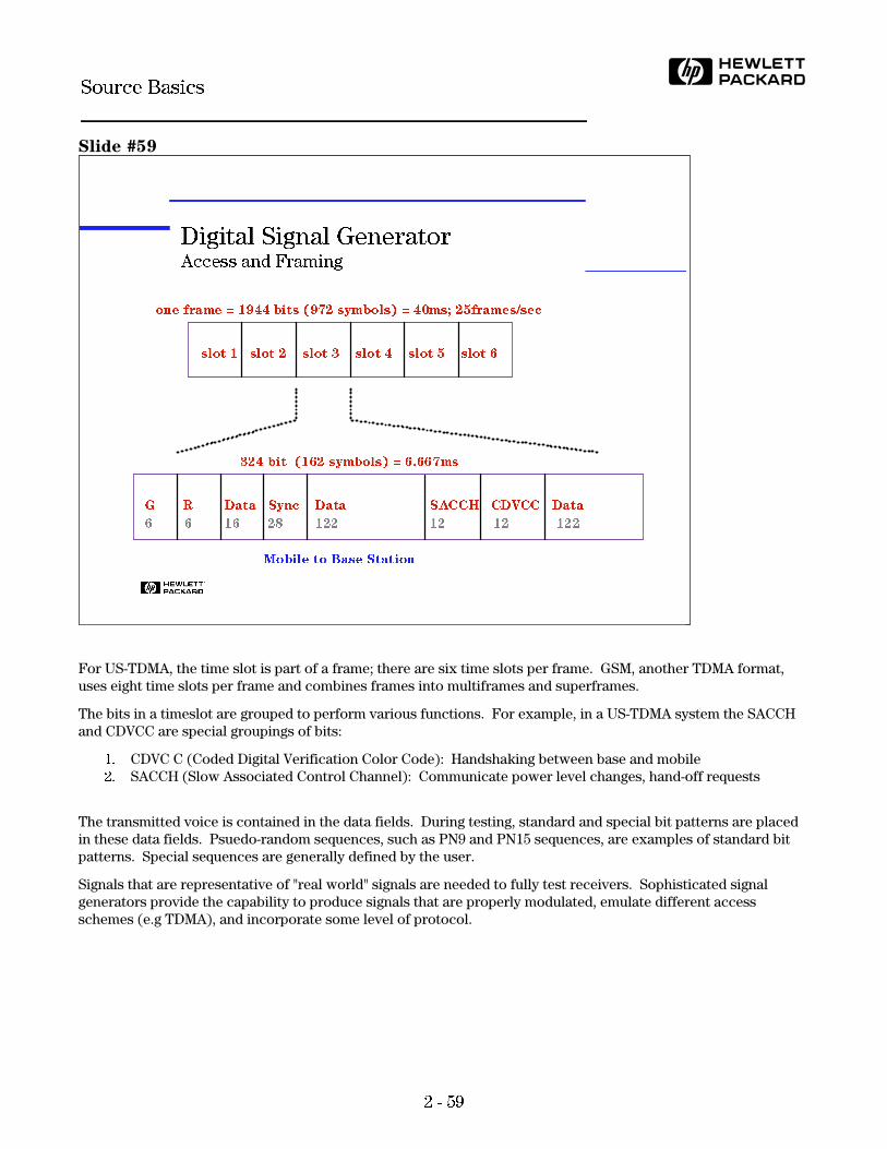
For US-TDMA, the time slot is part of a frame; there are six time slots per frame. GSM, another TDMA format,uses eight time slots per frame and combines frames into multiframes and superframes.
The bits in a timeslot are grouped to perform various functions. For example, in a US-TDMA system the SACCHand CDVCC are special groupings of bits:
1. CDVC C (Coded Digital Verification Color Code): Handshaking between base and mobile2. SACCH (Slow Associated Control Channel): Communicate power level changes, hand-off requests
The transmitted voice is contained in the data fields. During testing, standard and special bit patterns are placedin these data fields. Psuedo-random sequences, such as PN9 and PN15 sequences, are examples of standard bitpatterns. Special sequences are generally defined by the user.
Signals that are representative of "real world" signals are needed to fully test receivers. Sophisticated signalgenerators provide the capability to produce signals that are properly modulated, emulate different accessschemes (e.g TDMA), and incorporate some level of protocol.
H
Digital Signal GeneratorAccess and Framing
one frame = 1944 bits (972 symbols) = 40ms; 25frames/sec
slot 1 slot 2 slot 3 slot 4 slot 5 slot 6
324 bit (162 symbols) = 6.667ms
G R Data Sync Data SACCH CDVCC Data
6 6 16 28 122 12 12 122
Mobile to Base Station
2 - 59
HSource Basics

Slide #60
An entire seminar could be devoted to applications of signal generators. Signal generators are used to testreceivers as well as the components in a receiver. Sensitivity and selectivity are two receiver tests that arerequired by most standards. In addition to these two, other common receiver tests include:
1. Co-channel immunity2. Noise figure3. Intermodulation rejection
Most standards include detailed descriptions of how these tests are performed. Spectral regrowth is a commontransmitter and amplifier test.
When making any test, the specifications of the signal source must be analyzed to ensure that the source does notcorrupt the measurement. The critical specifications that a source must meet vary depending upon the test.
H
Applications and Critical SpecificationsAnalog and Digital
Receiver Sensitivity
frequency accuracy
level accuracy
error vector magnitude
Receiver Selectivity
phase noise
spurious
spectral accuracy
Spectral Regrowth
ACP performance
2 - 60
HSource Basics

Slide #61
The sensitivity of a receiver is the lowest possible signal level that can be reliably detected. Sensitivity is one ofthe key specifications for a receiver and is generally specified at a particular SINAD for FM receivers or BER forreceivers of digitally modulated signals. For FM receivers, SINAD is a figure of merit used to describe the usablesignal out of a receiver. SINAD is the ratio of the signal plus noise plus distortion to the noise plus distortion atthe same output:
SINAD = 10 log(S+N+DN+D )
The level of RF input required to maintain a SINAD of 12 dB is generally defined as the sensitivity of the receiverbecause this level provides a good quality audio signal. For receivers of digitally modulated signals, sensitivity isdefined as the level of the received signal that produces a specified BER when the signal is modulated with aspecified psuedo-random binary sequence (PRBS) of data.
The following critical signal generator specifications for measuring the sensitivity of a receiver will be discussed:
frequency accuracyamplitude (level) accuracyerror vector magnitude (for digitally modulated signals)
Frequency modulation deviation accuracy and frequency modulation distortion are two other specifications thataffect sensitivity measurements.
Poor frequency accuracy will cause the signal to fall nearer to the skirts of the filters in the receiver; this willdegrade the level of the signal and will reduce either the SINAD or BER measurement. A receiver will appear tohave a lower sensitivity when tested with a signal that has poor frequency accuracy.
H
Applications and Critical SpecificationsReceiver Sensitivity
Frequency Accuracy
frequency inaccuracy
amplitude inaccuracy
Want to measure
sensitivity in a channel
Measurement impaired
by frequency inaccuracy
DUT
input for
signal
generator
2 - 61
HSource Basics
Slide #62
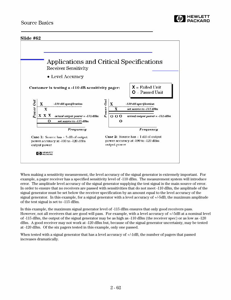
When making a sensitivity measurement, the level accuracy of the signal generator is extremely important. Forexample, a pager receiver has a specified sensitivity level of -110 dBm. The measurement system will introduceerror. The amplitude level accuracy of the signal generator supplying the test signal is the main source of error.In order to ensure that no receivers are passed with sensitivities that do not meet -110 dBm, the amplitude of thesignal generator must be set below the receiver specification by an amount equal to the level accuracy of thesignal generator. In this example, for a signal generator with a level accuracy of +/-5dB, the maximum amplitudeof the test signal is set to -115 dBm.
In this example, the maximum signal generator level of -115 dBm ensures that only good receivers pass.However, not all receivers that are good will pass. For example, with a level accuracy of +/-5dB at a nominal levelof -115 dBm, the output of the signal generator may be as high as -110 dBm (the receiver spec) or as low as -120dBm. A good receiver may not work at -120 dBm but, because of the signal generator uncertainty, may be testedat -120 dBm. Of the six pagers tested in this example, only one passed.
When tested with a signal generator that has a level accuracy of +/-1dB, the number of pagers that passedincreases dramatically.
H
Applications and Critical SpecificationsReceiver Sensitivity
Level Accuracy
Customer is testing a -110 dB sensitivity pager: X = Failed Unit
O = Passed Unit
FrequencyFrequency
PowerOut
PowerOut
X
X
X X X
X
X
O
O O O
O
-110 dB specification
actual output power = -114 dBm
set source to -115 dBm
-110 dB specification
set source to -111 dBm
actual output power = -112 dBm
Case 1: Source has ± 5 dB of output
power accuracy at -100 to -120 dBm
output power
Case 2: Source has ± 1 dB of output
power accuracy at -100 to -120 dBm
output power
2 - 62
HSource Basics

Slide #63
The best indicators of modulation quality are obtained from the constellation diagram of a signal. For phase shiftkeyed signals, the EVM measures the signal quality. For frequency shift keyed signals, the signal phase error is amore appropriate measurement. For amplitude shift keyed signals, magnitude error should be used.
For the above TETRA signal, the EVM is less than one percent. The size of the dots indicates the quality of thesignal: A signal with a larger EVM would have larger dots.
H
Applications and Critical SpecificationsReceiver Sensitivity
Error Vector Magnitude
e.g. TETRA Signal
p/4 DQPSK
EVM < 1.0%
EVM Spec
2 - 63
HSource Basics

Slide #64
Adjacent and alternate channel selectivity measures the receiver's ability to process a desired signal whilerejecting a strong signal in an adjacent channel or alternate channel. This test is very important forcommunication receivers where channel spacings are narrow and many signals may be encountered in a smallgeographical area. An adjacent or alternate channel selectivity test setup is shown above. One signal generatorinputs a test signal at the desired channel frequency at a level above the sensitivity of the receiver. The secondsignal generator outputs either the adjacent channel signal, offset by one channel spacing, or the alternate channelsignal, offset by two channel spacings. The output of the out-of-channel signal is increased until the sensitivity isdegraded to a specified level.
Frequency and amplitude (level) accuracy and the spectral characteristics of the test and interfering signal areimportant.
Poor frequency accuracy will cause the signals to be either too close or too far from each other and from the filterskirts. This can have the affect of appearing to improve or degrade the receiver performance.
We saw how level accuracy can affect the sensitivity measurement of a receiver. With two signals, the problemsassociated with inaccurate signals are compounded.
For FM receivers, the SSB phase noise of the interfering signal is the most critical spectral characteristic. Thetest is a measure of the performance of the receiver's IF filters. As the signal in the adjacent-channel is increased,the rejection of the IF filter outside the passband is eventually exceeded. If the phase noise energy inside thepassband is detected, the receiver may appear to fail the test.
High levels of spurs can also degrade the selectivity measurement of a receiver. Signal generator spurs that fallwithin the passband of the receiver will contribute to the overall noise level in the passband.
H
Applications and Critical SpecificationsReceiver Selectivity
IFRejectionCurve
Frequency
Level(dBm
)spur from source and/or high
levels of phase noise can cause a
good receiver to fail
IFsignal
in-channel signal
(modulated signal)
out-of-channel signal
(CW or modulated signal) DUT
Phase Noise
Spurious
2 - 64
HSource Basics

Slide #65
When measuring selectivity on receivers designed for digital signals, the most important spectral characteristic isspectral accuracy. With digital signals, the modulation sidebands are often wider than the channel spacings.These sidebands have considerably higher power at adjacent and alternate channel offsets than analog FMsignals. Because of this, the phase noise and the spurious of the signal generator is much less important.
However, the spectral shape is very important. For the adjacent-channel interferer, the spectral shape should beexact. EVM is a good indicator of the spectral shape within the modulation bandwidth of a signal. However, evenwith a good EVM, a signal may have a significant amount of spectral splatter outside of the modulationbandwidth. Comparing the measured adjacent-channel power (ACP) to the theoretical ACP provides anindication of the spectral quality outside of the modulation bandwidth.
H
Applications and Critical SpecificationsReceiver Selectivity
GSM Signal
0.3GMSK
Spectral Accuracy:
EVM
ACP
2 - 65
HSource Basics

Slide #66
Spectral regrowth is a common amplifier test. When stimulated with a digitally modulated signal, thenonlinearities in amplifiers create shoulders in the output spectrum. These shoulders are referred to as spectralregrowth. Spectral regrowth is related to intermodulation distortion. Intermodulation distortion results from theinteraction between two (or more) input sine waves. A digitally modulated signal can be expressed as an infinitesum of sine waves with properly weighted coefficients:
V(t) =n=1Σ ansin(2πfnt)
The interaction of these sine waves produces the spectral regrowth.
Signal generators have amplifiers that can also introduce spectral regrowth. When measuring an amplifier, thespectral regrowth, or ACP performance, of the signal generator should be less than that of the amplifier undertest.
H
Applications and Critical SpecificationsSpectral Regrowth
Input from signal generator
Output from amplifier
DUT
ACP Performance
2 - 66
HSource Basics

Slide #67
This seminar reviewed the basics of sources. Aspects of the design, specification, and application of sourceswere explored. A brief list of some of the reference material has been inlcuded for further study. In addition,Hewlett-Packard has an extensive library of application notes that provide more information on how to usesources.
H
Summary
Types of sources
CW
Swept
Signal Generator
Summary
2 - 67
HSource Basics

References
Adam, Stephen F., Microwave Theory and Applications, Prentice-Hall, Inc., Englewood Cliffs, New Jersey, 1969.
Clarke, Kenneth K., and Donald T. Hess, Communication Circuits: Analysis and Design, Addison-WesleyPublishing Company, Reading, Massachusetts, 1971
Kurzenknabe, Glenn R., Practical Considerations in Specification of High Stability Crystal Oscillators.
Peebles, Peyton Z., Jr., Probability, Random Variables, and Random Signal Principles, McGraw-Hill BookCompany, New York, 1980.
Rappaport, Theodore S., Wireless Communications, Prentice Hall PTR, Upper Saddle River, New Jersey, 1996.
Robins, W.P., Phase Noise in Signal Sources, Peter Peregrinus Ltd, London, UK., 1984.
Taub, Herbert, and Donald L. Schilling, Principles of Communication Systems, 2nd ed.,McGraw-Hill BookCompany, New York, 1986.
Test and Measurement Catalog 1997, Hewlett-Packard Company.
2 - 68
HSource Basics

Date Subject to Change
Copyright 1997
Hewlett-Packard Company
Printed in U.S.A. 4/97
5965-7918E