max16031 ev kit - maxim integratedu1 1 maxim eeprom-based system monitor max16031etm+ (48-pin tqfn)...
TRANSCRIPT

General DescriptionThe MAX16031 evaluation kit (EV kit) provides a provenprinted-circuit board (PCB) layout that facilitates evalu-ation of the MAX16031 EEPROM-based system monitorwith nonvolatile fault memory. This EV kit is a fullyassembled and tested surface-mount board.
The EV kit includes an on-board USB-to-JTAG and I2Cinterface facilitating communications between the hostPC and the MAX16031. A DAC connected to the moni-toring inputs and the status LEDs connected to eachprogrammable output make it easy to evaluate the vari-ous monitoring functions of the MAX16031.
This EV kit data sheet assumes basic familiarity with theMAX16031. Refer to the MAX16031/MAX16032 IC datasheet for more detailed information.
Features♦ USB Interface to Host PC
♦ Easy-to-Use GUI Software
♦ Facilitates Programming of MAX16031s onPrototype Boards
♦ LEDs Indicate Each Output’s State
♦ On-Board DAC Simulates Monitored Voltages
♦ Convenient Test Points and Headers for EasyEvaluation
♦ Fully Assembled and Tested
Eva
lua
tes: M
AX
16
03
1
MAX16031 Evaluation Kit
________________________________________________________________ Maxim Integrated Products 1
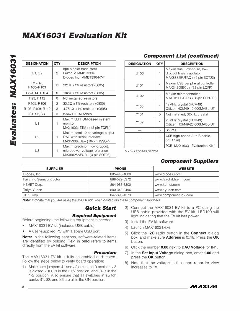
DESIGNATION QTY DESCRIPTION
C1, C2, C4, C100, C108
5
1μF ±10%, 10V X5R ceramic capacitors (0805) TDK C2012X5R1A105K KEMET C0805C105K4PAC
C3, C5, C6 3
0.1μF ±10%, 25V X7R ceramic capacitors (0805) TDK C2012X7R1E104K Taiyo Yuden TMK212B104KT
C7 0 Not installed, capacitor (0805)
C101, C102, C103
3
0.1μF ±10%, 25V X7R ceramic capacitors (0603) TDK C1608X7R1E104K Taiyo Yuden TMK107BJ104KA
C104, C105, C106, C107
4
18pF ±5%, 50V C0G ceramic capacitors (0603) TDK C1608C0G1H180J Taiyo Yuden UMK107CG180JZ
C110 1
4.7μF ±20%, 6.3V X5R ceramic capacitor (0805) TDK C2012X5R0J475M Taiyo Yuden JMK212BJ475MG
C111 1
0.01μF ±10%, 50V X7R ceramic capacitor (0603) TDK C1608X7R1H103K Taiyo Yuden UMK107B103KZ
DESIGNATION QTY DESCRIPTION
C112, C113 2
2.2µF ±20%, 10V X5R ceramiccapacitors (0805)TDK C2012X5R1A225MTaiyo Yuden LMK212BJ225MG
C114 1
33pF ±5%, 50V C0G ceramiccapacitor (0603)TDK C1608C0G1H330JTaiyo Yuden UMK107CG330JZ
EXT PWR 1 Test point, red
F100 1 500mA fast-acting fuse (2405)
GND, REF 2 Test points, black
J1, J2, J4 3 3-pin headers
J3 1 2-pin header
J100 1 2 x 3-pin header
LED1–LED7,LE D 100–LE D 103
11 Green LEDs (1206)
P100 1 USB_B right-angle connector
P101, P102 0 Not installed
P1 1 5-pin header
P2 1 2 x 5-pin header
P3 1 11-pin header
P4 1 9-pin header
P5 1 4-pin header
Component List
Ordering Information
19-1540; Rev 0; 11/07
For pricing, delivery, and ordering information, please contact Maxim Direct at 1-888-629-4642,or visit Maxim’s website at www.maxim-ic.com.
+Denotes lead-free and RoHS-compliant.
PART TYPE
MAX16031EVKIT+ EV Kit
Eva
lua
tes:
M
AX
16
03
1
MAX16031 Evaluation Kit
2 _______________________________________________________________________________________
DESIGNATION QTY DESCRIPTION
Q1, Q2 2 npn bipolar transistors Fairchild MMBT3904 Diodes Inc. MMBT3904-7-F
R1–R7, R100–R103
11 221 ±1% resistors (0805)
R8–R14, R104 8 10k ±1% resistors (0805)
R23, R112 0 Not installed, resistors
R105, R106 2 33.2 ±1% resistors (0805)
R108, R109, R110 3 4.75k ±1% resistors (0805)
S1, S2, S3 3 8-row DIP switches
U1 1 Maxim EEPROM-based system monitor MAX16031ETM+ (48-pin TQFN)
U2 1 Maxim octal 12-bit voltage-output DAC with serial interface MAX5306EUE+ (16-pin TSSOP)
U3 1 Maxim precision, low-dropout, micropower voltage reference MAX6025AEUR+ (3-pin SOT23)
DESIGNATION QTY DESCRIPTION
U100 1 Maxim dual, low-noise, low-dropout linear regulator MAX8882EUTAQ+ (6-pin SOT23)
U101 1 Maxim USB peripheral controller MAX3420EECJ+ (32-pin LQFP)
U102 1 Maxim microcontroller MAXQ2000-RAX+ (68-pin QFN-EP*)
Y100 1 12MHz crystal (HCM49) Citizen HCM49-12.000MABJ-UT
Y101 0 Not installed, 32kHz crystal
Y102 1 20MHz crystal (HCM49) Citizen HCM49-20.000MABJ-UT
— 5 Shunts
— 1 USB high-speed A-to-B cable, 5ft (1.5m)
— 1 PCB: MAX16031 Evaluation Kit+
Component List (continued)
SUPPLIER PHONE WEBSITE
Diodes, Inc. 805-446-4800 www.diodes.com
Fairchild Semiconductor 888-522-5372 www.fairchildsemi.com
KEMET Corp. 864-963-6300 www.kemet.com
Taiyo Yuden 800-348-2496 www.t-yuden.com
TDK Corp. 847-390-4373 www.component.tdk.com
Component Suppliers
Note: Indicate that you are using the MAX16031 when contacting these component suppliers.
Quick StartRequired Equipment
Before beginning, the following equipment is needed:
• MAX16031 EV kit (includes USB cable)
• A user-supplied PC with a spare USB port
Note: In the following sections, software-related itemsare identified by bolding. Text in bold refers to itemsdirectly from the EV kit software.
ProcedureThe MAX16031 EV kit is fully assembled and tested.Follow the steps below to verify board operation:
1) Make sure jumpers J1 and J2 are in the 0 position, J3is closed, J100 is in the 3.3V position, and J4 is in the1-2 position. Also ensure that all switches in switchbanks S1, S2, and S3 are all in the ON position.
2) Connect the MAX16031 EV kit to a PC using theUSB cable provided with the EV kit. LED100 willlight indicating that the EV kit has power.
3) Install the EV kit software.
4) Launch MAX16031.exe.
5) Click the I2C radio button in the Connect dialogbox, and make sure Address is 0x18. Press the OKbutton.
6) Click the number 0.00 next to DAC Voltage for IN1.
7) In the Set Input Voltage dialog box, enter 1.00 andpress the OK button.
8) Note that the voltage in the chart-recorder viewincreases to 1V.
*EP = Exposed paddle.

Detailed Description of SoftwareConnecting to the MAX16031 EV Kit
Make sure the EV kit is connected to the PC by the USBcable. Launch the software and in the Connect dialog(Figure 1), select the I2C or JTAG radio button andclick OK. If the software is being used without the EV kitconnected, select the Demo (No Hardware Required)radio button.
The I2C slave address may be specified. The default is0x18, but other values (depending on the settings ofjumpers J1 and J2) can be used.
Voltages TabThe Voltages tab (Figure 2) provides a visual indicationof the voltage present on every IN_ input. Each channelhas a settings dialog (accessed by clicking the under-lined IN_ link), a DAC output voltage setting, settingsfor each overvoltage and undervoltage threshold, twofault flags, and a chart-recorder view.
Eva
lua
tes: M
AX
16
03
1
MAX16031 Evaluation Kit
_______________________________________________________________________________________ 3
Figure 1. Connect Dialog
Figure 2. Voltages Tab

Eva
lua
tes:
M
AX
16
03
1
MAX16031 Evaluation Kit
4 _______________________________________________________________________________________
The Settings dialog (Figure 3) can set the IN input-volt-age range to one of three settings: 1.4V, 2.8V, and5.6V. To enable channel monitoring, make sure theEnable Fault Detection checkbox is selected. TheDisable Interrupts and Outputs for group box allowsfaults on the primary or secondary thresholds to be“masked,” which prevents them from triggering anSMBus™ interrupt or asserting a fault output. The SaveState to EEPROM on group box selects which type offault can trigger a nonvolatile fault save operation.
Each IN_ input can be connected to the on-boardMAX5306 DAC using switch bank S1. This allows thevoltage at the IN_ input to be manually controlled throughthe EV kit software. Click the link next to DAC Voltage toset the voltage of the DAC in the 0 to 2.5V range. TheDAC voltage can also be changed by dragging the dot-ted green line, shown in the chart-recorder view.
To set the primary or secondary overvoltage or under-voltage thresholds for a particular channel, click theappropriate underlined number next to that parameter.The primary thresholds can also be modified by drag-ging the dotted red lines in the chart-recorder view. Thesecondary thresholds can be changed the same way;both appear as dotted yellow lines.
Two fault flag indicators are associated with each chan-nel. The upper one corresponds to the primary faultthresholds; the lower one corresponds with the sec-ondary fault thresholds. If an undervoltage or overvolt-age fault occurs, one or both these indicators will turnred and remain so even after the original fault conditionis removed. To clear a fault indicator, click the indicatorand select Clear Fault or Clear All Faults on the menuthat appears.
Each chart-recorder view shows the voltage on the cor-responding IN_ input with a solid green line. To zoom inand zoom out, click the magnifying glass icons in theupper right of the chart-recorder view. Another way tozoom in and out is to click and “drag” a selection rec-tangle. Drag from upper left to lower right to zoom in,and from lower right to upper left to zoom out.
Two IN inputs can be paired to form a combined differ-ential input. Click any of the Single Ended links in thecenter of the window to pair two inputs together, or toseparate two paired inputs.
Figure 3. Settings Dialog
SMBus is a trademark of Intel Corp.

Eva
lua
tes: M
AX
16
03
1
MAX16031 Evaluation Kit
_______________________________________________________________________________________ 5
Figure 4. Current and Temperature Tab
Current and Temperature TabThe Current and Temperature tab (Figure 4) providesa set of chart-recorder views similar to the Voltagestab. To select the display units for the temperature sen-sors, click the appropriate setting of the TemperatureDisplay radio buttons.
Similar to the input channels on the Voltages tab, thecurrent and the temperature channels each have a set-tings dialog. Click the title of each channel to display
the settings dialog. To enable channel monitoring,make sure Enable Fault Detection is selected (Figure5). The Disable Interrupts and Outputs for group boxallows faults on the primary or secondary thresholds tobe “masked,” which prevents them from triggering anSMBus interrupt or asserting a fault output. The SaveState to EEPROM on group box controls whether afault can trigger a nonvolatile fault save operation.
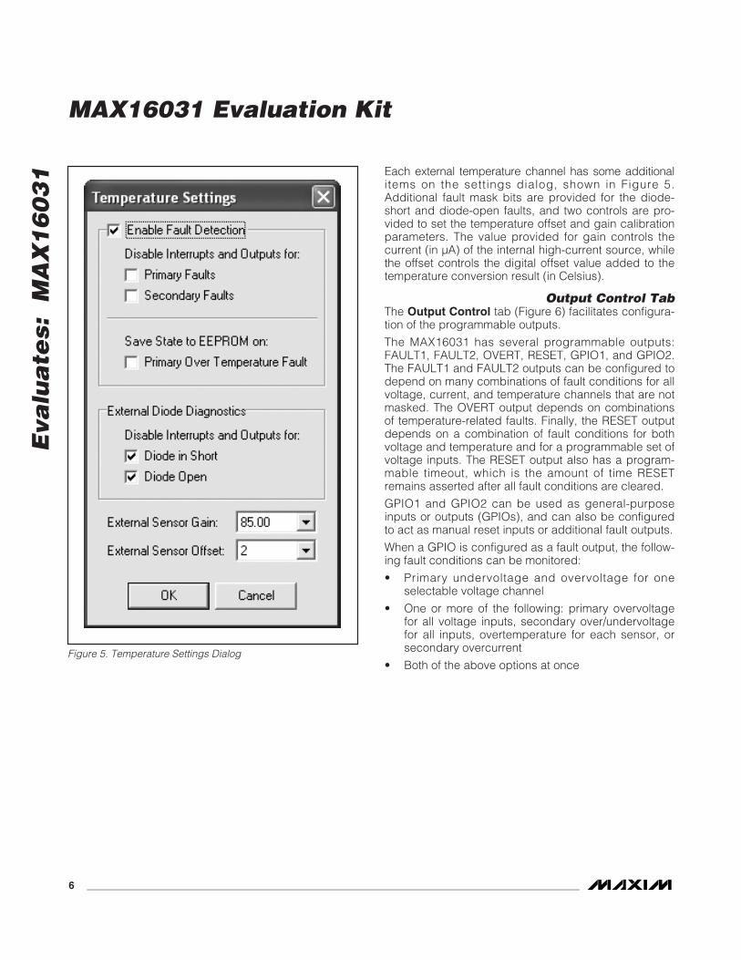
Each external temperature channel has some additionalitems on the settings dialog, shown in Figure 5.Additional fault mask bits are provided for the diode-short and diode-open faults, and two controls are pro-vided to set the temperature offset and gain calibrationparameters. The value provided for gain controls thecurrent (in µA) of the internal high-current source, whilethe offset controls the digital offset value added to thetemperature conversion result (in Celsius).
Output Control TabThe Output Control tab (Figure 6) facilitates configura-tion of the programmable outputs.
The MAX16031 has several programmable outputs:FAULT1, FAULT2, OVERT, RESET, GPIO1, and GPIO2.The FAULT1 and FAULT2 outputs can be configured todepend on many combinations of fault conditions for allvoltage, current, and temperature channels that are notmasked. The OVERT output depends on combinationsof temperature-related faults. Finally, the RESET outputdepends on a combination of fault conditions for bothvoltage and temperature and for a programmable set ofvoltage inputs. The RESET output also has a program-mable timeout, which is the amount of time RESETremains asserted after all fault conditions are cleared.
GPIO1 and GPIO2 can be used as general-purposeinputs or outputs (GPIOs), and can also be configuredto act as manual reset inputs or additional fault outputs.
When a GPIO is configured as a fault output, the follow-ing fault conditions can be monitored:
• Primary undervoltage and overvoltage for oneselectable voltage channel
• One or more of the following: primary overvoltagefor all voltage inputs, secondary over/undervoltagefor all inputs, overtemperature for each sensor, orsecondary overcurrent
• Both of the above options at once
Eva
lua
tes:
M
AX
16
03
1
MAX16031 Evaluation Kit
6 _______________________________________________________________________________________
Figure 5. Temperature Settings Dialog

Miscellaneous TabMany other configuration options are available in theMiscellaneous tab (Figure 7): the boot-up delay, thetemperature filter, overcurrent settings, deglitch set-tings, fault settings, memory lock bits, and the SMBusalert configuration.
The After-boot timeout setting controls the time delayfrom when power is applied, to when monitoring isenabled. This can prevent a partially powered systemfrom triggering false fault signals during startup.
The Temp sense filter time constant provides theability to filter the temperature sensors to reduce noise.
Overcurrent settings include OC timeout, which con-trols the amount of time a secondary overcurrent condi-tion must be present before it triggers a fault, and OCoutput pin, which controls whether the OVERC outputlatches an overcurrent fault or follows the state of theprimary overcurrent comparator.
Filtering of the voltage-monitoring channels is con-trolled by the Hysteresis of all thresholds setting,which sets the voltage difference between the risingand falling voltage threshold of each fault comparator.Require 2 faults in a row, when turned on, preventsany voltage fault from occurring unless the fault condi-tion is present for two complete ADC conversion cyclesin a row.
Eva
lua
tes: M
AX
16
03
1
MAX16031 Evaluation Kit
_______________________________________________________________________________________ 7
Figure 6. Output Control Tab

Eva
lua
tes:
M
AX
16
03
1 The On major fault setting controls what information issaved to the fault EEPROM during a fault condition.Save only fault flags means that only the fault flagsare stored to EEPROM during a fault event; Save faultflags and ADC means that both the fault flags and theADC readings for all channels are stored to EEPROMduring a fault event.
Version code provides user access to register 5Eh.This register does not control any function of the chip,but can be used to store user-defined data such as aversion number.
The registers and the configuration EEPROM can belocked with the Configuration setting to prevent unin-tentional modification of configuration settings. The lockicon in the lower-left corner of the window also indi-cates and controls this lock bit.
The fault EEPROM is locked automatically when a faultcondition occurs and must be unlocked before anysubsequent fault will get stored to EEPROM. Unlock itusing the ADC-related EEPROM lock setting.
To enable full SMBus functionality and allow theSMBALERT output to assert, the SMBALERT# Signaloption must be enabled.
MAX16031 Evaluation Kit
8 _______________________________________________________________________________________
Figure 7. Miscellaneous Tab

Registers TabBesides the easy-to-use GUI controls, the MAX16031can also be configured by directly modifying the regis-ters and EEPROM. The Registers tab (Figure 8) pro-vides access to the registers and EEPROM. Modify aregister by clicking the cell under the Value column,entering the new value, and pressing Enter or clickingin another cell.
Most configuration registers have a matching EEPROMlocation that is copied to the register when theMAX16031 powers up. The Registers tab places eachpair on the same row. After experimenting with a partic-ular register configuration, that configuration can bewritten to the EEPROM by clicking the CommitConfiguration to EEPROM button.
Eva
lua
tes: M
AX
16
03
1
MAX16031 Evaluation Kit
_______________________________________________________________________________________ 9
Figure 8. Registers Tab

Eva
lua
tes:
M
AX
16
03
1 Menu ReferenceSystem
Connect... directs the software to open a connectionwith a connected EV kit and brings up the Connectdialog (Figure 1) to select the connection type. Onceconnected, this menu item changes to Disconnect.
Save as SVF… writes the EEPROM configuration to anSVF file, which is a standard format used by JTAGdevice programmers for production programming.
Save Configuration… and Load Configuration…save and load the register and EEPROM configurationto a text file.
PollingOn and Off turn register polling on and off. Whenpolling is on, the controls in all the tabs are periodicallyrefreshed from the physical registers. If polling is off,register content can be read from the device by select-ing Read All Registers.
AboutThis menu item launches the About dialog, which dis-plays the software version, whether the EV kit is connect-ed, and the firmware revision of the USB interface.
SMBus Alert FunctionalityWhen the SMBALERT# signal is enabled using theoption in the Miscellaneous tab, any fault that occurswill cause this signal to be asserted. When that hap-pens, the status bar displays SMBALERT# detected.Click here to send Alert Response Address. Clickingthe status bar item then causes the EV kit hardware toissue an Alert Response Address command, whichreturns the slave address of the SMBus device that trig-gered the SMBus alert.
Detailed Description of HardwareThe MAX16031 monitors eight voltages, three tempera-tures, and one current. Seven configurable outputsindicate fault-status information. Figure 9 provides anoverview of the major features of the EV kit PCB.
MAX16031 Evaluation Kit
10 ______________________________________________________________________________________
P3
R23
LED1–LED7
P4
J1J2
Q2 Q1
P5
J3
S1
S2
S3P2
P1
J4
USB
J100
LED100
LED103LED102LED101
1-800-737-7600 WWW.MAXIM-IC.COMMAX16031 EVALUATION KIT+
EXTPWRGND
CONNECTEDACTIVITY
EEPROM
POWER
VCC SELECT
EXTERNAL POWERSUPPLY
(OPTIONAL)
MONITORED INPUTS
CURRENT-SENSERESISTOR
(OPTIONAL)
CURRENT-SENSEBIAS
JTAG
I2C PULLUPVOLTAGESELECT
OUTPUTS
OUTPUTSTATUSINDICATORSTEMPERATURE
SENSORS
TEMPERATURE-SENSOR CONNECTIONS
CONNECTS DACOUTPUTS TOMONITORING
INPUTS CONFIGURESJTAG AND I2CBUS ROUTING
I2C ADDRESS SELECT
MAX16031
Figure 9. Evaluation Kit PCB Diagram

USB-Host InterfaceThe MAX16031 EV kit includes a built-in USB-to-JTAG/I2C host interface. The host interface usesMaxim’s MAX3420 USB peripheral controller, alongwith a MAXQ2000 microcontroller to communicate withthe host PC and generate the I2C/JTAG bus signals.Three indicators (LED101, LED102, LED103) providestatus information of the host interface. LED101 lightsduring EEPROM write operations, LED102 lights duringI2C or JTAG bus activity, and LED103 lights when thesoftware is communicating to the EV kit.
To facilitate prototype development and programming,the host interface can be used to interface with aMAX16031 on another board by turning off switches 1-7 in switch bank S2. This disconnects the on-boardMAX16031 from the JTAG and I2C buses. Connect tothe other board using P1 and P2. The pinout of eachconnector is shown in Tables 2 and 3. Note that the I2Cpullup resistors are located on the EV kit.
The on-board MAX16031 can be connected to anexternal JTAG or I2C interface by turning switch bankS3 (switches 1-7) off while keeping switch bank S2(switches 1-7) on. Connect the external interface to P2for JTAG or P1 for I2C. The MAX16031 can be com-pletely disconnected from the on-board USB host inter-face by using this technique, while providing externalpower to EXT PWR (J100 must be in the EXT position),and disconnecting the on-board DACs by turning off allthe switches in switch bank S1.
Each interface can be disconnected or connected sep-arately. I2C uses switches 1-3 on both S2 and S3 whileJTAG uses switches 4-7 on both S2 and S3.
Power SourceThe MAX16031 IC can be powered from one of threepossible power supplies, controlled by jumper J100. Topower directly from the USB 5V supply, place thejumper in the 5V position. To power from the on-board3.3V regulator, place the jumper in the 3.3V position.When the jumper is in the EXT position, the MAX16031can be powered from an external power supply con-nected to the EXT PWR test point. Do not supply a volt-age higher than 14V.
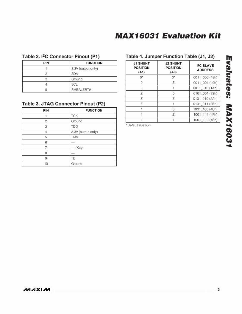
Serial InterfacesThe MAX16031 has both a JTAG interface and an I2Cserial interface. The slave address of the on-boardMAX16031 can be set using J1 and J2, according toTable 4.
Voltage MonitoringThe eight voltage monitoring inputs connect to pins onP3 located on the left side of the board. Switch bank S1allows each input to be connected to the output of aDAC, which allows the voltage to be set using the EV kitsoftware for ease of evaluation. The DAC output voltagerange is limited to 2.5V. Do not attempt to force anexternal voltage while the DAC is connected; doing socould damage the DAC or the external voltage source.
Current MonitoringThe current-sense inputs are connected to pins onheader P3 and can be used in two ways. A small volt-age source can be applied directly across CS+ andCS-, which the MAX16031 will measure directly. For thissituation, J3 must be closed, which connects CS+ toVCC to ensure proper bias. As an alternative, a current-sense resistor can be soldered in the R23 position andCS+ and CS- can be connected in series with theexternal circuit to be measured.
If an external bias voltage is to be used, remove J3 andconnect the CS+ pin of P3 to the external source. Donot supply a bias voltage higher than 28V. The current-sense circuit in the MAX16031 will not function for biasvoltages less than 3V.
Temperature MonitoringOne of the temperature sensors is internal and theother two are external. Both external temperature sen-sors are included on the EV kit as Q1 and Q2, whichare diode-connected 2N3904 transistors. These can bedesoldered and replaced if necessary. The connec-tions are easily accessible through header P5.
Inputs and OutputsEach output has a separate indicator LED and pullupresistor, and each signal is brought out to a pin on P4.An LED will light to indicate that the associated outputhas gone to the logic-low state. The LEDs can be dis-abled by turning off switch 8 in switch bank S2. Thepullup resistors are controlled by J4. To use an externalpullup voltage, connect J4 in the 2-3 position and con-nect the voltage source to the VPU pin of P4.
GPIO1 and GPIO2 can also function as inputs. If theyare configured as such, connect the external input tothe GPIO1 or GPIO2 pin of P4.
A test point (REF) is provided to confirm the referencevoltage of the MAX16031, which is 1.4V (nominal). Donot connect loads to this test point.
Eva
lua
tes: M
AX
16
03
1
MAX16031 Evaluation Kit
______________________________________________________________________________________ 11

Eva
lua
tes:
M
AX
16
03
1
MAX16031 Evaluation Kit
12 ______________________________________________________________________________________
JUMPER POSITION FUNCTION
5V* MAX16031 powered from 5V USB power
3.3V MAX16031 powered from 3.3V regulator J100
EXT MAX16031 powered from EXT PWR test point
Open Current-sense amplifier biased externally (CS+ test point) J3
Closed* Current-sense amplifier biased from MAX16031 VCC
1-2* Output pullup resistors connected to 3.3V J4
2-3 Output pullup resistors connected to VPU test point
1 Connects IN1 to DAC channel 1 when closed
2 Connects IN2 to DAC channel 2 when closed
3 Connects IN3 to DAC channel 3 when closed
4 Connects IN4 to DAC channel 4 when closed
5 Connects IN5 to DAC channel 5 when closed
6 Connects IN6 to DAC channel 6 when closed
7 Connects IN7 to DAC channel 7 when closed
S1
8 Connects IN8 to DAC channel 8 when closed
1
2
3
Connects P1 (I2C) to on-board MAX16031 when closed
4
5
6
7
Connects P2 (JTAG) to on-board MAX16031 when closed
S2
8 Enables output LEDs when closed
1
2
3
Connects I2C bus of host interface to P1 when closed
4
5
6
7
Connects JTAG bus of host interface to P2 when closed
S3
8 Not used
Table 1. Jumper Function Table (J100, J3, J4, S1, S2, S3)
*Default position.
Jumper Function Tables
Eva
lua
tes: M
AX
16
03
1
MAX16031 Evaluation Kit
______________________________________________________________________________________ 13
PIN FUNCTION
1 3.3V (output only)
2 SDA
3 Ground
4 SCL
5 SMBALERT#
Table 2. I2C Connector Pinout (P1)
PIN FUNCTION
1 TCK
2 Ground
3 TDO
4 3.3V (output only)
5 TMS
6 —
7 — (Key)
8 —
9 TDI
10 Ground
Table 3. JTAG Connector Pinout (P2)
J1 SHUNT POSITION
(A1)
J2 SHUNT POSITION
(A0)
I2C SLAVE ADDRESS
0* 0* 0011_000 (18h)
0 Z 0011_001 (19h)
0 1 0011_010 (1Ah)
Z 0 0101_001 (29h)
Z Z 0101_010 (2Ah)
Z 1 0101_011 (2Bh)
1 0 1001_100 (4Ch)
1 Z 1001_111 (4Fh)
1 1 1001_110 (4Eh)
Table 4. Jumper Function Table (J1, J2)
*Default position.

Eva
lua
tes:
M
AX
16
03
1
MAX16031 Evaluation Kit
14 ______________________________________________________________________________________
43
Q2 MM
BT39
04Q1
MM
BT39
04
DXN2
44DX
P245
DXN1
46DX
P1
48IN
11
IN2
2IN
33
IN4
9IN
510
IN6
11IN
712
IN8
41CS
-42
CS-
CS+
CS+
14GP
IO1
15GP
IO2
22OV
ERT
23OV
ERC
24FA
ULT1
25FA
ULT2
26RE
SET
17SD
A18
SCL
19A0
20A0 A1
A1
28TC
K29
TDI
33TD
O
27TM
S
21AL
ERT
47N.C.
40N.C.
39N.C.
32N.C.
31N.C.
35GND
13GND
8GND
30N.C.
7N.C.
6N.C.
5N.C.
4N.C.
16 RBP
34 DBP
38 V CC
37 V CC
MAX
1603
1
U1
MAX
6025
U3
MAX
5306
U2
1 2 3 4 5 6 7 8
16 15 14 13 12 11 10 9
S2
EXT
SEL
910
1112
1314
1516
87
65
43
21
S1SW
DIP
-8
R1 221Ω
1%
R2 221Ω
1%
R3 221Ω
1%
R4 221Ω
1%
R5 221Ω
1%
R6 221Ω
1%
R7 221Ω
1%
LED1
LED2
LED3
LED4
LED5
LED6
LED7
R23
RES1
R8 10kΩ
1%
R9 10kΩ
1%
R10
10kΩ
1%
R11
10kΩ
1%
R12
10kΩ
1%
R13
10kΩ
1%
R14
10kΩ
1%
J4
+3.3
VPUS
EL
+3.3
+3.3
2 4 6 8 10
1 3 5 7 9
JTAGP2
54
32
1
P1 I2 C
1 2 3 4
1 2 3 4
CON4P5
1 2CS
-CS
+3 4 5 6 7 8 9
1 2 3 4 5 6 7 8 910 11
10 11
CON1
1
P3
9 8 7 6 5 4 3 2 1
9 8 7 6 5 4 3 2 1
CON9P4
1 2 3 4 5 6 7 8
16 15 14 13 12 11 10 9
S3
PC S
EL
TDO
TDI
TCK
TMS
DIN
LDAC
DCLKCS
SCL
SDA
ALER
T
C3 0.1μ
F REF
36 ABP
C4 1μF
VBP
VCC
C2 1μF
C1 1μF
J3 CSBI
AS
VCC
16CS
1SC
LK2
DIN
15DO
UT3
LDAC
5OU
T16
OUT2
7OU
T38
OUT4
9OU
T510
OUT6
11OU
T712
OUT8
42
REF
13
GND
14 VDD
OUT
1IN
3
GND
C5 0.1μ
F
+3.3
+3.3
C7 NPC6 0.
1μF
VBP
J1 A1
A1J2 A0
A0
12
3
Figure 10. MAX16031 EV Kit Schematic

Eva
lua
tes: M
AX
16
03
1
MAX16031 Evaluation Kit
______________________________________________________________________________________ 15
MAXQ2000-RAX
U102
53P7.1/RX0/INT15
52RX0TX0
P7.0/TX0/INT1448
P6.5/T0/WKOUT147
P6.4/T0B/WKOUT046
P6.3/T2/OW_IN45
P6.2/T2B/OW_OUT44
P6.1/T1/INT13
41P5.7/MISO
40P5.6/SCLK
39P5.5/MOSI
38
MISOSCLKMOSISS
P5.4/SS
32P4.3/TDO
31P4.2/TMS
30P4.1/TDI/INT9
36P5.2/RX1/INT10
63SEG5/P0.5/INT1SEG4/P0.4/INT0
62
43RESUSBINT
P6.0/T1B/INT12
37P5.3/TX1/INT11
29P4.0/TCK/INT8
21SEG31/P3.7/INT7
18SEG28/P3.4/INT4
17SEG27/P3.3
16SEG26/P3.2
19SEG29/P3.5/INT5
20
TDO QTMS QTDI QTCK QEX6
EX3EX2EX1
EX4EX5
TCK QTDO QTMS Q
TDI Q
RST Q
SEG30/P3.6/INT6
59SEG1/P0.1
58SEG0/P0.0
61SEG3/P0.3
60SEG2/P0.2
1SEG11/P1.3SEG10/P1.2
68
65SEG7/P0.7/INT3
64SEG6/P0.6/INT2
MAX3420E
U10130GPIN1GPIN0
29
202D-
2143
D+
31GPIN2
1GPOUT0GPIN3
32
2GPOUT1
7GPOUT2
8GPOUT3
COM
0
2522
SEG3
3/CO
M3
SEG3
2
24
SEG3
5/CO
M1
23
SEG3
4/CO
M2
2826 35
32KO
UT
42
GND
34
32KI
N
Y10132kHz
GND
67SEG9/P1.1
66SEG8/P1.0
7SEG17/P2.1SEG16/P2.0
6
3SEG13/P1.5
2SEG12/P1.4
5SEG15/P1.7
4SEG14/P1.6
13SEG23/P2.7SEG22/P2.6
12
15SEG25/P3.1SEG24/P3.0
14
9SEG19/P2.3
8SEG18/P2.2
11SEG21/P2.5
10SEG20/P2.4
TDITDO
TCKTMS
GND
59
GND
N.C.
19
GND
18
GND
6 2516
N.C.
N.C.
R1104.75kΩ
1%
R1094.75kΩ
1%
R1084.75kΩ
1%
DCLKDIN
LDACCS
SDASCL
ALERT
+3.3
+3.3
123456789
EX11011
TEST
P101
EX2EX3
1213
EX4EX5
1415
EX616
LED101LED
R101221Ω
1%
LED102LED
R102221Ω
1%
LED103LED
R103221Ω
1%
50
HFXO
UT
51
HFXI
N
Y10220MHz
C10618pF
C10718pF
+3.3
2468
10
13579
JTAG_MAXQ
P102
EXT PWR
VCCVBUS+3.3
246
135
VCC SEL
J100
GND
VLCD
54
VDD
4957
VADJ
55
VLCD
1
56
VLCD
2
C1020.1μF
VDDI
O
RST Q
27
RESE
T
33
C1030.1μF
+2.5
VBUS
+3.3
R10533.2Ω
1%
R10633.2Ω
1%
1VBUS
D-
D+GND
USB_B
P100 28
N.C.
24
VBCO
MP
3
VL
4
VL
23
VCC
22VC
C
R10410kΩ
+3.3
C1010.1μF
C1001μF
F100500mA
15GPX
26XI
27XO
17INT
14MOSI
13MOSIUSBINT
MISOMISO
12
6OUTA
1OUTB
3BP
SS11
SCLK10
SCLKSS
RESRES
R112OPEN
C11433pF
C10418pF
C10518pF
Y10012MHz
MAX8882
U100
2
GND
VBUS +2.5 +3.3
4SHDNIN
5
C1104.7μF C111
0.01μF
C1122.2μF
C1132.2μF
C1081μF
LED100
R100221Ω
Figure 11. MAX16031 EV Kit Schematic—USB Interface

Eva
lua
tes:
M
AX
16
03
1
MAX16031 Evaluation Kit
16 ______________________________________________________________________________________
Figure 12. MAX16031 EV Kit Component Placement Guide—Component Side
Eva
lua
tes: M
AX
16
03
1
MAX16031 Evaluation Kit
______________________________________________________________________________________ 17
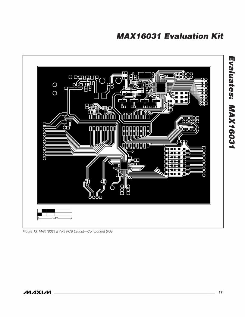
Figure 13. MAX16031 EV Kit PCB Layout—Component Side

Eva
lua
tes:
M
AX
16
03
1
MAX16031 Evaluation Kit
Maxim cannot assume responsibility for use of any circuitry other than circuitry entirely embodied in a Maxim product. No circuit patent licenses areimplied. Maxim reserves the right to change the circuitry and specifications without notice at any time.
18 ____________________Maxim Integrated Products, 120 San Gabriel Drive, Sunnyvale, CA 94086 408-737-7600
© 2007 Maxim Integrated Products is a registered trademark of Maxim Integrated Products, Inc.
Figure 14. MAX16031 EV Kit PCB Layout—Solder Side