max17a lowpower ultrasall dal driver iolin device … ldo 5v reg v33 v5 v24 control and monitor uvlo...
TRANSCRIPT

General DescriptionThe MAX14827A integrates the high-voltage functions commonly found in industrial sensors, including drivers and regulators. The MAX14827A features two ultra low-power drivers with active reverse-polarity protection. Operation is specified for normal 24V supply voltages up to 60V. Transient protection is simplified due to high voltage tolerance allowing the use of micro TVS. The device features a flexible control interface. Pin-control logic inputs allow for operation with switching sensors that do not use a microcontroller. For sensors that use a microcontroller, an SPI interface is available with extensive diagnostics. For IO-Link operation, a three-wire UART interface is provided, allowing interfacing to the microcontroller UART. Finally, a multiplexed UART/SPI option allows using one serial microcontroller interface for shared SPI and UART interfaces.The device includes on-board 3.3V and 5V linear regulators for low-noise analog/logic supply rails. The MAX14827A is available in a (4mm x 4mm) 24-pin TQFN package and a (2.5mm x 2.5mm) 25-pin wafer-level package (WLP) and is specified over the extended -40°C to +125°C temperature range.
Applications Industrial sensors IO-Link sensors and actuators Safety applications
Benefits and Features Low Power Dissipation for Small Sensors
• 2.3Ω/2.7Ω (typ) Driver On-Resistance• 70mW (typ) Power Dissipation at 100mA (When
Both C/Q and DO Drivers Are Driving) High Configurability and Integration Reduce SKUs
• Auxiliary 24V Digital Output and Input• Selectable Driver Current: 50mA to 250mA• SPI/Pin-Control Interface for Configuration and
Monitoring• Multiplexed SPI/UART Interface Option• 5V and 3.3V Linear Regulators• Optional External Transistor Supports Higher
Regulator Load Capability• Integrated LED Driver
Selectable Driver Integrated Protection Enables Robust Communication• 65V Absolute Maximum Ratings on Interface and
Supply Pins Allows for Flexible TVS Protection• 9V to 60V Specified Operation • Glitch Filters for Improved Burst Resilience and
Noise• Thermal Shutdown Auto-Retry Cycling• Hot-Plug Supply Protection • Reverse Polarity Protection of All Sensor Interface
Inputs/Outputs• -40°C to +125°C Operating Temperature Range
Ordering Information appears at end of data sheet.
IO-Link is a registered trademark of Profibus User Organization (PNO).SPI is a trademark of Motorola, Inc.
19-8592; Rev 1; 9/16
MAX14827A
GND
C/Q
DO
V24REGV5
L+
L-
1
43
2
DI
1µF
MICROCONTROLLER
VCC
3.3V
5V
VL V33
GPIO IRQ/OC
10kΩ
SPI
RX RX
IRQ WU
TX TX
RTS TXEN
GND
SPI/PIN
1µF
UARTSEL
C/Q
DI/DO
0.1µF
GPO LED1IN
LED1
MAX14827A Low-Power, Ultra-Small, Dual Driver, IO-Link Device Transceiver
Typical Operating Circuit
EVALUATION KIT AVAILABLE

3.3V LDO 5V REG
V33 V24V5
CONTROL AND
MONITOR
UVLO
VL
MAX14827A
LED DRIVER
LED2*LED1
LED1IN
REG
REV POL PROTECTIONSPI/PIN
IRQ/OCCS/PP
SDI/TX/NPNCLK/TXEN/200MA
SDO/RX/THSH
RX
TX
TXENUARTSEL
Transceiver C/Q
WAKE-UP DETECTWU
DOLO
LI DI
GND
* WLP PACKAGE ONLY
VDRV
DRIVER
VDRV
PROTECTION
PROTECTION
MAX14827A Low-Power, Ultra-Small, Dual Driver, IO-Link Device Transceiver
www.maximintegrated.com Maxim Integrated 2
Functional Diagram

(All voltages referenced to GND, unless otherwise noted.)V24 .........................................................................-70V to +65VREG ..............................................................-0.3V to (V5 + 16V)V5, VL ......................................................................-0.3V to +6VV33 ..............................................................-0.3V to (V5 + 0.3V)C/Q, DO, DI .................. MIN: Larger of -70V and (V24 - 70V) to MAX: the lower of +70V and (V24 + 70V)Logic Inputs: CS/PP, TXEN, TX, LED1IN, LI, UARTSEL, CLK/TXEN/200MA, SPI/PIN, SDI/TX/NPN ..............................................-0.3V to (VL + 0.3V)Logic Outputs: RX, LI, LO WU, SDO/RX/THSH ................ -0.3V to (VL + 0.3V) IRQ/OC ..................................................................-0.3V to +6VLED1, LED2 .................................................. -0.3V to (V5+0.3V)
Continuous Current Into GND and V24 ................................±1AContinuous Current Into C/Q and DO ............................±500mA Continuous Current Into V5 and REG ............................±100mAContinuous Current Into Any Other Pin ............................±50mAContinuous Power Dissipation
TQFN (derate 27.8mW/°C above +70°C)..................2222mW WLP (derate 22.7mW/°C above +70°C) ....................1816mWOperating Temperature Range ......................... -40°C to +125°CMaximum Junction Temperature ......................Internally LimitedStorage Temperature Range ............................ -65°C to +150°CSoldering Temperature (reflow, TQFN and WLP) ...........+260°C
TQFN Junction-to-Ambient Thermal Resistance (θJA) ..........36°C/W Junction-to-Case Thermal Resistance (θJC) .................3°C/W
WLP Junction-to-Ambient Thermal Resistance (θJA) ..........44°C/W
(Note 1)
(V24 = 9V to 60V, V5 = 4.5V to 5.5V, VL = 2.5V to 5.5V, VGND = 0V; REG unconnected, all logic inputs at VL or GND; TA = -40°C to +125°C, unless otherwise noted. Typical values are at V24 = 24V, V5 = 5V, VL = 3.3V, and TA = +25°C, unless otherwise noted.) (Note 2)
PARAMETER SYMBOL CONDITIONS MIN TYP MAX UNITSV24 Supply Voltage V24 9 60 V
V24 Undervoltage-Lockout Threshold V24UVLO
V24 rising 6 7.8 9V
V24 falling 6 7.2 9V24 Undervoltage-Lockout-Threshold Hysteresis V24UVLO_HYST 570 mV
V24 Supply Current I24
V5 powered externally, REG is unconnected
C/Q and DO disabled (CQ_Dis = 1, DO_Dis = 1)
0.14 0.5
mA
C/Q and DO in push-pull configuration, CL[10] = 11, C/Q and DO high, no load on C/Q or DO
1.1 1.75
C/Q and DO in push-pull configuration, CL[10] = 11, C/Q and DO low, no load on C/Q or DO
1.4 1.8
V24 Low-Voltage Warning Threshold V24W 14.5 16.5 18 V
MAX14827A Low-Power, Ultra-Small, Dual Driver, IO-Link Device Transceiver
www.maximintegrated.com Maxim Integrated 3
Note 1: Package thermal resistances were obtained using the method described in JEDEC specification JESD51-7, using a four-layer board. For detailed information on package thermal considerations, refer to www.maximintegrated.com/thermal-tutorial.
Absolute Maximum Ratings
Stresses beyond those listed under “Absolute Maximum Ratings” may cause permanent damage to the device. These are stress ratings only, and functional operation of the device at these or any other conditions beyond those indicated in the operational sections of the specifications is not implied. Exposure to absolute maximum rating conditions for extended periods may affect device reliability.
Package Thermal Characteristics
DC Electrical Characteristics

(V24 = 9V to 60V, V5 = 4.5V to 5.5V, VL = 2.5V to 5.5V, VGND = 0V; REG unconnected, all logic inputs at VL or GND; TA = -40°C to +125°C, unless otherwise noted. Typical values are at V24 = 24V, V5 = 5V, VL = 3.3V, and TA = +25°C, unless otherwise noted.) (Note 2)
PARAMETER SYMBOL CONDITIONS MIN TYP MAX UNITSV5 Supply Voltage 4.5 5.5 VV5 Undervoltage-Lockout Threshold V5UVLO
V5 rising 2.8 3.5 4.5V
V5 falling 2.8 3.45 4.5
V5 Supply Current I5_IN
External 5V applied to V5, REG is unconnected, no load on LED1 or LED2
C/Q and DO disabled (CQ_Dis = 1, DO_Dis = 1), V33 disabled (V33_Dis = 1)
0.64 0.9
mA
C/Q and DO in push-pull configuration, CL[10] = 11, C/Q and DO high, V33 enabled, no load on C/Q, DO, or V33
1.37 1.75
C/Q and DO in push-pull configuration, CL[10] = 11, C/Q and DO low, V33 enabled, no load on C/Q, DO, or V33
1.41 1.8
VL Logic-Level Supply Voltage VL 2.5 5.5 V
VL Undervoltage Threshold VLUVLO 0.9 1.7 2.4 V
VL Logic-Level Supply Current ILAll logic inputs at VL or GND, all logic outputs unconnected 0.25 3 µA
5V LINEAR REGULATOR/CONTROLLER (V5)
V5 Output Voltage V5REG = V5, no load on V5, 9V ≤ V24 ≤ 60V 4.75 5.00 5.25 V
Load Regulation ΔV5_LDRREG = V5, 0mA < ILOAD < 30mA, V24 = 24V 0.02 0.2 %
Line Regulation ΔV5_LNRREG = V5, ILOAD = 1mA, V24 from 9V to 60V 0.01 4 mV/V
REG Output Current IREG Internal regulator or external NPN 30 mA
V24 REG Dropout Voltage ΔVREG V24 = 9V, V5 = 4.5V, IREG = 5mA 2.35 V
REG Open Voltage VREG_OPN V24 = 60V, V5 = 4.5V, no load on REG 10 13 16 V
V5 Capacitance CV5Allowed capacitance on V5, REG connected to V5 (Note 3) 0.8 1 2 µF
MAX14827A Low-Power, Ultra-Small, Dual Driver, IO-Link Device Transceiver
www.maximintegrated.com Maxim Integrated 4
DC Electrical Characteristics (continued)

(V24 = 9V to 60V, V5 = 4.5V to 5.5V, VL = 2.5V to 5.5V, VGND = 0V; REG unconnected, all logic inputs at VL or GND; TA = -40°C to +125°C, unless otherwise noted. Typical values are at V24 = 24V, V5 = 5V, VL = 3.3V, and TA = +25°C, unless otherwise noted.) (Note 2)
PARAMETER SYMBOL CONDITIONS MIN TYP MAX UNITS3.3V LINEAR REGULATOR (V33)V33 Output Voltage V33 No load on V33 3.1 3.3 3.5 V
V33 Load Regulation V33_LDR 0mA < ILOAD < 30mA 0 0.4 0.8 %
V33 Capacitance CV33Allowed capacitance on V33, V33 enabled (Note 3) 0.8 1 µF
C/Q, DO DRIVER
Driver On-Resistance ROH
High-side enabled, V24 = 24V, CL[10] = 11, ILOAD = -200mA (Note 3) 2.65 4.6
ΩROL
Low-side enabled, V24 = 24V, CL[10] = 11, ILOAD = +200mA (Note 3) 2.3 4.45
Driver Current Limit ICL
SPI/PIN = high, VDRIVER = (V24 – 3V) or 3V, CL_Dis = 0
CL[10] = 00 50 65 80
mA
CL[10] = 01 100 120 150
CL[10] = 10 200 230 275
CL[10] = 11 250 290 350
SPI/PIN = low, VDRIVER = (V24 – 3V) or 3V
CLK/TXEN/ 200MA = low 100 120 150
CLK/TXEN/ 200MA = high 200 230 275
Driver Peak Current ICL_PEAK DC current 490 mA
C/Q Leakage Current ILEAK_CQ
C/Q driver is disabled (C/Q_Dis = 1), RX disabled (Rx_Dis = 1), V24 = 24V, (V24 - 65V) ≤ VC/Q ≤ +60V
-70 +10
µA
C/Q driver enabled
NPN mode, set to high impedance (TX = low), VC/Q = 24V
17.4
PNP mode, set to high impedance (TX = high) VC/Q = 0V
0
PNP mode, set to high impedance (TX = 0) VC/Q = 24V
22.9
PNP mode, set to high impedance (TX = 0) VC/Q = 0V
-43.5
MAX14827A Low-Power, Ultra-Small, Dual Driver, IO-Link Device Transceiver
www.maximintegrated.com Maxim Integrated 5
DC Electrical Characteristics (continued)

(V24 = 9V to 60V, V5 = 4.5V to 5.5V, VL = 2.5V to 5.5V, VGND = 0V; REG unconnected, all logic inputs at VL or GND; TA = -40°C to +125°C, unless otherwise noted. Typical values are at V24 = 24V, V5 = 5V, VL = 3.3V, and TA = +25°C, unless otherwise noted.) (Note 2)
PARAMETER SYMBOL CONDITIONS MIN TYP MAX UNITS
DO Leakage Current ILEAK_DO
DO driver is disabled (DO_Dis =1), V24 = 24V, (V24 -65V) ≤ VDO ≤ +60V -10 +10
µADO driver enabled
NPN mode, set to high impedance (LO = low) , VDO = 24V
6.0
PNP mode, set to high impedance (LO = high) VDO = 0V
0
PNP mode, set to high impedance (CQDOPAR = 1, TXEN = 0), VDO = 24V
11.6
PNP mode, set to high impedance (CQDOPAR = 1, TXEN = 0), VDO = 0V
-42.4
C/Q Output Reverse Current IREV_CQ
C/Q driver enabled and in push-pull configuration, V24 = 30V, VC/Q = (V24 + 5V) or (VGND - 5V)
-60 +1000 μA
DO Output Reverse Current IREV_DO
DO driver enabled and in push-pull configuration, V24 = 30V, VDO = (V24 + 5V) or (VGND - 5V)
-60 +1000 μA
Weak Pulldown Current IPD
SPI/PIN = high, driver disabled (CQ_Dis = 1, DO_Dis =1)
VDRIVER = 5V,CQ_WPD = 1, DO_WPD = 1, CQ_WPU = 0, DO_WPU = 0
200 300 400
μAVDRIVER = 24V,CQ_WPD = 1, DO_WPD = 1, CQ_WPU = 0, DO_WPU = 0
200 470 1000
Weak Pullup Current IPU
SPI/PIN = high, driver disabled (CQ_Dis = 1, DO_Dis = 1), VDRIVER = V24 - 5V
CQ_WPU = 1, DO_WPU = 1, CQ_WPD = 0, DO_WPD = 0,
-400 -300 -200 μA
C/Q, DI RECEIVER
Input Voltage Range VIN For valid RX/LI logic V24 – 65 +65 V
C/Q, DI Input Threshold High VTH C/Q driver disabledV24 > 18V 11 11.8 12.5 V
V24 < 18V 59 65.5 72 % of V24
C/Q, DI Input Threshold Low VTL C/Q driver disabledV24 > 18V 9 9.8 10.5 V
V24 < 18V 45 54.5 63 % of V24
MAX14827A Low-Power, Ultra-Small, Dual Driver, IO-Link Device Transceiver
www.maximintegrated.com Maxim Integrated 6
DC Electrical Characteristics (continued)

(V24 = 9V to 60V, V5 = 4.5V to 5.5V, VL = 2.5V to 5.5V, VGND = 0V; REG unconnected, all logic inputs at VL or GND; TA = -40°C to +125°C, unless otherwise noted. Typical values are at V24 = 24V, V5 = 5V, VL = 3.3V, and TA = +25°C, unless otherwise noted.) (Note 2)
PARAMETER SYMBOL CONDITIONS MIN TYP MAX UNITS
C/Q, DI Input Hysteresis VHYS_CQ C/Q driver disabledV24 > 18V 2 V
V24 < 18V 11 % of V24
C/Q Input Capacitance CIN_CQDriver disabled, weak pull-up and pull-down disabled, f = 100kHz 50 pF
DI Input Capacitance CIN_DI f = 100kHz 10 pF
C/Q Input Current IIN_CQ
C/Q driver disabled (CQ_Dis = 1), C/Q receiver enabled, V24 = 24V
-5V ≤ VC/Q ≤ (V24 + 5V) -10 +30
µA(V24 - 65V)≤ VC/Q ≤ +60V -70 +70
DI Leakage Current ILEAK_DIDI receiver disabled (DI_Dis = 1), V24 = 24V, (V24 - 65V) ≤ VDI ≤ +60V -40 +150 µA
DI Input Current IIN_DIDI receiver enabled, V24 = 24V
-5V ≤ VDI ≤ (V24 + 5V) -10 +35µA(V24 - 65V) ≤ VDI ≤
+60V -40 +200
LOGIC INPUTS (CS/PP, TXEN, TX, LO, LED1IN, CLK/TXEN/200MA, SPI/PIN, SDI/TX/NPN)Logic Input Voltage Low VIL 0.2 x VL V
Logic Input Voltage High VIH 0.8 x VL V
Logic Input Leakage Current ILEAK Logic input = GND or VL -1 +1 µA
LOGIC OUTPUTS (RX, LI, WU, IRQ/OC, SDO/RX/THSH)Logic Output Voltage Low VOL IOUT = -5mA 0.4 V
Logic Output Voltage High VOH IOUT = 5mA VL - 0.4 V
IRQ/OC Open-Drain Leakage Current ILK_OD
IRQ/OC high impedance, IRQ/OC = GND or VL -1 +1 μA
SDO Leakage Current ILK_SDOSPI/PIN = high, CS/PP = high, SDO/RX/THSH = GND or VL -1 +1 µA
RX, LI Leakage Current ILK_RXLISPI/PIN = high, DI_Dis = 1, RX_Dis = 1, RX/LI = GND or VL -1 +1 µA
LED DRIVERS (LED1, LED2)LED Output Voltage Low VLEDOL IOUT = -5mA 0.4 V
LED Output Voltage High VLEDOH IOUT = 10mA V5 – 0.4 V
THERMAL MANAGEMENT
Thermal Warning Threshold TWRNDie junction temperature rising, TempW and TempWInt bits are set +140 °C
Thermal Warning Threshold Hysteresis TWRN_HYS
Die junction temperature falling, TempW bit cleared 15 °C
Per-Driver Thermal Shutdown Temperature TSHUT_D
Driver temperature rising, temperature at which the driver is turned off +160 °C
MAX14827A Low-Power, Ultra-Small, Dual Driver, IO-Link Device Transceiver
www.maximintegrated.com Maxim Integrated 7
DC Electrical Characteristics (continued)
PARAMETER SYMBOL CONDITIONS MIN TYP MAX UNITS
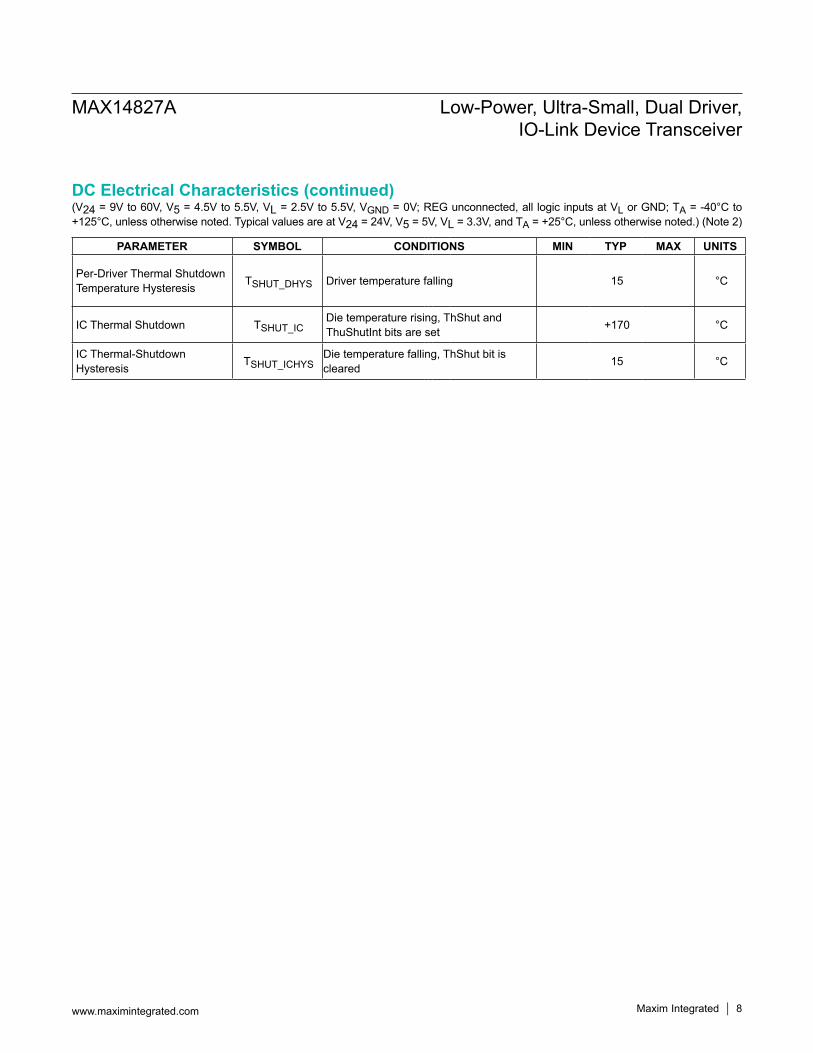
Per-Driver Thermal Shutdown Temperature Hysteresis TSHUT_DHYS Driver temperature falling 15 °C
IC Thermal Shutdown TSHUT_ICDie temperature rising, ThShut and ThuShutInt bits are set +170 °C
IC Thermal-Shutdown Hysteresis TSHUT_ICHYS
Die temperature falling, ThShut bit is cleared 15 °C
MAX14827A Low-Power, Ultra-Small, Dual Driver, IO-Link Device Transceiver
www.maximintegrated.com Maxim Integrated 8
(V24 = 9V to 60V, V5 = 4.5V to 5.5V, VL = 2.5V to 5.5V, VGND = 0V; REG unconnected, all logic inputs at VL or GND; TA = -40°C to +125°C, unless otherwise noted. Typical values are at V24 = 24V, V5 = 5V, VL = 3.3V, and TA = +25°C, unless otherwise noted.) (Note 2)
DC Electrical Characteristics (continued)

(V24 = 18V to 30V, V5 = 4.5V to 5.5V, VL = 2.5V to 5.5V, VGND = 0V; REG unconnected, all logic inputs at VL or GND; TA = -40°C to +125°C, unless otherwise noted. Typical values are at V24 = 24V, V5 = 5V, VL = 3.3V, and TA = +25°C, unless otherwise noted.) (Note 2)
PARAMETER SYMBOL CONDITIONS MIN TYP MAX UNITSC/Q, DO DRIVER
Driver Low-to-High Propagation Delay tPDLH_PP
Push-pull and PNP configuration, Figure1 0.16 0.4μs
NPN configuration, Figure 1 0.16
Driver High-to-Low Propagation Delay tPDHL_PP
Push-pull and NPN configuration, Figure1 0.28 0.4μs
PNP configuration, Figure 1 0.28
Driver Skew tSKEWPush-pull configuration, Figure 1| tPDLH - tPDHL | -0.3 +0.3 μs
Driver Rise Time tRISE Push-pull and PNP configuration, Figure 1 0.12 0.4 μs
Driver Fall Time tFALL Push-pull and NPN configuration, Figure 1 0.12 0.4 µs
Driver Enable Time High tENHPush-pull and PNP configuration, CQDOPar = 1 for DO, Figure 2 0.15 0.4 µs
Driver Enable Time Low tENLPush-pull and NPN configuration, CQDOPar = 1 for DO, Figure 3 0.27 0.4 µs
Driver Disable Time High tDISHPush-pull and PNP configuration, CQDOPar = 1 for DO, Figure 2 1.8 3 µs
Driver Disable Time Low tDISLPush-pull and NPN configuration, CQDOPar = 1 for DO, Figure 3 1.5 3 µs
C/Q, DI RECEIVER (Figure 4)
C/Q Receiver Low-to-High Propagation Delay tPRLH_CQ
SPI/PIN = high or low, CQFil = 0 0.85 1.3 2.1µs
SPI/PIN = high, CQFil = 1 0.2 0.3 0.5
C/Q Receiver High-to-Low Propagation Delay tPRHL_CQ
SPI/PIN = high or low, CQFil = 0 0.85 1.3 2.1µs
SPI/PIN = high, CQFil = 1 0.2 0.3 0.5DI Receiver Low-to-High Propagation Delay tPRLH_DI 1.3 2.2 3.5 µs
DI Receiver High-to-Low Propagation Delay tPRHL_DI 1.3 2.2 3.5 µs
DRIVER CURRENT LIMITING
Blanking Time tCL_ARBLSPI/PIN = high
CL_BL[10] = 00 0.128
ms
CL_BL[10] = 01 0.5
CL_BL[10] = 10 1
CL_BL[10] = 11 5
SPI/PIN = low 0.128
MAX14827A Low-Power, Ultra-Small, Dual Driver, IO-Link Device Transceiver
www.maximintegrated.com Maxim Integrated 9
AC Electrical Characteristics

(V24 = 18V to 30V, V5 = 4.5V to 5.5V, VL = 2.5V to 5.5V, VGND = 0V; REG unconnected, all logic inputs at VL or GND; TA = -40°C to +125°C, unless otherwise noted. Typical values are at V24 = 24V, V5 = 5V, VL = 3.3V, and TA = +25°C, unless otherwise noted.) (Note 2)
Note 2: All devices are 100% production tested at TA = +25°C. Limits over the operating temperature range are guaranteed by design.
Note 3: Not production tested. Guaranteed by design.Note 4: Autoretry functionality is not available in pin-mode.
PARAMETER SYMBOL CONDITIONS MIN TYP MAX UNITS
Autoretry Period tCL_ARPSPI/PIN = high, ArEn = 1 (Note 4)
TAr[10] = 00 50
msTAr[10] = 01 100
TAr[10] = 10 200
TAr[10] = 11 500
WAKE-UP DETECTION (Figure 5)Wake-Up Input Minimum Pulse Width tWUMIN CL = 3nF 55 66 75 µs
Wake-Up Input Maximum Pulse Width tWUMAX 85 95 110 µs
WU Output Low Time tWUL Valid wake-up condition on C/Q 100 200 300 µs
SPI TIMING (CS/PP, CLK/TXEN/200MA,SDI,TX/NPN, SDO/RX/THSH) (Figure 6)Maximum SPI Clock Frequency 12.5 MHz
CLK/TXEN/200MA Clock Period tCH+CL 80 ns
CLK/TXEN/200MA Pulse-Width High tCH 40 ns
CLK/TXEN/200MA Pulse-Width Low tCL 40 ns
CS/PP Fall to CLK/TXEN/200MA Rise Time tCSS 20 ns
CLK/TXEN/200MA Rise to CS/PP Rise Hold Time tCSH 40 ns
SDI/TX/NPN Hold Time tDH 10 ns
SDI/TX/NPN Setup Time tDS 25 ns
Output Data Propagation Delay tDO 20 nsSDO/RX/THSH Rise and Fall Times tFT 20 ns
Minimum CS/PP Pulse tCSW 10 ns
MAX14827A Low-Power, Ultra-Small, Dual Driver, IO-Link Device Transceiver
www.maximintegrated.com Maxim Integrated 10
AC Electrical Characteristics (continued)

Figure 1. C/Q and LO Driver Propagation Delays and Rise/Fall Times
Figure 2. C/Q Driver Enable Low and Disable High Timing with External Pullup Resistor
TX, LO
C/Q, DO
tPDHL
tFALL
90%
10%50%
TXEN
0V
VL
0V
VL
0V
V2490%
10%50%
tRISE
tPDLH
50% 50%
TX, LO
GND
C/Q, DO
TXEN
MAX14827A
5kΩ3.3nF
TX, LO
GND
C/Q, DO
TXEN
MAX14827A
5kΩ
3.3nF
V24
PUSH-PULL AND PNP MODE NPN MODE
TXEN
C/Q
tENL
10%50%
TXEN
GND
TX
VL
VL
0V
V24
0V
5kΩ
3.3nF
V24
MAX14827A
tDISH
C/Q
MAX14827A Low-Power, Ultra-Small, Dual Driver, IO-Link Device Transceiver
www.maximintegrated.com Maxim Integrated 11

Figure 3. C/Q Driver Enable High and Disable Low Timing
Figure 4. C/Q and DI Receiver Propagation Delays
TXEN
C/Q
tENH
90%50%
TXEN
GND
TX
VL
0V
V24
0V
5kΩ3.3nF
MAX14827A
tDISL
C/Q
C/Q, DI
RX, LI
tPRLH
tPRHL
50%
50%
V24
0V
VL
0V
C/Q, DIGND
RX, LI
TXEN
15pF
MAX14827A
50%
50%
MAX14827A Low-Power, Ultra-Small, Dual Driver, IO-Link Device Transceiver
www.maximintegrated.com Maxim Integrated 12

Figure 5. Wake-Up Detection Timing
Figure 6. SPI Timing Diagram
TXEN
GND
TXEN
TX
WU
tWUMIN < tWU < tWUMAX
TX
WU
tWUL
< tWUMINNO WAKE-UP
C/Q
C/Q
MAX14827A
tCSH tCLtCSS tCH tCSH
CS/PP
CLK/TXEN/200MA
SDI/TX/NPN
SDO/RX/THSH
tDStDH
tDO
MAX14827A Low-Power, Ultra-Small, Dual Driver, IO-Link Device Transceiver
www.maximintegrated.com Maxim Integrated 13

(V24 = 24V, VL = V33, REG is shorted to V5, C/Q and DO in push-pull configuration, TA = +25°C, unless otherwise noted.)
0
1
2
3
4
5
6
7
8
9
10
0 50 100 150 200 250I24
SUP
PLY
CURR
ENT
(mA)
C/Q SWITCHING RATE (kbps)
I24 SUPPLY CURRENTvs. C/Q SWITCHING RATE
toc02
C/Q IN PUSH-PULLDO DISABLED
NO LOAD
1nF LOAD
0.00
0.25
0.50
0.75
1.00
1.25
1.50
0 50 100 150 200 250
I24 S
UPPL
Y CU
RREN
T (m
A)
C/Q SWITCHING RATE (kbps)
V5 SUPPLY CURRENTvs. C/Q SWITCHING RATE
toc03
C/Q IN PUSH-PULLDO DISABLED
REG UNCONNECTEDV5 = 5V
NO LOAD
1nF LOAD
23.0
23.1
23.2
23.3
23.4
23.5
23.6
23.7
23.8
23.9
24.0
0 25 50 75 100 125 150 175 200 225 250
OUTP
UT V
OLTA
GE H
IGH
(V)
LOAD CURRENT (mA)
C/Q DRIVER OUTPUT HIGHvs. LOAD CURRENT
toc04
TA = -40ºC
TA = +25ºC
TA = +125ºC
C/Q HIGH-SIDE ENABLED
0.0
0.1
0.2
0.3
0.4
0.5
0.6
0.7
0.8
0.9
1.0
0 25 50 75 100 125 150 175 200 225 250
OUTP
UT V
OLTA
GE LO
W (V
)
LOAD CURRENT (mA)
C/Q DRIVER OUTPUT LOWvs. SINK CURRENT
toc05
TA = -40ºC
TA = +25ºC
TA = +125ºC
C/Q LOW-SIDE ENABLED
0.0
0.5
1.0
1.5
2.0
2.5
3.0
6 12 18 24 30 36 42 48 54 60
SUPP
LY C
URRE
NT (m
A)
SUPPLY VOLTAGE (V)
I24 SUPPLY CURRENT vs. V24 SUPPLY VOLTAGE
toc01
C/Q AND DO ARE PUSH-PULLNO SWITCHING: C/Q = HIGH, DO = LOW
TA = -40ºCTA = +25ºC
TA = +125ºC
23.0
23.1
23.2
23.3
23.4
23.5
23.6
23.7
23.8
23.9
24.0
0 25 50 75 100 125 150 175 200 225 250
OUTP
UT V
OLTA
GE H
IGH
(V)
LOAD CURRENT (mA)
DO DRIVER OUTPUT HIGHvs. LOAD CURRENT
toc06
TA = -40ºC
TA = +25ºC
TA = +125ºC
DO HIGH-SIDE ENABLED
MAX14827A Low-Power, Ultra-Small, Dual Driver, IO-Link Device Transceiver
Maxim Integrated 14www.maximintegrated.com
Typical Operating Characteristics

(V24 = 24V, VL = V33, REG is shorted to V5, C/Q and DO in push-pull configuration, TA = +25°C, unless otherwise noted.)
0.00
0.10
0.20
0.30
0.40
0.50
0.60
0.70
0.80
0.90
1.00
0 25 50 75 100 125 150 175 200 225 250
OUTP
UT V
OLTA
GE LO
W (V
)
LOAD CURRENT (mA)
DO DRIVER OUTPUT LOWvs. SINK CURRENT
toc07
TA = -40ºC
TA = +25ºC
TA = +125ºC
DO HIGH-SIDE ENABLED
0
50
100
150
200
250
300
350
0 6 12 18 24 30
SINK
CUR
RENT
(mA)
OUTPUT VOLTAGE LOW (V)
C/Q CURRENT LIMIT toc08
CL[10] = 11
CL[10] = 10
CL[10] = 00
CL[10] = 01
C/Q IN PUSH-PULLC/Q IS LOW
-350
-300
-250
-200
-150
-100
-50
0
0 6 12 18 24 30
SOUR
CE C
URRE
NT (m
A)
OUTPUT VOLTAGE LOW (V)
C/Q CURRENT LIMIT toc09
CL[10] = 11
CL[10] = 10
CL[10] = 00
CL[10] = 01
C/Q IN PUSH-PULLC/Q IS HIGH -60
-50
-40
-30
-20
-10
0
10
-10 0 10 20 30 40 50 60
LEAK
AGE
CURR
ENT
(µA)
C/Q VOLTAGE (V)
C/Q DRIVER LEAKAGE CURRENTvs. C/Q VOLTAGE
toc10
TA = -40ºC
TA = +125ºC
TA = +25ºC
C/Q driver disabled
-10
-8
-6
-4
-2
0
2
4
6
8
10
-10 0 10 20 30 40 50 60
LEAK
AGE
CURR
ENT
(µA)
DO VOLTAGE (V)
DO DRIVER LEAKAGE CURRENTvs. DO VOLTAGE
toc11
TA = +125ºC
TA = -40ºC and +25ºC
DO driver disabled-200
-100
0
100
200
300
400
500
600
700
800
900
-10 0 10 20 30 40 50 60
PULL
-DOW
N CU
RREN
T (µ
A)
C/Q VOLTAGE (V)
C/Q WEAK PULL-DOWN CURRENTvs. C/Q VOLTAGE
toc12
TA = -40ºC
TA = +25ºC
TA = +125ºC
CQ_Dis = 1CQ_WPD = 1
MAX14827A Low-Power, Ultra-Small, Dual Driver, IO-Link Device Transceiver
Maxim Integrated 15www.maximintegrated.com
Typical Operating Characteristics (continued)

(V24 = 24V, VL = V33, REG is shorted to V5, C/Q and DO in push-pull configuration, TA = +25°C, unless otherwise noted.)
-500
-400
-300
-200
-100
0
100
200
300
400
500
-10 0 10 20 30 40 50 60
PULL
-UP
CURR
ENT
(mA)
C/Q VOLTAGE (V)
C/Q WEAK PULL-UP CURRENTvs. C/Q VOLTAGE
toc13
TA = +25ºC
TA = +125ºC
TA = -40ºC
CQ_Dis = 1CQ_WPU = 1
-20
-10
0
10
20
30
40
50
-10 0 10 20 30 40 50 60
INPU
T CU
RREN
T (µ
A)INPUT VOLTAGE (V)
C/Q RECEIVER INPUT CURRENT vs. INPUT VOLTAGE
toc14
TA = -40ºC
TA = +125ºC
TA = +25ºC
C/Q receiver enabled
-10
0
10
20
30
40
50
60
70
-10 0 10 20 30 40 50 60
INPU
T CU
RREN
T (µ
A)
INPUT VOLTAGE (V)
DI RECEIVER INPUT CURRENT vs. INPUT VOLTAGE
toc15
TA = -40ºC
TA = +125ºC
TA = +25ºC
C/Q DRIVER SWITCHING INTO 1nF LOAD
TX2V/div0V
C/Q5V/div
0V
toc16
10µs/div
VOUTN
VINSIDE
VBACKUP
C/Q IS PUSH-PULLCLOAD = 1nF
C/Q DRIVER SWITCHING INTO 4.7nF LOAD
TX2V/div0V
C/Q5V/div
0V
toc17
10µs/div
WAKE-UP DETECTION
C/Q10V/div
0V
WU2V/div
0V
toc18
40µs/div
VOUTN
VINSIDE
VBACKUP
TXEN = VLTX = GND
MAX14827A Low-Power, Ultra-Small, Dual Driver, IO-Link Device Transceiver
Maxim Integrated 16www.maximintegrated.com
Typical Operating Characteristics (continued)

(V24 = 24V, VL = V33, REG is shorted to V5, C/Q and DO in push-pull configuration, TA = +25°C, unless otherwise noted.)
-0.100
-0.090
-0.080
-0.070
-0.060
-0.050
-0.040
-0.030
-0.020
-0.010
0.000
0 5 10 15 20 25 30
LOAD
REG
UIAT
ION
(%)
LOAD CURRENT (mA)
V5 LINEAR REGULATOR LOAD REGULATION
toc19
TA = -40ºC
TA = +25ºC TA = +125ºC
5.040
5.042
5.044
5.046
5.048
5.050
5.052
5.054
5.056
5.058
5.060
10 20 30 40 50 60V5
VOL
TAGE
(V)
V24 VOLTAGE (V)
V5 LINEAR REGULATOR LINE REGULATION
toc20
EXTERNAL NPN TRANSISTOR CONNECTED TO V5 AND REG
ILOAD = 10mA ON V5
-0.9
-0.8
-0.7
-0.6
-0.5
-0.4
-0.3
-0.2
-0.1
0.0
0 5 10 15 20 25 30
LOAD
REG
UIAT
ION
(%)
LOAD CURRENT (mA)
V33 LINEAR REGULATOR LOAD REGULATION
toc21
TA = -40ºC
TA = +25ºC
TA = +125ºC
0.0
0.5
1.0
1.5
2.0
2.5
3.0
3.5
4.0
4.5
5.0
5.5
0 2 4 6 8 10 12 14 16 18 20
LED1
OR
LED2
VOL
TAGE
(V)
LOAD CURRENT (mA)
LED DRIVER OUTPUT HIGHVOLTAGE vs LOAD CURRENT
toc22
0
20
40
60
80
100
120
140
160
180
200
0 2 4 6 8 10 12 14 16 18 20
LED1
OR
LED2
VOL
TAGE
(mV)
LOAD CURRENT (mA)
LED DRIVER OUTPUT LOWVOLTAGE vs SINK CURRENT
toc23
LED DRIVER TURNED OFF
5.00
5.01
5.02
5.03
5.04
5.05
5.06
5.07
5.08
5.09
5.10
-45 -20 5 30 55 80 105 130
V5 V
OLTA
GE (V
)
TEMPERATURE (ºC)
V5 VOLTAGE vs TEMPERATURE
ILOAD = 20mA
toc24
MAX14827A Low-Power, Ultra-Small, Dual Driver, IO-Link Device Transceiver
Maxim Integrated 17www.maximintegrated.com
Typical Operating Characteristics

PIN
NAME PIN DESCRIPTION
FUNCTION
TQFN WLP
PARALLEL MODE
(SPI/PIN = High)
MULTIPLEXED MODE(SPI/PIN = High) PIN MODE
(SPI/PIN = Low)
UARTSEL = Low UARTSEL = high
1 E1 CS/PP CS/PP Logic Input
SPI active-low chip-select input. Drive CS/PP low to start the SPI read/write cycle. Drive CS/PP high to end the SPI cycle. UART interface is enabled on RX, TX, and TXEN.
SPI chip-select and UART signal select input. When CS/PP is high, the SPI interface is disabled and UART interface mode is enabled on the SDO/RX/THSH, SDI/TX/NPN, and CLK/TXEN/200MA logic pins.
Push-pull select input. Drive CS/PP high to enable push-pull mode for the C/Q and DO drivers. Drive CS/PP low to select PNP or NPN operation for the drivers.
2 D1 RX C/Q Receiver Logic Output
RX is the inverse logic of C/Q. RX can be disabled with the SPI interface. RX is high impedance when Rx_Dis = 1.
RX is the inverse logic of C/Q. RX is always active.
TOP VIEW(BUMP SIDE DOWN)
A
B
C
D
WLP2.5mm x 2.5mm
E
1+
V24C/Q DOGND DI
2 3 4 5
REGV5 V33LED1 VL
TXENTX UARTSELLED2 LI
SPI/PINRX WUSDO/RX/THSH LO
SDI/TX/NPNCS/PP IRQ/OCCLK/TXEN/
200MA LED1IN
CLK/TXEN/200MA
RX TX V5
REG
CS/P
P
LO LI VLWU
V33
SPI/PIN
SDI/TX/NPN
GND
V24
C/Q
LED1
TXEN
UART
SEL
SDO/RX/THSH
DOIRQ/OC
DILED1IN
TQFN4mm x 4mm
TOP VIEW
+
131415161718
12
11
10
9
8
7
19
20
21
22
23
24
654321
MAX14827A
* EP
MAX14827A Low-Power, Ultra-Small, Dual Driver, IO-Link Device Transceiver
www.maximintegrated.com Maxim Integrated 18
Pin Description
Pin Configuration

PIN
NAME PIN DESCRIPTION
FUNCTION
TQFN WLP
PARALLEL MODE
(SPI/PIN = High)
MULTIPLEXED MODE(SPI/PIN = High) PIN MODE
(SPI/PIN = Low)UARTSEL = Low UARTSEL = High
3 C2 TXENC/Q Driver
Enable Logic Input
Drive TXEN high to enable the C/Q driver. See Table 1.
With CS/PP low and ENMPX = 0, drive TXEN high to enable C/Q.
Drive TXEN high to enable the C/Q driver. Drive TXEN low to disable the C/Q driver and enable the C/Q receiver.
4 C1 TXC/Q Driver
Communication Input
The logic on the C/Q output is the inverse logic level of the signal on the TX input. See Table 1.
With CS/PP low and ENMPX = 0, the logic on the C/Q output is the inverse logic level of the signal on the SDI/TX/NPN input. Signals on TX are ignored. See the Mode Selection table.
The logic on the C/Q output is the inverse logic level of the signal on the TX input when TXEN is high.
5 B1 V55V Power-
Supply Input/Output
5V must be present on V5 for normal operation. Bypass V5 to GND with a 1μF capacitor. V5 can be supplied by the internal 5V linear regulator or by an external regulator. To use the internal regulator, connect V5 to REG, or to the emitter of an external NPN transistor. To bypass the internal regulator, connect an external 5V supply directly to V5.
6 B2 REG 5V Regulator Control Output
To use the internal linear regulator, connect REG to V5 or connect REG to the base of an external NPN pass transistor. Leave REG unconnected and connect V5 to an external 5V supply to bypass the internal regulator.
7 B3 LED1 LED Driver Output 1
LED1 is a 5V logic output. Connect a current-limiting resistor in series between LED1 and the LED to limit the LED current. LED1 can be controlled by driving the LED1IN high or low, of through the SPI interface. Set the LED1b bit high to turn on the LED, clear the LED1b bit to turn off the LED. Alternatively, drive the LED1IN input high to turn on the LED, drive LED1IN low to turn off the LED. See Table 2.
LED1 is a 5V logic output. Connect a current-limiting resistor in series between LED1 and the LED to limit the LED current. Drive the LED1IN input high to turn on the LED, drive LED1IN low to turn off the LED.
— C3 LED2 LED Driver Output 2
LED2 is a 5V logic output. Connect a current-limiting resistor in series between LED2 and the LED to limit the LED current. Set the LED2b bit high to turn on the LED, clear the LED2b bit to turn off the LED.
LED2 cannot be controlled in pin-mode. LED2 is off.
MAX14827A Low-Power, Ultra-Small, Dual Driver, IO-Link Device Transceiver
www.maximintegrated.com Maxim Integrated 19
Pin Description (continued)

PIN
NAME PIN DESCRIPTION
FUNCTION
TQFN WLP
PARALLEL MODE
(SPI/PIN = High)
MULTIPLEXED MODE(SPI/PIN = High) PIN MODE
(SPI/PIN = Low)UARTSEL = Low UARTSEL = high
8 A1 C/QC/Q Transceiver
Output/Input
The C/Q driver can be controlled and monitored with the logic input/output pins or through the SPI interface. Drive TXEN high to enable the C/Q driver. The logic on the C/Q output is the inverse logic-level of the signal in the TX input. RX is the logic inverse of C/Q.
Drive TXEN high to enable the C/Q driver. The logic on the C/Q output is the inverse logic-level of the signal in the TX input. RX is the logic inverse of C/Q.Configure the C/Q driver with the pin-mode inputs.
9 A2 V24 Power-Supply Input
Bypass V24 to GND with a 0.1μF ceramic capacitor as close to the device as possible.
10 A3 GND Ground
11 A4 DO DO Driver Output
DO is the inverse logic level of the LO input. The DO driver can be enabled/disabled, configured, controlled, and monitored with the logic input/output pins or through the SPI interface.
DO is the inverse logic level of the LO input. Configure the DO driver with the pin-mode inputs. DO cannot be disabled in pin-mode.
12 A5 DI DI Receiver Input
The DI receiver can be monitored on the LI output or through the SPI interface. The LI output is the inverse logic-level of the signal on the DI input.
The LI output is the inverse logic-level of the signal on the DI input. The DI receiver cannot be disabled in pin-mode.
13 B4 V333.3V Linear Regulator
Output
Bypass V33 to GND with a 1μF capacitor as close to the IC as possible. The V33 regulator can be disabled through the SPI interface.
Bypass V33 to GND with a 1μF capacitor as close to the IC as possible. V33 cannot be disabled in pin-mode.
14 B5 VL Logic-Level Supply Input
VL defines the logic levels on all of the logic inputs and outputs. Apply a voltage from 2.5V to 5.5V on VL. Bypass VL to GND with a 0.1μF ceramic capacitor.
15 C5 LI DI Receiver Logic Output
The LI output is the inverse logic-level of the signal on the DI input. Disable the LI output through the SPI interface. LI is high impedance when the DI_Dis bit is set.
The LI output is the inverse logic-level of the signal on the DI input. LI cannot be disabled in pin-mode.
MAX14827A Low-Power, Ultra-Small, Dual Driver, IO-Link Device Transceiver
www.maximintegrated.com Maxim Integrated 20
Pin Description (continued)
PIN
NAME PIN DESCRIPTION
FUNCTION
TQFN WLP
PARALLEL MODE
(SPI/PIN = High)
MULTIPLEXED MODE(SPI/PIN = High) PIN MODE
(SPI/PIN = Low)UARTSEL = Low UARTSEL = High
16 C4 UARTSELUART Interface
Select Logic Input
Drive UARTSEL low to use RX, TX, and TXEN for UART signaling.
When CS/PP is high, use SDO/RX/THSH, SDI/TX/NPN, and CLK/TXEN/200MA for UART signaling.
UARTSEL is inactive when SPI/PIN is low.
17 D5 LO DO Driver Logic Input
The logic on the DO output is the inverse logic-level of the signal on the LO input. Configure, control, and monitor the DO output through the logic pins or through the SPI interface.
The logic on the DO output is the inverse logic-level of the signal on the LO input. Configure the DO driver with the pin-mode inputs.
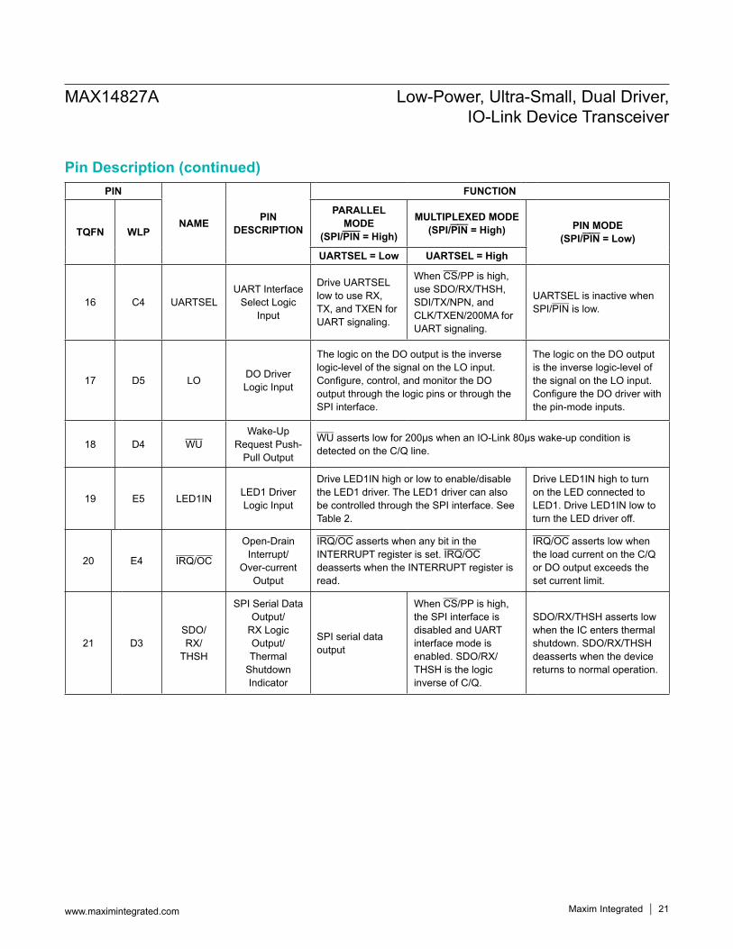
18 D4 WUWake-Up
Request Push-Pull Output
WU asserts low for 200μs when an IO-Link 80μs wake-up condition is detected on the C/Q line.
19 E5 LED1IN LED1 Driver Logic Input
Drive LED1IN high or low to enable/disable the LED1 driver. The LED1 driver can also be controlled through the SPI interface. See Table 2.
Drive LED1IN high to turn on the LED connected to LED1. Drive LED1IN low to turn the LED driver off.
20 E4 IRQ/OC
Open-Drain Interrupt/
Over-current Output
IRQ/OC asserts when any bit in the INTERRUPT register is set. IRQ/OC deasserts when the INTERRUPT register is read.
IRQ/OC asserts low when the load current on the C/Q or DO output exceeds the set current limit.
21 D3SDO/RX/
THSH
SPI Serial Data Output/
RX Logic Output/Thermal
Shutdown Indicator
SPI serial data output
When CS/PP is high, the SPI interface is disabled and UART interface mode is enabled. SDO/RX/THSH is the logic inverse of C/Q.
SDO/RX/THSH asserts low when the IC enters thermal shutdown. SDO/RX/THSH deasserts when the device returns to normal operation.
MAX14827A Low-Power, Ultra-Small, Dual Driver, IO-Link Device Transceiver
www.maximintegrated.com Maxim Integrated 21
Pin Description (continued)

PIN
NAME PIN DESCRIPTION
FUNCTION
TQFN WLP
PARALLEL MODE
(SPI/PIN = High)
MULTIPLEXED MODE(SPI/PIN = High) PIN MODE
(SPI/PIN = Low)UARTSEL = Low UARTSEL = High
22 E3CLK/
TXEN/200MA
SPI Clock Input/
UART TXEN Input/
Current Limit Setting Input
SPI clock input
When CS/PP is high, the SPI interface is disabled and UART interface mode is enabled. Drive CLK/TXEN/200MA high to enable the C/Q driver.
Drive CLK/TXEN/200MA high to enable a 200mA current limit on the C/Q and DO driver outputs. Drive CLK/TXEN/200MA low to set the current limit for the driver outputs to 100mA.
23 D2 SPI/PINSPI or Pin-
Mode Select Input
Drive SPI/PIN high for SPI or UART interface operation. Drive SPI/PIN low for pin-mode operation.
24 E2 SDI/TX/NPN
SPI Serial Data Input/
TX Logic Input/NPN Driver Mode Select
Input
SPI serial data input
When CS/PP is high, the SPI interface is disabled and UART interface mode is enabled. Drive SDI/TX/NPN to switch C/Q. C/Q is the logic inverse of the SDI/TX/NPN input.
Drive SDI/TX/NPN high to set the C/Q and DO driver outputs in NPN mode. Drive SDI/TX/NPN low to set the driver outputs in PNP mode. SDI/TX/NPN is ignored when the CS/PP input is high.
EP - EP Exposed pad. Connect to ground. Not intended as the main ground connection.
MAX14827A Low-Power, Ultra-Small, Dual Driver, IO-Link Device Transceiver
www.maximintegrated.com Maxim Integrated 22
Pin Description (continued)

Table 1. C/Q and DO Control
Table 2: LED1 Configuration Table 3. Driver NPN, PNP, PP Selection in Pin-Mode
X = Don’t care, Z = High impedance
SPI/PIN TXEN TX or LO
CQ_Dis or DO_Dis
CQ_Q or DO_Q
NPN MODE PNP MODE PP MODE
C/Q DO C/Q DO C/Q DO
L
LL - - Z Z Z H Z H
H - - Z L Z Z Z L
HL - - Z Z H H H H
H - - L L Z Z L L
H
L
L 0 0 Z Z Z H Z H
L 0 1 Z Z H H H H
H 0 0 Z L Z Z Z L
H 0 1 Z Z H H H H
H
L 0 0 Z Z H H H H
L 0 1 Z Z H H H H
H 0 0 L L Z Z L L
H 0 1 Z Z H H H H
X X 1 X Z Z Z Z Z Z
LED1IN LED1b BIT LED1 DRIVER STATUS
L0 OFF
1 ON
H0 ON
1 ON
SPI/PIN CS/PP SDI/TX/NPN C/Q AND DO DRIVER MODE
L L L PNP
L L H NPN
L H L PUSH-PULL
L H H PUSH-PULL
H X XC/Q and DO Modes are set with the SPI
interface
MAX14827A Low-Power, Ultra-Small, Dual Driver, IO-Link Device Transceiver
www.maximintegrated.com Maxim Integrated 23
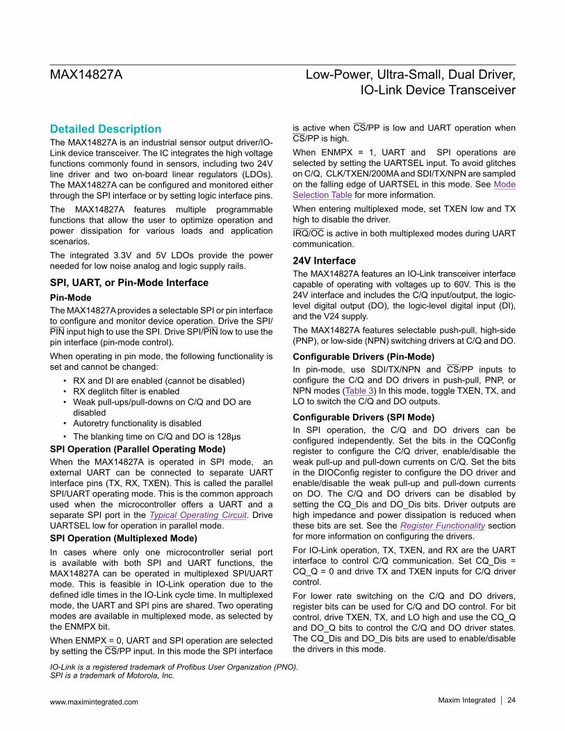
Detailed DescriptionThe MAX14827A is an industrial sensor output driver/IO-Link device transceiver. The IC integrates the high voltage functions commonly found in sensors, including two 24V line driver and two on-board linear regulators (LDOs). The MAX14827A can be configured and monitored either through the SPI interface or by setting logic interface pins. The MAX14827A features multiple programmable functions that allow the user to optimize operation and power dissipation for various loads and application scenarios.The integrated 3.3V and 5V LDOs provide the power needed for low noise analog and logic supply rails.
SPI, UART, or Pin-Mode InterfacePin-ModeThe MAX14827A provides a selectable SPI or pin interface to configure and monitor device operation. Drive the SPI/PIN input high to use the SPI. Drive SPI/PIN low to use the pin interface (pin-mode control).When operating in pin mode, the following functionality is set and cannot be changed:
• RX and DI are enabled (cannot be disabled)• RX deglitch filter is enabled• Weak pull-ups/pull-downs on C/Q and DO are
disabled• Autoretry functionality is disabled• The blanking time on C/Q and DO is 128μs
SPI Operation (Parallel Operating Mode)When the MAX14827A is operated in SPI mode, an external UART can be connected to separate UART interface pins (TX, RX, TXEN). This is called the parallel SPI/UART operating mode. This is the common approach used when the microcontroller offers a UART and a separate SPI port in the Typical Operating Circuit. Drive UARTSEL low for operation in parallel mode.SPI Operation (Multiplexed Mode) In cases where only one microcontroller serial port is available with both SPI and UART functions, the MAX14827A can be operated in multiplexed SPI/UART mode. This is feasible in IO-Link operation due to the defined idle times in the IO-Link cycle time. In multiplexed mode, the UART and SPI pins are shared. Two operating modes are available in multiplexed mode, as selected by the ENMPX bit. When ENMPX = 0, UART and SPI operation are selected by setting the CS/PP input. In this mode the SPI interface
is active when CS/PP is low and UART operation when CS/PP is high. When ENMPX = 1, UART and SPI operations are selected by setting the UARTSEL input. To avoid glitches on C/Q, CLK/TXEN/200MA and SDI/TX/NPN are sampled on the falling edge of UARTSEL in this mode. See Mode Selection Table for more information. When entering multiplexed mode, set TXEN low and TX high to disable the driver.IRQ/OC is active in both multiplexed modes during UART communication.
24V InterfaceThe MAX14827A features an IO-Link transceiver interface capable of operating with voltages up to 60V. This is the 24V interface and includes the C/Q input/output, the logic-level digital output (DO), the logic-level digital input (DI), and the V24 supply.The MAX14827A features selectable push-pull, high-side (PNP), or low-side (NPN) switching drivers at C/Q and DO.
Configurable Drivers (Pin-Mode)In pin-mode, use SDI/TX/NPN and CS/PP inputs to configure the C/Q and DO drivers in push-pull, PNP, or NPN modes (Table 3) In this mode, toggle TXEN, TX, and LO to switch the C/Q and DO outputs.
Configurable Drivers (SPI Mode)In SPI operation, the C/Q and DO drivers can be configured independently. Set the bits in the CQConfig register to configure the C/Q driver, enable/disable the weak pull-up and pull-down currents on C/Q. Set the bits in the DIOConfig register to configure the DO driver and enable/disable the weak pull-up and pull-down currents on DO. The C/Q and DO drivers can be disabled by setting the CQ_Dis and DO_Dis bits. Driver outputs are high impedance and power dissipation is reduced when these bits are set. See the Register Functionality section for more information on configuring the drivers.For IO-Link operation, TX, TXEN, and RX are the UART interface to control C/Q communication. Set CQ_Dis = CQ_Q = 0 and drive TX and TXEN inputs for C/Q driver control. For lower rate switching on the C/Q and DO drivers, register bits can be used for C/Q and DO control. For bit control, drive TXEN, TX, and LO high and use the CQ_Q and DO_Q bits to control the C/Q and DO driver states. The CQ_Dis and DO_Dis bits are used to enable/disable the drivers in this mode.
IO-Link is a registered trademark of Profibus User Organization (PNO).SPI is a trademark of Motorola, Inc.
MAX14827A Low-Power, Ultra-Small, Dual Driver, IO-Link Device Transceiver
www.maximintegrated.com Maxim Integrated 24

C/Q Driver Enable/DisableIn pin-mode, the C/Q driver is enabled/disabled with the TXEN input. Drive TXEN high to enable the C/Q driver. C/Q is the logic inverse of the TX input. In SPI mode, the C/Q driver can also be enabled/disabled, configured, and controlled in the CQConfig register.
C/Q Current LimitThe C/Q driver is optimized for driving large capacitive loads and dynamic impedances like incandescent lamps. In pin-mode, the driver current limit is selectable by setting the CLK/TXEN/200MA input high or low. Set CLK/TXEN/200MA low for 100mA maximum load current. Set CLK/TXEN/200MA high for a 200mA maximum load current. In SPI operation, the maximum driver current limit is selectable as 50mA, 100mA, 200mA, or 250mA by setting the CL1 and CL0 bits in the CURRLIM register.
C/Q Driver Fault DetectionThe MAX14827A senses a fault condition on the C/Q driver when it detects a short circuit for longer than the blanking time. A short condition exists when the C/Q driver’s load current exceeds the current limit. In SPI mode, both the current limit and blanking time may be configured.In pin-mode, the IRQ/OC output asserts low when a short circuit fault occurs on C/Q or DO. In SPI mode, the C/QFault and C/QFaultInt bits are set and IRQ/OC asserts.When a short-circuit event occurs on C/Q, the driver can either be set to continue supplying the selected current until the device enters thermal shutdown or to enter autoretry mode when an overcurrent event occurs. In autoretry mode the driver is automattically disabled after the current blanking time and is then re-enabled.
C/Q Receiver Output (RX)RX is the output of the C/Q receiver. RX is the inverse logic of the C/Q input. In pin-control mode, the C/Q receiver is always on. In SPI mode, the receiver can be disabled by setting the Rx_Dis bit in the CQConfig register. RX is high impedance when Rx_Dis is set. Note that the CQLvl bit in the Status register is invalid when the Rx_Dis bit is set. When operating in multiplexed mode, SDO/RX/THSH is the output of the C/Q receiver. In this mode, SDO/RX/THSH is high impedance when CS/PP is high and Rx_Dis bit is set.
C/Q Receiver ThresholdThe IO-Link standard defines device operation with a sensor supply between 18V and 30V. Industrial sensors, however, commonly operate with supply voltages as low as 9V. The MAX14827A C/Q receiver supports operation with lower supply voltages by scaling the receiver thresholds when V24 is less than 18V (V24 < 18V).
DO DriverIn pin-mode, the DO driver is always enabled. DO is the logic inverse of the LO input. In SPI mode, the DO driver can be enabled/disabled, configured, and controlled in the DIOConfig register.
DO Current LimitThe DO driver is optimized for driving large capacitive loads and dynamic impedances like incandescent lamps. In pin-control mode, the driver current limit is selectable by setting the CLK/TXEN/200MA input high or low. Set CLK/TXEN/200MA low for 100mA maximum load current. Set CLK/TXEN/200MA high for a 200mA maximum load current.In SPI operation, the maximum driver current limit is selectable as 50mA, 100mA, 200mA, or 250mA by setting the CL1 and CL0 bits in the CURRLIM register.
DO Fault DetectionThe MAX14827A senses a fault condition on the DO output when it detects a short circuit for longer than the blanking time. A short condition exists when the DO driver’s load current exceeds the current limit. In SPI mode, both the current limit and blanking time may be configured.In pin-mode, the IRQ/OC output asserts low when a short circuit fault occurs on C/Q or DO. In SPI mode, the DoFault and DoFaultInt bits are set and IRQ/OC asserts.When a short-circuit event occurs on DO, the driver can either be set to continue supplying the selected current until the device enters thermal shutdown or to enter autoretry mode when an overcurrent event occurs. In autoretry mode the driver is automattically disabled after the current blanking time and is then re-enabled.DO and C/Q TrackingIn SPI mode, the DO driver can be configured to track the C/Q driver. Set the CQDOPar bit in the CQConfig register to enable this functionality. When the DO driver is set to track C/Q, both C/Q and DO switch as a function of the TX and TXEN inputs or CQ_Q bit.In pin-mode, or when CQDOPar is 0, C/Q and DO operate independently.
MAX14827A Low-Power, Ultra-Small, Dual Driver, IO-Link Device Transceiver
www.maximintegrated.com Maxim Integrated 25

Reverse-Polarity ProtectionThe MAX14827A is protected against reverse-polarity connections on V24, C/Q, DO, DI, and GND. Any combination of these pins can be connected to DC voltages up to 65V (max), resulting in a current flow of less than 1mA.Ensure that the maximum voltage between any of these pins does not exceed 65V.
Driver Short-Circuit DetectionThe MAX14827A monitors the DO and C/Q driver outputs for overcurrent and driver overheating conditions. In pin-mode, the driver short-circuit current limit is set with the CLK/TXEN/200mA input. IRQ/OC asserts when an overcurrent or overheating condition occurs on either the C/Q or DO driver. IRQ/OC deasserts when the overcurrent or overheating condition is removed. In SPI mode, the DO and C/Q are independently monitored. Driver current limits for both drivers are set using the CL1 and CL0 bits in the CURRLIM register. When an overcurrent or overheating condition occurs on C/Q, the CQFault and CQFaultInt bits are set and IRQ/OC asserts. When an overcurrent or overheating condition occurs on DO, the DOFault and DOFaultInt bits are set. The CQFault and DOFault bits are cleared as soon as the overcurrent or overheating conditions on the C/Q and DO drivers are removed. IRQ/OC deasserts and the CQFaultInt and DOFaultInt bits are cleared only when the INTERRUPT register is read.
5V and 3.3V Linear RegulatorsThe MAX14827A includes two internal regulators to generate 5V (V5) and 3.3V (V33). The V5 regulator is capable of driving external loads up to 30mA, including device and 3.3V LDO current consumption. To drive larger loads, use an external pass transistor to generate the required 5V. When using an external transistor, connect REG to the base of the transistor to regulate the voltage and connect V5 to the emitter (Figure 10 ).When the internal 5V linear regulator is not used, V5 is the supply input for the internal analog and digital functions and must be supplied externally. Ensure that V5 is present for normal operation.The 3.3V regulator is capable of driving external loads up to 30mA. In SPI mode, the 3.3V LDO can be enabled/disabled by setting the V33Dis bit in the Mode register. V5 and V33 are not protected against short circuits.
Power-UpThe C/Q and DO driver outputs are high impedance when V24, V5, VL, and/or V33 voltages are below their respective undervoltage thresholds during power-up.The drivers are automatically disabled if V24, V5, or VL falls below its threshold.
Low Voltage and Undervoltage DetectionIn SPI mode, the device monitors the V24 supply for low voltage and undervoltage conditions. Low-voltage warnings must be enabled in the MODE register.When V24 falls below the 16V (typ) low-voltage warning threshold, the V24W bit in the STATUS register is set. If V24WEn is set to 1, the V24WInt interrupt bit is also set and IRQ/OC asserts.When V24 falls below the 7.4V (typ) undervotlage lockout (UVLO) threshold, the UV24 bit in the STATUS register is set. Similarly, the UV24Int bit in the INTERRUPT register is set and IRQ/OC asserts. UVLO monitoring and interrupts cannot be disabled.
Wake-Up DetectionThe MAX14827A detects an IO-Link wake-up condition on the C/Q line in push-pull, high-side (PNP), or low-side (NPN) operation modes. A wake-up condition is detected when the C/Q output is shorted for 80µs (typ). WU pulses low for 200µs (typ) when the device detects a wake-up pulse on C/Q (Figure 5).In SPI mode, the WuInt bit in the INTERRUPT registeris set and IRQ/OC asserts when an IO-Link wake-up event is detected. Wake-up detection can be disabled in SPI mode by setting the WU_Dis bit in the MODE register to 0. Wake-up detection cannot be disabled in pin-mode.The device includes a wake-up detection algorithm to avoid false wake-up detection on C/Q. The false wake-up blanking time is defined by the current limit blanking time. In pin-mode, this is 128μs. In SPI-mode, this is set by the CL_BL0 and CL_BL1 bits in the CURRLIM reigster.
Thermal Protection and ConsiderationsThe internal LDOs and drivers can generate more power than the package for the devices can safely dissipate. Ensure that the driver and LDO loading is less than the package can dissipate. Total power dissipation for the device is calculated using the following equation:
PTOTAL = PC/Q + PDO + PV5 + P33 + P24 + (2 x PPU) + (2 x PPD)
MAX14827A Low-Power, Ultra-Small, Dual Driver, IO-Link Device Transceiver
www.maximintegrated.com Maxim Integrated 26

where PC/Q is the power generated in the C/Q driver, PDO is the power dissipated by the DO driver, PV5 and PV33 are the power generated by the LDOs, P24 is the quiescent power generated by the device, and PPU and PPD are the power generated in the C/Q and DO weak pullup/pulldown current sources/sinks, respectively.Ensure that the total power dissipation is less than the limits listed in the Absolute Maximum Ratings section.Use the following to calculate the power dissipation (in mW) due to the C/Q driver:
PC/Q = [IC/Q(max)]2 × ROwhere RO driver on-resistance.Calculate the internal power dissipation of the DO driver using the following equation:
PDO = [IDO(max)]2 x ROwhere RO driver on-resistance.Calculate the power dissipation in the 5V LDO, V5, using the following equation:
P5 = (V24 - V5) × I5where I5 includes the I33 current sourced from V33.Calculate the power dissipated in the 3.3V LDO, V33, using the following equation:
P33 = 1.7V × ILOAD33Calculate the quiescent power dissipation in the device using the following equation:
P24 = I24(max) × V24(max)If the weak current sinks/sources are enabled, calculate their associated power dissipation as:
PPD = IPD(max) × VC/Q (max) PPU = IPU(max) × [V24 - VC/Q](max)
Overtemperature WarningIn SPI mode, the device generates interrupts when the junction temperature of any of the drivers (C/Q or DO) exceeds +140°C (typ) warning threshold. The TempW bit in the STATUS register is set and the TempWInt in the INTERRUPT register is set and IRQ/OC asserts under these conditions.The TempW bit is cleared when the die temperature falls to +125°C. The INTERRUPT register must be read to clear the TempWInt bit and deassert IRQ/OC.The device continues to operate normally unless the die temperature reaches the +165°C thermal shutdown threshold, when the device enters thermal shutdown.The device does not generate overtemperature warnings when operating in pin-mode.
Thermal ShutdownThe C/Q and DO drivers, and the V5 and V33 regulators are automatically switched off when the junction temperature exceeds the +165°C (typ) thermal shutdown threshold. SPI communication and and the internal regulators are not disabled during thermal shutdown. In SPI mode, the ThShut bit in the STATUS register and the ThShutInt in the INTERRUPT register are set.Regulators are automatically switched on when the internal die temperature falls below the thermal shutdown threshold plus hysteresis. If the internal V5 regulator is used, the internal registers return to their default state when the V5 regulator is switched back on.
MAX14827A Low-Power, Ultra-Small, Dual Driver, IO-Link Device Transceiver
www.maximintegrated.com Maxim Integrated 27

Mode Selection TableOPERATING
MODESPI/ PIN UARTSEL ENMPX
Bit CS/PP PIN NAME PIN FUNCTION FUNCTION
PIN L X XLOW OR
HIGH
SDI/TX/NPN NPN Parallel configuration/monitoring
SDO/RX/THSH THSH Parallel configuration/monitoring
CLK/TXEN/200MA 200MA Parallel configuration/monitoring
CS/PP PP Parallel configuration/monitoring
IRQ/OC OC Parallel configuration/monitoring
RX C/Q RXParallel configuration/monitoring/UART communication
TX C/Q TXParallel configuration/monitoring/UART communication
TXEN C/Q TXENParallel configuration/monitoring/UART communication
PARALLEL UART + SPI
H L 0LOW OR
HIGH
SDI/TX/NPN SDI SPI configuration/monitoring
SDO/RX/THSH SDO SPI configuration/monitoring
CLK/TXEN/200MA CLK SPI configuration/monitoring
CS/PP CS SPI configuration/monitoring
IRQ/OC IRQ SPI configuration/monitoring
RX C/Q RX UART communication
TX C/Q TX UART communication
TXEN C/Q TXEN UART communication
MULTIPLEXED UART/SPI
H H 0
L
SDI/TX/NPN SDI SPI configuration/monitoring
SDO/RX/THSH SDO SPI configuration/monitoring
CLK/TXEN/200MA CLK SPI configuration/monitoring
CS/PP LOW SPI configuration/monitoring
IRQ/OC IRQ SPI configuration/monitoring
RX C/Q RX UART communication
TX C/Q TX UART communication
TXEN C/Q TXEN UART communication
H
SDI/TX/NPN C/Q TX UART communication
SDO/RX/THSH C/Q RX UART communication
CLK/TXEN/200MA C/Q TXEN UART communication
CS/PP HIGH
IRQ/OC IRQ SPI configuration/monitoring
RX C/Q RX Active
TX C/Q TX Ignored
TXEN C/Q TXEN Ignored
MAX14827A Low-Power, Ultra-Small, Dual Driver, IO-Link Device Transceiver
www.maximintegrated.com Maxim Integrated 28
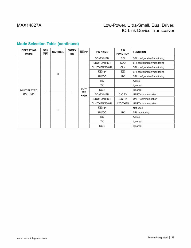
Mode Selection Table (continued)OPERATING
MODESPI/ PIN UARTSEL ENMPX
Bit CS/PP PIN NAME PIN FUNCTION FUNCTION
MULTIPLEXED UART/SPI
H
0
1LOW OR
HIGH
SDI/TX/NPN SDI SPI configuration/monitoring
SDO/RX/THSH SDO SPI configuration/monitoring
CLK/TXEN/200MA CLK SPI configuration/monitoring
CS/PP CS SPI configuration/monitoring
IRQ/OC IRQ SPI configuration/monitoring
RX Active
TX Ignored
TXEN Ignored
1
SDI/TX/NPN C/Q TX UART communication
SDO/RX/THSH C/Q RX UART communication
CLK/TXEN/200MA C/Q TXEN UART communication
CS/PP Not used
IRQ/OC IRQ SPI monitoring
RX Active
TX Ignored
TXEN Ignored
MAX14827A Low-Power, Ultra-Small, Dual Driver, IO-Link Device Transceiver
www.maximintegrated.com Maxim Integrated 29

Table 4. Register Summary
INTERRUPT Register [A2, A1, A0] = [000]
Register FunctionalityThe devices have four 8-bit-wide registers for configuration and monitoring (Table 1).
Bit Bit 7 Bit 6 Bit 5 Bit 4 Bit 3 Bit 2 Bit 1 Bit 0Bit Name ThShutInt WuInt DoFaultInt CQFaultInt V24WInt UV24Int - TempWIntRead/Write R R R R R R R RPOR State 0 0 0 0 0 0 0 0Reset Upon Read N N N N N N N N
The INTERRUPT register reflects current state of various fault conditions. The IRQ/OC output asserts when any of the bits in the INTERRUPT register is set. INTERRUPT register bits are latched and are not cleared when the initiating condition is removed. Reading the INTERRUPT register clears all the bits and deasserts IRQ/OC. IRQ/OC reasserts only when another fault condition occurs.
BIT NAME DESCRIPTION
7 ThShutInt
Thermal Shutdown Interrupt 1: This bit is set when the MAX14827A has entered thermal shutdown mode. Once set,
this bit is not cleared until the register is read. The current status of the thermal shutdown condition can be read in the Status register.
0: The MAX14827A is not in thermal shutdown.
6 WuInt
Wake-Up Event Interrupt1: This bit is set when an IO-Link wake-up condition is detected on the C/Q line. 0: No wake-up condition is detected.The wake-up interrupt can be disabled by setting the WuDis bit to 1.
REGISTER ADD R/W BIT 7 BIT 6 BIT 5 BIT 4 BIT 3 BIT 2 BIT 1 BIT 0INTERRUPT 00h R ThShutInt WuInt DoFaultInt CQFaultInt V24WInt UV24Int - TempWInt
STATUS 01h R ThShut DiLvl DoFault CQFault V24W UV24 CQLvl TempW
MODE 02h R/W RST WU_Dis V33_Dis ENMPX V24WEn CQFil LED2b LED1b
CURRLIM 03h R/W CL1 CL0 CLDis CL_BL1 CL_BL0 TAr1 TAr0 ArEn
CQConfig 04h R/W Rx_Dis CQ_WPD CQ_WPU CQDOPar CQ_NPN CQ_PP CQ_Q CQ_Dis
DIOConfig 05h R/W DI_Dis DO_WPD DO_WPU DO_AV DO_NPN DO_PP DO_Q DO_Dis
MAX14827A Low-Power, Ultra-Small, Dual Driver, IO-Link Device Transceiver
www.maximintegrated.com Maxim Integrated 30

INTERRUPT Register [A2, A1, A0] = [000] (continued)
BIT NAME DESCRIPTION
5 DoFaultInt
DO Driver Fault Interrupt 1: This bit is set when a fault occurs on the DO driver (over current or over heating).
Once set, this bit is not cleared until the register is read. The current status of the thermal shutdown condition can be read in the Status register.
0: No fault on the DO driver.
4 CQ_FaultInt
C/Q Driver Fault Interrupt 1: This bit is set when a fault occurs on the C/Q driver (over current or over heating).
Once set, this bit is not cleared until the register is read. The current status of the thermal shutdown condition can be read in the Status register.
0: No fault on the C/Q driver.
3 V24WInt
V24 Low Voltage Warning Interrupt 1: This bit is set when V24 falls below the IO-Link low-voltage warning threshold fault
(V24 < V24W). Once set, this bit is not cleared until the register is read. The current status of the thermal shutdown condition can be read in the Status register.
0: V24 is greater than the low-voltage warning threshold.
2 UV24Int
V24 Supply Undervoltage Interrupt 1: This bit is set when V24 falls below the UVLO threshold (V24 < V24UVLO). Once
set, this bit is not cleared until the register is read. The current status of the thermal shutdown condition can be read in the Status register.
0: V24 is greater than the UVLO threshold.
1 This bit is not used.
0 TempWInt
Overtemperature Warning Interrupt1: This bit is set when the die temperature exceeds the warning threshold (TJ > TWRN).
Once set, this bit is not cleared until the register is read. The current status of the thermal shutdown condition can be read in the Status register.
0: The die temperature has not exceeded the overtemperature warning threshold.
MAX14827A Low-Power, Ultra-Small, Dual Driver, IO-Link Device Transceiver
www.maximintegrated.com Maxim Integrated 31

STATUS Register [A2, A1, A0] = [001]Bit Bit 7 Bit 6 Bit 5 Bit 4 Bit 3 Bit 2 Bit 1 Bit 0Bit Name ThShut DiLvl DoFault CQFault V24W UV24 CQLvl TempWRead/Write R R R R R R R RPOR State 0 0 0 0 0 0 0 0Reset Upon Read N N N N N N N N
The Status register reflects current state of various IC functions.
BIT NAME DESCRIPTION
7 ThShutThermal Shutdown Status 1: This bit is set when the MAX14827A has entered thermal shutdown mode. 0: This bit is cleared automatically when the device exits thermal shutdown.
6 DiLvlDI Logic Level 1: This bit is set when the DI voltage is a logic high (VDI < VTL). 0: This bit is clear when the DI voltage is a logic low (VDI > VTH).
5 DoFaultDO Driver Fault Status 1: This bit is set when a fault occurs on the DO driver (over current or over heating). 0: This bit is cleared automatically when the fault on DO is removed.
4 CQ_FaultC/Q Driver Fault Status 1: This bit is set when a fault occurs on the C/Q driver (over current or over heating). 0: This bit is cleared automatically when the fault on C/Q is removed.
3 V24W
V24 Low Voltage Warning Status 1: This bit is set when V24 falls below the IO-Link low-voltage warning threshold (V24 <
V24W). 0: This bit is cleared automatically when V24 rises above the low-voltage warning
threshold.
2 UV24V24 Supply Status 1: This bit is set when V24 falls below the UVLO threshold (V24 < V24UVLO). 0: This bit is cleared automatically when V24 rises above the UVLO threshold.
1 CQLvlC/Q Logic Level 1: This bit is set when the C/Q voltage is a logic high (VC/Q < VTL). 0: This bit is clear when the C/Q voltage is a logic low (VC/Q > VTH).
0 TempW
Overtemperature Warning1: This bit is set when the die temperature exceeds the warning threshold (TJ > TWRN). 0: This bit is cleared automatically when the when the die temperature falls below the warning threshold and hysteresis (TJ < TWRN - TWRN_HYST).
MAX14827A Low-Power, Ultra-Small, Dual Driver, IO-Link Device Transceiver
www.maximintegrated.com Maxim Integrated 32

MODE Register [A2, A1, A0] = [010]Bit Bit 7 Bit 6 Bit 5 Bit 4 Bit 3 Bit 2 Bit 1 Bit 0Bit Name RST WU_Dis V33_Dis ENMPX V24WEn CQFil LED2b LED1bRead/Write R/W R/W R/W R/W R/W R/W R/W R/WPOR State 0 0 0 0 0 0 0 0Reset upon Read N N N N N N N N
Use the Mode register to configure the MAX14827A and manage the 3.3V LDO.
BIT NAME DESCRIPTION
7 RST
Register Reset 1: Reset all registers to their default power-up state. The Status register is
cleared and IRQ deasserts (if asserted) when RST = 1. Interrupts are not generated while RST = 1.
0: Normal operation.
6 WU_DisWake-Up Interrupt Disable/Enable 1: Wake-up detection is disabled. 0: Enable IO-Link wake-up detection.
5 V33_DisV33 Enable/Disable 1: Disable the V33 linear regulator. 0: Enable the V33 linear regulator.
4 ENMPX
Enable/Disable SPI/UART Multiplexing1: Enable UART multiplexing on SPI interface pins. See the Mode Selection
Table for more information.0: Disable UART multiplexing on SPI interface pins.
3 V24WEn
V24 Undervoltage Warning Enable 1: Enable the V24 undervoltage warning interrupt. V24WInt is set when V24 falls
below the UVLO threshold.0: Disable the V24 undervoltage warning interrupt.
2 CQFilC/Q Deglitch Filter Enable/Disable1: Deglitch filter is disabled on RX. 0: Deglitch filter is enabled on RX.
1 LED2bLED2 Driver Logic1: Set the LED2 output high.0: Set the LED2 output low.
0 LED1bLED1 Driver Logic. 1: Set the LED1 output high.0: LED1 output is driven by the LED1IN logic input.
MAX14827A Low-Power, Ultra-Small, Dual Driver, IO-Link Device Transceiver
www.maximintegrated.com Maxim Integrated 33

CURRLIM Register [A2, A1, A0] = [011]Bit Bit 7 Bit 6 Bit 5 Bit 4 Bit 3 Bit 2 Bit 1 Bit 0Bit Name CL1 CL0 CL_Dis CL_BL1 CL_BL0 TAr1 TAr0 ArENRead/Write R/W R/W R/W R/W R/W R/W R/W R/WPOR State 0 0 0 0 0 0 0 0Reset Upon Read N N N N N N N N
The CURRLIM register sets the C/Q and DO driver current limits and the fixed off-time once the drivers have exceeded their individual thermal shutdown thresholds.
BIT NAME DESCRIPTION
7 CL1Driver Current Limit Set the CL1 and CL0 bits to select the active current limit for the C/Q and DO drivers when CL_Dis = 0.
00: Driver current limit is set to 50mA01: Driver current limit is set to 100mA10: Driver current limit is set to 200mA11: Driver current limit is set to 250mA
6 CL0
5 CL_DisDriver Current Limit Disable/Enable1: Disable the driver current limit for the C/Q and DO drivers.0: Enable the driver current limit (as set by the CL1 and CL0 bits).
4 CL_BL1Current Limit Blanking Time Set the CL_BL1 and CL_BL0 bits to select the minimum blanking time to signal a current limit or thermal fault.
00: Blanking time is 128μs01: Blanking time is 500μs10: Blanking time is 1ms11: Blanking time is 5ms
3 CL_BL0
2 TAr1
Auto-Retry Fixed Off-Time Set the TAr1 and TAr0 bits to select the fixed driver off-time after a fault has been generated when auto-retry functionality is enabled (ArEn = 1). The driver is re-enabled automatically after the fixed off-delay.
00: Fixed off-time is 50ms01: Fixed off-time is 100ms10: Fixed off-time is 200ms11: Fixed off-time is 500ms
1 TAr0
0 ArEN
Auto-Retry Fixed Off-Time Enable/Disable1: Fixed off-time functionality is enabled. C/Q and DO drivers are disabled for a
fixed time after an overcurrent or thermal fault occurs. The driver is re-enabled automatically after the fixed off-delay.
0: Fixed off-time functionality is disabled. The driver is re-enabled after temperature falls below the thermal hysteresis.
MAX14827A Low-Power, Ultra-Small, Dual Driver, IO-Link Device Transceiver
www.maximintegrated.com Maxim Integrated 34
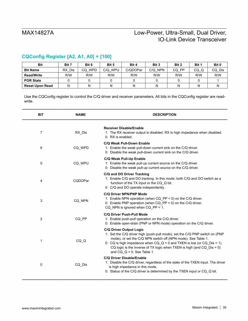
CQConfig Register [A2, A1, A0] = [100]Bit Bit 7 Bit 6 Bit 5 Bit 4 Bit 3 Bit 2 Bit 1 Bit 0
Bit Name RX_Dis CQ_WPD C/Q_WPU C/QDOPar C/Q_NPN CQ_PP CQ_Q CQ_DisRead/Write R/W R/W R/W R/W R/W R/W R/W R/WPOR State 0 0 0 0 0 0 0 1Reset Upon Read N N N N N N N N
Use the CQConfig register to control the C/Q driver and receiver parameters. All bits in the CQConfig register are read-write.
BIT NAME DESCRIPTION
7 RX_DisReceiver Disable/Enable1: The RX receiver output is disabled. RX is high impedance when disabled. 0: RX is enabled.
6 CQ_WPDC/Q Weak Pull-Down Enable 1: Enable the weak pull-down current sink on the C/Q driver.0: Disable the weak pull-down current sink on the C/Q driver.
5 CQ_WPUC/Q Weak Pull-Up Enable1: Enable the weak pull-up current source on the C/Q driver.0: Disable the weak pull-up current source on the C/Q driver.
4 CQDOPar
C/Q and DO Driver Tracking1: Enable C/Q and DO tracking. In this mode, both C/Q and DO switch as a
function of the TX input or the CQ_Q bit.0: C/Q and DO operate independently.
3 CQ_NPN
C/Q Driver NPN/PNP Mode 1: Enable NPN operation (when CQ_PP = 0) on the C/Q driver. 0: Enable PNP operation (when CQ_PP = 0) on the C/Q driver. CQ_NPN is ignored when CQ_PP = 1.
2 CQ_PPC/Q Driver Push-Pull Mode1: Enable push-pull operation on the C/Q driver. 0: Enable open-drain (PNP or NPN mode) operation on the C/Q driver.
1 CQ_Q
C/Q Driver Output Logic 1: Set the C/Q driver high (push-pull mode), set the C/Q PNP switch on (PNP
mode), or set the C/Q NPN switch off (NPN mode). See Table 1.0: CQ is high impedance when CQ_Q = 0 and TXEN is low (or CQ_Dis = 1).
CQ logic is the inverse of TX logic when TXEN is high (and CQ_Dis = 0) and CQ_Q = 0. See Table 1.
0 CQ_Dis
C/Q Driver Disable/Enable1: Disable the C/Q driver, regardless of the state of the TXEN input. The driver
is high impedance in this mode.0: Status of the C/Q driver is determined by the TXEN input or CQ_Q bit.
MAX14827A Low-Power, Ultra-Small, Dual Driver, IO-Link Device Transceiver
www.maximintegrated.com Maxim Integrated 35

DIOConfig Register [A2, A1, A0] = [101]Bit Bit 7 Bit 6 Bit 5 Bit 4 Bit 3 Bit 2 Bit 1 Bit 0Bit Name DI_Dis DO_WPD DO_WPU DO_AV DO_NPN DO_PP DO_Q DO_DisRead/Write R/W R/W R/W R/W R/W R/W R/W R/WPOR State 0 0 0 0 0 0 0 1Reset Upon Read N N N N N N N N
Use the DIOConfig register to control the DI and DO interfaces. All bits in the DIOConfig register are read-write.
BIT NAME DESCRIPTION
7 DI_Dis
DI Receiver Enable/Disable 1: The DI receiver is disabled. LI is high impedance when the DI receiver is disabled.0: DI receiver is enabled.
6 DO_WPDDO Weak Pulldown Enable
1: Enable the weak pull-down current sink on the DO driver.0: Disable the weak pull-down current sink on the DO driver.
5 DO_WPUDO Weak Pullup Enable
1: Enable the weak pull-up current source on the DO driver.0: Disable the weak pull-up current source on the DO driver.
4 DO_AV
DO Antivalent Operation 1: Enable antivalent operation on the C/Q and DO outputs. In this
mode, DO switches as a function of the LO input or the DO_Q bit, but with opposite logic. If CQDOPar = 1, both C/Q and DO switch as a function of TX and/or CQ_Q, but with opposite logic.
0: C/Q and DO switch with normal polarity.
3 DO_NPN
DO Driver NPN/PNP Mode 1: Enable NPN operation (when DO_PP = 0) on the DO driver. 0: Enable PNP operation (when DO_PP = 0) on the DO driver.
DO_NPN is ignored when DO_PP = 1.
2 DO_PPDO Driver Push-Pull Mode
1: Enable push-pull operation on the DO driver. 0: Enable open-drain (PNP or NPN mode) operation on the DO driver.
1 DO_Q
DO Driver Output Logic1: Set the DO driver high (push-pull mode), set the DO PNP switch on
(PNP mode), or set the DO NPN switch off (NPN mode). See Table 1.0: DO logic is the inverse of LO logic when DO_Dis = 0 and DO_Q = 0.
See Table 1.
0 DO_DisDO Driver Disable/Enable
1: Disable the DO driver. DO is high impedance when disabled. 0: State of the DO driver is determined by the LO input or the DO_Q bit.
MAX14827A Low-Power, Ultra-Small, Dual Driver, IO-Link Device Transceiver
www.maximintegrated.com Maxim Integrated 36

SPI InterfaceThe device communicates through an SPI-compatible 4-wire serial interface. The MAX14827A supports burst read/write access. The maximum SPI clock rate for the device is 12MHz. The SPI interface complies with clock
polarity CPOL = 0 and clock phase CPHA = 0 (see Figure 7 and Figure 8).The SPI interface is not available when V5 or VL are not present.
Figure 7. SPI Write Cycle
Figure 8. SPI Read Cycle
CS/PP
CLK/TXEN/200MA
SDI/TX/NPN W 0 0 0 0 A2 A1 A0 BIT 7 BIT 6 BIT 5 BIT 4 BIT 3 BIT 2 BIT 1 BIT 0
A_ = REGISTER ADDRESS
BIT_ = DATA BIT
= CLOCK EDGE THAT INTIATES LATCHING OF SDI DATA
CS/PP
CLK/TXEN/200MA
SDI/TX/NPN R 0 0 0 0 A2 A1 A0
BIT 7
X
BIT 6 BIT 5 BIT 4 BIT 3 BIT 2 BIT 1 BIT 0
X
SDO/RX/THSH
A_ = REGISTER ADDRESS
BIT_ = DATA BIT
= CLOCK EDGE THAT INTIATES LATCHING OF SDI DATA
= CLOCK EDGE THAT INTIATES WRITING OF SDO DATA
MAX14827A Low-Power, Ultra-Small, Dual Driver, IO-Link Device Transceiver
www.maximintegrated.com Maxim Integrated 37

SPI Burst AccessBurst access allows writing or reading in one block, by only defining the initial register address in the SPI command byte. Once the initial SPI address is received, the MAX14827A automatically increments the register after each SPI data byte. Efficient programming of multiple consecutive registers is thus possible. Chip select, CS/PP, must be kept low during the whole write/read cycle.The SPI clock continues clocking throughout the burst access cycle. The burst cycle ends when the SPI master pulls CS/PP high.
Applications InformationMicrocontroller InterfacingThe logic levels of the microcontroller interface I/Os are defined by VL. Apply a voltage from 2.5V to 5.5V to VL for normal operation. Logic outputs are supplied by VL.The device can be configured for simultaneous or multiplexed UART communication. When configured for a multipexed UART interface, the SPI interface and UART interface pins are shared. See the Mode Selection Table for more information.
Transient ProtectionInductive load switching, ESD, bursts, and surges create high transient voltages. V24, C/Q, DI, and DO should be protected against high overvoltage and undervoltage transients. Positive voltage transients on V24, C/Q, DO, and DI must be limited to +70V relative to GND. Negative voltage transients must be limited to -70V relative to V24. Use protection diodes on C/Q, DO, and DI as shown in Figure 9.For standard ESD and burst protection demanded by the IO-Link specification, small package TVS can be used (like the uClamp3603T or the SPT01-335). If higher level surge ratings need to be achieved (IEC 61000-4-5 ±1kV/ 42Ω), SMAJ33A or SMBJ36A TVS protectors can also be used.
Using an External Transistor with the 5V Regulator The internal 5V regulator (V5) can provide up to 30mA of total load current (including the current on to the V33 LDO) when V5 is connected to REG. To achieve larger
load currents or to shunt the power dissipation away from the MAX14827A, an external NPN transistor can be connected as shown in Figure 10.Select an NPN transistor with high VCE voltage to support the max L+ supply voltage. In order to protect the NPN transistor against reverse polarity of the L+/L- supply terminals, connect a silicon or a Schottky diode in series with the NPN transistor’s collector that has a reverse voltage capability large enough for reverse connected L+/L-. A 1µF capacitor on the V5 is required for stability.
Using an Step-Down Regulator with the 5V Regulator To decrease power dissipation in the MAX14827A, V5 can be powered by an external step-down regulator. Connect the external regulator’s output to the V5 input and leave REG unconnected. (Figure 11)
Figure 9. MAX14827A Operating Circuit with TVS Protection
MAX14827A
V24
DO
C/Q
GND
DI
MAX14827A Low-Power, Ultra-Small, Dual Driver, IO-Link Device Transceiver
www.maximintegrated.com Maxim Integrated 38

Figure 11. Using an External Step-Down with the 5V Regulator
Figure 10. Using an External NPN Transistor with the 5V Regulator
V5 REG V24
MAX14827A
GND
L-
L+1µ F
MAX14827A
GND
C/Q
DO
V24REGV5
L+
L-
1
43
2
DI
1µF
MICROCONTROLLER
VCC
3.3V
5V
VL V33
GPIO2 IRQ/OC
GND
SPI/PIN
1µF
C/Q
DI/DO
0.1µF
GPO UARTSEL
MISO/RX SDO/RX
GPO WU
MOSI/TX SDI/TX
SCLK/RTS CLK/TXENSS CS
LED1
LED2
MAX17552
EN
INLX
FB
GND
MAX14827A Low-Power, Ultra-Small, Dual Driver, IO-Link Device Transceiver
www.maximintegrated.com Maxim Integrated 39

Shared SPI/UART Interface Figure 12 is an example of the use of a minimum pin-count microcontroller. A microcontroller serial port, which supports both UART and SPI functions, is used for managing both transceiver control (SPI) and IO-Link data communication (UART). The microcontroller’s
shared UART and SPI interface pins are multiplexed. The transceiver’s SPI is typically only used for configuration at power-up and occasionally afterwards for reconfiguration, and diagnostics. During an IO-Link master-device communication cycle, the idle time on the C/Q interface can be used for SPI activity. This is possible by slightly increasing the IO-Link device’ minimum cycle time.
Figure 12. Multiplexed SPI/UART Mode Configuration
MAX14827A
GND
C/Q
DO
V24REGV5
L+
L-
1
43
2
DI
1µF
MICROCONTROLLER
VCC
3.3V
5V
VL V33
GPIO2 IRQ/OC
GND
SPI/PIN
1µF
C/Q
DI/DO
0.1µF
GPO UARTSEL
MISO/RX SDO/RX
GPO WU
MOSI/TX SDI/TX
SCLK/RTS CLK/TXENSS CS
LED1
LED2
MAX14827A Low-Power, Ultra-Small, Dual Driver, IO-Link Device Transceiver
www.maximintegrated.com Maxim Integrated 40

+Denotes a lead(Pb)-free/RoHS-compliant package.*EP = Exposed pad.T = Tape & Reel.
PART TEMP RANGE PIN-PACKAGEMAX14827AATG+ -40°C to +125°C 24 TQFN-EP*MAX14827AATG+T -40°C to +125°C 24 TQFN-EP*MAX14827AAWA+ -40°C to +125°C 25 WLPMAX14827AAWA+T -40°C to +125°C 25 WLP
PACKAGE TYPE
PACKAGE CODE
OUTLINE NO.
LAND PATTERN NO.
24 TQFN-EP T2444+4 21-0139 90-0022
25 WLP W252L2+1 21-0787Refer to
Application Note 1891
MAX14827A Low-Power, Ultra-Small, Dual Driver, IO-Link Device Transceiver
www.maximintegrated.com Maxim Integrated 41
Package InformationFor the latest package outline information and land patterns (footprints), go to www.maximintegrated.com/packages. Note that a “+”, “#”, or “-” in the package code indicates RoHS status only. Package drawings may show a different suffix character, but the drawing pertains to the package regardless of RoHS status.
Chip InformationPROCESS: BiCMOS
Ordering Information

REVISIONNUMBER
REVISIONDATE DESCRIPTION PAGES
CHANGED0 7/16 Initial release —1 9/16 Added DI_Dis information 30, 36
Maxim Integrated cannot assume responsibility for use of any circuitry other than circuitry entirely embodied in a Maxim Integrated product. No circuit patent licenses are implied. Maxim Integrated reserves the right to change the circuitry and specifications without notice at any time. The parametric values (min and max limits) shown in the Electrical Characteristics table are guaranteed. Other parametric values quoted in this data sheet are provided for guidance.
Maxim Integrated and the Maxim Integrated logo are trademarks of Maxim Integrated Products, Inc.
MAX14827A Low-Power, Ultra-Small, Dual Driver, IO-Link Device Transceiver
© 2016 Maxim Integrated Products, Inc. 42
Revision History
For pricing, delivery, and ordering information, please contact Maxim Direct at 1-888-629-4642, or visit Maxim Integrated’s website at www.maximintegrated.com.