max31760 precision fan-speed controller with nonvolatile ... · dxn vdd +3.3v a0 a1 a2 gnd gnd vcc...
TRANSCRIPT

General DescriptionThe MAX31760 integrates temperature sensing along with precision PWM fan control. It accurately measures its local die temperature and the remote temperature of a discrete diode-connected transistor, such as a 2N3906, or a thermal diode commonly found on CPUs, graphics processor units (GPUs), and other ASICs. Multiple tem-perature thresholds, such as local high/overtemperature (OT) and remote high/overtemperature, can be set by an I2C-compatible interface.Fan speed is controlled based on the temperature reading as an index to a 48-byte lookup table (LUT) containing user-programmed PWM values. The flexible LUT-based architecture enables the user to program a smooth nonlinear fan speed vs. temperature transfer function to minimize acoustic fan noise. Two tachometer inputs allow measuring the speeds of two fans independently. The FF/FS pin multiplexes an open-drain fan-failure output with a full-speed fan-drive input. When the local or remote OT threshold is exceeded, the SHDN pin is asserted low and can be used to shut down the system. A dedicated ALERT pin reports that either a local or remote high-temperature threshold has been exceeded. ALERT can be programmed to work in either fault indicator mode or interrupt mode. These features make the device a com-pact and complete solution for a single-fan or two-fan cooling system.
Features ● Operating Settings Stored in Nonvolatile Memory for Automatic Operation at Power-On
● 48-Step Nonvolatile LUT Maps Temperature to PWM Duty Cycle
● Smooth PWM Duty-Cycle Transitions Minimize Audibility of Fan Noise
● Two Tachometer Inputs for Measuring the RPM of Two Fans Independently
● FF/FS Pin Multiplexes Fan-Failure Output with Full-Speed Fan-Drive Input
● Accurately Senses Remote and Local Temperature ● Programmable Thermal Diode Ideality Factor Minimizes Ideality Factor Mismatch
● Automatic Series Resistance Cancellation ● Dedicated ALERT Pin for Temperature Faults ● SHDN Pin Available for System Overtemperature Shutdown
● 3.0V to 3.6V Operating Voltage Range ● -40NC to +125NC Operating Temperature Range
Applications
Typical Application CircuitOrdering Information appears at end of data sheet.
● Servers ● Networking Equipment ● STB/DVR ● NAS/DAS
For related parts and recommended products to use with this part, refer to www.maximintegrated.com/MAX31760.related.
19-7395; Rev 0; 4/14
MAX31760
4-WIRE FAN #1
TACH
PWM
TACH1
TACH2
PWM
ALERT
FF/FS
SHDN
SDA
DXP
2200pF
SCLTO SYSTEM HOST
REMODEDIODE CONNECTED
TRANSISTOR(e.g., CPU, GPU, OR ASIC)
DXN
VDD
+3.3V
GNDA2A1A0
GND
VCC
FAN VOLTAGE+5V OR +12V
4-WIRE FAN #2
TACH
PWM
GND
VCC
FAN VOLTAGE+5V OR +12V
MAX31760 Precision Fan-Speed Controller with Nonvolatile Lookup Table

VDD to GND .........................................................-0.3V to +6.0VSCL, SDA, ALERT, FF/FS, SHDN,
TACH1, TACH2 and PWM to GND ..................-0.5V to +6.0VDXP, DXN, A0, A1, and A2 to GND ......... -0.3V to (VDD + 0.3V),
not to exceed +6.0VSCL, SDA, ALERT, FF/FS, SHDN, PWM Current ...............8mADXN Current ......................................................................200µA
Continuous Power Dissipation (TA = +70°C) QSOP (derate 9.6mW/°C above +70°C) .................771.5mW
ESD Protection (All Pins, Human Body Model) ................ Q2kVOperating Temperature Range ......................... -40°C to +125°CJunction Temperature ......................................................+150°CStorage Temperature Range ........................... -65°C to +150°CLead Temperature (soldering, 10s) .................................+300°CSoldering Temperature (reflow) .......................................+260°C
Package Thermal Characteristics (Note 1)QSOP
Junction-to-Ambient Thermal Resistance (θJA) .....103.7°C/W Junction-to-Case Thermal Resistance (θJC) ...............37°C/W
Recommended DC Operating Conditions(TA = -40°C to +125°C, unless otherwise noted.) (Note 2)
Electrical Characteristics(3.0V ≤ VDD ≤ 3.6V, TA = -40°C to +125°C, unless otherwise noted.)
PARAMETER SYMBOL CONDITIONS MIN TYP MAX UNITS
Supply CurrentIDD Normal operation 2.6 4 mA
ISTB Standby mode 2 3 mAInternal Temperature Measurement Resolution TA = -40°C to +125°C 0.125 °C
External Temperature Measurement Resolution TA = -40°C to +125°C 0.125 °C
Conversion Time tCONV Both internal and external channels 150 ms
PARAMETER SYMBOL CONDITIONS MIN TYP MAX UNITSVDD Voltage VDD (Note 3) 3.0 3.3 3.6 V
Input Logic 0 (SDA, SCL)VIL
-0.3 +0.8V
Input Logic 0 (All Other Inputs) -0.3 VDD x 0.3
Input Logic 1 (SDA, SCL)VIH
2.1 VDD + 0.3
VInput Logic 1 (All Other Inputs) VDD x
0.7VDD +
0.3
Absolute Maximum Ratings
Note 1: Package thermal resistances were obtained using the method described in JEDEC specification JESD51-7, using a four-layer board. For detailed information on package thermal considerations, refer to www.maximintegrated.com/thermal-tutorial.
Stresses beyond those listed under “Absolute Maximum Ratings” may cause permanent damage to the device. These are stress ratings only, and functional operation of the device at these or any other conditions beyond those indicated in the operational sections of the specifications is not implied. Exposure to absolute maximum rating conditions for extended periods may affect device reliability.
MAX31760 Precision Fan-Speed Controller with Nonvolatile Lookup Table
www.maximintegrated.com Maxim Integrated │ 2

Temperature-Sensing Error(3.0V ≤ VDD ≤ 3.6V, unless otherwise noted.)
Electrical Characteristics (continued)(3.0V ≤ VDD ≤ 3.6V, TA = -40°C to +125°C, unless otherwise noted.)
PARAMETER SYMBOL CONDITIONS MIN TYP MAX UNITS
Remote Diode Source CurrentsHigh level Not production
tested150
µALow level 10
Open-Drain Output Saturation Voltage (ALERT, FF/FS, SHDN, PWM, SDA)
VSAT IOUT = 4mA 0.4 V
PWM Clock High Frequency fPWMH 6.4 MHzPWM Clock High Frequency Accuracy -7 +7 %
PWM Clock Low Frequency fPWML 8.3 kHzPWM Clock Low Frequency Accuracy -7 +7 %
PWM Output High Frequency 25 kHzPWM Output High Frequency Accuracy -7 +7 %
PWM Output Low Frequency 33 HzPWM Output Low Frequency Accuracy -7 +7 %
Fan Counter Clock Frequency fFANC 100 kHzFan Counter Clock Frequency Accuracy -7 +7 %
Fan Full-Scale Count NF 65,535
TACH_ Pulse Counting Accuracy -7 +7 %
EEPROM Write Time tW (Note 4) 550 ms
EEPROM Write Cycles TA = +85°C (Note 5) 1000
PARAMETER SYMBOL CONDITIONS MIN TYP MAX UNITS
Internal Temperature Measure-ment Error
TA = 0°C to +70°C -2 +2 °C
TA = -40°C to +85°C -3 +3 °C
TA = -40°C to +125°C -4 +4 °C
External Temperature Measure-ment Error
TA = 0°C to +85°C,TD = -40°C to +125°C -2 +2 °C
TA = -40°C to +125°C, TD = -40°C to +100°C -3 +3 °C
TA = -40°C to +125°C, TD = -40°C to +125°C -4 +4 °C
MAX31760 Precision Fan-Speed Controller with Nonvolatile Lookup Table
www.maximintegrated.com Maxim Integrated │ 3
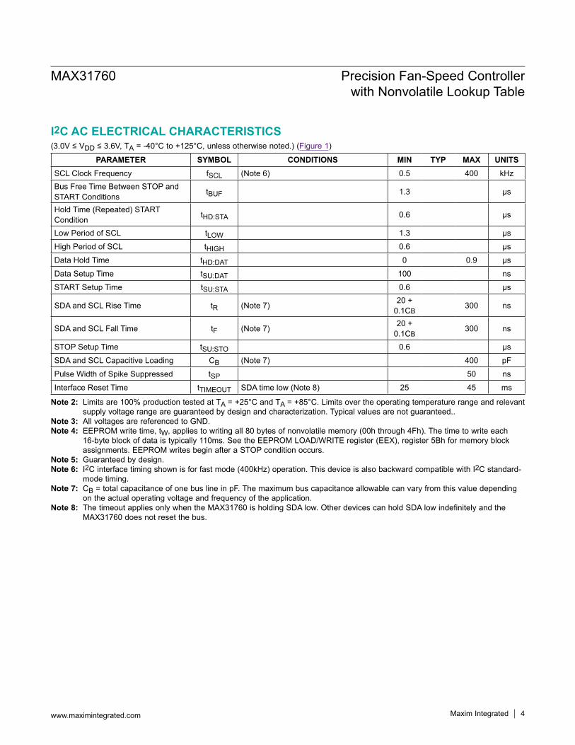
I2C AC ELECTRICAL CHARACTERISTICS(3.0V ≤ VDD ≤ 3.6V, TA = -40°C to +125°C, unless otherwise noted.) (Figure 1)
Note 2: Limits are 100% production tested at TA = +25°C and TA = +85°C. Limits over the operating temperature range and relevant supply voltage range are guaranteed by design and characterization. Typical values are not guaranteed..
Note 3: All voltages are referenced to GND.Note 4: EEPROM write time, tW, applies to writing all 80 bytes of nonvolatile memory (00h through 4Fh). The time to write each
16-byte block of data is typically 110ms. See the EEPROM LOAD/WRITE register (EEX), register 5Bh for memory block assignments. EEPROM writes begin after a STOP condition occurs.
Note 5: Guaranteed by design.Note 6: I2C interface timing shown is for fast mode (400kHz) operation. This device is also backward compatible with I2C standard-
mode timing.Note 7: CB = total capacitance of one bus line in pF. The maximum bus capacitance allowable can vary from this value depending
on the actual operating voltage and frequency of the application.Note 8: The timeout applies only when the MAX31760 is holding SDA low. Other devices can hold SDA low indefinitely and the
MAX31760 does not reset the bus.
PARAMETER SYMBOL CONDITIONS MIN TYP MAX UNITSSCL Clock Frequency fSCL (Note 6) 0.5 400 kHzBus Free Time Between STOP and START Conditions tBUF 1.3 µs
Hold Time (Repeated) START Condition tHD:STA 0.6 µs
Low Period of SCL tLOW 1.3 µs
High Period of SCL tHIGH 0.6 µs
Data Hold Time tHD:DAT 0 0.9 µs
Data Setup Time tSU:DAT 100 ns
START Setup Time tSU:STA 0.6 µs
SDA and SCL Rise Time tR (Note 7) 20 + 0.1CB
300 ns
SDA and SCL Fall Time tF (Note 7) 20 + 0.1CB
300 ns
STOP Setup Time tSU:STO 0.6 µs
SDA and SCL Capacitive Loading CB (Note 7) 400 pF
Pulse Width of Spike Suppressed tSP 50 ns
Interface Reset Time tTIMEOUT SDA time low (Note 8) 25 45 ms
MAX31760 Precision Fan-Speed Controller with Nonvolatile Lookup Table
www.maximintegrated.com Maxim Integrated │ 4

Typical Operating Characteristics(3.0V ≤ VDD ≤ 3.6V, unless otherwise noted.)
2000
2200
2400
2600
2800
3000
3200
3400
-40 10 60 110
ACTI
VE C
URRE
NT (m
A)
TEMPERATURE (°C)
ACTIVE CURRENT vs TEMPERATUREtoc01
1500
1600
1700
1800
1900
2000
2100
2200
2300
2400
2500
-40 10 60 110
STAN
DBY
CURR
ENT
(mA)
TEMPERATURE (°C)
STANDBY CURRENT vs TEMPERATUREtoc02
-4
-3
-2
-1
0
1
2
3
4
-40 -15 10 35 60 85 110
INTE
RNAL
TEM
PRAT
URE
ERRO
R (°C
)
TEMPERATURE (°C)
INTERNAL TEMPERATURE ERROR vs TEMPERATURE
toc03
VDD = 3.3V
Figure 1. I2C Timing Diagram
SCL
NOTE: TIMING IS REFERENCED TO VIL(MAX) AND VIH(MIN).
SDA
STOP START REPEATEDSTART
tBUF
tHD:STA
tHD:DAT tSU:DAT
tSU:STO
tHD:STAtSP
tSU:STAtHIGH
tR
tFtLOW
MAX31760 Precision Fan-Speed Controller with Nonvolatile Lookup Table
www.maximintegrated.com Maxim Integrated │ 5

PIN NAME FUNCTION1 DXP Analog Current Output/Voltage Input. Connect to the anode of the remote diode.
2 DXN Analog Input. Connect to the cathode of the remote diode. Do not connect to ground.
3 A0
Address Select Input. Determines I2C slave address. Must be connected to VDD or GND.4 A1
5 A2
6 PWM PWM Output. Open-drain output for fan drive. The power-on default for this pin is high impedance.
7 TACH1 Tachometer Input 1. Logic input for measuring speed of fan 1.
8 GND Ground Connection
9 TACH2 Tachometer Input 2. Logic input for measuring speed of fan 2.
10 N.C. No Connection. Not internally connected.
11 SHDN Active-Low Shutdown Output. Open-drain output for system shutdown when overtemperature is detected. Requires a pullup resistor. High impedance when VDD = 0V.
12 FF/FSActive-Low Fan-Failure Output and Full-Speed Input (Open Drain).The device pulls this output low if a fan failure is detected. The fan is forced to run full speed if this pin is pulled low externally. A pullup resistor to VDD is recommended.
13 ALERT Active-Low Alert Output. Open-drain fault output. ALERT is triggered when a measured temperature ex-ceeds its programmed high limit. A pullup resistor to VDD is recommended.
14 SDA Serial Data Input/Output. Input/Output for I2C data.
15 SCL Serial Clock Input. Input for I2C clock.
16 VDD Power-Supply Input. 3.0V to 3.6V voltage supply.
16
15
14
13
12
11
10
9
1
2
3
4
5
6
7
8
VDD
SCL
SDA
ALERT
FF/FS
SHDN
N.C.
TACH2
TOP VIEW
QSOP
DXN
DXP
A0
PWM
A1
A2
TACH1
GND
+
MAX31760
Pin Configuration
Pin Description
MAX31760 Precision Fan-Speed Controller with Nonvolatile Lookup Table
www.maximintegrated.com Maxim Integrated │ 6

Detailed DescriptionThe MAX31760 is a precision lookup table (LUT)-based PWM fan controller. The device accurately measures its internal die temperature and the temperature of an exter-nal diode-connected transistor, which can be a discrete small-signal device like a 2N3906 or a thermal diode on the die of a CPU, graphics processor unit (GPU), or other ASIC. Fan speed is controlled based on the temperature reading as an index to a 48-byte nonvolatile LUT contain-ing user-programmed PWM values. The temperature read-ing that is used as an index to the LUT can be either the local value, the remote value, or the greater of these two. The PWM values selected from the LUT determine the duty cycle of the PWM, which can be used to drive 4-wire, 3-wire, or 2-wire fans. The flexible LUT-based architecture enables the user to program a smooth nonlinear fan speed
vs. temperature transfer function often desired to minimize acoustic fan noise. All fan-control profile and configuration settings can be stored in nonvolatile memory that loads into operating memory at power-up or on request, allowing automatic, independent fan speed control.In addition to using temperature measurements to deter-mine PWM duty cycle, the device also features multiple temperature thresholds for thermal protection. The tem-perature thresholds include local high set point (LHS), local overtemperature set point (LOTS), remote high set point (RHS), and remote overtemperature set point (ROTS). These thresholds are programmable through the I2C-compatible interface. ALERT is pulled low to indicate a temperature fault state if the local temperature exceeds the LHS or remote temperature exceeds the RHS.
I2CINTERFACE
TEMPSENSOR
CONTROLLOGIC/
REGISTERS
LUTADDRESSREGISTER
PWM GENERATOR
ADC
TACHOMETERDETECTION
INTERNALDIODE
VDD
GND
SDA
SCL
DXP
DXN
PWM
ALERT
MAX31760
TACH2
TACH1
6.4MHzOSCILLATOR
1/758; 1/167; 1/17; 1/1
1/64
MUX
A0/A1/A2
SHDN
FF/FS
VDD
TEMPERATURE ALERT
OVER-TEMPERATURE SHUTDOWN
FULL SPEED INPUT
FAN FAIL OUTPUT
TEMP
48 BYTELOOKUPTABLE(LUT)
EEPROM
Block Diagram
MAX31760 Precision Fan-Speed Controller with Nonvolatile Lookup Table
www.maximintegrated.com Maxim Integrated │ 7

If LOTS or ROTS is surpassed, SHDN is pulled low to shut down the system in order to avoid thermal damage.The device has two TACH input pins, TACH1 and TACH2, that can accept the tachometer outputs from two 4-wire or 3-wire fans, thereby allowing them to monitor RPM and detect faults for both fans. If the fans generate “locked rotor” or “rotation detector” (RD) signals rather than tachometer pulses, TACH1 and TACH2 can be configured to read the RD signals and detect whether a fan has stopped rotat-ing. Based on the inputs at the TACH pins, the device can detect if a fan fault has occurred. If a fan fault is detected, FF/FS is pulled low and the PWM duty cycle is forced to the value selected in the FFDC register (03h).
Temperature SensingAn internal temperature sensor measures the die (local) temperature. The device also measures the temperature of a remote diode-connected transistor. The resolution is 0.125°C for both local and remote temperature sensing. Each temperature reading is represented by an 11-bit, two’s complement word that contains 10 bits of magnitude data and one sign bit. The value of the least significant bit (LSB), bit 5, is 0.125°C. The temperature data format is left-aligned with the sign at bit 15. Table 1 and Table 2 shows the temperature data register format.The remote temperature reading is stored in the remote temperature registers, with the MSB portion in the high Remote Temperature Reading register (RTH) and the
LSB portion in the low Remote Temperature Reading register (RTL). The local temperature reading is stored in the local temperature registers, with the MSB portion in the high Local Temperature Reading register (LTH) and the LSB portion in the low Local Temperature Reading register (LTL).
Temperature-Sensing Diode Ideality Factor CorrectionThe diode ideality factor, nd, plays an important role in the measurement of temperature in an external diode-connected transistor (or thermal diode). The value of nd is process-dependent and varies between devices. If the temperature measurement algorithm assumes the temperature-sensing diode’s ideality factor is nASSUMED but the actual value is nREAL, an error is incurred by this ideality factor mismatch:TERROR = TMEASURED - TREAL = (nREAL/nASSUMED - 1)
x TREALTo use an ideality factor close to the actual value, the device provides an ideality factor LUT. There are 64 pre-selected ideality factors in the table. Select the ideality factor value to be used in temperature sensing by setting the Ideality Factor register (IFR) to the value closest to the actual ideality of the sensing diode to be used. Table 3 shows the IFR bitmap and Table 4 shows the ideality fac-tor LUT. The device’s factory-programmed default ideality factor is 1.008 (position 18h).
Table 1. Temperature Data Format
Table 2. Temperature Reading Examples
TEMPERATURE DATA FORMAT: REMOTE AND LOCAL (°C)HIGH REGISTER BITS LOW REGISTER BITS
15 14 13 12 11 10 9 8 7 6 5 4 3 2 1 0Sign 64 32 16 8 4 2 1 0.5 0.25 0.125 0 0 0 0 0
TEMPERATURE (°C)REGISTER VALUES IN BINARY REGISTER VALUES IN HEX
HIGH REGISTER LOW REGISTER HIGH REGISTER LOW REGISTER+125 0111 1101 0000 0000 7Dh 00h+85 0101 0101 0000 0000 55h 00h+25 0001 1001 0000 0000 19h 00h+1 0000 0001 0000 0000 01h 00h
+0.125 0000 0000 0010 0000 00h 20h0 0000 0000 0000 0000 00h 00h
-0.125 1111 1111 1110 0000 FFh E0h-1 1111 1111 0000 0000 FFh 00h
-25 1110 0111 0000 0000 E7h 00h-55 1100 1001 0000 0000 C9h 00h
MAX31760 Precision Fan-Speed Controller with Nonvolatile Lookup Table
www.maximintegrated.com Maxim Integrated │ 8

Table 3. Ideality Factor Register (IFR)
Table 4. Transistor Ideality Register
Table 5. Temperature Threshold Registers
ADDRESS BIT 7 BIT 6 BIT 5 BIT 4 BIT 3 BIT 2 BIT 1 BIT 005h 0 0 IF5 IF4 IF3 IF2 IF1 IF0
SELECTION (HEX)
IDEALITY FACTOR
SELECTION (HEX)
IDEALITY FACTOR
SELECTION (HEX)
IDEALITY FACTOR
0x00 0.9844 0x16 1.0060 0x2C 1.02860x01 0.9853 0x17 1.0070 0x2D 1.02960x02 0.9863 0x18 1.0080 0x2E 1.03070x03 0.9873 0x19 1.0090 0x2F 1.03170x04 0.9882 0x1A 1.0100 0x30 1.03280x05 0.9892 0x1B 1.0110 0x31 1.03380x06 0.9902 0x1C 1.0120 0x32 1.03490x07 0.9911 0x1D 1.0130 0x33 1.03600x08 0.9921 0x1E 1.0141 0x34 1.03700x09 0.9931 0x1F 1.0151 0x35 1.03810x0A 0.9941 0x20 1.0161 0x36 1.03920x0B 0.9950 0x21 1.0171 0x37 1.04020x0C 0.9960 0x22 1.0182 0x38 1.04130x0D 0.9970 0x23 1.0192 0x39 1.04240x0E 0.9980 0x24 1.0202 0x3A 1.04350x0F 0.9990 0x25 1.0213 0x3B 1.04450x10 1.0000 0x26 1.0223 0x3C 1.04560x11 1.0010 0x27 1.0233 0x3D 1.04670x12 1.0020 0x28 1.0244 0x3E 1.04780x13 1.0030 0x29 1.0254 0x3F 1.04890x14 1.0040 0x2A 1.0265 ≥0x40 Not Valid0x15 1.0050 0x2B 1.0275 — —
TEMPERATURE THRESHOLDSREGISTERS
HIGH BYTE (MSB) LOW BYTE (LSB)Local High Set Point (LHS) LHSH (0Ch) LHSL (0Dh)Remote High Set Point (RHS) RHSH (06h) RHSL (07h)Local Overtemperature Set Point (LOTS) LOTSH (08h) LOTSL (09h)Remote Overtemperature Set Point (ROTS) ROTSH (0Ah) ROTSL (0Bh)
MAX31760 Precision Fan-Speed Controller with Nonvolatile Lookup Table
www.maximintegrated.com Maxim Integrated │ 9

Temperature ThresholdsThe device has four temperature thresholds: local high set point (LHS), remote high set point (RHS), local overtem-perature set point (LOTS), and remote overtemperature set point (ROTS). These thresholds are programmable and their data format is the same as the temperature readings shown in Table 1. Table 5 shows the registers that store the programmable temperature thresholds. When the measured temperature is greater than the cor-responding high set point, the open-drain ALERT output asserts low. When the measured temperature is greater than the corresponding overtemperature set point, the SHDN output asserts low.
Fan-Speed ControlPWM Fan-Speed ControlThe device’s open-drain PWM output is used to control the speed of one or two fans simultaneously. Furthermore, the device can be used to control 3-wire or 4-wire fans, and controls fan speed by varying the PWM duty cycle.
4-Wire Fan ControlA 4-wire fan has an input that can accept the speed-control signal from the PWM output. 25kHz, 1.5kHz, and 150Hz, PWM frequencies are available. The 25kHz frequency should be used for 4-wire fans, unless the fan manufacturer recommends otherwise. See Figure 2a.
3-Wire Fan ControlA 3-wire fan does not have an input for PWM control. External circuitry is needed to use the PWM output. There are two common ways to drive a 3-wire fan: supply modulation and variable DC drive. In the supply modulation approach, the fan supply voltage is modulated by the PWM signal and the fan speed is controlled by the PWM duty cycle. The typical PWM frequency for this mode is 33Hz (see Figure 2b). Another approach to 3-wire fan driving is to use the PWM signal to control a variable DC supply and this DC supply drives the fan continuously to realize speed control. The variable DC supply can be either a switching mode power supply (SMPS) or a low-cost LDO (such as the PQ20RX05/PQ20RX11), whose feedback is controlled by the filtered PWM (see Figure 2c).Direct PWM of the power supply has some important drawbacks. First, each rising or falling edge of the power supply waveform induces an audible noise transient from the fan. Second, when the supply modulation technique is used to drive a 3-wire fan, the tachometer signal is also
Figure 2a. Speed Control Using Fan’s PWM Input (4-Wire Fan)
Figure 2b. PWM Supply Modulation (3-Wire Fan)
Figure 2c. LDO Regulator Control (3-Wire Fan Driven by Variable Switching Mode Power Supply (SMPS) or LDO Regulator)
MAX31760
4-WIRE FAN
TACH
PWM
TACH1
PWM
RPU_TACHRPU_PWMVDD
+3.3V
PWM FREQUENCY 25kHz, DRV = 11
GND GND
VCC
FAN VOLTAGE
MAX31760
3-WIRE FAN
TACHTACH1
PWM
RPU_TACHRPU_PWMVDD
+3.3VPWM FREQUENCY 33Hz, DRV = 00
GND GND
PWM
VCC
FAN VOLTAGE
MAX31760
3-WIRE FAN
TACHTACH1
PWM
RPU_TACHVDD
SMPS OR LDOREGULATOR
+3.3V
GND GND
VCC
FB
VOUT
VIN
PWM FREQUENCY 25kHz, DRV = 11
MAX31760 Precision Fan-Speed Controller with Nonvolatile Lookup Table
www.maximintegrated.com Maxim Integrated │ 10

modulated by the PWM signal. During the “off” period of the waveform, there is no TACH signal. If the “on” period is sufficiently long (relative to the TACH period) so that four TACH periods are available, then fan speed can be measured and fan failure can be detected. If the “on” peri-od is too short, a full TACH period may not be available, which prevents the fan’s speed from being measured. One approach to measuring fan speed when the nominal “on” period is too short (or the TACH periods are too long) is to insert a PWM pulse with extended on-time (pulse stretching) to measure four full tachometer periods. When pulse stretching is enabled and PWM polarity is positive (as selected by CR1.2), PWM will remain high until four TACH pulses have been counted. Figure 3 illustrates the idea of pulse stretching. If a full count is reached before counting four pulses, PWM will go low. (Note that if the PWM polarity is negative the stretched pulse will be low.) If fewer than 4 TACH periods are available, the stretched PWM pulse will have a nominal width equal to a full count of (65535 x 4)/100kHz = 2.62s. Note that while pulse stretching is enabled, the fan fault detection will take place during “normal” PWM pulses (between the stretched pulses) as well, but to avoid invalid fault detections, a fault will be detected only when 4 TACH periods have been counted. The PSEN bit (pulse stretch enable: CR3.2) enables pulse stretching. When enabled, a stretched pulse will occur approximately every 12s. Note that pulse stretching
can be enabled only when the PWM frequency is 33Hz (DRV = 00) and when TACHFULL = 0. If DRV≠0 or if TACHFUL = 1, the PSEN bit is ignored and pulse stretch-ing is disabled. If DRV is 00 and PSEN is 0, there is no pulse stretching. Under this condition, the TACH measurements are valid if PWM is sufficiently wide to allow 4 TACH pulses. This will typically be the case only with higher speed fans (e.g. 10,000RPM or greater). Another alternative to pulse stretching is to use the TACHFULL bit. If TACHFULL (CR3.3) is set to 1, TACH measurements will be valid only when the PWM duty cycle is 100%; if the duty cycle is not 100 % fan fault detection is disabled. Fan fault detection in this mode will therefore be active only part of the time (when the duty cycle is 100%), so the detection of fan faults may be relatively infrequent. When DRV is 00, TACHFULL is 0, and PSEN is 1, pulse stretching is enabled immediately after PSEN is set to 1. The next pulse is stretched to allow the device to obtain an accurate tachometer reading and update the TACH count register. Once the TACHx count register has been updated, normal PWM pulse output resumes. If PSEN is kept as 1, a stretched pulse is inserted into PWM pulse train once every 12s to avoid excessive audible noise. If a system only needs a TACH reading infrequently, the host can set PSEN to 1 when it needs the TACH update. After that, the host can clear PSEN to 0 and thus disable the
Figure 3. Pulse Stretching to Process TACH Information
PWM
IDEALTACH
TACH
PULSE
MAX31760 Precision Fan-Speed Controller with Nonvolatile Lookup Table
www.maximintegrated.com Maxim Integrated │ 11

pulse stretching. Doing so helps to minimize the audible noise introduced by pulse stretching. When the PWM frequency is 33Hz and the duty cycle is 0% or decreasing toward 0%, then fan fault detection is disabled. Also, when the PWM frequency is 33Hz, the FF_0 bit functionality (CR3.6) is not valid.
Variable DC Control Because pulse stretching can cause the fan to speed up in response to the longer pulse, this further increases the audible noise level associated with PWM of the power supply. In contrast, the variable DC drive approach keeps the fan continuously on, so the tachometer signal is not altered. One such approach, using either a linear or a switching regulator, is shown in Figure 2c.
PWM PolaritySet the active level of the PWM output using the PPS bit (PWM polarity: CR1.2). When PPS is 0, a 100% PWM output is high. When PPS is 1, a 100% PWM output is low.
Automatic Fan-Speed Control Based on LUTThe device uses a 48-byte LUT to map the measured temperature to a desired PWM duty cycle that controls fan speed. The local temperature, the remote temperature, or the larger of the two can be used as an index to the LUT. Control bits TIS (temperature index source: CR1.0) and MTI (maximum temperature as index: CR1.1) determine the source of the index. Table 6 shows the control bit val-ues and the corresponding temperature source.The factory-programmed default value is 1 for the TIS bit and 0 for the MTI bit. The PWM duty-cycle values in the
LUT are programmable through the I2C-compatible inter-face. Table 7 shows the 48-byte LUT.
LUT HysteresisThe device provides a programmable hysteresis for the LUT to prevent the duty cycle from alternating between two values if the measured temperature falls on the boundary between two windows. Figure 4 illustrates the LUT hysteresis, and Table 8 shows the HYST (LUT hys-teresis: CR1.5) control bit function.
Setting PWM Frequency and Duty CycleIn most 4-wire fan applications, set the PWM frequency to 25kHz as recommended by most fan manufacturers (150Hz and 1500Hz PWM frequencies are also available for fans that require them.) An internal 6.4MHz PWM clock generates PWM pulses. The PWM duty-cycle resolution is 1/256, so any available duty cycle can be represented by an 8-bit value in either a PWM duty-cycle register in the LUT, or the Direct Duty-Cycle Control register (PWMR) in memory location 50h.
PWM_Resolution = 1/256PWM_Duty_Cycle = PWM_Resolution x
PWM_Register_Value x 100Table 9 shows a few examples of register values and the corresponding duty cycles.For 1500Hz, 150Hz, or 33Hz PWM, the PWM clock fre-quency is divided by 17, 167, or 758 to yield the correct PWM frequency while maintaining 8-bit duty cycle resolu-tion. Table 10 summarizes common fan types and driving approaches.
Table 7. 48-Step I2C Programmable LUT Map
Table 6. Temperature Index Source
REGISTER NAME ADDRESS (HEX)LUT0 PWM value for T < +18°C 20hLUT1 PWM value for +18°C ≤ T < +20°C 21hLUT2 PWM value for +20°C ≤ T < +22°C 22h. . . . . . . . .
LUT45 PWM value for +106°C ≤ T < +108°C 4DhLUT46 PWM value for +108°C ≤ T < +110°C 4EhLUT47 PWM value for T ≥ +110°C 4Fh
MTI (CR1.1) TIS (CR1.0) TEMPERATURE INDEX SOURCE0 0 Local temperature is used as the index.0 1 Remote temperature is used as the index (factory default setting).1 X The maximum of the local temperature and the remote temperature is used as the index.
MAX31760 Precision Fan-Speed Controller with Nonvolatile Lookup Table
www.maximintegrated.com Maxim Integrated │ 12

Table 8. HYST Bit Hysteresis
Figure 4. LUT Hysteresis; HYST Bit (CR1.5) = 0
Table 9. PWM Duty Cycle and Register Value (PWMR, Register 50h)
HYST (CR1.5) HYSTERESIS (°C)0 21 4
REGISTER VALUE (HEX) PWM DUTY CYCLE (%)00h 0.0001h 0.3902h 0.78. . . . . .FDh 98.83FEh 99.22FFh Forced to 100.00
Table 10. Fan Type and Driving Modes
FAN CONTROL METHOD
PWM FREQUENCY
PWM CLOCK FREQUENCY
DUTY-CYCLE RESOLUTION
FAN SUPPLY
VOLTAGETACHOMETER SIGNAL CONTROL
BITS
4-wire fan 25kHz, 1.5kHz, 150Hz
6.4MHz, 376.47kHz, 38.32kHz
1/256 Constant magnitude Standard
DRV = 01, 10, or 11,
PSEN = don’t care
TACHFULL=0
3-wire fan driven by
variable DC supply
25kHz 6.4MHz 1/256 Variable magnitude
Standard as long as the fan supply voltage
is greater than the minimum value for the fan’s internal circuitry.
DRV =11,PSEN = don’t
careTACHFULL=0
3-wire fan driven by supply
modulation (pulse stretching
enabled)
33Hz 8.3kHz 1/256
Pulse-width modulated
(can create audible noise)
Modulated by PWM. Measured during
periodic stretched PWM pulses. Stretched pulses
may cause audible artifacts with some fans.
DRV = 00,PSEN = 1
TACHFULL=0
3-wire fan driven by supply
modulation (pulse stretching
disabled)
33Hz 8.3kHz 1/256 Pulse-width modulated
Modulated by PWM. Measured only when duty cycle is 100%.
DRV = 00,PSEN = 0
TACHFULL=1
DECREASINGTEMPERATURE
INCREASINGTEMPERATURE
18
LUT5
LUT4
LUT3
LUT2
LUT1
22 26 30 34 38TEMPERATURE (°C)
MEMO
RY LO
CATI
ON
HYSTERESISWINDOW
MAX31760 Precision Fan-Speed Controller with Nonvolatile Lookup Table
www.maximintegrated.com Maxim Integrated │ 13

Direct (“Manual”) Fan-Speed ControlIf desired, the LUT can be overridden and the master can control the fan speed directly by writing a PWM duty-cycle value to PWMR (Register 50h). Table 9 shows the relationship between the value written to PWMR and the PWM duty cycle.To activate direct fan-speed control (thus disabling the LUT functionality), set control bit DFC (direct fan control, CR2.0) to 1. Then write the desired PWM duty-cycle value to the PWMR register. Clearing control bit DFC disables direct fan-speed control, and the LUT is automatically selected to control the fan speed based on the measured temperature value(s).
PWM Duty-Cycle Ramp RateTo ensure minimal audibility of fan-speed variations as temperature and PWM duty cycles change, the device changes the output PWM duty cycle at a selectable rate (determined by the RAMP0 and RAMP1 bits in Control Register 3) to minimize the rate at which the fan’s acous-tic noise increases and decreases (Table 11). This ramp rate applies for both LUT-based fan-speed control and direct fan-speed control.The PWM duty cycle always ramps toward the latest target value determined by the LUT. For example, if the temperature rises to +30°C, the duty cycle begins ramp-ing toward the value corresponding to +30°C in the LUT (D30). If the temperature drops to +24°C before duty cycle D30 has been reached, the target duty cycle is now D24, and the duty cycle begins moving toward D24 (the
duty-cycle setting corresponding to the LUT register for +24°C).During the ramp-up process, the actual output PWM duty cycle is not same as the target value. The PWMV register stores the current value of the PWM duty-cycle setting.Read PWMV (Register 51h) to obtain the current PWM duty cycle.
Fan Spin-UpSome fans cannot reliably start spinning from a stopped condition unless driven with close to 100% duty cycle (or supply voltage, in the case of 3-wire fans). To overcome this problem, an optional fan spin-up function can be enabled to start the fan reliably. Spin-up overcomes the fan’s inertia by providing it with 100% drive for a short time. If spin-up is enabled, changing the selected duty cycle from zero to a nonzero value causes the PWM duty cycle to immediately go to 100% until one of the following conditions is met, whichever comes sooner:• A 2s timeout has passed, or• Two tachometer pulses are detected at each enabled
TACH inputAfter the spin-up period is over, the PWM duty cycle reverts to the value determined by the LUT or the value in the PWMR register, depending on the status of the DFC bit (direct fan control: CR2.0). If spin-up is disabled, the PWM duty cycle is always determined by the output of the LUT or the direct fan control register, depending on the state of the DFC bit. Enable fan spin-up by setting the SPEN bit (spin-up enable: CR2.5) to 1.
Table 11. PWM Duty-Cycle Ramp Rates
RAMP1 RAMP0 PWM ADJUST RAMP RATE SELECT PWM DUTY-CYCLE CHANGE ALLOWED PER SECOND (%)
0 0 Slow (default) 3.1250 1 Slow-Medium 6.251 0 Medium-Fast 12.51 1 Fast Immediate
MAX31760 Precision Fan-Speed Controller with Nonvolatile Lookup Table
www.maximintegrated.com Maxim Integrated │ 14
Tachometer InputsThe device has two TACH input pins, TACH1 and TACH2, that accept the tachometer signals from two fans inde-pendently. Tachometer signals are typically open drain so external pullup resistors are needed for the TACH1 and TACH2 pins. TACH1, TACH2, or both can be dis-abled depending on the number of fans that need to be monitored. The tachometer enable bits, TACH1E (CR3.0) and TACH2E (CR3.1), control the enabling/disabling of TACH1 and TACH2, respectively. To enable a fan-monitoring input, set the enable/disable bit for that input to 1. Both TACH inputs are factory programmed to default enabled.The speed of each fan can be determined using the con-tents of the TACH count registers. There is an internal fan-counter clock running at 100kHz. To cancel out the effect of the mechanical tolerance, the device counts the number of fan-counter clock periods over four tachometer pulses. The resulting average tachometer pulse count is stored in a 2-byte TACH count register. Table 12 shows the register definitions.If the decimal value in TCxH is {TCxH} and the decimal value in TCxL is {TCxL}, where x = 1 or 2, the RPM of the fan can be calculated as:
Fan_RPM = 60 x 100,000/({TCxH} x 256 + {TCxL}/nwhere n is the number of pulses generated by the tachometer per revolution.To detect fan failure, write a TACH count failure threshold value in the 2-byte TACH Count Threshold register (TCTH and TCTL). When the values in the TACH_ Count register pairs are higher than the value in the threshold register pair, or when overflow occurs, the fan is considered as running at a speed lower than the threshold and the fan-fault error is indicated in the Status register and (if not masked) with the FF_FS output. During the first 2s of fan startup, fan-error detection is disabled, whether or not spin-up is enabled. After 2s, fan-error detection is enabled to ensure reliable fan monitoring. Fan-failure detection is disabled when the PWM duty cycle is zero or decreasing to zero.
Care must be taken when counting the tachometer output from a 3-wire fan driven by power-supply modulation. See the PWM Fan-Speed Control section for more information.Some 3-wire fans provide a “rotation detection” (RD) or “locked rotor” signal that indicates whether or not the fan is running. When the FSST bit (fan-sense signal type: CR2.1) is set to 1, TACH1 and TACH2 are configured to accept RD signals instead of TACH signals. The polarity of the RD signal is selectable. If the RDPS bit (rotation-detection signal-polarity selection: CR2.2) is set to 1, the device interprets RD high, as indicating that the fan is spinning. If RDPS is cleared to 0, the device interprets RD low, as indicating that the fan is spinning. If the RD signal at either TACH1 or TACH2 indicates the fan is stalled, a fan-fault error is detected, except when bit 6 of CR3 is set to 0 and the PWM duty cycle is zero or is ramping down to a target value of zero.When a fan-fault error is detected three times in a row (see the Fault Queue section for more information), FF/FS is asserted low and the PWM output duty cycle is forced to the value in register 03h. TACH signals are still monitored as long as a TACH input is enabled, and if the fan speed returns to the correct value, normal operation resumes .
Temperature Alert Output (ALERT)The device has an open-drain ALERT output to indicate that the measured temperature has extended beyond a temperature threshold. This output can be used as either a fault indicator or an interrupt output. In the fault indica-tor (comparator) mode, the ALERT asserts low when the local temperature exceeds LHS or the remote tem-perature exceeds RHS. When the temperature returns to the normal range, ALERT deasserts. A 1°C hysteresis is associated with the Local High and Remote High Alarms. To set the fault-indicator mode, set control bit ALERTS (ALERT functionality selection: CR2.6) to 1.The ALERT output can also be configured as an interrupt output. In this mode, the output asserts low when the local temperature exceeds LHS or the remote temperature exceeds RHS. The ALERT output remains asserted until it is cleared, even if the error condition is no longer pres-ent. In this mode, reading the Status register (SR, memo-
Table 12. TACH Count AddressesREGISTER MSB ADDRESS LSB ADDRESS
TACH1 Count (High/Low) TC1H 52h TC1L 53hTACH2 Count (High/Low) TC2H 54h TC2L 55h
MAX31760 Precision Fan-Speed Controller with Nonvolatile Lookup Table
www.maximintegrated.com Maxim Integrated │ 15

ry address 5Ah) sets the Alert Mask bit (ALTMSK - CR1.7) if LHA or RHA is set. This prevents further ALERT trigger-ing until the master clears the condition at the end of the interrupt service routine by writing a 0 to the ALTMSK bit (CR1.7). LHA and RHA are cleared by a read command from the master, and are reasserted at the end of next conversion if the triggering condition persists. The control bit ALERTS (CR2.6) must be written to a 0 for ALERT to be used as an interrupt output. This is the default factory-programmed state. The following sequence describes the response of a system that uses the ALERT output pin as an interrupt flag:1) Master senses ALERT low.2) Master reads the device SR register to determine what
caused the ALERT.3) The device clears LHA, RHA, LOTA, and ROTA, resets
the ALERT output pin back to high impedance, and sets the Alert Mask bit (CR1.7) to 1, masking new faults from asserting ALERT.
4) Master attends to conditions that caused ALERT to be triggered, for example, the fan is started, set point limits are adjusted, etc.
5) Master writes a 0 to the ALTMSK bit in CR1 to reset the interrupt.
Overtemperature Shutdown (SHDN)The SHDN pin is pulled low if the local temperature exceeds LOTS or the remote temperature exceeds ROTS. The LOTA bit (SR.4) is set to 1 if the local tem-perature exceeds LOTS. The ROTA bit (SR.2) is set to 1 if the remote temperature exceeds ROTS. SHDN can be used to prevent thermal damage by shutting down the system. A 10°C hysteresis is associated with the overtemperature detection. The ROTA bit is reset and the SHDN output deasserts (back to high impedance) when the remote temperature drops to or less than the ROTS value minus 10°C. The same hysteresis applies to local overtemperature detection. Reading the status register has no effect on either the SHDN output or the status bits ROTA and LOTA.
Fan-Fail Output and Full-Speed Input (FF/FS)FF/FS is a combination of fan-fail open-drain output and full-speed input. Two types of fan failure detection are supported, depending on the type of output signal avail-able from the fan. If the fan has a tachometer output that produces pulses (typically 2 per revolution) as the fan spins, failure is determined by determining the rate of the TACH pulses. If the fan has a failure detection output (often called a “locked rotor” output), failure is determined
by detecting the state of this output. The type of failure detection is selected by the FSST bit (CR2.1). Select FSST = 0 when the fan has a tachometer out-put. Most tachometer outputs provide two square-wave pulses per revolution. Fan speed is determined by count-ing the number of internal clock cycles that occur during four tachometer periods. To detect fan failure, write a TACH count failure threshold value in 2-byte TACH count Threshold register (TCTH and TCTL). When the values in the TACH_Count register pairs are higher than the value in the threshold register pair or when overflow occurs, the fan is considered as running at a speed lower than the threshold and a fan-fault error is generated. Three con-secutive detections will cause the FF/FS output to assert. Select FSST = 1 when the fan has a rotation detection (or “locked rotor”) output. If the fan’s rotation detection output is high when the fan is running, set the RDPS bit (CR2.2) to 1. Fan failure will cause the output to go low, driving the TACH input low and causing detection of a fan fault. Three consecutive detections of the low output will cause the FF/FS output to assert. If the fan’s rotation detection output is low when the fan is running, set the RDPS bit to 0, which will cause a fan fault to be detected when the TACH input is driven high. For the fault output to be asserted for either signal type, the fault must occur for three consecutive times. If the TACH alarms are not masked by bits 0:1 in Alert Mask registers, fan failure detection causes the FF/FS output to assert low. When a fan failure has been detected, the PWM duty cycle is forced immediately to the value in the FFDC register (03h). Many 4-wire fans stop spinning when the applied PWM duty cycle is zero. When such a fan is used, set bit FF_0 (CR3.6) to 0. This disables fan-failure detection when the PWM duty cycle is zero or ramping down to zero. This prevents detecting a fan failure when the fan is intended to be stopped. Some 4-wire fans are designed to continue spinning when the applied PWM duty cycle is zero. When such a fan is used, set bit FF_0 (CR3.6) to 1. This enables fan-failure detection for all values of duty cycle. For 3-wire fans operating from a PWM-modulated power supply, fan operation stops when the duty cycle is zero. Therefore, when the PWM frequency is set to 33Hz, fan fault detection is disabled when PWM duty is zero or decreasing to zero. The FF Mode bit (CR2.4) selects whether the FF/FS output operates in comparator mode or interrupt mode.
MAX31760 Precision Fan-Speed Controller with Nonvolatile Lookup Table
www.maximintegrated.com Maxim Integrated │ 16

In comparator mode, FF/FS asserts upon detection of failure and de-asserts if the fan subsequently begins to spin again. The status bits will remain set if the fan begins to spin again. Writing 1 to CLR_FAIL bit (CR3.7) clears the fan fail status bits (TACH1A and TACH2A). These bits will set again if a fan failure is subsequently detected. Bit CR3.7 self-clears to 0. In Interrupt mode, FF/FS asserts upon detection of failure and remains asserted until the status bits are cleared by writing 1 to CLR_FAIL bit. In either mode, FF/FS and fault status can be cleared by disabling TACH inputs. If FF/FS is pulled low externally by another device, and if the FS_ENABLE bit (CR2.3) is set to 1, the PWM duty cycle is forced to be 100%. An application for this feature is two devices that have their FF/FS pins connected together. If one device detects a fan failure and asserts its FF/FS pin, the FF/FS pin of the other device is also pulled low and therefore its PWM duty cycle is forced to 100% to compensate for the loss of cooling from the failed fans.
Fault QueueThe device features a “fault queue” to avoid false alarms. For a fault output (ALERT, FF/FS, or SHDN) to be trig-gered, the fault must occur three consecutive times. The fault sources include out-of-limit temperature readings and fan failures.
Standby ModeThe device features a standby mode to conserve power. In the standby mode, temperature sensing, tachometer
pulse counting, and PWM output are stopped. The I2C interface remains active during the standby. Set the STBY bit (standby mode enable: CR2.7) to 1 to enable the standby mode.
I2C Serial Interface DescriptionI2C DefinitionsThe following terminology is commonly used to describe I2C data transfers. See the I2C timing diagram (Figure 1) and the I2C AC Electrical Characteristics table for addi-tional information.Master Device: The master device controls the slave devices on the bus. The master device generates SCL clock pulses and START and STOP conditions.Slave Devices: Slave devices send and receive data at the master’s request.Bus Idle or Not Busy: Time between STOP and START conditions when both SDA and SCL are inactive and in their logic high states. A STOP condition is the proper method to return the bus to the idle state.START Condition: A START condition is generated by the master to initiate a new data transfer with a slave. Transitioning SDA from high to low while SCL remains high generates a START condition.STOP Condition: A STOP condition is generated by the master to end a data transfer with a slave. Transitioning SDA from low to high while SCL remains high generates a STOP condition.Repeated START Condition: The master can use a repeated START condition at the end of one data trans-fer to indicate that it will immediately initiate a new data transfer following the current one. Repeated STARTs are commonly used during read operations to identify a spe-cific memory address to begin a data transfer. A repeated START condition is issued identically as a normal START condition,Bit Write: Transitions of SDA must occur during the low state of SCL. The data on SDA must remain valid and unchanged during the entire high pulse of SCL plus the setup and hold time requirements. Data is shifted into the device during the rising edge of the SCL.Bit Read: At the end of a write operation, the master must release the SDA bus line for the proper amount of setup time before the next rising edge of SCL during a bit read. The device shifts out each bit of data on SDA at the falling edge of the previous SCL pulse and the data bit is valid at the rising edge of the current SCL pulse.
Figure 5. I2C Slave Address Byte
Table 13. Available I2C AddressesA2 A1 A0 SLAVE ADDRESS (HEX)0 0 0 A0h0 0 1 A2h0 1 0 A4h0 1 1 A6h1 0 0 A8h1 0 1 AAh1 1 0 ACh1 1 1 AEh
1 0 01 R/WA0A1A2MSB LSB
SLAVE ADDRESS*
*THE SLAVE ADDRESS IS DETERMINED BY ADDRESS PINS A0, A1, AND A2.
READ/WRITE BIT
MAX31760 Precision Fan-Speed Controller with Nonvolatile Lookup Table
www.maximintegrated.com Maxim Integrated │ 17
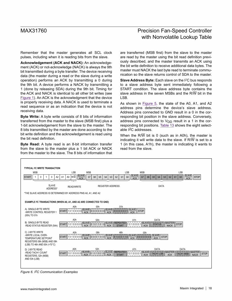
Remember that the master generates all SCL clock pulses, including when it is reading bits from the slave.Acknowledgement (ACK and NACK): An acknowledge-ment (ACK) or not-acknowledge (NACK) is always the 9th bit transmitted during a byte transfer. The device receiving data (the master during a read or the slave during a write operation) performs an ACK by transmitting a 0 during the 9th bit. A device performs a NACK by transmitting a 1 (done by releasing SDA) during the 9th bit. Timing for the ACK and NACK is identical to all other bit writes (see Figure 1). An ACK is the acknowledgment that the device is properly receiving data. A NACK is used to terminate a read sequence or as an indication that the device is not receiving data.Byte Write: A byte write consists of 8 bits of information transferred from the master to the slave (MSB first) plus a 1-bit acknowledgement from the slave to the master. The 8 bits transmitted by the master are done according to the bit write definition and the acknowledgement is read using the bit read definition.Byte Read: A byte read is an 8-bit information transfer from the slave to the master plus a 1 bit ACK or NACK from the master to the slave. The 8 bits of information that
are transferred (MSB first) from the slave to the master are read by the master using the bit read definition previ-ously described, and the master transmits an ACK using the bit write definition to receive additional data bytes. The master must NACK the last byte read to terminate commu-nication so the slave returns control of SDA to the master.Slave Address Byte: Each slave on the I2C bus responds to a slave address byte sent immediately following a START condition. The slave address byte contains the slave address in the seven MSBs and the R/W bit in the LSB.As shown in Figure 5, the state of the A0, A1, and A2 address pins determine the device’s slave address. Address pins connected to GND result in a 0 in the cor-responding bit position in the slave address. Conversely, address pins connected to VDD result in a 1 in the cor-responding bit positions. Table 13 shows the eight select-able I2C addresses.When the R/W bit is 0 (such as in A0h), the master is indicating it will write data to the slave. If R/W is set to a 1 (in this case, A1h), the master is indicating it wants to read from the slave.
Figure 6. I2C Communication Examples
SLAVEADDRESS*
START 1 0 1 0 A2 A1 A0 R/W SLAVEACK
MSB LSB
b7 b6 b5 b4 b3 b2 b1 b0
MSB LSB
READ/WRITE REGISTER ADDRESS
SLAVEACK b7 b6 b5 b4 b3 b2 b1 b0
MSB LSB
DATA
STOPSLAVEACK
A) SINGLE-BYTE WRITE-WRITE CONTROL REGISTER 1 (00h) TO 01h
B) SINGLE-BYTE READ-READ STATUS REGISTER (5Ah)
C) 2-BYTE WRITE-WRITE LOCAL OVER-TEMPERATURE SETPOINT REGISTERS 08h (MSB) AND 09h (LSB) TO 46h AND 00h (+70°C)
TYPICAL I2C WRITE TRANSACTION
START SLAVEACK
SLAVEACK STOP1 0 1 0 0 0 0 0 0 0 0 0 1 0 0 0
A0h 08h
START SLAVEACK
SLAVEACK
REPEATEDSTART
A1hSLAVE
ACKMASTER
NACK STOP1 0 1 0 0 0 0 0 0 1 0 1 1 0 1 05Ah
1 0 1 0 0 0 0 1
START SLAVEACK
SLAVEACK1 0 1 0 0 0 0 0 0 0 0 0 0 0 0 0
A0h 00hSLAVE
ACK STOP
STATUSDATA
46h
EXAMPLE I2C TRANSACTIONS (WHEN A0, A1, AND A2 ARE CONNECTED TO GND)
*THE SLAVE ADDRESS IS DETERMINED BY ADDRESS PINS A0, A1, AND A2
0 0 0 0 0 0 0 1
A0h
SLAVEACK
SLAVEACK
D) 2-BYTE READ-READ TACH1 COUNT REGISTERS, 52h (MSB) AND 53h (LSB)
START SLAVEACK STOP1 0 1 0 0 0 0 0 0 1 0 1 0 0 1 0
A0h 52hSLAVE
ACKREPEATED
START
A1hSLAVE
ACKMASTER
ACK1 0 1 0 0 0 0 1DATA
MASTERNACK
DATA
00h0 1 0 0 0 1 1 0 0 0 0 0 0 0 0 0
TACH1 MSBTACH1 LSB
01h
MAX31760 Precision Fan-Speed Controller with Nonvolatile Lookup Table
www.maximintegrated.com Maxim Integrated │ 18

If an incorrect (nonmatching) slave address is written, the device assumes the master is communicating with another I2C device and ignores the communication until the next START condition is sent.Memory Address: During an I2C write operation to the device, the master must transmit a memory address to identify the memory location where the slave is to store the data. The memory address is always the second byte transmitted during a write operation following the slave address byte.
I2C CommunicationSee Figure 6 for I2C communication examples.Writing a Single Byte to a Slave: The master must generate a START condition, write the slave address byte (R/W = 0), write the memory address, write the byte of data, and generate a STOP condition. The master must read the slave’s acknowledgement during all byte write operations.Writing Multiple Bytes to a Slave: To write multiple bytes to a slave, the master generates a START condi-tion, writes the slave address byte (R/W = 0), writes the memory address, writes up to 8 data bytes, and gener-ates a STOP condition. The device writes 1 to 8 bytes (one page or row) with a single write transaction. This is internally controlled by an address counter that allows data to be written to consecutive addresses without trans-mitting a memory address before each data byte is sent. The address counter limits the write to one 8-byte page (one row of the memory map). Attempts to write to addi-tional pages of memory without sending a STOP condition between pages results in the address counter wrapping around to the beginning of the present row. For example, a 3-byte write starts at address 06h and writes 3 data bytes (11h, 22h, and 33h) to three “consecu-tive” addresses. The result is that addresses 06h and 07h would contain 11h and 22h, respectively, and the third data byte, 33h, would be written to address 00h.To prevent address wrapping from occurring, the master must send a STOP condition at the end of the page, then wait for the bus-free or EEPROM write time to elapse. Then the master can generate a new START condition and write the slave address byte (R/W = 0) and the first memory address of the next memory row before continu-ing to write data.Acknowledge Polling: Any time a EEPROM byte is written, the device requires the EEPROM write time (tW) after the STOP condition to write the contents of the byte
to EEPROM. During the EEPROM write time, the device does not acknowledge its slave address because it is busy. It is possible to take advantage of this phenomenon by repeatedly addressing the device, which allows com-munication to continue as soon as the device is ready. The alternative to acknowledge polling is to wait for a maximum period of tW to elapse before attempting to access the device.Writing to and Loading from EEPROM: The contents of the EEPROM are loaded into the corresponding control registers on POR, and on command. Initiate a load from EEPROM by writing 1 to bit 7 of the EEX register (5Bh) and also to the bits corresponding to the register ranges to be loaded. To write to EEPROM, write 0 to bit 7 and to the bits corresponding to the register ranges to be written. EEX bits always auto-clear to 0. EEPROM Corruption and Recovery: Using the EEX register (5Bh), RAM can be written to EEPROM. If the power to the MAX31760 is interrupted during the EEPROM write cycle, there is a possibility that the data being written to the EEPROM will become corrupted. The MAX31760 can detect if this corruption has occurred, and will set the Program Corrupt bit (bit 7 of the Status Register; 5Ah) to a 1 to indicate that EEPROM corruption has been detected.To recover from this, make sure the RAM locations are filled with the desired values, then execute an EEPROM write cycle using the EEX register (5Bh), making sure that power is stable for the duration of the write cycle. Once complete, either power cycle the MAX31760 or set the Soft POR bit (bit 6 of CR1; register 00h). Once the power cycle is complete, read the Program Corrupt bit to confirm that it has returned a 0 value, indicating that the EEPROM has been properly stored.Reading a Single Byte from a Slave: Unlike the write operation that uses the specified memory address byte to define where the data is to be written, the read operation occurs at the present value of the memory address counter. To read a single byte from the slave, the master generates a START condition, writes the slave address byte with R/W = 1, reads the data byte with a NACK to indicate the end of the transfer, and generates a STOP condition. However, because requiring the master to keep track of the memory address counter is impractical, the next method should be used to perform reads from a specified memory location.Manipulating the Address Counter for Reads: A dummy write cycle can be used to force the address counter (or pointer) to a particular value. To do this, the master gen-
MAX31760 Precision Fan-Speed Controller with Nonvolatile Lookup Table
www.maximintegrated.com Maxim Integrated │ 19

erates a START condition, writes the slave address byte (R/W = 0), writes the memory address where it desires to read, generates a repeated START condition, writes the slave address byte (R/W = 1), reads data with ACK or NACK as applicable, and generates a STOP condition. Recall that the master must NACK the last byte to inform the slave that no additional bytes will be read.
Reading Multiple Bytes from a Slave: The read opera-tion can be used to read multiple bytes with a single transfer. When reading bytes from the slave, the master simply ACKs the data byte if it desires to read another byte before terminating the transaction. After the master reads the last byte it must NACK to indicate the end of the transfer and generates a STOP condition.
Register Memory Map
ADDRESS READ/WRITE NAME LOADED FROMEEPROM AT POR?
FACTORY DEFAULT FUNCTION
00h Read/Write CR1 Yes 01h Control Register 101h Read/Write CR2 Yes 10h Control Register 202h Read/Write CR3 Yes 03h Control Register 303h Read/Write FFDC Yes FFh Fan Fault Duty Cycle04h Read/Write MASK Yes C0h Alert Mask Register05h Read/Write IFR Yes 18h Ideality Factor Register06h Read/Write RHSH Yes 55h Remote High Set-point MSB07h Read/Write RHSL Yes 00h Remote High Set-point LSB08h Read/Write LOTSH Yes 55h Local Overtemperature Set-point MSB09h Read/Write LOTSL Yes 00h Local Overtemperature Set-point LSB0Ah Read/Write ROTSH Yes 6Eh Remote Overtemperature Set-point MSB0Bh Read/Write ROTSL Yes 00h Remote Overtemperature Set-point LSB0Ch Read/Write LHSH Yes 46h Local High Set-point MSB0Dh Read/Write LHSL Yes 00h Local High Set-point LSB0Eh Read/Write TCTH Yes FFh TACH Count Threshold Register, MSB0Fh Read/Write TCTL Yes FEh TACH Count Threshold Register, LSB
10h–17h Read/Write USER Yes 00h 8 Bytes of General-Purpose User Memory20h–4Fh Read/Write LUT Yes FFh 48-Byte Lookup Table (LUT)
50h Read/Write PWMR No 00h Direct Duty-Cycle Control Register51h Read Only PWMV No 00h Current PWM Duty-Cycle Register52h Read Only TC1H No 00h TACH1 Count Register, MSB53h Read Only TC1L No 00h TACH1 Count Register, LSB54h Read Only TC2H No 00h TACH2 Count Register, MSB55h Read Only TC2L No 00h TACH2 Count Register, LSB56h Read Only RTH No 00h Remote Temperature Reading Register, MSB57h Read Only RTL No 00h Remote Temperature Reading Register, LSB58h Read Only LTH No 00h Local Temperature Reading Register, MSB59h Read Only LTL No 00h Local Temperature Reading Register, LSB5Ah Read Only SR No 00h Status Register
5Bh Write Only EEX No 00h Load EEPROM to RAM; Write RAM to EEPROM
MAX31760 Precision Fan-Speed Controller with Nonvolatile Lookup Table
www.maximintegrated.com Maxim Integrated │ 20
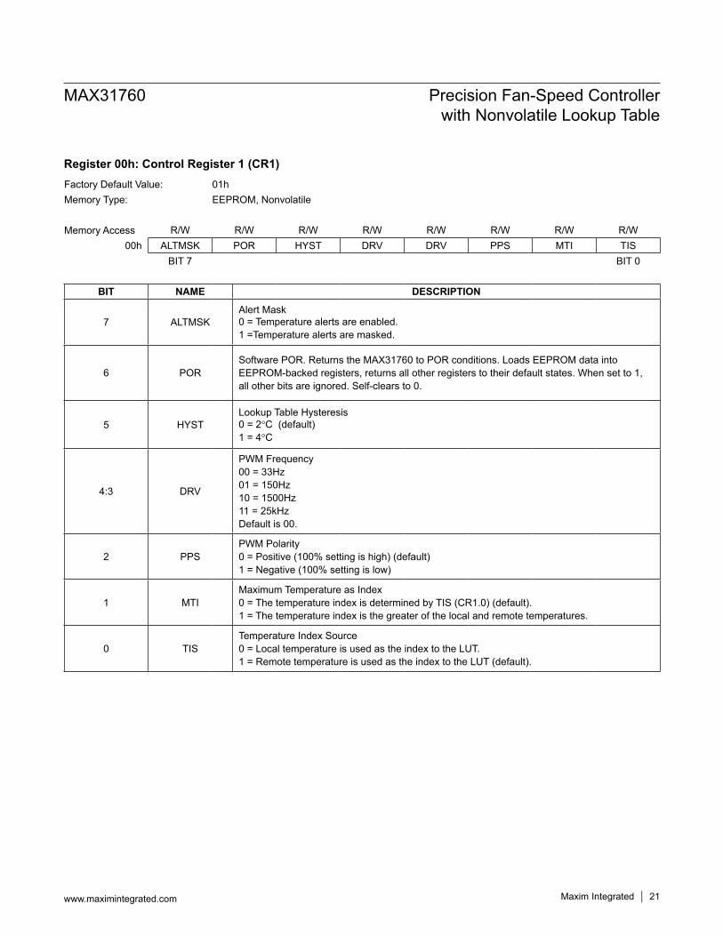
Register 00h: Control Register 1 (CR1)Factory Default Value: 01hMemory Type: EEPROM, Nonvolatile
Memory Access R/W R/W R/W R/W R/W R/W R/W R/W00h ALTMSK POR HYST DRV DRV PPS MTI TIS
BIT 7 BIT 0
BIT NAME DESCRIPTION
7 ALTMSKAlert Mask0 = Temperature alerts are enabled. 1 =Temperature alerts are masked.
6 PORSoftware POR. Returns the MAX31760 to POR conditions. Loads EEPROM data into EEPROM-backed registers, returns all other registers to their default states. When set to 1, all other bits are ignored. Self-clears to 0.
5 HYSTLookup Table Hysteresis0 = 2°C (default)1 = 4°C
4:3 DRV
PWM Frequency00 = 33Hz01 = 150Hz 10 = 1500Hz 11 = 25kHz Default is 00.
2 PPSPWM Polarity0 = Positive (100% setting is high) (default)1 = Negative (100% setting is low)
1 MTIMaximum Temperature as Index0 = The temperature index is determined by TIS (CR1.0) (default).1 = The temperature index is the greater of the local and remote temperatures.
0 TISTemperature Index Source0 = Local temperature is used as the index to the LUT.1 = Remote temperature is used as the index to the LUT (default).
MAX31760 Precision Fan-Speed Controller with Nonvolatile Lookup Table
www.maximintegrated.com Maxim Integrated │ 21

Register 01h: Control Register 2 (CR2)
Factory Default Value: 10h
Memory Type: EEPROM, Nonvolatile
Memory Access R/W R/W R/W R/W R/W R/W R/W R/W
01h STBY ALERTS SPEN FF Mode FS Enable RDPS FSST DFC
BIT 7 BIT 0
BIT NAME DESCRIPTION
7 STBYStandby Mode Enable0 = Normal operating mode (default).1 = Standby mode.
6 ALERTSALERT Functionality Selection0 = ALERT function as an interrupt (default).1 = ALERT functions as a “comparator mode” fault indicator.
5 SPENSpin-Up Enable0 = No spin-up when the fan starts up (default).1 = Spin-up enabled. The PWM duty cycle is 100% until the end criterion is met (default).
4 FF ModeFF Functionality Selection0 = FF/FS output functions as an interrupt.1 = FF/FS output functions as a “comparator mode” fault indicator (default).
3 FS EnableFS Input Enable0 = Externally driving FF/FS has no effect on duty cycle. (default).1 = Externally driving FF/FS low forces 100% duty cycle.
2 RDPS
Rotation-Detection (RD) Signal-Polarity Selection. This bit becomes irrelevant when the FSST = 0.0 = RD is at low level when the fan is running (default).1 = RD is at high level when the fan is running.
1 FSSTFan-Sense Signal Type0 = Fan tachometer provides square-wave pulses (default).1 = Fan provides rotation detection (RD) signal.
0 DFCDirect Fan Control (Manual Mode)0 = Direct fan control disabled (default).1 = Direct fan control enabled.
MAX31760 Precision Fan-Speed Controller with Nonvolatile Lookup Table
www.maximintegrated.com Maxim Integrated │ 22

Register 02h: Control Register 3 (CR3)Factory Default Value: 03hMemory Type: EEPROM, Nonvolatile
Memory Access R/W R/W R/W R/W R/W R/W R/W R/W02h CLR_FAIL FF_0 RAMP1 RAMP0 TACHFULL PSEN TACH2E TACH1E
BIT 7 BIT 0
BIT NAME DESCRIPTION
7 CLR_FAIL
Clear Fan Fail Status Bits 0 = Default; 1 = Clears any fan fail status bits to 0. Bits will be set again if failure is subsequently detected.
Clears FF/FS output if FF interrupt mode is selected. This bit self-clears to 0.
6 FF_00 Duty-Cycle Fan-Fail Detection 0 = Fan-fail detection disabled when duty cycle = 0 or when ramping toward 0 (default value). 1 = Fan-fail detection enabled for all duty-cycle values.
5:4 RAMP[1:0]
PWM Duty-Cycle Ramp Rate
RAMP1 RAMP0 PWM ADJUST RAMP RATE SELECT
PWM DUTY-CYCLE CHANGE PER SECOND (%)
0 0 Slow (default) 3.125 (default)0 1 Slow-Medium 6.251 0 Medium-Fast 12.51 1 Fast Immediate
3 TACHFULL 1 = Detect fan failure only when duty cycle =100%.
2 PSENPulse Stretch Enable. Applies only for 33Hz PWM.0 = Pulse stretch function is disabled (default).1 = Pulse stretch function is enabled.
1 TACH2ETACH2 Enable0 = TACH2 monitoring function is disabled. Clears TACH2 fan fail status bit and FF/FS output.1 = TACH2 monitoring function is enabled (default).
0 TACH1ETACH1 Enable0 = TACH1 monitoring function is disabled. Clears TACH1 fan fail status bit and FF/FS output.1 = TACH1 monitoring function is enabled (default).
MAX31760 Precision Fan-Speed Controller with Nonvolatile Lookup Table
www.maximintegrated.com Maxim Integrated │ 23

Register 03h: Fan Fault Duty Cycle (FFDC)Factory Default Value: FFhMemory Type:
Memory Access R/W R/W R/W R/W R/W R/W R/W R/W03h FFDC 7 FFDC 6 FFDC 5 FFDC 4 FFDC 3 FFDC 2 FFDC 1 FFDC 0
BIT 7 BIT 0
BIT NAME DESCRIPTION7 FFDC 7
FFDC [7:0] select the PWM duty cycle after a fan failure is detected per Table 9.
6 FFDC 6
5 FFDC 5
4 FFDC 4
3 FFDC 3
2 FFDC 2
1 FFDC 1
0 FFDC 0
MAX31760 Precision Fan-Speed Controller with Nonvolatile Lookup Table
www.maximintegrated.com Maxim Integrated │ 24

Register 04h: Alert Mask Register (MASK)
Register 05h: Ideality Factor Register (IFR)
Factory Default Value: C0hMemory Type: EEPROM, Nonvolatile
Memory Access N/A N/A R/W R/W R/W R/W R/W R/W04h Reserved Reserved LHAM LOTAM RHAM ROTAM TACH2AM TACH1AM
BIT 7 BIT 0
BIT NAME DESCRIPTION7:6 Reserved These bits should be set to 1.
5 LHAMLocal Temperature High Alarm Mask0 = Local temperature high alarm causes ALERT to assert (default).1 = Local temperature high alarm does not cause ALERT to assert.
4 LOTAMLocal Overtemperature Alarm Mask0 = Local overtemperature alarm causes SHDN to assert (default).1 = Local overtemperature alarm does not cause SHDN to assert.
3 RHAMRemote High-Temperature Alarm Mask0 = Remote temperature high alarm causes ALERT to assert (default).1 = Remote temperature high alarm does not cause ALERT to assert.
2 ROTAMRemote Overtemperature Alarm Mask:0 = Remote overtemperature alarm causes SHDN to assert (default).1 = Remote overtemperature alarm does not cause SHDN to assert.
1 TACH2AMTACH2 Alarm Mask0 = TACH2A alarm event causes FF/FS to assert (default).1 = TACH2A alarm event does not cause FF/FS to assert.
0 TACH1AMTACH1 Alarm Mask0 = TACH1A alarm event causes FF/FS to assert (default).1 = TACH1A alarm event does not cause FF/FS to assert.
Factory Default Value: 18hMemory Type: EEPROM, Nonvolatile
Memory Access N/A N/A R/W R/W R/W R/W R/W R/W05h Reserved Reserved IF5 IF4 IF3 IF2 IF1 IF0
BIT 7 BIT 0
BIT NAME DESCRIPTION7:6 Reserved These bits should be set to 0.5 IF5
IF[5:0] determine the ideality factor used by the device. See Table 4 for details and settings. Default setting is 18h, corresponding to an ideality factor of 1.0080.
4 IF43 IF32 IF21 IF10 IF0
MAX31760 Precision Fan-Speed Controller with Nonvolatile Lookup Table
www.maximintegrated.com Maxim Integrated │ 25

Register 07h: Remote High Set-Point Register, LSB (RHSL)
Register 06h: Remote High Set-Point Register, MSB (RHSH)
Register 09h: Local Overtemperature Set-Point Register, LSB (LOTSL)
Register 08h: Local Overtemperature Set-Point Register, MSB (LOTSH)
Factory Default Value: 00hMemory Type: EEPROM, Nonvolatile
Memory Access R/W R/W R/W R/W R/W R/W R/W R/W07h RHS7 RHS6 RHS5 RHS4 RHS3 RHS2 RHS1 RHS0
°C 2-1 2-2 2-3 0 0 0 0 0BIT 7 BIT 0
Factory Default Value: 55hMemory Type: EEPROM, Nonvolatile
Memory Access R/W R/W R/W R/W R/W R/W R/W R/W06h RHS15 RHS14 RHS13 RHS12 RHS11 RHS10 RHS9 RHS8
°C Sign 26 25 24 23 22 21 20
BIT 7 BIT 0
Factory Default Value: 00hMemory Type: EEPROM, Nonvolatile
Memory Access R/W R/W R/W R/W R/W R/W R/W R/W09h LOTS7 LOTS6 LOTS5 LOTS4 LOTS3 LOTS2 LOTS1 LOTS0
°C 2-1 2-2 2-3 0 0 0 0 0BIT 7 BIT 0
Factory Default Value: 55hMemory Type: EEPROM, Nonvolatile
Memory Access R/W R/W R/W R/W R/W R/W R/W R/W08h LOTS15 LOTS14 LOTS13 LOTS12 LOTS11 LOTS10 LOTS9 LOTS8
°C Sign 26 25 24 23 22 21 20
BIT 7 BIT 0
MAX31760 Precision Fan-Speed Controller with Nonvolatile Lookup Table
www.maximintegrated.com Maxim Integrated │ 26

Register 0Bh: Remote Overtemperature Set-Point Register, LSB (ROTSL)
Register 0Ah: Remote Overtemperature Set-Point Register, MSB (ROTSH)
Register 0Dh: Local High Set-Point Register, LSB (LHSL)
Register 0Ch: Local High Set-Point Register, MSB (LHSH)
Factory Default Value: 00hMemory Type: EEPROM, Nonvolatile
Memory Access R/W R/W R/W R/W R/W R/W R/W R/W0Bh ROTS7 ROTS6 ROTS5 ROTS4 ROTS3 ROTS2 ROTS1 ROTS0
°C 2-1 2-2 2-3 0 0 0 0 0BIT 7 BIT 0
Factory Default Value: 6EhMemory Type: EEPROM, Nonvolatile
Memory Access R/W R/W R/W R/W R/W R/W R/W R/W0Ah ROTS15 ROTS14 ROTS13 ROTS12 ROTS11 ROTS10 ROTS9 ROTS8
°C Sign 26 25 24 23 22 21 20
BIT 7 BIT 0
Factory Default Value: 00hMemory Type: EEPROM, Nonvolatile
Memory Access R/W R/W R/W R/W R/W R/W R/W R/W0Dh LHS7 LHS6 LHS5 LHS4 LHS3 LHS2 LHS1 LHS0
°C 2-1 2-2 2-3 0 0 0 0 0BIT 7 BIT 0
Factory Default Value: 46hMemory Type: EEPROM, Nonvolatile
Memory Access R/W R/W R/W R/W R/W R/W R/W R/W0Ch LHS15 LHS14 LHS13 LHS12 LHS11 LHS10 LHS9 LHS8
°C Sign 26 25 24 23 22 21 20
BIT 7 BIT 0
MAX31760 Precision Fan-Speed Controller with Nonvolatile Lookup Table
www.maximintegrated.com Maxim Integrated │ 27
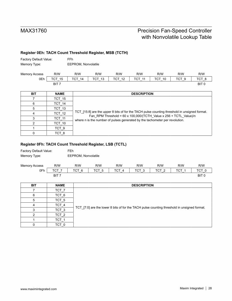
Register 0Fh: TACH Count Threshold Register, LSB (TCTL)
Register 0Eh: TACH Count Threshold Register, MSB (TCTH)
Factory Default Value: FEhMemory Type: EEPROM, Nonvolatile
Memory Access R/W R/W R/W R/W R/W R/W R/W R/W0Fh TCT_7 TCT_6 TCT_5 TCT_4 TCT_3 TCT_2 TCT_1 TCT_0
BIT 7 BIT 0
BIT NAME DESCRIPTION7 TCT_7
TCT_[7:0] are the lower 8 bits of for the TACH pulse counting threshold in unsigned format.
6 TCT_65 TCT_54 TCT_43 TCT_32 TCT_21 TCT_10 TCT_0
Factory Default Value: FFhMemory Type: EEPROM, Nonvolatile
Memory Access R/W R/W R/W R/W R/W R/W R/W R/W0Eh TCT_15 TCT_14 TCT_13 TCT_12 TCT_11 TCT_10 TCT_9 TCT_8
BIT 7 BIT 0
BIT NAME DESCRIPTION7 TCT_15
TCT_[15:8] are the upper 8 bits of for the TACH pulse counting threshold in unsigned format.Fan_RPM Threshold = 60 x 100,000/(TCTH_Value x 256 + TCTL_Value)/n
where n is the number of pulses generated by the tachometer per revolution.
6 TCT_145 TCT_134 TCT_123 TCT_112 TCT_101 TCT_90 TCT_8
MAX31760 Precision Fan-Speed Controller with Nonvolatile Lookup Table
www.maximintegrated.com Maxim Integrated │ 28

Registers 10h–17h: General-Purpose User EEPROM (USER)
Registers 20h–4Fh: 48-Byte Lookup Table (LUT)
Register 50h: Direct Duty-Cycle Control Register (PWMR)
Factory Default Value: 00hMemory Type: EEPROM, Nonvolatile
Memory Access R/W R/W R/W R/W R/W R/W R/W R/W10h–17h
BIT 7 BIT 0
Factory Default Value: FFhMemory Type: EEPROM, Nonvolatile
Memory Access R/W R/W R/W R/W R/W R/W R/W R/W20h–4Fh See Table 7
BIT 7 BIT 0
Default Value: FFhMemory Type: SRAM, Volatile
Memory Access R/W R/W R/W R/W R/W R/W R/W R/W50h PWMR7 PWMR6 PWMR5 PWMR4 PWMR3 PWMR2 PWMR1 PWMR 0
BIT 7 BIT 0
BIT NAME DESCRIPTION7 PWMR7
PWMR[7:0] determine the PWM duty cycle per Table 9 in direct control mode (DFC bit (CR2.0) = 1)
6 PWMR65 PWMR54 PWMR43 PWMR32 PWMR21 PWMR10 PWMR0
MAX31760 Precision Fan-Speed Controller with Nonvolatile Lookup Table
www.maximintegrated.com Maxim Integrated │ 29

Register 51h: Current PWM Duty-Cycle Register (PWMV)
Register 52h: TACH1 Count Register, MSB (TC1H)
Default Value: 00hMemory Type: SRAM, Volatile
Memory Access R R R R R R R R51h PWMV7 PWMV6 PWMV5 PWMV4 PWMV3 PWMV2 PWMV1 PWMV 0
BIT 7 BIT 0
BIT NAME DESCRIPTION7 PWMV7
PWMV[7:0] store the current PWM duty cycle at all times, including during fan failure.
6 PWMV65 PWMV54 PWMV43 PWMV32 PWMV21 PWMV10 PWMV0
Default Value: 00hMemory Type: SRAM, Volatile
Memory Access R R R R R R R R52h TC1_15 TC1_14 TC1_13 TC1_12 TC1_11 TC1_10 TC1_9 TC1_8
BIT 7 BIT 0
BIT NAME DESCRIPTION7 TC1_15
TC1_[15:8] are the higher 8 bits for the TACH1 pulse counting in unsigned format.Fan_RPM = 60 x 100,000/(TC1H_Value x 256 + TC1L_Value)/n
where n is the number of pulses generated by the tachometer per revolution.
6 TC1_145 TC1_134 TC1_123 TC1_112 TC1_101 TC1_90 TC1_8
MAX31760 Precision Fan-Speed Controller with Nonvolatile Lookup Table
www.maximintegrated.com Maxim Integrated │ 30
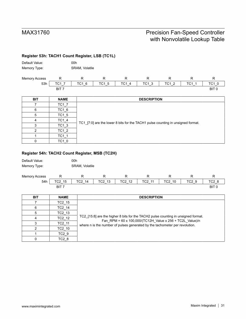
Register 53h: TACH1 Count Register, LSB (TC1L)
Register 54h: TACH2 Count Register, MSB (TC2H)
Default Value: 00hMemory Type: SRAM, Volatile
Memory Access R R R R R R R R53h TC1_7 TC1_6 TC1_5 TC1_4 TC1_3 TC1_2 TC1_1 TC1_0
BIT 7 BIT 0
BIT NAME DESCRIPTION7 TC1_7
TC1_[7:0] are the lower 8 bits for the TACH1 pulse counting in unsigned format.
6 TC1_65 TC1_54 TC1_43 TC1_32 TC1_21 TC1_10 TC1_0
Default Value: 00hMemory Type: SRAM, Volatile
Memory Access R R R R R R R R54h TC2_15 TC2_14 TC2_13 TC2_12 TC2_11 TC2_10 TC2_9 TC2_8
BIT 7 BIT 0
BIT NAME DESCRIPTION7 TC2_15
TC2_[15:8] are the higher 8 bits for the TACH2 pulse counting in unsigned format.Fan_RPM = 60 x 100,000/(TC12H_Value x 256 + TC2L_Value)/n
where n is the number of pulses generated by the tachometer per revolution.
6 TC2_145 TC2_134 TC2_123 TC2_112 TC2_101 TC2_90 TC2_8
MAX31760 Precision Fan-Speed Controller with Nonvolatile Lookup Table
www.maximintegrated.com Maxim Integrated │ 31
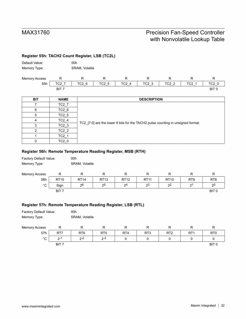
Register 57h: Remote Temperature Reading Register, LSB (RTL)
Register 56h: Remote Temperature Reading Register, MSB (RTH)
Register 55h: TACH2 Count Register, LSB (TC2L)
Factory Default Value: 00hMemory Type: SRAM, Volatile
Memory Access R R R R R R R R57h RT7 RT6 RT5 RT4 RT3 RT2 RT1 RT0
°C 2-1 2-2 2-3 0 0 0 0 0BIT 7 BIT 0
Factory Default Value: 00hMemory Type: SRAM, Volatile
Memory Access R R R R R R R R56h RT15 RT14 RT13 RT12 RT11 RT10 RT9 RT8
°C Sign 26 25 24 23 22 21 20
BIT 7 BIT 0
Default Value: 00hMemory Type: SRAM, Volatile
Memory Access R R R R R R R R55h TC2_7 TC2_6 TC2_5 TC2_4 TC2_3 TC2_2 TC2_1 TC2_0
BIT 7 BIT 0
BIT NAME DESCRIPTION7 TC2_7
TC2_[7:0] are the lower 8 bits for the TACH2 pulse counting in unsigned format.
6 TC2_65 TC2_54 TC2_43 TC2_32 TC2_21 TC2_10 TC2_0
MAX31760 Precision Fan-Speed Controller with Nonvolatile Lookup Table
www.maximintegrated.com Maxim Integrated │ 32

Register 59h: Local Temperature Reading Register, LSB (LTL)
Register 58h: Local Temperature Reading Register, MSB (LTH)
Factory Default Value: 00hMemory Type: SRAM, Volatile
Memory Access R R R R R R R R59h LT7 LT6 LT5 LT4 LT3 LT2 LT1 LT0
°C 2-1 2-2 2-3 0 0 0 0 0BIT 7 BIT 0
Factory Default Value: 00hMemory Type: SRAM, Volatile
Memory Access R R R R R R R R58h LT15 LT14 LT13 LT12 LT11 LT10 LT9 LT8
°C Sign 26 25 24 23 22 21 20
BIT 7 BIT 0
Register 5Ah: Status Register (SR)
Default Value: 00hMemory Type: SRAM, Volatile
Memory Access R R R R R R R R5Ah PC bit RDFA LHA LOTA RHA ROTA TACH2A TACH1A
BIT 7 BIT 0Note: Alarm bits in the SR register are cleared upon reading. If a fault is detected again after clearing, it is set again.
BIT NAME DESCRIPTION
7 PC bit
Program Corrupt Bit0 = No EEPROM data corruption detected.1= An error has occurred during EEPROM programming. A successful write to EEPROM must occur followed by a POR or soft-POR before this bit will reset to 0.
6 RDFA
Remote Diode Fault Alarm0 = Remote diode functions properly (default).1 = Remote diode open-circuit or short-circuit fault detected. This fault does not trigger the ALERT output.
5 LHALocal High Temperature Alarm0 = The temperature of the IC die is at or lower than the local high set point (default).1 = The temperature of the IC die is higher than the local high set point.
4 LOTALocal Overtemperature Alarm0 = The local temperature is at or lower than the local overtemperature set point (default).1 = The local temperature is higher than the local overtemperature set point.
MAX31760 Precision Fan-Speed Controller with Nonvolatile Lookup Table
www.maximintegrated.com Maxim Integrated │ 33

Register 5Bh: EEPROM LOAD/WRITE Register (EEX)
Register 5Ah: Status Register (SR) (continued)
Factory Default Value: 00hMemory Type: SRAM, Volatile
Memory Access R/W N/A N/A R/W R/W R/W R/W R/W5Bh L/W Reserved Reserved 40h–4Fh 30h–3Fh 20h–2Fh 10h–1Fh 00h–0Fh
BIT 7 Clears to 00h when read. BIT 0
BIT NAME DESCRIPTION
7 L/W 0 = Write RAM to EEPROM1 = Load EEPROM to RAM
6 Reserved Reserved
5 Reserved Reserved
4 40h–4Fh 1 = Bytes 40h through 4Fh
3 30h–3Fh 1 = Bytes 30h through 3Fh
2 20h–2Fh 1 = Bytes 20h through 2Fh
1 10h–1Fh 1 = Bytes 10h through 1Fh
0 00h–0Fh 1 = Bytes 00h through 0Fh
BIT NAME DESCRIPTION
3 RHARemote Temperature High Alarm0 = The temperature of the remote diode is at or lower than the remote high set point (default).1 = The temperature of the remote diode is higher than the remote high set point.
2 ROTA
Remote Overtemperature Alarm0 = The temperature of the remote diode is at or lower than the overtemperature set point (default).1 = The temperature of the remote diode is higher than the overtemperature set point.
1 TACH2A
TACH2 Alarm0 = The fan sensed by TACH2 is running properly (default).If tachometer pulses are provided to TACH2, this means the TACH2 count is lower than or equal to the value in TACH Count Threshold registers (the fan is running at an RPM higher than the minimum acceptable value).If RD signal is provided to TACH2, this means the fan is running.1 = The fan sensed by TACH2 is not running properly. This happens when the fan is running at an RPM lower than the minimum acceptable value, or the fan is not rotating at all, or an overflow occurred during counting.
0 TACH1A
TACH1 Alarm0 = The fan sensed by TACH1 is running properly.If tachometer pulses are provided to TACH1, this means the TACH1 count is lower than or equal to the value in TACH Count Threshold registers (the fan is running at an RPM higher than the minimum acceptable value).If RD signal is provided to TACH1, this means the fan is running.1 = The fan sensed by TACH1 is not running properly. This happens when the fan is running at an RPM lower than the minimum acceptable value, or the fan is not rotating at all, or an overflow occurred during counting.
MAX31760 Precision Fan-Speed Controller with Nonvolatile Lookup Table
www.maximintegrated.com Maxim Integrated │ 34

Applications InformationADC Noise FilteringThe integrating ADC has inherently good noise rejection, especially of low-frequency signals such as 60Hz/120Hz power-supply hum. However, micropower operation plac-es constraints on high-frequency noise rejection. Lay out the PCB carefully with proper external noise filtering for high-accuracy remote measurements in electrically noisy environments. Filter high-frequency electromag-netic interference (EMI) at the DXP pin with an external 2200pF capacitor connected between DXP and DXN. A capacitance higher than 2200pF introduces errors due to the rise time of the switched-current source.
Power-Supply Decoupling To achieve the best results when using the device, decou-ple the VDD power supply with a 0.1μF capacitor. Use a high-quality, ceramic, surface-mount capacitor if possible. Surface-mount components minimize lead inductance, which improves performance, and ceramic capacitors tend to have adequate high-frequency response for decoupling applications.
Twisted Pairs and Shielded CablesFor remote-sensor distances longer than 8in, or in partic-ularly noisy environments, a twisted pair is recommended. Its practical length is 6ft to 12ft (typ) before noise becomes a problem, as tested in a noisy electronics laboratory. For longer distances, the best solution is a shielded twisted pair like that used for audio microphones. For example, Belden 8451 works well for distances up to 100ft in a noisy environment. Connect the twisted pair to DXP and DXN and the shield to ground, and leave the shield’s remote end unterminated. Excess capacitance at DXP limits practical remote-sensor distances. For very long cable runs, the cable’s parasitic capacitance often provides noise filtering, so the recommended 2200pF capacitor can often be removed or reduced in value. Cable resistance also affects remote-sensor accuracy. A 1Ω series resistance introduces about +1/2°C error.
PCB Layout Checklist1) When possible, place the device as close as possible
to the remote diode. In a noisy environment, such as a computer motherboard, this distance can be 4in to 8in or more, as long as the worst noise sources (such as CRTs, clock generators, memory buses, and ISA/PCI buses) are avoided.
2) Do not route the DXP lines next to the deflection coils of a CRT. Also, do not route the traces across a fast memory bus, which can easily introduce +30°C error, even with good filtering. Otherwise, most noise sources are fairly benign.
3) Route the DXP and DXN traces parallel and close to each other, away from any high-voltage traces such as +12V DC. Avoid leakage currents from PCB contamination.
4) Route as few vias and crossunders as possible to minimize copper/solder thermocouple effects.
5) When connecting a thermocouple, make sure that both the DXP and the DXN paths have matching thermocouples leads. In general, PCB-induced ther-mocouples are not a serious problem. A copper solder thermocouple exhibits 3µV/°C, and it takes approxi-mately 200µV of voltage error at DXP/GND to cause a +1°C measurement error, so most parasitic thermo-couple errors are swamped out.
6) Use wide traces. Narrow traces are more inductive and tend to pick up radiated noise. The 10-mil widths and spacings are recommended, but are not absolutely necessary (as they offer only a minor improvement in leakage and noise), but use them where practical.
7) Placing an electrically clean copper ground plane between the DXP and DXN traces and traces carrying high-frequency noise signals helps reduce EMI.
MAX31760 Precision Fan-Speed Controller with Nonvolatile Lookup Table
www.maximintegrated.com Maxim Integrated │ 35

+Denotes a lead(Pb)-free/RoHs-compliant package.
PART TEMP RANGE PIN-PACKAGE
MAX31760AEE+ -40NC to +125NC 16 QSOP
MAX31760AEE+T -40NC to +125NC 16 QSOP
Ordering Information
PACKAGE TYPE
PACKAGE CODE
OUTLINE NO.
LAND PAT-TERN NO.
16 QSOP E16+1 21-0055 90-0167
Package InformationFor the latest package outline information and land patterns (foot-prints), go to www.maximintegrated.com/packages. Note that a “+”, “#”, or “-” in the package code indicates RoHS status only. Package drawings may show a different suffix character, but the drawing pertains to the package regardless of RoHS status.
MAX31760 Precision Fan-Speed Controller with Nonvolatile Lookup Table
www.maximintegrated.com Maxim Integrated │ 36

Revision HistoryREVISIONNUMBER
REVISIONDATE DESCRIPTION PAGES
CHANGED0 4/14 Initial release —
For pricing, delivery, and ordering information, please contact Maxim Direct at 1-888-629-4642, or visit Maxim Integrated’s website at www.maximintegrated.com.
Maxim Integrated cannot assume responsibility for use of any circuitry other than circuitry entirely embodied in a Maxim Integrated product. No circuit patent licenses are implied. Maxim Integrated reserves the right to change the circuitry and specifications without notice at any time. The parametric values (min and max limits) shown in the Electrical Characteristics table are guaranteed. Other parametric values quoted in this data sheet are provided for guidance.
Maxim Integrated and the Maxim Integrated logo are trademarks of Maxim Integrated Products, Inc. © 2014 Maxim Integrated Products, Inc. │ 37
MAX31760 Precision Fan-Speed Controller with Nonvolatile Lookup Table