max6955 evaluation kit - maxim integrated · the max6955 ev kit software has 43 register tabs for...
TRANSCRIPT
General DescriptionThe MAX6955 evaluation kit (EV kit) is designed to eval-uate the MAX6955 light-emitting diode (LED) display dri-ver with a 2-wire interface. The EV kit board contains twoMAX6955 LED display drivers on symmetrical sides ofthe board, allowing a 16-digit display using sixteen 14-segment alphanumeric LEDs. The DB-25 connectorallows a PC’s parallel (printer) port to provide the 2-wireinterface. The Windows® software provides a friendlygraphical user interface (GUI) to exercise the features ofthe MAX6955 by allowing on-the-fly text and numericentry and access to all relevant registers. The softwareincludes multiple tabs for accessing the various regis-ters and maintains a consistent format with controls onthe left side of the software’s main window pertaining toU1, located on the left side of the EV kit board. Similarly,all the controls on the right side of the software’s mainwindow pertain to U2, located on the right side of the EVkit board. The EV kit board requires a 3.3VDC or 5VDCpower supply and jumpers JU1–JU4 allow the user tomanually modify the device address of U1 or U2.
Order the MAX6955EVKIT for comprehensive evalua-tion of the MAX6955 using a PC with an available paral-lel port.
Features Proven PC Board Layout
Windows 95/98/ME/NT/2000/XP-CompatibleEvaluation Software
2-Wire Serial Interface
Sixteen 14-Segment Bright LEDs
Fully Assembled and Tested
Eva
lua
tes: M
AX
69
55
MAX6955 Evaluation Kit
________________________________________________________________ Maxim Integrated Products 1
19-2708; Rev 0; 12/02
Component List
For pricing, delivery, and ordering information, please contact Maxim/Dallas Direct! at 1-888-629-4642, or visit Maxim’s website at www.maxim-ic.com.
DESIGNATION QTY DESCRIPTION
C1 122µF ±20%, 6.3V X5R ceramiccapacitor (1210)TDK C3225X5R0J226M
C2 112pF ±5%, 50V COG ceramiccapacitor (0603)TDK C1608COG1H120JT
C3, C5 20.1µF ±10%, 25V X7R ceramiccapacitors (0603)TDK C1608X7R1E104KT
C4, C6 21µF ±20%, 10V X5R ceramiccapacitors (0805)TDK C2012X5R1A105M
D1–D8 8
0.54in dual 14-segmentalphanumeric LEDsLumex LDD-F5406RIFairchild MDA6140C
D9–D12 4Zener diodes, Vz = 5.1V (3-pinSOT23), top mark: KZ2 or Z2Diodes Inc. BZX84C5V1
Ordering Information
PART TEMP RANGE IC PACKAGE
MAX6955EVKIT 0°C to +70°C 36 SSOP
MAX6955 EV Kit Files PROGRAM DESCRIPTION
INSTALL.EXE Installs the EV kit software
MAX6955.EXE Application program
HELPFILE.HTM MAX6955 EV kit Helpfile
PORT95NT.EXE SST's freeware DLPortIO driver package
UNINST.INI Uninstalls the EV kit software
Windows is a registered trademark of Microsoft Corp.
DESIGNATION QTY DESCRIPTION
J1 1 Male DB-25 right-angle plug
J2, J3 2 20-pin dual-row 2 x 10 headers
JU1–JU4 4 5-pin headers
N1, N2 2N-channel MOSFETs (3-pin SOT23),top mark: 702Central Semiconductor 2N7002
Q1, Q2 2Bipolar junction transistors (3-pinSOT23), top mark: C1ACentral Semiconductor CMPT3904
R1, R5 2 100kΩ ±5% resistors (1206)
R2, R6 2 13kΩ ±5% resistors (1206)
R3, R4,R7–R10,R13–R22
16 47kΩ ±5% resistors (1206)
R11, R12 2 100kΩ ±1% resistors (1206)
U1, U2 2 MAX6955AAX (36-pin SSOP)
None 4 Shunts

Eva
lua
tes:
M
AX
69
55
MAX6955 Evaluation Kit
2 _______________________________________________________________________________________
Quick StartRecommended Equipment
Before beginning, the following equipment is needed:
• MAX6955EVKIT
• A 3.3VDC or 5VDC power supply
• PC with Windows 95/98/ME/NT/2000/XP
• An available parallel port (female DB-25 connectoron back of PC)
• A standard 25-pin, straight-through, male-to-femalecable to connect the PC ’s parallel port to theMAX6955 EV kit board
Procedure1) Connect a cable from the PC’s parallel port to the
MAX6955 EV kit board. Use a 25-pin, straight-through, female-to-male cable.
2) Install the supplied CD into the CD drive of your PCand run INSTALL.EXE. When the installer windowshows up on the screen, press the INSTALL button.The MAX6955 program files are copied and iconsare created in the Programs section within the Startmenu. When you see the self-extracting DLPortIOdriver install window appear on the screen, pressthe Yes button. This automatically unpacks the com-pressed files and runs the DLPortIO driver installer.If using Windows NT, 2000, or XP, you must haveadministrator privileges on your PC. If you do not,then contact your system administrator to allowinstallation. You need to restart your PC afterinstalling the DLPortIO driver.
3) Connect a 3.3VDC or 5VDC power supply betweenthe VCC and GND pads on the MAX6955 EV kitboard.
4) Start the MAX6955 EV kit program by double click-ing its icon located in the Programs section withinthe Start menu.
5) The program automatically detects the MAX6955 EVkit board and displays 2-wire Hardware Detected ina green font.
6) The MAX6955 EV kit board and MAX6955 EV kit soft-ware should automatically display MAX6955 EVKIT.
Software DescriptionThe EV kit software’s main window, shown in Figure 1,allows on-the-fly text and numeric entry and also allowsaccess to all the relevant registers for easy configuration.The controls on the left side of the software’s main win-dow control U1 and similarly, the controls on the rightside of the software’s main window control U2. Each reg-ister has its own tab in the order of the MAX6955’saddress map. A 2-wire operation field is present at thevery bottom of the software’s main window, which showsthe results of the last 2-wire operation.
Alphanumeric Entry for U1In the upper left-hand corner of the software’s mainwindow is the Alphanumeric Entry for U1 group box.This group box has five main controls:
• Plane group box
• U1 Address (write) combo box
• U1 Address (read) combo box
• Alphanumeric entry field
• Decimal Point checkbox and individual decimalpoint checkboxes
The first control is the Plane group box, which allowsthe user to select which plane to write to. The radio but-ton choices in the Plane group box are P0 and P1, P0,and P1. It is important to note that once one of theseplane radio buttons is selected, the software automati-cally takes the text or numbers that exist in theAlphanumeric Entry field and writes them to the display.
The second and third controls are the U1 Address(write) and the U1 Address (read) combo boxes.These device-address combo boxes default to 0xCAfor write and 0xCB for read. If you modify the defaultdevice address, change the jumper settings on JU1and JU2 on the MAX6955 EV kit board. If the defaultaddress settings are changed on the board, the usermust also manually select the correct device address
Component Suppliers
SUPPLIER PHONE WEBSITE
CentralSemiconductor
631-435-1110 www.centralsemi.com
Diodes Inc. 805-446-4800 www.diodes.com
FairchildSemiconductor
888-522-5372 www.fairchildsemi.com
Lumex, Inc. 800-278-5666 www.lumex.com
Scientific SoftwareTools, Inc.
610-891-1640 www.sstnet.com
TDK 847-803-6100 w w w .com p onent.td k.com

in the U1 Address (write) and the U1 Address (read)combo boxes. Table 1 lists the device address selec-tion for the various JU1 and JU2 jumper settings.
The fourth control is the Alphanumeric Entry field,which displays MAX6955 at the start of the program.The user may type letters, numbers, apostrophes, com-mas, or even spaces in the Alphanumeric Entry fieldusing the computer’s keyboard. The AlphanumericEntry field also supports standard word processing fea-tures like highlighting, insert, and delete. Anytime aninvalid character is typed into the Alphanumeric Entryfield, such as an @, a character error message boxpops up, indicating an invalid character was typed.
Anytime a valid character is typed into the Alpha-numeric Entry field, the software automatically writes itto the corresponding digit on the display.
The last control type within the Alphanumeric Entryfor U1 group box is the Decimal Point checkbox andthe individual decimal point checkboxes. When theDecimal Point checkbox is checked, all of the individ-ual decimal point checkboxes become visible. Whenthe Decimal Point checkbox is unchecked, all of theindividual decimal point checkboxes are hidden.Checking one of the individual decimal point check-boxes automatically lights up the corresponding deci-mal point on the board.
Eva
lua
tes: M
AX
69
55
MAX6955 Evaluation Kit
_______________________________________________________________________________________ 3
Figure 1. MAX6955 EV Kit Software’s Main Window

Eva
lua
tes:
M
AX
69
55 Alphanumeric Entry for U2
The Alphanumeric Entry for U2 group box is in theupper right-hand corner of the software’s main window.This group box has five main controls:
• Plane group box
• U2 Address (write) combo box
• U2 Address (read) combo box
• Alphanumeric Entry Field
• Decimal Point checkbox and individual decimalpoint checkboxes
The first control is the Plane group box, which allowsthe user to select which plane to write to. The radio but-ton choices in the Plane group box are P0 and P1, P0,and P1. It is important to note that once one of theseplane radio buttons is selected, the software automati-cally takes the text or numbers that exist in theAlphanumeric Entry field and writes them to the display.
The second and third controls are the U2 Address(write) and the U2 Address (read) combo boxes.These device address combo boxes default to 0xC0 forwrite and 0xC1 for read. If you modify the defaultdevice address, change the jumper settings on JU3and JU4 on the MAX6955 EV kit board. If the defaultaddress settings are changed on the board, the usermust also manually select the correct device address inthe U2 Address (write) and the U2 Address (read)combo boxes. Table 2 lists the device address selec-tion for the various JU3 and JU4 jumper settings.
The fourth control is the Alphanumeric Entry field, whichdisplays EVKIT at the start of the program. The usermay type letters, numbers, apostrophes, commas, oreven spaces in the Alphanumeric Entry field using thecomputer’s keyboard. The Alphanumeric Entry fieldalso supports standard word processing features likehighlighting, insert, and delete. Anytime an invalid char-acter is typed into the Alphanumeric Entry field, suchas an @, a character error message box pops up, indi-cating an invalid character was typed. Anytime a validcharacter is typed into the Alphanumeric Entry field, thesoftware automatically writes it to the correspondingdigit on the display.
The last control type within the Alphanumeric Entryfor U2 group box is the Decimal Point checkbox andthe individual decimal point checkboxes. When theDecimal Point checkbox is checked, all of the individ-ual decimal point checkboxes become visible. Whenthe Decimal Point checkbox is unchecked, all of theindividual decimal point checkboxes are hidden.
Checking one of the individual decimal point checkbox-es automatically lights up the corresponding decimalpoint on the board.
Register TabsThe MAX6955 EV kit software has 43 register tabs forboth U1 and U2, giving access to 86 unique registers.Any register tab can be selected by a mouse clickwhen visible and not all register tabs can be visible atonce. Scroll through the register tabs using the left andright scroll arrows located on the right-hand side of thesoftware’s main window. The order of the register tabscorresponds to the same order of the MAX6955’saddress map. Refer to the MAX6955 IC data sheet fordetails on the address map and a complete descriptionof each register.
Keyboard NavigationWhen you type on the keyboard, the system must knowwhich control should receive the keys. Press the tabkey to move the keyboard’s focus from one control tothe next. The focused control is indicated by a dottedoutline. Shift + tab moves the focus to the previouslyfocused control. Buttons respond to the keyboard’sspace bar. Some controls respond to the keyboard’sup and down arrow keys. Activate the program’s menubar by pressing the F10 key, then press the letter of themenu item you want. Most menu items have one letterunderlined, indicating their shortcut key.
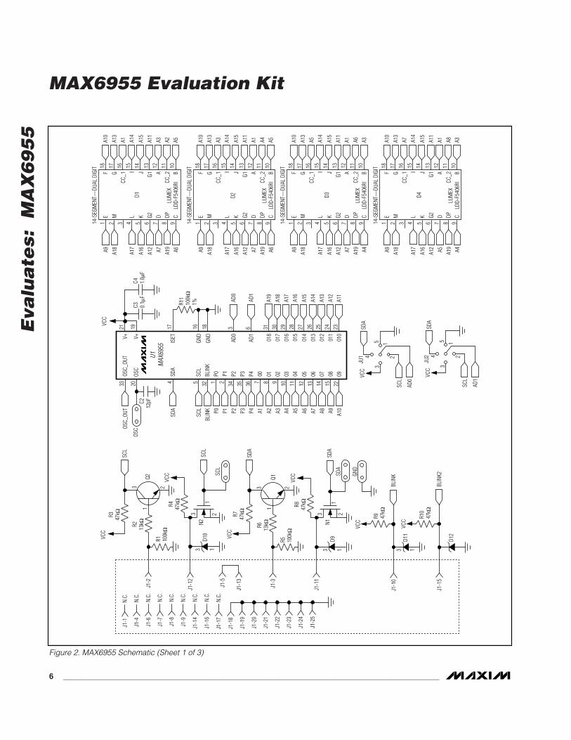
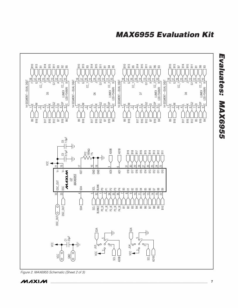
Hardware DescriptionThe MAX6955 EV kit board is designed symmetricallyso that the left side of the board pertains to U1 and theright side of the board pertains to U2. Thus, the firsteight digits are driven by U1 and the last eight digitsare driven by U2. An OSC pad for U1 is provided forexternal clock operation and an OSC_OUT pad for U2is also provided for cascading additional MAX6955devices. The DB-25 connector and associated circuitryare only needed for obtaining the 2-wire interface fromthe PC’s parallel port and are not needed in typicalapplications. Connect the DB-25 connector, J1, to thePC’s parallel port using a 25-pin straight-through,female-to-male cable. Four jumpers are on the EV kitboard to modify the device address for U1 and U2. Thetwo dual-row 20-pin headers, J2 and J3, are used forthe I/O expander and keyscan features of U1 and U2,respectively.
Device Address Jumpers JU1–JU4The MAX6955 EV kit board contains four jumpers in thetop right-hand corner of the board. Jumpers JU1 and
MAX6955 Evaluation Kit
4 _______________________________________________________________________________________

JU2 select the device address for U1 and jumpers JU3and JU4 select the device address for U2. Table 1 liststhe device address selection for the various JU1 andJU2 jumper settings. Table 2 lists the device addressselection for the various JU3 and JU4 jumper settings.Before changing the default device address for U1 orU2, read the Alphanumeric Entry for U1 andAlphanumeric Entry for U2 sections pertaining torequired modifications for the Address (write) andAddress (read) combo boxes.
OSC and OSC_OUT PadsAn OSC pad for U1 is provided for external clock oper-ation and an OSC_OUT pad for U2 is also provided forcascading additional MAX6955 devices. When theOSC pad is unconnected, the internal oscillator of U1
drives both U1 and U2 because OSC_OUT of U1 isdirectly connected to OSC of U2 with a trace on theboard. It is also possible to drive the OSC pad of U1with an external clock between 1MHz to 8MHz.
SCL, SDA, and GND PadsThe MAX6955 EV kit utilizes the PC’s parallel port togenerate a 2-wire interface for easy evaluation.Customers who wish to evaluate U1 and U2 using theirown 2-wire interface must remove the parallel portcable from the board and attach the new 2-wire inter-face to the SCL, SDA, and GND pads located on theupper left-hand side of the MAX6955 EV kit board. TheSCL, SDA, and GND pads are also useful for probingthe 2-wire waveforms with a digital oscilloscope or logicanalyzer.
Eva
lua
tes: M
AX
69
55
MAX6955 Evaluation Kit
_______________________________________________________________________________________ 5
Table 1. U1 Address Selection forJumpers JU1 and JU2
JUMPER POSITION DEVICE ADDRESS
JU1 JU2 (Write) (Read)
1-2 1-2 0xDE 0xDF
1-3 1-2 0xDA 0xDB
1-4 1-2 0xDC 0xDD
1-5 1-2 0xD8 0xD9
1-2 1-3 0xCE 0xCF
1-3* 1-3* 0xCA* 0xCB*
1-4 1-3 0xCC 0xCD
1-5 1-3 0xC8 0xC9
1-2 1-4 0xD6 0xD7
1-3 1-4 0xD2 0xD3
1-4 1-4 0xD4 0xD5
1-5 1-4 0xD0 0xD1
1-2 1-5 0xC6 0xC7
1-3 1-5 0xC2 0xC3
1-4 1-5 0xC4 0xC5
1-5 1-5 0xC0 0xC1
*Default for U1.
Table 2. U2 Address Selection forJumpers JU3 and JU4
JUMPER POSITION DEVICE ADDRESS
JU3 JU4 (Write) (Read)
1-2 1-2 0xDE 0xDF
1-3 1-2 0xDA 0xDB
1-4 1-2 0xDC 0xDD
1-5 1-2 0xD8 0xD9
1-2 1-3 0xCE 0xCF
1-3 1-3 0xCA 0xCB
1-4 1-3 0xCC 0xCD
1-5 1-3 0xC8 0xC9
1-2 1-4 0xD6 0xD7
1-3 1-4 0xD2 0xD3
1-4 1-4 0xD4 0xD5
1-5 1-4 0xD0 0xD1
1-2 1-5 0xC6 0xC7
1-3 1-5 0xC2 0xC3
1-4 1-5 0xC4 0xC5
1-5* 1-5* 0xC0* 0xC1*
*Default for U2.
Eva
lua
tes:
M
AX
69
55
MAX6955 Evaluation Kit
6 _______________________________________________________________________________________
J1-1
N.C.
J1-4
N.C.
J1-6
N.C.
J1-1
2
J1-2
VCC
VCC
VCC
Q2 Q1
VCC
VCC
VCC
VCC
3
JU1 4
5
21
3
1
1
1
N1
3 2
3 21
3N2
2
2
SCL
SCL
SCL
SDA
OSC_
OUT
V+ V+
ISET
GND
GND
OSC
3321
VCC
19 17 16 18 3 6
20C2
12pF
C4 1.0µ
F
R11
100k
Ω1%C3 0.1µ
F
4
AD0
SDA
SDA
BLIN
K
BLIN
K2SDA
GND
SCL
R3 47kΩ
R4 47kΩ R8 47kΩ
R7 47kΩ
R6 13kΩ
R5 100k
Ω
R2 13kΩ
J1-7
N.C.
J1-8
N.C.
J1-9
N.C.
J1-1
4N.
C.
J1-1
6N.
C.
J1-1
7
J1-1
8
J1-1
9
J1-2
0
J1-2
1
J1-2
2
J1-2
3
J1-2
4
J1-2
5
N.C.
J1-5
J1-1
3
SDA
5SC
L32
BLIN
K1
P02
P134
P235
P336
P47
008
019
0210
0311
0412
0513
0614
0715
0822
31 30 29 28 27 26 25 24 2309
OSC_
OUT
OSC
SDA
SCL
BLIN
K P0 P1 P2 P3 P4 A1 A2 A3 A4 A5 A6 A7 A8 A9 A10
018
017
016
015
014
013
012
011
010
J1-3
J1-1
1
J1-1
5
J1-1
0
R1 100k
Ω
D10
3 1
D9
R10
47kΩ
R9 47kΩ
3 1
D11
3 1
D12
VCC
JU2 4
5
21
3
SCL
SDA
AD1
U1M
AX69
55
AD0
AD1
A19
A18
A17
A16
A15
A14
A13
A12
A11
AD0
AD1
1E
2M
3 4L
5K
6G2
7D
8DP
9
1814
-SEG
MEN
T—DU
AL D
IGIT
LUM
EXLD
D-F5
406R
I
D1 D2 D3 D4
17 16 15 14 13 12 11 10C
A9 A18
A17
A16
A12 A7 A19 A6
F GCC
_1I J G1 A
CC_2 B
A10
A13
A1 A14
A15
A11
A3 A2 A5
1E
2M
3 4L
5K
6G2
7D
8DP
9
1814
-SEG
MEN
T—DU
AL D
IGIT
LUM
EXLD
D-F5
406R
I
17 16 15 14 13 12 11 10C
A9 A18
A17
A16
A12 A7 A19 A6
F GCC
_1I J G1 A
CC_2 B
A10
A13
A3 A14
A15
A11
A1 A4 A5
1E
2M
3 4L
5K
6G2
7D
8DP
9
1814
-SEG
MEN
T—DU
AL D
IGIT
LUM
EXLD
D-F5
406R
I
17 16 15 14 13 12 11 10C
A9 A18
A17
A16
A12 A7 A19 A4
F GCC
_1I J G1 A
CC_2 B
A10
A13
A5 A14
A15
A11
A1 A6 A3
1E
2M
3 4L
5K
6G2
7D
8DP
9
1814
-SEG
MEN
T—DU
AL D
IGIT
LUM
EXLD
D-F5
406R
I
17 16 15 14 13 12 11 10C
A9 A18
A17
A16
A12 A5 A19 A4
F GCC
_1I J G1 A
CC_2 B
A10
A13
A7 A14
A15
A11
A1 A8 A3
Figure 2. MAX6955 Schematic (Sheet 1 of 3)
Eva
lua
tes: M
AX
69
55
MAX6955 Evaluation Kit
_______________________________________________________________________________________ 7
VCC
JU3 4
5
21
3
SCL
SDA
OSC_
OUT
V+ V+
ISET
GND
GND
OSC
3321
VCC
19 17 16 18 3 6
20C6 1.
0µF
R12
100k
Ω1%C5 0.
1µF
C1 22µF
4
AD0BVC
C
SDA
5SC
L32
BLIN
K1
P02
P134
P235
P336
P47
008
019
0210
0311
0412
0513
0614
0715
0822
31 30 29 28 27 26 25 24 2309
OSC_
OUT
OSC_
OUT
SDA
SCL
BLIN
K2P0
_BP1
_B
P2_B
P3_B
P4_B B1 B2 B3 B4 B5 B6 B7 B8 B9 B1
0
018
017
016
015
014
013
012
011
010
VCC
JU4 4
5
21
3
SCL
SDA
AD1B
U2M
AX69
55
AD0
AD1
B19
B18
B17
B16
B15
B14
B13
B12
B11
AD0B
AD1B
1E
2M
3 4L
5K
6G2
7D
8DP
9
1814
-SEG
MEN
T—DU
AL D
IGIT
LUM
EXLD
D-F5
406R
I
D5 D6 D7 D8
17 16 15 14 13 12 11 10C
B9 B18
B17
B16
B12 B7 B19 B6
F GCC
_1I J G1 A
CC_2 B
B10
B13
B1 B14
B15
B11
B3 B2 B5
1E
2M
3 4L
5K
6G2
7D
8DP
9
1814
-SEG
MEN
T—DU
AL D
IGIT
LUM
EXLD
D-F5
406R
I
17 16 15 14 13 12 11 10C
B9 B18
B17
B16
B12 B7 B19 B6
F GCC
_1I J G1 A
CC_2 B
B10
B13
B3 B14
B15
B11
B1 B4 B5
1E
2M
3 4L
5K
6G2
7D
8DP
9
1814
-SEG
MEN
T—DU
AL D
IGIT
LUM
EXLD
D-F5
406R
I
17 16 15 14 13 12 11 10C
B9 B18
B17
B16
B12 B7 B19 B4
F GCC
_1I J G1 A
CC_2 B
B10
B13
B5 B14
B15
B11
B1 B6 B3
1E
2M
3 4L
5K
6G2
7D
8DP
9
1814
-SEG
MEN
T—DU
AL D
IGIT
LUM
EXLD
D-F5
406R
I
17 16 15 14 13 12 11 10C
B9 B18
B17
B16
B12 B5 B19 B4
F GCC
_1I J G1 A
CC_2 B
B10
B13
B7 B14
B15
B11
B1 B8 B3
GND
VCC
Figure 2. MAX6955 Schematic (Sheet 2 of 3)

Eva
lua
tes:
M
AX
69
55
MAX6955 Evaluation Kit
8 _______________________________________________________________________________________
J2-1
N.C.
J2-2
N.C.
J2-3
N.C.
J2-4
N.C.
J3-1
7N.
C.
J3-1
8N.
C.
J3-1
9N.
C.
J3-2
0N.
C.
J2-5
J2-6
J2-7
J2-8
J2-9
J2-1
0
J2-1
1
J2-1
2
J2-1
3
J2-1
4
J2-1
5
J2-1
6
J2-1
7
J2-1
8
J2-1
9
J2-2
0
P0 P1 P2 P3 P4 A1 A2 A3 A4 A5 A6 A7 A8
VCC
J3-1
J3-2
J3-3
J3-4
J3-5
J3-6
J3-7
J3-8
J3-9
J3-1
0
J3-1
1
J3-1
2
J3-1
3
J3-1
4
J3-1
5
J3-1
6
B7 B6 B5 B4 B3 B2 B1 P4_B
P3_B
P2_B
P1_B
P0_B
R13
47kΩ
VCC
B8P0 P1 P2 P3 P4
P0_B
P1_B
P2_B
P3_B
P4_B
R14
47kΩ R15
47kΩ R16
47kΩ R17
47kΩ R18
47kΩ R19
47kΩ R20
47kΩ R21
47kΩ R22
47kΩ
VCC
Figure 2. MAX6955 Schematic (Sheet 3 of 3)

Eva
lua
tes: M
AX
69
55
MAX6955 Evaluation Kit
_______________________________________________________________________________________ 9
Figure 3. MAX6955 EV Kit Component Placement Guide—Component Side
Eva
lua
tes:
M
AX
69
55
MAX6955 Evaluation Kit
10 ______________________________________________________________________________________
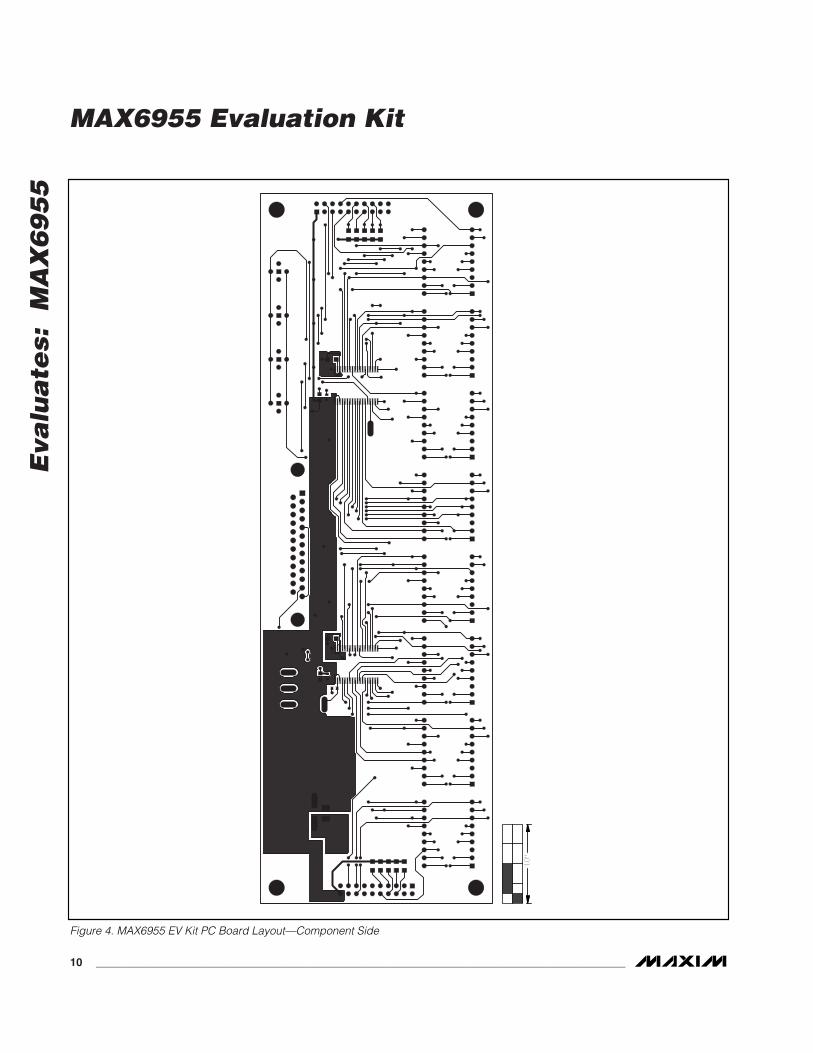
Figure 4. MAX6955 EV Kit PC Board Layout—Component Side
Eva
lua
tes: M
AX
69
55
MAX6955 Evaluation Kit
______________________________________________________________________________________ 11
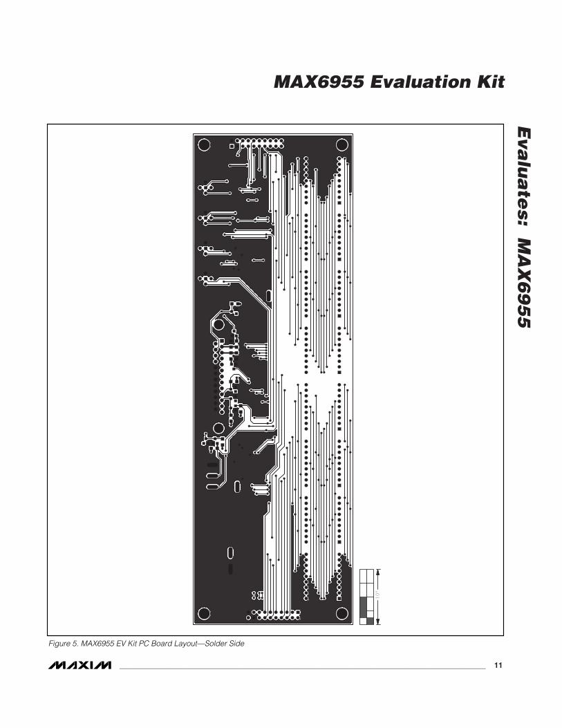
Figure 5. MAX6955 EV Kit PC Board Layout—Solder Side
Maxim cannot assume responsibility for use of any circuitry other than circuitry entirely embodied in a Maxim product. No circuit patent licenses areimplied. Maxim reserves the right to change the circuitry and specifications without notice at any time.
12 ____________________Maxim Integrated Products, 120 San Gabriel Drive, Sunnyvale, CA 94086 408-737-7600
© 2002 Maxim Integrated Products Printed USA is a registered trademark of Maxim Integrated Products.
Eva
lua
tes:
M
AX
69
55
MAX6955 Evaluation Kit
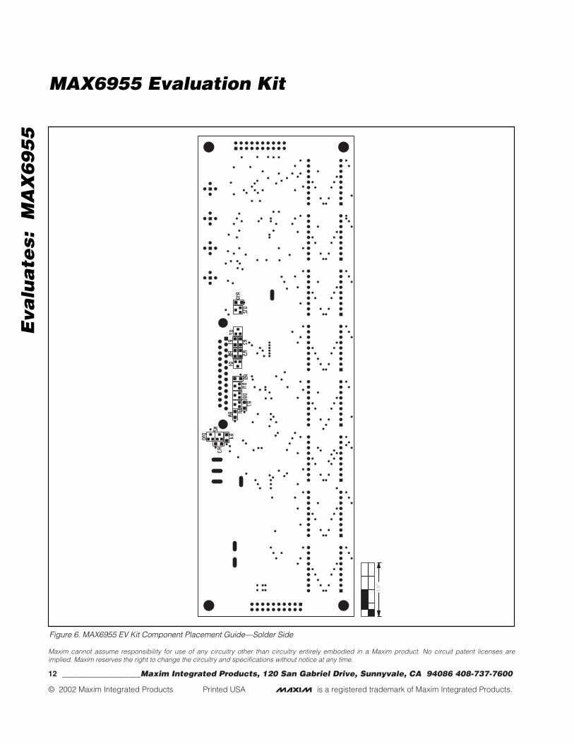
Figure 6. MAX6955 EV Kit Component Placement Guide—Solder Side