may 31, 2000 vhdl class cpu project - web services...
TRANSCRIPT

CPU Project
VHDL ClassMay 31, 2000
Trudy Lary

Project Goals:
1. Write VHDL code for a simple 16-bit CPU
2. Write testbenches for the major CPU blocks
3. Simulate testbenches using ModelTech’s Modelsim
4. Synthesize the VHDL into gates using Synopsys’ Design Compiler Technology Toshiba’s 0.25u Standard cell
5. Insert internal MUX scan and achieve 96% coverage using Mentor Graphics’ DFT Advisor(scan insertion) and Fastscan(ATPG)
6. Insert Memory BIST using Logic Vision
7. Insert Jtag (IEEE 1149.1) using Synopsys’ Testgen

Design FlowSelect Technology and Array
Select package
Calculate power pins
Generate package
Write VHDL code
Compile and simulate VHDL Code
Write Testbench and simulate
Synthesize VHDL code into gates
Simulate gate-level Design (WLM)
Insert internal scan
Insert Memory BIST
Insert Jtag
Repeat thissection for allblocks in the design
Floorplan
Place & Route
Clock Tree Synthesis(to reduce clk skew)
Generate new SDF fromactual wire lenghts
Simulate with SDF from layout
Resynthesize if needed usingSDF in Design Compiler
Generate Test Vectors for tester:Functional test vectorsInternal scan test vectorsJtag test vectorsMBIST test vectors
Send design to foundry

CPU BLOCK DIAGRAM
DATAPATH
REGFILE
ALU
CONTROL
PROGRAMCOUNTER
STACKINSTRUCTION LATCH
clk
reset
result
Currentinstruction
instructionProgram count

TC240C 0.25u ARRAY SELECTION - TLMMASTER ChipSize Usable Usable MaxPads IOSlotsPart No TNo X Y Grid Gates 80um 125um 50um
WB WB TABTC240C24 T8G00-TLM 4,600 4,600 908,000 263,000 164 88 236 292TC240C26 T8G01-TLM 5,430 5,430 1,465,000 425,000 204 116 300 372TC240C28 T8G02-TLM 6,260 6,260 1,973,000 572,000 244 140 364 452TC240C29 T8G03-TLM 6,670 6,670 2,352,000 682,000 264 156 396 492TC240C2A T8G04-TLM 7,090 7,090 2,667,000 773,000 284 168 428 532TC240C2B T8G05-TLM 7,500 7,500 3,087,000 895,000 304 180 460 572TC240C2C T8G06-TLM 7,920 7,920 3,383,000 981,000 324 196 492 612TC240C2D T8G07-TLM 8,330 8,330 3,839,000 1,113,000 344 208 524 652TC240C2E T8G08-TLM 8,740 8,740 4,340,000 1,259,000 364 220 556 692TC240C2F T8G09-TLM 9,160 9,160 4,860,000 1,409,000 384 236 588 732TC240C30 T8G10-TLM 9,570 9,570 5,403,000 1,567,000 404 248 620 772TC240C31 T8G11-TLM 9,990 9,990 5,995,000 1,739,000 424 260 652 812TC240C32 T8G12-TLM 10,400 10,400 6,603,000 1,915,000 444 276 684 852TC240C34 T8G13-TLM 11,230 11,230 7,916,000 2,296,000 484 300 748 932TC240C36 T8G14-TLM 12,060 12,060 8,888,000 2,578,000 524 328 812 1012TC240C38 T8G15-TLM 12,880 12,880 10,371,000 3,008,000 564 356 876 1092TC240C3A T8G16-TLM 13,710 13,710 11,941,000 3,463,000 604 380 940 1172TC240C3C T8G17-TLM 14,540 14,540 13,641,000 3,956,000 644 408 1004 1252TC240C3D T8G18-TLM 17,440 17,440 19,428,000 5,634,000 784 500 1228 1532TC240C3E T8G19-TLM 21,830 21,830 31,739,000 9,204,000 996 644 1568 1956
Notes:Usable Grid = (CoreSize X / width of grid) * (CoreSize Y / height of grid)* Utility(Utilities of CBIC are the same values as EA)Usable Gates = Usable Grid * (Area factor / Size of ND2)(Size of ND2 = 4 grid, Area factor = EA chip size / CBIC chip size = 1 / 0.86 = 1.16)( "Area factor" depend on the design. "1.16" is the"Area factor" in condition of 100K Gate[Random 60%,F/F 40%]and using average cell size ratio of all cells )

TC240C 0.25u ARRAY SELECTION - QLMQLM(Quadruple-Layer Metal)MASTER ChipSize Usable Usable MaxPads IOSlotsPart No TNumber X Y Grid Gates 80um 125um 50um
WB WB TABTC240C44 T8G00-QLM 4,600 4,600 994,000 288,000 164 88 236 292TC240C46 T8G01-QLM 5,430 5,430 1,606,000 466,000 204 116 300 372TC240C48 T8G02-QLM 6,260 6,260 2,182,000 633,000 244 140 364 452TC240C49 T8G03-QLM 6,670 6,670 2,601,000 754,000 264 156 396 492TC240C4A T8G04-QLM 7,090 7,090 2,917,000 846,000 284 168 428 532TC240C4B T8G05-QLM 7,500 7,500 3,377,000 979,000 304 180 460 572TC240C4C T8G06-QLM 7,920 7,920 3,716,000 1,078,000 324 196 492 612TC240C4D T8G07-QLM 8,330 8,330 4,217,000 1,223,000 344 208 524 652TC240C4E T8G08-QLM 8,740 8,740 4,767,000 1,383,000 364 220 556 692TC240C4F T8G09-QLM 9,160 9,160 5,338,000 1,548,000 384 236 588 732TC240C50 T8G10-QLM 9,570 9,570 5,935,000 1,721,000 404 248 620 772TC240C51 T8G11-QLM 9,990 9,990 6,585,000 1,910,000 424 260 652 812TC240C52 T8G12-QLM 10,400 10,400 7,253,000 2,103,000 444 276 684 852TC240C54 T8G13-QLM 11,230 11,230 8,695,000 2,522,000 484 300 748 932TC240C56 T8G14-QLM 12,060 12,060 9,808,000 2,844,000 524 328 812 1012TC240C58 T8G15-QLM 12,880 12,880 11,444,000 3,319,000 564 356 876 1092TC240C5A T8G16-QLM 13,710 13,710 13,177,000 3,821,000 604 380 940 1172TC240C5C T8G17-QLM 14,540 14,540 15,052,000 4,365,000 644 408 1004 1252TC240C5D T8G18-QLM 17,440 17,440 21,548,000 6,249,000 784 500 1228 1532TC240C5E T8G19-QLM 21,830 21,830 35,202,000 10,209,000 996 644 1568 1956
Notes:Usable Grid = (CoreSize X / width of grid) * (CoreSize Y / height of grid)* Utility(Utilities of CBIC are the same values as EA)Usable Gates = Usable Grid * (Area factor / Size of ND2)(Size of ND2 = 4 grid, Area factor = EA chip size / CBIC chip size = 1 / 0.86 = 1.16)( "Area factor" depend on the design. "1.16" is the "Area factor" in conditionof 100K Gate[Random 60%,F/F 40%] and using average cell size ratio of all cells )

How to calculate the number of power and ground pins needed:
VSS = MAX (N1,N2) = Number of Ground pins for Output BuffersN1 = (Sum_drive_coeff_SSO) * KL * C / 6N2 = (Sum_fcv_3.3V_output + Sum_IOL _3.3V_output) / (T * I(VSS))
VDD(2.5V) = MAX(N1, N2) = Power for 2.5V Output BuffersN1 = (Sum_drive_coeff_SSO) * KL * C / 8N2 = (Sum_fcv_2.5V_output) / (T * I(VDD))
VSS2 = MAX(N1, N2) = Ground for Input Buffers and Internal ArrayN1 = (Sum_Coeff_SSI) * KL * C / 43N2 = (Sum_fcv_Input_Buffers + Sum_pass_current_3.3V_TTL_inputs + Sum_fcv_internal_cells) / (T * I(VSS2))VDD2(2.5V)=MAX(N1,N2)N1 = (Sum_drive_coeff_SSI_2.5v) * KL * C / 43N2 = (Sum_fcv_SSI_2.5V + Sum_fcv_internal_cells) / (T * I(VDD2))
VSS3, VDD3 same as VSS2, VDD2 except 3.3V
KL = Package CoefficientT = TemperatureSimultaneous switching => Switching within 3ns

TC240CVSS1(OUTPUTS ONLY) SSO Drive Coeff. Margin N1 Cell TypeN1 4mA 51 1.00 1.3 8.2875 8 BT4
TOTAL 51 8.2875 8
N2 Qty Freq. Load V Sw. Prob I (A) I (VSS) N24mA 22 35.33 100 3.3 0.50 0.1282TOTAL 22 0.1282 0.09 1
TOTAL 8
VDDN1 SSO Drive Coeff. Margin N1 Cell Type(OUTPUTS) 4mA 51 1.00 1.3 5.525 6 BT4TOTAL 6
N2 Qty Freq. Load V Sw. Prob I (A) I (VDD) N2
(OUTPUTS) 4mA 22 35.33 100 3.3 0.50 0.1282TOTAL 22 0.128248 0.05 3
TOTAL 6
Power and Ground Pin Calculations: VSS1 = Ground for Output BuffersVDD = Power for Output Buffers (2.5V)

VSS2Total FF Random RL
N2 Freq. Gates %flops # flops Prob. Logic Prob.Core Gates 35.33 2500 50% 125 50% 1250 40%
SUBTOTAL 2500 125 1250
Core SRAMs Qty. Freq. Sw. Prob.RAMQF 4x16 1 35.33 0.7 18.66612
------ Power values are mW ------FF Clock RL Total gatePower Power Power Power13.45852 10.98763 18.54825 42.994413.45852 10.98763 18.54825 42.9944
(w/o future growth) 42.9944RAM Power18.66612 18.66612
CORE TOTAL 61.6605(w/o future growth) 61.66052
TOTAL 0
Power and Ground Pin Calculations: VSS2 = Ground for Input Buffers and Internal Arrays (2.5V)

VSS3(INPUTS ONLY) SSI Drive Coeff. Margin N1 Cell TypeN1 50 0.50 1.3 4.0625 4 IBUF
TOTAL 50 4.0625 4VDD3(INPUTS ONLY) SSI Drive Coeff. Margin N1 Cell TypeN1 50 0.50 1.3 4.0625 4 IBUF
TOTAL 50 4
(Output) (Core) (Input) (Output/Core) (Input)
VSS1 VSS2 VSS3 VDD VDD3 TOTALTOTALS 8 0 4 6 4 22
Total VSS-type 12 Total VDD-type 10 22
Power and Ground Pin Calculations:VSS3 = Ground for Input and Output Buffers VDD3 = Power for Input and Output Buffers (3.3V)

PACKAGE: QFP120-P-2828-0.80AARRAY: T8G00TW8BONDING TYPE: STANDARDCHIP_SIZE: 4.600mmX4.600mmPRODUCT_NAME: CPU_CORE

Synthesis using Design Compiler
1. Generate Synopsys library and add any special cells (PLL, GTL buffers, etc…)
2. Load your design
3. Set a wire load model and technology
4. Constraint your design, over constraint your design to include boundary and internal scan.
5. Synthesis you design to gates
6. Optimize your design for speed or area

INSTRUCTION LATCH SYNTHESIS TRANSCRIPT
DC Professional (TM)DC Expert (TM)
FloorPlan Manager (TM)VHDL Compiler (TM)HDL Compiler (TM)
Version 1999.10-4 -- Dec 23, 1999Copyright (c) 1988-1999 by Synopsys, Inc.
ALL RIGHTS RESERVEDInitializing...
dc_shell> include scripts/instr.doError: Include file 'scripts/instr.do' could not be opened. (UI-20)0dc_shell> ls scripts. alu.do dont_use tap_control.do.. command.log instr_latch.do0dc_shell> read -f vhdl vhdl/instr_latch.vhdCurrent design is now'/home/beaver_c/trc/projects/training/vhdl/syn/vhdl/instr_latch.db:instr_latch'{"instr_latch"}set_wire_load_model -name raw_tlm_75create_clock clk -period 10set_input_delay 1 -clock clk all_inputs() - clkset_output_delay 1 -clock clk all_outputs()include scripts/dont_useset_dont_use {tc240c.db_WCCOM25:tc240c/CFD*EX*}set_dont_use {tc240c.db_WCCOM25:tc240c/CFD*EAX*}compileInformation: Evaluating DesignWare library utilization: (UISN-27)
============================================================================| DesignWare Library | Available |============================================================================| DesignWare-Basic | * || DesignWare-Foundation | |============================================================================
Warning: Setting attribute 'fix_multiple_port_nets' on design 'instr_latch'. (UIO-59)

Loading target library 'tc240c'Loading design 'instr_latch'
Beginning Resource Allocation (constraint driven)-----------------------------Allocating blocks in 'instr_latch'Allocating blocks in 'instr_latch'
Beginning Pass 1 Mapping------------------------Structuring 'instr_latch'Mapping 'instr_latch'
Beginning Mapping Optimizations (Medium effort)-------------------------------
Beginning Delay Optimization Phase----------------------------------
ELAPSED WORST NEG TOTAL NEG DESIGNTIME AREA SLACK SLACK RULE COST
--------- --------- --------- --------- ----------
Beginning Area-Recovery Phase (cleanup)-----------------------------
ELAPSED WORST NEG TOTAL NEG DESIGNTIME AREA SLACK SLACK RULE COST
--------- --------- --------- --------- ---------0:00:22 586.5 0.00 0.0 0.00:00:22 581.0 0.00 0.0 0.0...
0:00:23 421.5 0.00 0.0 0.00:00:23 416.0 0.00 0.0 0.0
Optimization Complete---------------------Transferring design 'instr_latch' to database
'instr_latch.db'Current design is 'instr_latch'.1report_timingInformation: Updating design information... (UID-85)
****************************************Report : timing
-path full-delay max-max_paths 1
Design : instr_latchVersion: 1999.10-4Date : Wed May 31 11:26:12 2000****************************************
Operating Conditions: WCCOM25 Library: tc240cWire Load Model Mode: top
Startpoint: instr(0) (input port clocked by clk)Endpoint: current_instr1_reg(0)
(rising edge-triggered flip-flop clocked by clk)Path Group: clkPath Type: max
Des/Clust/Port Wire Load Model Library------------------------------------------------instr_latch raw_tlm_75 tc240c
Point Incr Path-----------------------------------------------------------clock clk (rise edge) 0.00 0.00clock network delay (ideal) 0.00 0.00input external delay 1.00 1.00 rinstr(0) (in) 0.00 1.00 rU55/Z (CIVX2) 0.04 1.04 fU64/Z (CMXI2X1) 0.17 1.22 rcurrent_instr1_reg(0)/D (CFD1XL) 0.00 1.22 rdata arrival time 1.22
INSTRUCTION LATCH SYNTHESIS TRANSCRIPTCONTINUED

clock clk (rise edge) 10.00 10.00clock network delay (ideal) 0.00 10.00current_instr1_reg(0)/CP (CFD1XL) 0.00 10.00 rlibrary setup time -0.49 9.51data required time 9.51-----------------------------------------------------------data required time 9.51data arrival time -1.22-----------------------------------------------------------slack (MET) 8.29
write -f vhdl -o mapped/inst_latch.vhdreport_area
****************************************Report : areaDesign : instr_latchVersion: 1999.10-4Date : Wed May 31 11:26:12 2000****************************************
Library(s) Used:
tc240c (File:/home/espresso_d/R1.8A.01/lib/synopsys/\lib/tc240c/tc240c.db_WCCOM25)
Number of ports: 98Number of nets: 258Number of cells: 160Number of references: 3
Combinational area: 160.000000Noncombinational area: 256.000000
Total cell area: 416.000000quitThank you...
INSTRUCTION LATCH SYNTHESIS TRANSCRIPT CONTINUED
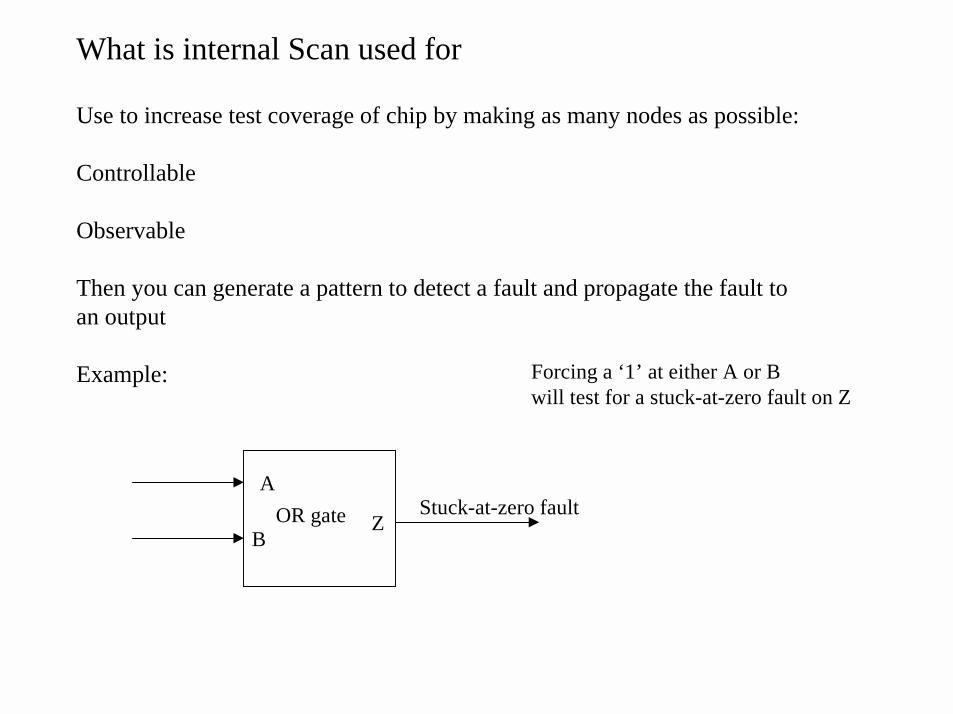
What is internal Scan used for
Use to increase test coverage of chip by making as many nodes as possible:
Controllable
Observable
Then you can generate a pattern to detect a fault and propagate the fault toan output
Example:
OR gate Stuck-at-zero fault
Forcing a ‘1’ at either A or Bwill test for a stuck-at-zero fault on Z
A
BZ

How to Make nodes controllable and observable using scan/test insertion
Make all sequential elements controllable and observable by replacing DFF with ScanFF
Insert test logic to control internal resets, clocks and ram write enables not controllableexternallyExample:
DZ
CK
DCKTITE
Z
Before Scan After Scan
D
CK
MUX DFF
A
BS
QSystem input
TI
TE
CK
System input
D
CK
R
Before testlogic insertionuncontrollablereset
System input
D
CK
R
After test logicinsertion, resetis controllable
ORTest_mode
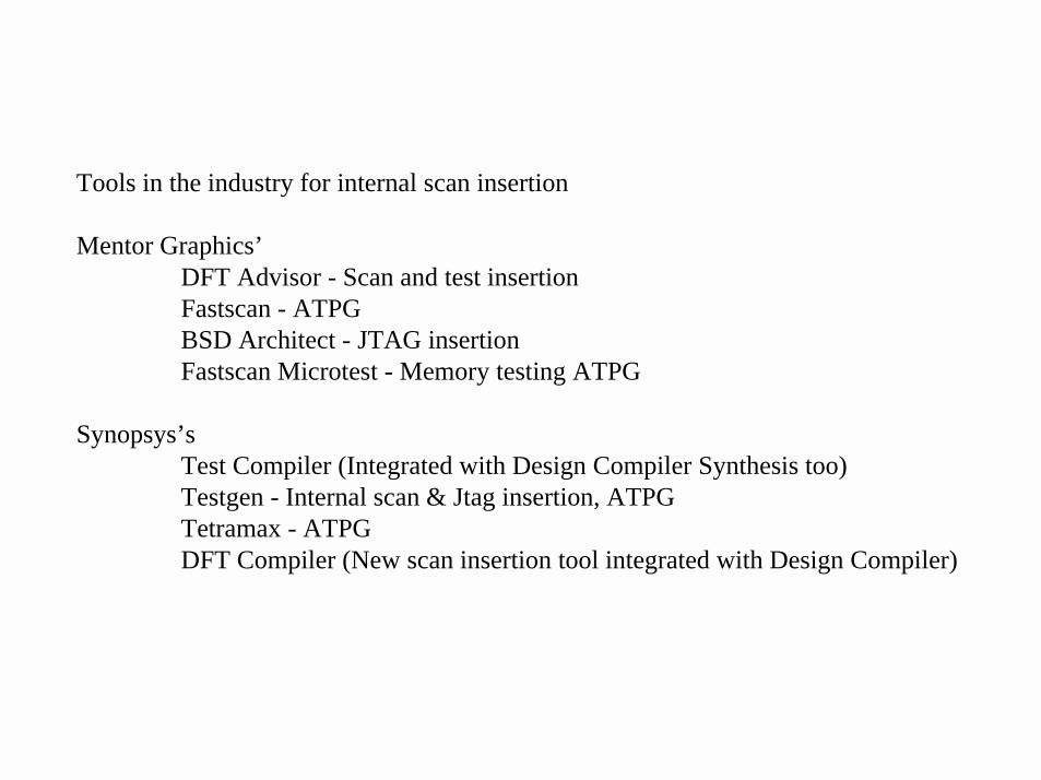
Tools in the industry for internal scan insertion
Mentor Graphics’ DFT Advisor - Scan and test insertionFastscan - ATPGBSD Architect - JTAG insertionFastscan Microtest - Memory testing ATPG
Synopsys’s Test Compiler (Integrated with Design Compiler Synthesis too)Testgen - Internal scan & Jtag insertion, ATPGTetramax - ATPGDFT Compiler (New scan insertion tool integrated with Design Compiler)

INSTRUCTION LATCH DFT ADVISOR DOFILE & TRANSCRIPT
dftadvisor mapped/inst_latch.vhd -vhdl -lib tc240ct.fs_lib -top instr_latch -scripts/instr_dfta.do -nogui // DFTAdvisor v8.6_4.7 Thu Oct 21 15:27:04 PDT 1999// Copyright (c) Mentor Graphics Corporation, 1982-1998, All Rights Reserved.// UNPUBLISHED, LICENSED SOFTWARE.// CONFIDENTIAL AND PROPRIETARY INFORMATION WHICH IS THE// PROPERTY OF MENTOR GRAPHICS CORPORATION OR ITS LICENSORS.////// Mentor Graphics software executing under Sun SPARC SunOS.//// Compiling library ...// Reading VHDL Netlist ...// Elaboration phase ...// Circuit generation phase ...// Cleanup phase ...// command: add clocks 0 /clk // command: set sys mode dft// Flattening process completed, design_cells=160 leaf_cells=160 // library_primitives=288 sim_gates=650 PIs=34 POs=64.// ---------------------------------------------------------------------------// Begin circuit learning analyses.// ---------------------------------------------------------------------------// Equivalent gates=0 classes=0 CPU time=0.00 sec.// Learning completed, implications=0, tied_gates=128, CPU time=0.00 sec.
// ---------------------------------------------------------------------------// Begin scan chain identification process, memory elements = 64.// ---------------------------------------------------------------------------// ---------------------------------------------------------------------------// Begin scannable cell rules checking for 64 nonscan memory elements.// ---------------------------------------------------------------------------// 64 non-scan memory elements identified as scannable.// ---------------------------------------------------------------------------// Begin scan clock rules checking.// ---------------------------------------------------------------------------// 1 scan clock/set/reset lines have been identified.// All scan clocks successfully passed off-state check.// All scan clocks successfully passed capture ability check.// command: run // Number of targeted sequential instances = 64// Performing scan identification ...// Total sequential instances identified = 64// command: insert test logic // Warning: Flattened model has been freed// command: write netlist scan/instr_scan.vhd -vhdl -replace// Writing VHDL netlist ...// command: write atpg setup scripts/instr_scan -replace// command: exit -d21 cascade:/home/cascade_c/laryt/training/vhdl/atpg>
add clocks 0 /clk set sys mode dftrun insert test logic write netlist scan/instr_scan.vhd -vhdl -replacewrite atpg setup scripts/instr_scan -replaceexit -d

INSTRUCTION LATCH FASTSCAN TRANSCRIPT
fastscan scan/instr_scan.vhd -vhdl -lib tc240ct.fs_lib -top instr_latch -dofile scripts/instr_fs.do -nogui -log log/instr_fs.log -replace// FastScan v8.6_4.7 Fri Oct 8 19:35:34 PDT 1999// Copyright (c) Mentor Graphics Corporation, 1982-1998, All Rights Reserved.// UNPUBLISHED, LICENSED SOFTWARE.// CONFIDENTIAL AND PROPRIETARY INFORMATION WHICH IS THE// PROPERTY OF MENTOR GRAPHICS CORPORATION OR ITS LICENSORS.////// Mentor Graphics software executing under Sun SPARC SunOS.//// Compiling library ...// Reading VHDL Netlist ...// Elaboration phase ...// Circuit generation phase ...// Cleanup phase ...// command: dofile scripts/instr_scan.dofile// command: add scan groups grp1 scripts/instr_scan.testproc// command: add scan chains chain1 grp1 scan_in1 CURRENT_INSTR2(0)// command: add clocks 0 CLK// command: set system mode atpg// Flattening process completed, design_cells=160 leaf_cells=160 // library_primitives=352 sim_gates=720 PIs=36 POs=64.// ---------------------------------------------------------------------------// Begin circuit learning analyses.// ---------------------------------------------------------------------------// Equivalent gates=0 classes=0 CPU time=0.00 sec.// Learning completed, implications=0, tied_gates=128, CPU time=0.00 sec.// ---------------------------------------------------------------------------// Begin scan chain identification process, memory elements = 64.// ---------------------------------------------------------------------------// Reading group test procedure file scripts/instr_scan.testproc.// Simulating load/unload procedure in grp1 test procedure file.// Chain = chain1 successfully traced with scan_cells = 64.// ---------------------------------------------------------------------------// Begin scan clock rules checking.// ---------------------------------------------------------------------------// 1 scan clock/set/reset lines have been identified.
// All scan clocks successfully passed off-state check.// All scan clocks successfully passed capture ability check.// Capture clock is set to CLK.// command: add faults -all// command: run// ------------------------------------------------------------------------// Simulation performed for #gates = 720 #faults = 1218// system mode = ATPG pattern source = internal patterns// ------------------------------------------------------------------------// #patterns test #faults #faults # eff. # test process// simulated coverage in list detected patterns patterns CPU time// begin random patterns: capture clock = /CLK, observe point = MASTER// 32 98.94% 17 1201 17 17 0.00 sec// 64 100.00% 0 17 3 20 0.00 sec// command: report stat
Statistics report------------------------------------------- #faults #faultsfault class (coll.) (total)----------------------- ------- -------FU (full) 1220 1608----------------------- ------- -------DS (det_simulation) 834 1218DI (det_implication) 386 390----------------------- ------- -------test_coverage 100.00% 100.00%fault_coverage 100.00% 100.00%atpg_effectiveness 100.00% 100.00%-------------------------------------------#test_patterns 20#simulated_patterns 96CPU_time (secs) 1.6-------------------------------------------
// command: exit -d

DataGenerator
AddressGenerator
Addrress ControlLogic
BISTLogicController
RAM
RAM
MUXSignatureRegister
MEMORY BIST
Test circuitry for generating memory test patterns on-chip and verifying the memory response
Many RAMs can share the same BIST logic to reduce overhead
Data, addresses and control signals are generated simultaneously
Memory outputs are fed to a signature register which provides compressed data used todetermine if the memories are fault free.

TESTGEN JTAG SCAN INSERTION FLOW:1. Create the following files:
TSC: Drives the scan insertionBSR: List and order of signals to insertion boundary scan cellsTPI: Timing information for pattern generatationPINMAP: Needed to generate BSDL file
2. Compile the netlist and insert boundary scan and jtag controllernetcompile cpu_core.vhd -restartlitenetcompile cpu_core.vhd
3. Verify the JTAG logic was inserted correctlydrc -jtagverify
4. Import the JTAG functional test patternstestpat -import cpu_core.jtv
5. Create a target fault list and run the fault-simulation, then report the faults detectedfaultlist -expect faultsim -expectfaultrep -names -detected
6. Write out the test patterns for the tester in TSTL2 formattestpat -tester tstl2

Up and Coming CAD software to reduce the Design time
The most difficult task today is timing closure after layout, usually thecustomer must first synthesize using WLM, simulate then give the design tothe ASIC vendor for layout.
If layout does not meet timing the designer needs to go back and re-synthesize andre-optimize the design to meet timing requirements, then repeat the layout step
Also the inserted test logic (internal scan, jtag, memory BIST) will cause timingsome errors.
Solution: Insert test logic in the synthesis tool and get placement information at the front of the design cycle.
Physical Synthesis Tools: Run synthesis and placement at the same time this produces more realistic timing, WLM can be 30% off
Scan and Jtag insertion are integrated into the synthesis tool, so that the synthesistool can optimize with the jtag and internal scan cells

Test-logic-reset
Run-test-idle Select-dr-scan
Capture-dr
Shift-dr
Exit1-dr
Pause-dr
Exit2-dr
Update-dr
0
0
0
1
0
1
1
Select-ir-scan
Capture-ir
Shift-ir
Exit1-ir
Pause-ir
Exit2-ir
Update-dr
0
0
1
0
1
1
0
0
0
0
1 1
1 1
00
1
01 1 1
1 1 00
TAP Controller State Diagram

TAP CONTROL VHDL CODE
library ieee;use ieee.std_logic_1164.all;
entity tap_control is port(trst, tms, tck: in std_logic;tap_out: out std_logic_vector(8 downto 0));
--reset,enable,select_1,clk_ir,sfir,udir,clk_dr,sfdr,uddrend tap_control;
architecture arch1 of tap_control istype StateType is (test_logic_reset,run_test_idle,select_dr,capture_dr,shift_dr,exit1_dr,pause_dr,exit2_dr,update_dr,select_ir,capture_ir,shift_ir,exit1_ir,pause_ir,exit2_ir,update_ir);signal present_state,next_state : StateType;
beginstate_comb:process(tms,trst,tck,present_state)begin
if (trst = '0') thentap_out <= "000000000";next_state <= test_logic_reset;
else

case present_state iswhen test_logic_reset => tap_out <= "101100100";
if (tms = '0') then next_state <= run_test_idle;elsenext_state <= test_logic_reset; end if;
when run_test_idle => tap_out <= "101100100"; if (tms = '1') then next_state <= select_dr;else next_state <= run_test_idle; end if;
when select_dr => tap_out <= "100100100"; if (tms = '0') then next_state <= capture_dr;elsenext_state <= select_ir; end if;
when capture_dr => tap_out <= "101100100"; if (tms = '0') then next_state <= shift_dr;else next_state <= exit1_dr; end if;
when shift_dr => tap_out <= "110100110"; if (tms = '1') then next_state <= exit1_dr;elsenext_state <= shift_dr; end if;
when exit1_dr => tap_out <= "100100110"; if (tms = '0') then next_state <= pause_dr;else next_state <= update_dr; end if;
when pause_dr => tap_out <= "100100100"; if (tms = '1') then next_state <= exit2_dr;else next_state <= pause_dr; end if;
when exit2_dr => tap_out <= "110100100"; if (tms = '1') then next_state <= update_dr;else next_state <= shift_dr; end if;
when update_dr => tap_out <= "100101100"; if (tms = '1') then next_state <= select_dr;else next_state <= run_test_idle; end if;
Select-dr-scan
Capture-dr
Shift-dr
Exit1-dr
Pause-dr
Exit2-dr
Update-dr
0
0
1
0
1
1
0
0
1
1
0
1
TAP CONTROL VHDL CODE - CONTINUED

when select_ir => tap_out <= "110100100"; if (tms = '0') then next_state <= capture_ir;else next_state <= test_logic_reset; end if;
when capture_ir => tap_out <= "101100100"; if (tms = '0') then next_state <= shift_ir;else next_state <= exit1_ir; end if;
when shift_ir => tap_out <= "111110100"; if (tms = '1') then next_state <= exit1_ir;else next_state <= shift_ir; end if;
when exit1_ir => tap_out <= "100100100"; if(tms = '0') then next_state <= pause_ir;else next_state <= update_ir; end if;
when pause_ir => tap_out <= "101100100"; if (tms = '1') then next_state <= exit2_ir;else next_state <= pause_ir; end if;
when exit2_ir => tap_out <= "111100100"; if (tms = '1') then next_state <= update_ir;else next_state <= shift_ir; end if;
when update_ir => tap_out <= "101101100"; if (tms = '1') then next_state <= select_dr;else next_state <= run_test_idle; end if;
end case; end if;end process state_comb;state_clocked:process(tck) begin
if rising_edge(tck) then present_state <= next_state;end if;
end process state_clocked;end arch1;
Select-ir-scan
Capture-ir
Shift-ir
Exit1-ir
Pause-ir
Exit2-ir
Update-dr
0
0
1
0
1
1
0
0
1
1
0
TAP CONTROL VHDL CODE - CONTINUED

TAP CONTROLLER TESTBENCH: TABULAR APPROACHlibrary ieee;use ieee.std_logic_1164.all;package tap_pkg is
component tap_control port(trst, tms, tck : in std_logic;
tap_out : out std_logic_vector(8 downto 0));end component;
end tap_pkg;library ieee;use ieee.std_logic_1164.all;entity tap_testbench isend tap_testbench;use work.tap_pkg.all;architecture tap_test of tap_testbench is
signal tck,tms,trst : std_logic;signal tap_out : std_logic_vector(8 downto 0);
type test_vector is recordtck,tms,tck,trst : std_logic;
tap_out : std_logic_vector(8 downto 0);end record;type test_vector_array is array(natural range<>) of test_vector;constant test_vectors: test_vector_array := (
-- test_logic_reset(trst => '0', tms => '1', tck => '1', tap_out => "000000000"), -- 0 ns(trst => '0', tms => '1', tck => '0', tap_out => "000000000"), -- 50 ns(trst => '1', tms => '0', tck => '1', tap_out => "101100100"), -- 100 ns(trst => '1', tms => '0', tck => '0', tap_out => "101100100"), -- 150 ns

-- run_test_idle(trst => '1', tms => '1', tck => '1', tap_out => "101100100"), -- 200 ns(trst => '1', tms => '1', tck => '0', tap_out => "101100100"), -- 250 ns-- select_dr(trst => '1', tms => '0', tck => '1', tap_out => "100100100"), -- 300 ns(trst => '1', tms => '0', tck => '0', tap_out => "100100100"), -- 350 ns-- cature_dr(trst => '1', tms => '0', tck => '1', tap_out => "101100100"), -- 400 ns(trst => '1', tms => '0', tck => '0', tap_out => "101100100"), -- 450 ns-- shift_dr(trst => '1', tms => '1', tck => '1', tap_out => "110100110"), -- 500 ns(trst => '1', tms => '1', tck => '0', tap_out => "110100110"), -- 550 ns-- exit1_dr(trst => '1', tms => '0', tck => '1', tap_out => "100100110"), -- 600 ns(trst => '1', tms => '0', tck => '0', tap_out => "100100110"), -- 650 ns-- pause_dr(trst => '1', tms => '1', tck => '1', tap_out => "100100100"), -- 700 ns(trst => '1', tms => '1', tck => '0', tap_out => "100100100"), -- 750 ns-- exit2_dr(trst => '1', tms => '1', tck => '1', tap_out => "110100100"), -- 800 ns(trst => '1', tms => '1', tck => '0', tap_out => "110100100"), -- 850 ns-- update_dr(trst => '1', tms => '1', tck => '1', tap_out => "100101100"), -- 900 ns(trst => '1', tms => '1', tck => '0', tap_out => "100101100"), -- 950 ns-- select_dr(trst => '1', tms => '1', tck => '1', tap_out => "100100100"), --1000 ns(trst => '1', tms => '1', tck => '0', tap_out => "100100100"), --1050 ns
TAP CONTROLLER TESTBENCH: TABULAR APPROACH

-- select_ir(trst => '1', tms => '0', tck => '1', tap_out => "110100100"), --1100 ns(trst => '1', tms => '0', tck => '0', tap_out => "110100100"), --1150 ns-- capture_ir(trst => '1', tms => '0', tck => '1', tap_out => "101100100"), --1200 ns(trst => '1', tms => '0', tck => '0', tap_out => "101100100"), --1250 ns-- shift_ir(trst => '1', tms => '1', tck => '1', tap_out => "111110100"), --1300 ns(trst => '1', tms => '1', tck => '0', tap_out => "111110100"), --1350 ns-- exit1_ir(trst => '1', tms => '0', tck => '1', tap_out => "100100100"), --1400 ns(trst => '1', tms => '0', tck => '0', tap_out => "100100100"), --1450 ns-- pause_ir(trst => '1', tms => '1', tck => '1', tap_out => "101100100"), --1500 ns(trst => '1', tms => '1', tck => '0', tap_out => "101100100"), --1550 ns-- exit2_ir(trst => '1', tms => '1', tck => '1', tap_out => "111100100"), --1600 ns(trst => '1', tms => '1', tck => '0', tap_out => "111100100"), --1650 ns-- update_ir(trst => '1', tms => '0', tck => '1', tap_out => "101101100"), --1700 ns(trst => '1', tms => '0', tck => '0', tap_out => "101101100"), --1750 ns-- run_test_idle(trst => '1', tms => '0', tck => '1', tap_out => "101100100"), --1800 ns(trst => '1', tms => '0', tck => '0', tap_out => "101100100") --1850 ns);
TAP CONTROLLER TESTBENCH: TABULAR APPROACH

beginuut: tap_control port map (tck => tck, trst => trst, tms => tms, tap_out => tap_out);verify: process
variable vector: test_vector;variable errors: boolean := false;
begin for i in test_vectors'range loop
vector := test_vectors(i); tck <= vector.tck;
trst <= vector.trst;tms <= vector.tms;wait for 50 ns;if tap_out /= vector.tap_out then
assert falsereport "output is wrong value";
errors := true;end if;
end loop;assert not errors
report "Test vectors failed"severity Error;
assert errorsreport "Test vectors passed"severity Note;
wait;end process;
end tap_test;
TAP CONTROLLER TESTBENCH: TABULAR APPROACH

TAP CONTROL MODELSIM SIMULATION LIST REPORT
ns /tap_testbench/uut/present_statedelta /tap_testbench/uut/next_state
/tap_testbench/uut/tms/tap_testbench/uut/tck
/tap_testbench/uut/tap_out0 +2 1 1 000000000 test_logic_reset test_logic_reset50 +1 1 0 000000000 test_logic_reset test_logic_reset100 +2 0 1 101100100 test_logic_reset run_test_idle150 +1 0 0 101100100 test_logic_reset run_test_idle200 +3 1 1 101100100 run_test_idle select_dr250 +1 1 0 101100100 run_test_idle select_dr300 +3 0 1 100100100 select_dr capture_dr350 +1 0 0 100100100 select_dr capture_dr400 +3 0 1 101100100 capture_dr shift_dr450 +1 0 0 101100100 capture_dr shift_dr500 +3 1 1 110100110 shift_dr exit1_dr550 +1 1 0 110100110 shift_dr exit1_dr600 +3 0 1 100100110 exit1_dr pause_dr650 +1 0 0 100100110 exit1_dr pause_dr700 +3 1 1 100100100 pause_dr exit2_dr750 +1 1 0 100100100 pause_dr exit2_dr800 +3 1 1 110100100 exit2_dr update_dr850 +1 1 0 110100100 exit2_dr update_dr900 +3 1 1 100101100 update_dr select_dr950 +1 1 0 100101100 update_dr select_dr1000 +21 1 1 100100100 select_dr select_ir

Instruction Latch Block Diagram
instruction
clk
Latch_instr
Current_instr1 Current_instr2
INSTRUCTION LATCH
PROGRAM COUNTERDATAPATHCONTROL
CONTROL
32
32 32

library ieee;use ieee.std_logic_1164.all;entity instr_latch is
generic (instr_size: integer := 32); port ( clk, latch_instr: in std_logic; instr: in std_logic_vector(instr_size-1 downto 0); current_instr1: out std_logic_vector(instr_size-1 downto 0); current_instr2: out std_logic_vector(instr_size-1 downto 0) );end instr_latch;
architecture arch1 of instr_latch isbegin
processbegin
wait until clk'event and clk = '1'; if (latch_instr = '1') then current_instr1 <= instr; current_instr2 <= instr; end if; end process;end arch1;
Instruction Latch VHDL Code

library ieee;use ieee.std_logic_1164.all;package instr_pkgs is component instr_latch
generic (instr_size : integer := 32);port (clk, latch_instr : in std_logic;instr : in std_logic_vector(instr_size-1 downto 0);current_inst1 :out std_logic_vector(instr_size-1 downto 0); current_inst2 : out std_logic_vector(instr_size-1 downto 0));
end component;end instr_pkgs;
library ieee;use ieee.std_logic_1164.all;entity instr_testbench is
generic (instr_size: integer := 32);end instr_testbench;
library ieee;use ieee.std_logic_1164.all;use IEEE.std_logic_signed.all;use IEEE.std_logic_arith.all;use work.instr_pkgs.all;architecture instr_test of instr_testbench is
INSTRUCTION LATCH TESTBENCH: PROCEDURAL APPROACH

component instr_latchport (clk, latch_instr : in std_logic;instr : in std_logic_vector(instr_size-1 downto 0);current_instr1, current_instr2 : out std_logic_vector(instr_size-1 downto 0));
end component;signal clk : std_logic := '0';signal latch_instr : std_logic := '1';signal instr : std_logic_vector(instr_size-1 downto 0) := (others => '0');signal current_instr1, current_instr2 : std_logic_vector(instr_size-1 downto 0);
beginuu1: instr_latch port map (
clk => clk, latch_instr => latch_instr, instr => instr,current_instr1 => current_instr1, current_instr2 => current_instr2);
clk <= not(clk) after 50 ns;verify:processbegin
for i in 0 to 1000 loopwait until clk'event and clk='1' and latch_instr = '1';
current_instr1 <= instr;current_instr2 <= instr;instr <= instr + 1;
end loop;end process;end instr_test;
INSTRUCTION LATCH TESTBENCH: PROCEDURAL APPROACH

INSTRUCTION LATCH MODELSIM SIMULATION OF TESTBENCH
ns /instr_testbench/clkdelta /instr_testbench/instr/instr_testbench/latch_instr
/instr_testbench/current_instr1/instr_testbench/current_instr2
0 +0 0 1 00000000 XXXXXXXX XXXXXXXX50 +1 1 1 00000001 00000000 00000000100 +0 0 1 00000001 00000000 00000000150 +1 1 1 00000002 00000001 00000001200 +0 0 1 00000002 00000001 00000001250 +1 1 1 00000003 00000002 00000002300 +0 0 1 00000003 00000002 00000002350 +1 1 1 00000004 00000003 00000003400 +0 0 1 00000004 00000003 00000003450 +1 1 1 00000005 00000004 00000004500 +0 0 1 00000005 00000004 00000004550 +1 1 1 00000006 00000005 00000005600 +0 0 1 00000006 00000005 00000005650 +1 1 1 00000007 00000006 00000006700 +0 0 1 00000007 00000006 00000006750 +1 1 1 00000008 00000007 00000007800 +0 0 1 00000008 00000007 00000007850 +1 1 1 00000009 00000008 00000008900 +0 0 1 00000009 00000008 00000008950 +1 1 1 0000000A 00000009 000000091000 +21 0 1 0000000A 00000009 00000009

ATPG TEST COVERAGE FOR INSTRUCTION LATCH
Statistics report-------------------------------------------
#faults #faultsfault class (coll.) (total)----------------------- ------- -------FU (full) 1220 1608----------------------- ------- -------DS (det_simulation) 834 1218DI (det_implication) 386 390----------------------- ------- -------test_coverage 100.00% 100.00%fault_coverage 100.00% 100.00%atpg_effectiveness 100.00% 100.00%-------------------------------------------#test_patterns 20#simulated_patterns 96CPU_time (secs) 1.6-------------------------------------------

Datapath Block Diagram
psw_zeropsw_neg
psw_carry
clk
resetZero_flagneg_flagcarry_flag
reset_aluread_aread_bsel_instr_or_bsel_instr_or_alulatch_flags
alu_a alu_b
ALUREGFILE
reg_a reg_b reg_c addr_a
CONTROL
alu_zeroalu_neg
alu_carryalu_result
STACK
current_instruction
INSTRUCTION_LATCH
DATAPATH
32
16 1616 16
16 716

DATAPATH VHDL CODE (Entity)
library ieee;use ieee.std_logic_1164.all;entity datapath is
generic (instr_size: integer := 32; data_size: integer := 16);
port ( clk, reset, reset_alu, read_a, read_b: in std_logic; sel_instr_or_b, sel_instr_or_alu: in std_logic; reg_a, reg_b, alu_result: in std_logic_vector(data_size-1 downto 0); current_instr: in std_logic_vector(instr_size-1 downto 0); latch_flags, alu_zero, alu_neg, alu_carry: in std_logic; psw_zero, psw_neg, psw_carry: in std_logic; zero_flag, neg_flag, carry_flag: out std_logic; alu_a, alu_b, reg_c: out std_logic_vector(data_size-1 downto 0) );end datapath;

architecture arch1 of datapath is signal pswl_zero, pswl_carry, pswl_neg: std_logic;begin process begin wait until clk'event and clk = '1'; -- either reset the alu output or transfer reg_a to alu_a if (reset_alu = '1') then alu_b <= (others => '0'); elsif (read_a = '1') then alu_a <= reg_a; end if; if (reset_alu = '1') then alu_b <= (others => '0'); elsif (read_b = '1') then alu_b <= reg_b; elsif (sel_instr_or_b = '1') then alu_b <= "00000000" & current_instr(7 downto 0); end if;
if (reset = '1') then pswl_zero <= '0'; pswl_neg <= '0'; pswl_carry <= '0'; else pswl_zero <= psw_zero; pswl_neg <= psw_neg; pswl_carry <= psw_carry; end if; end process;
DATAPATH VHDL CODE - continued

-- Mux alu_result and current_instr data to reg_c process (current_instr, alu_result, sel_instr_or_alu) begin if (sel_instr_or_alu = '1') then
reg_c <= current_instr(data_size-1 downto 0); else
reg_c <= alu_result; end if; end process;
-- Mux flags bwt popped and alu outputs -- Return instrn alone requires popped flags process(current_instr, pswl_zero, pswl_neg, pswl_carry, alu_zero, alu_neg, alu_carry) begin if (current_instr(instr_size-1 downto 24) = "00001000") then zero_flag <= pswl_zero; neg_flag <= pswl_neg; carry_flag <= pswl_carry; else zero_flag <= alu_zero; neg_flag <= alu_neg; carry_flag <= alu_carry; end if; end process;end arch1;
DATAPATH VHDL CODE - continued

ATPG TEST COVERAGE FOR DATAPATH
Statistics report-------------------------------------------
#faults #faultsfault class (coll.) (total)----------------------- ------- -------FU (full) 956 1340----------------------- ------- -------DS (det_simulation) 640 1022DI (det_implication) 214 216UU (unused) 88 88AU (atpg_untestable) 14 14----------------------- ------- -------test_coverage 98.39% 98.88%fault_coverage 89.33% 92.39%atpg_effectiveness 100.00% 100.00%-------------------------------------------#test_patterns 34#simulated_patterns 288CPU_time (secs) 1.5-------------------------------------------

REGISTER FILE BLOCK DIAGRAM
INSTRUCTION LATCH
DATAPATH
Addr_A Addr_B
clkreset
write_reg_creg_a reg_b
CONTROLAddr_C Reg_C
REGISTER FILE
7 7
716 16 16

REGISTER FILE VHDL CODE
library ieee;use ieee.std_logic_1164.all;
entity regfile is generic (addr_size: integer := 6; data_size: integer := 16); port ( clk,reset: in std_logic; write_c: in std_logic; reg_c: in std_logic_vector(data_size-1 downto 0); addr_a: in std_logic_vector(addr_size-1 downto 0); addr_b: in std_logic_vector(addr_size-1 downto 0); addr_c: in std_logic_vector(addr_size-1 downto 0); reg_a, reg_b: out std_logic_vector(data_size-1 downto 0) );end regfile;

architecture arch1 of regfile is type regfile is array (0 to 3) of std_logic_vector(data_size-1 downto 0); signal reg_array: regfile;begin process begin wait until clk'event and clk = '1'; if (reset = '1') then for i in 0 to 3 loop reg_array(i) <= (others => '0'); end loop; end if; if (write_c = '1') then reg_array(conv_integer(unsigned(addr_c(1 downto 0)))) <= reg_c; end if; end process; process (addr_a, reg_array) begin reg_a <= reg_array(conv_integer(unsigned(addr_a(1 downto 0)))); end process; process (addr_b, reg_array) begin reg_b <= reg_array(conv_integer(unsigned(addr_b(1 downto 0)))); end process;end arch1;
REGISTER FILE VHDL CODE - CONTINUED

ATPG TEST COVERAGE FOR REGFILE
Statistics report-------------------------------------------
#faults #faultsfault class (coll.) (total)----------------------- ------- -------FU (full) 1840 2624----------------------- ------- -------DS (det_simulation) 1299 2081DI (det_implication) 388 390UU (unused) 152 152RE (redundant) 1 1----------------------- ------- -------test_coverage 100.00% 100.00%fault_coverage 91.68% 94.17%atpg_effectiveness 100.00% 100.00%-------------------------------------------#test_patterns 46#simulated_patterns 224CPU_time (secs) 1.8-------------------------------------------

ALU BLOCK DIAGRAM
alu_a alu_b alu_resultclkresetalu_ctrl
latch_resultlatch_flag
zero_flagneg_flag
carry_flag
DATAPATH
INSTR_LATCHDATAPATH
CONTROL

ALU_CTRL FUNCTION NAME OPERATION------------------------------------------------------------------------------------00000 OP_ADD A + B000001 OP_ADD_PLUS_ONE A + B + 1 000010 OP_A A000011 OP_A_PLUS_ONE A + 1 010001 OP_A_AND_B A & B010010 OP_NOT_A_AND_B !A & B 010011 OP_B B011000 OP_NOT_A_AND_NOT_B !A & !B011001 OP_A_XNOR_B A xnor B011010 OP_NOT_A !A011011 OP_NOT_A_OR_B !A | B 000100 OP_SUB_MINUS_ONE A - B - 1000101 OP_SUB A - B000110 OP_A_MINUS_ONE A - 1010100 OP_A_AND_NOT_B A & !B010110 OP_A_XOR_B A XOR B010111 OP_A_OR_B A | B011100 OP_NOT_B !B011101 OP_A_OR_NOT_B A | !B011110 OP_A_NAND_B A NAND B010000 OP_ALL_ZEROS ‘0’011111 OP_ALL_ONES ‘1’
ALU TRUTH TABLE

ALU PACKAGE VHDL CODElibrary ieee;use ieee.std_logic_1164.all;package alu_pkgs is
-- ALU functionsconstant op_add : std_logic_vector(5 downto 0) := "000000"; constant op_add_plus_one : std_logic_vector(5 downto 0) := "000001"; constant op_a : std_logic_vector(5 downto 0) := "000010"; constant op_a_plus_one : std_logic_vector(5 downto 0) := "000011"; constant op_a_and_b : std_logic_vector(5 downto 0) := "010001";
constant op_nota_and_b : std_logic_vector(5 downto 0) := "010010"; constant op_b : std_logic_vector(5 downto 0) := "010011"; constant op_nota_and_notb : std_logic_vector(5 downto 0) := "011000"; constant op_a_xnor_b : std_logic_vector(5 downto 0) := "011001"; constant op_nota : std_logic_vector(5 downto 0) := "011010"; constant op_nota_or_b : std_logic_vector(5 downto 0) := "011011"; constant op_sub_minus_one : std_logic_vector(5 downto 0) := "000100"; constant op_sub : std_logic_vector(5 downto 0) := "000101"; constant op_a_minus_one : std_logic_vector(5 downto 0) := "000110"; constant op_a_and_notb : std_logic_vector(5 downto 0) := "010100"; constant op_a_xor_b : std_logic_vector(5 downto 0) := "010110"; constant op_a_or_b : std_logic_vector(5 downto 0) := "010111"; constant op_notb : std_logic_vector(5 downto 0) := "011100"; constant op_a_or_notb : std_logic_vector(5 downto 0) := "011101"; constant op_a_nand_b : std_logic_vector(5 downto 0) := "011110";
constant op_all_zeros : std_logic_vector(5 downto 0) := "010000";constant op_all_ones : std_logic_vector(5 downto 0) := "011111";
end alu_pkgs;

ALU VHDL CODElibrary ieee;use ieee.std_logic_1164.all;use IEEE.std_logic_signed.all;use IEEE.std_logic_arith.all;use work.alu_pkgs.all;
entity alu is -- Generic data_size allows the user to easily change the data_size of the alu
generic (data_size: integer := 16);port( clk,reset : in std_logic;
alu_a, alu_b : in std_logic_vector(data_size-1 downto 0);alu_ctrl : in std_logic_vector(5 downto 0);latch_result, latch_flag : in std_logic;alu_result : out std_logic_vector(data_size-1 downto 0);zero_flag, neg_flag, carry_flag : out std_logic);
end alu;architecture arch1 of alu is
signal op_result, result : std_logic_vector(data_size-1 downto 0);signal alu_zero, alu_carry,signal alu_neg : std_logic;
beginalu: process (alu_a, alu_b, alu_ctrl)
begincase alu_ctrl is
when op_add => result <= alu_a + alu_b;when op_add_plus_one => result <= alu_a + alu_b + '1';when op_a => result <= alu_a;

ALU VHDL CODE: CONTINUED
when op_a_plus_one => result <= alu_a + '1';when op_a_and_b => result <= alu_a and alu_b ;when op_nota_and_b => result <= not alu_a and alu_b ;when op_b => result <= alu_b;when op_nota_and_notb => result <= not alu_a and not alu_b ;when op_a_xnor_b => result <= not (alu_a xor alu_b) ;when op_nota => result <= not alu_a;when op_nota_or_b => result <= not alu_a or alu_b ;when op_sub_minus_one => result <= alu_a -alu_b - '1';when op_sub => result <= alu_a - alu_b;when op_a_minus_one => result <= alu_a - '1';when op_a_and_notb => result <= alu_a and not alu_b ;when op_a_xor_b => result <= alu_a xor alu_b ;when op_a_or_b => result <= alu_a or alu_b ;when op_notb => result <= not alu_b;when op_a_or_notb => result <= alu_a or not alu_b ;when op_a_nand_b => result <= alu_a nand alu_b ;when op_all_zeros => result <= (others => '0') ;when op_all_ones => result <= (others => '1') ;when others => result <= (others => '0') ;end case;
if (result = 0) then alu_zero <= '1';else alu_zero <= '0';end if;if (result < 0) then alu_neg <= '1';else alu_neg <= '0';end if;alu_carry <= '0';op_result <= result;end process;
processbeginwait until clk'event and clk = '1';if (latch_result = '1') then
alu_result <= op_result;end if;if (reset = '1') then
zero_flag <= '0';neg_flag <= '0';carry_flag <= '0';
elsif (latch_flag = '1') thenzero_flag <= alu_zero;neg_flag <= alu_neg;carry_flag <= alu_carry;
end if;end process;end arch1;

ALU TESTBENCH VHDL: PROCEDURAL APPROACH
library ieee;use ieee.std_logic_1164.all;package alu1_pkgs is
component alu generic ( data_size : integer := 16); port ( clk, reset : in std_logic;
alu_a, alu_b : in std_logic_vector(data_size-1 downto 0); alu_ctrl : in std_logic_vector(5 downto 0);
latch_result, latch_flag : in std_logic; alu_result : out std_logic_vector(data_size-1 downto 0);
zero_flag ,neg_flag, carry_flag : out std_logic); end component;end alu1_pkgs;
library ieee;use ieee.std_logic_1164.all;entity alu_testbench is
generic ( data_size : integer := 16;no_of_vectors : integer := 76);
end alu_testbench;
library ieee;use ieee.std_logic_1164.all;use IEEE.std_logic_signed.all;use IEEE.std_logic_arith.all;use work.alu_pkgs.all;use work.alu1_pkgs.all;architecture alu_test of alu_testbench is

component alu port(clk,reset,latch_result,latch_flag : in std_logic;
alu_a, alu_b : in std_logic_vector(data_size-1 downto 0); alu_ctrl : in std_logic_vector(5 downto 0); alu_result : out std_logic_vector(data_size-1 downto 0);
zero_flag , neg_flag, carry_flag: out std_logic);end component;
signal alu_a, alu_b : std_logic_vector(data_size-1 downto 0) := (others => '0'); signal alu_result : std_logic_vector(data_size-1 downto 0); signal alu_ctrl : std_logic_vector(5 downto 0) := "000000"; signal clk.\,reset : std_logic := '0'; signal latch_result, latch_flag : std_logic := '1';
signal zero_flag, neg_flag, carry_flag : std_logic;signal temp : std_logic_vector(data_size*2-1 downto 0) := (others => '0');
beginuu1: alu port map (clk=>clk, reset=>reset, alu_a=>alu_a, alu_b=>alu_b,alu_ctrl=>alu_ctrl,latch_result=>latch_result, latch_flag =>latch_flag,alu_result =>alu_result,zero_flag =>zero_flag,neg_flag =>neg_flag,carry_flag =>carry_flag);clk <= not(clk) after 50 ns;verify: processbegin
for j in 0 to 3 loopfor i in 0 to no_of_vectors loop
wait until clk'event and clk='1';alu_a <= temp(data_size*2-1 downto data_size);alu_b <= temp(data_size-1 downto 0);temp <= temp + 1;
end loop;alu_ctrl <= alu_ctrl + 1;
end loop;end process; end alu_test;

ALU MODELSIM SIMULATION OF TESTBENCH
ns /alu_testbench/alu_a /alu_testbench/clk /alu_testbench/neg_flag
delta /alu_testbench/alu_b /alu_testbench/latch_result /alu_testbench/temp/alu_testbench/alu_result /alu_testbench/latch_flag
/alu_testbench/alu_ctrl /alu_testbench/zero_flag/alu_testbench/reset /alu_testbench/carry_flag
0 +0 0 0 X 000000 0 0 1 1 U U U 050 +1 0 0 X 000000 1 0 1 1 0 0 0 1
100 +0 0 0 X 000000 0 0 1 1 0 0 0 1150 +1 0 1 X 000000 1 0 1 1 0 0 0 2200 +0 0 1 X 000000 0 0 1 1 0 0 0 2250 +1 0 2 0 000000 1 0 1 1 1 0 0 3300 +0 0 2 0 000000 0 0 1 1 1 0 0 3350 +1 0 3 1 000000 1 0 1 1 0 0 0 4400 +0 0 3 1 000000 0 0 1 1 0 0 0 4450 +1 0 4 2 000000 1 0 1 1 0 0 0 5500 +0 0 4 2 000000 0 0 1 1 0 0 0 5550 +1 0 5 3 000000 1 0 1 1 0 0 0 6600 +0 0 5 3 000000 0 0 1 1 0 0 0 6650 +1 0 6 4 000000 1 0 1 1 0 0 0 7700 +0 0 6 4 000000 0 0 1 1 0 0 0 7750 +1 0 7 5 000000 1 0 1 1 0 0 0 8800 +0 0 7 5 000000 0 0 1 1 0 0 0 8850 +1 0 8 6 000000 1 0 1 1 0 0 0 9900 +0 0 8 6 000000 0 0 1 1 0 0 0 9950 +1 0 9 7 000000 1 0 1 1 0 0 0 10
1000 +21 0 9 7 000000 0 0 1 1 0 0 0 10

Statistics report-------------------------------------------
#faults #faultsfault class (coll.) (total)----------------------- ------- -------FU (full) 1924 3288----------------------- ------- -------DS (det_simulation) 1798 3160DI (det_implication) 118 120UU (unused) 6 6RE (redundant) 2 2----------------------- ------- -------test_coverage 100.00% 100.00%fault_coverage 99.58% 99.76%atpg_effectiveness 100.00% 100.00%-------------------------------------------#test_patterns 83#simulated_patterns 83CPU_time (secs) 6.2-------------------------------------------
ATPG TEST COVERAGE ALU