mb39a105evb-02 · 2004-05-20 · fujitsu assp product power management 3/23 mb39a105evb-02...
TRANSCRIPT

Fujitsu ASSP Product
1/23Power Management
MB39A105EVB-02 Evaluation Board Rev 1.0
Rev 1.0EApril, 2003
MB39A105EVBMB39A105EVB--0202
Evaluation board ManualEvaluation board Manual

Fujitsu ASSP Product
2/23Power Management
MB39A105EVB-02 Evaluation Board Rev 1.0
MB39A105 Evaluation board MB39A105 Evaluation board
1. 1. EVALUATION BOARD DESCRIPTIONEVALUATION BOARD DESCRIPTION2. 2. EVALUATION BOARD SPECIFICATIONSEVALUATION BOARD SPECIFICATIONS3. 3. TERMINAL DESCRIPTIONTERMINAL DESCRIPTION4. 4. SWITCH DESCRIPTIONSWITCH DESCRIPTION5. 5. SETUP AND CHECKUPSETUP AND CHECKUP6. 6. COMPONENT LAYOUTCOMPONENT LAYOUT7. 7. CONNECTION DIAGRAMCONNECTION DIAGRAM8. 8. PARTS LIST PARTS LIST 9. 9. INITIAL SETTINGSINITIAL SETTINGS10. 10. REFERENCE DATAREFERENCE DATA11. 11. COMPONENT SELECTION METHODSCOMPONENT SELECTION METHODS12. 12. ORDERING INFORMATIONORDERING INFORMATION
MB39A105EVBMB39A105EVB--02 type 02 type

Fujitsu ASSP Product
3/23Power Management
MB39A105EVB-02 Evaluation Board Rev 1.0
1. 1. EVALUATION BOARD DESCRIPTIONEVALUATION BOARD DESCRIPTION
MB39A105EVB-02 is surface mounting circuit board of three system output by which a high voltage and the negative voltage output voltage of a low load are added. When MB39A105 was used, it added the charge pump circuit for the LCD panel.
Vo-2 and Vo-3 are output according to the output voltage of Vo-1. If an optional Zener diode is newly added to ZD1-4, a setting voltage can be adjusted.

Fujitsu ASSP Product
4/23Power Management
MB39A105EVB-02 Evaluation Board Rev 1.0
2.2. EVALUATION BOARD SPECIFICATIONSEVALUATION BOARD SPECIFICATIONS
Input voltageOscillation frequencyOutput voltage 9.0
Output current 120
Output ripple voltage 180
2.4500
3.3. TERMINAL DESCRIPTIONTERMINAL DESCRIPTION
Symbol Descriptions
1 VIN Source and IC driving power-supply terminal
Main GND terminalSGND
4 Vo-1,2,3
Power supply control terminal
VCTL = 0V to 0.4V : Standby modeVCTL = 1.3V to VIN : Operation mode
2
3 PGND1,2
CTL
Output terminal
5
DC/DC converter GND terminal
Soft-start time 10Short-circuit detection time 50
Min Typ Max Unit3.3 4.0 V
kHz400 600
V8.8 9.2
250mA
200
mV--msms
6.1 20.416.9 137.5
VB6 Vo-2 Output voltage setting terminal
Vo-1Vo-2Vo-3
Vo-3Vo-2Vo-1
5-2
25-6.5
--
--
--
--

Fujitsu ASSP Product
5/23Power Management
MB39A105EVB-02 Evaluation Board Rev 1.0
4.4. SWITCH DESCRIPTIONSWITCH DESCRIPTION
SWITCH FUNCTION ON OFF
SW1 Power supply control L (Standby)H (Operating)
(1) Setup
• Power-supply terminals into the VIN and GND terminals.
• Connect the OUT terminal to a required loading device or measuring instrument.
• Set SW1 to OFF.
(2) Checkup
• Set SW1 to ON to supply power to the VIN terminal. When the output voltage is Vo-1=9V(Typ), Vo-2=25V(5mA),and Vo-3=-6.5V(-2mA),the IC is operating normally.
5.5. SETUP AND CHECKUPSETUP AND CHECKUP
Fujitsu ASSP Product
6/23Power Management
MB39A105EVB-02 Evaluation Board Rev 1.0
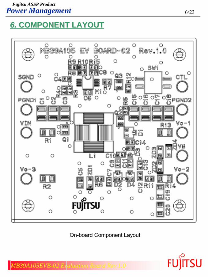
6.6. COMPONENT LAYOUTCOMPONENT LAYOUT
On-board Component Layout

Fujitsu ASSP Product
7/23Power Management
MB39A105EVB-02 Evaluation Board Rev 1.0
Board Layout
Top Side
Bottom Side

Fujitsu ASSP Product
8/23Power Management
MB39A105EVB-02 Evaluation Board Rev 1.0
VIN
(V)
P-G
ND
1 2 3 45678
P-G
ND
M1
Q1
MB3
9A10
5FB
CSC
P
VCC
SCPO
D
-INE
RT
GN
D
OU
T
Vo-3
(-V)
S-G
ND
CTL
Vo-1
(V)
Vo-2
(V)
C1
C2
(C3)
C4
C5
C6
C7C8
C9
C10 C
11
C12
C13C14
C15
C16
C17
C19
C20
R1
R2
R3 R4
R5 R
6
R7R
8
R13
R9
R10 R
11
R12
Q3
Q2
D1
D2
D3
(ZD
1)
D4
(ZD
2)(Z
D3)
(ZD
4)
L1
R14
VIN
(SW
1)
VB
R15
(C18
)
7.7. CONNECTION DIAGRAMCONNECTION DIAGRAM

Fujitsu ASSP Product
9/23Power Management
MB39A105EVB-02 Evaluation Board Rev 1.0
8.8. PARTS LISTPARTS LISTPart No. Part name Specification Manufacturer Package Model name NoteM1 IC MB39A105 FUJITSU FPT-08P-M05 MB39A105PFVQ1 P-ch FET VDS=-20V,ID=4A(Max) SANYO MCPH6 MCH6305Q2,3 N-ch FET VDS=20V,Qg=8.7nC(Typ) SANYO MCPH6 MCH6401D1 Diode VF=0.40V(Max),at IF=1A SANYO CPH3 SBS004D2,3,4 Diode VF=0.44V(Max),at IF=0.1A Origin 3216type F01JD2EZD1 Zener Diode Not mountedZD2 Zener Diode Not mountedZD3 Zener Diode Not mountedZD4 Zener Diode Not mountedL1 Inductor 6.2uH,DCR=62mΩ,1.49A TOKO D62LCB A918CY-6R2MC1 NeoCapacitor 4.7uF(10V) NEC/TOKIN 3225type TEPSLA21A475M8RC2 NeoCapacitor 4.7uF(10V) NEC/TOKIN 3225type TEPSLA21A475M8RC3 Not mountedC4 Ceramic condenser 0.22uF(16V) TDK 1608type C1608JB1C224KC5 Ceramic condenser 1uF(16V) TDK 2012type C2012JB1C105KC6 Ceramic condenser 0.1uF(50V) TDK 1608type C1608JB1H104KC7 Ceramic condenser 0.1uF(50V) TDK 1608type C1608JB1H104KC8 Ceramic condenser 0.1uF(50V) TDK 1608type C1608JB1H104KC9 Ceramic condenser 0.1uF(50V) TDK 1608type C1608JB1H104KC10 Ceramic condenser 0.1uF(50V) TDK 1608type C1608JB1H104KC11 Ceramic condenser 0.1uF(50V) TDK 1608type C1608JB1H104KC12 Ceramic condenser 0.1uF(50V) TDK 1608type C1608JB1H104KC13 Ceramic condenser 0.1uF(50V) TDK 1608type C1608JB1H104KC14 Ceramic condenser 0.1uF(50V) TDK 1608type C1608JB1H104KC15 NeoCapacitor 4.7uF(10V) NEC/TOKIN 3225type TEPSLA21A475M8RC16 NeoCapacitor 4.7uF(10V) NEC/TOKIN 3225type TEPSLA21A475M8RC17 NeoCapacitor 4.7uF(10V) NEC/TOKIN 3225type TEPSLA21A475M8RC18 Not mountedC19 Ceramic condenser 1uF(50V) TDK 3216type C2012JF1H105ZC20 Ceramic condenser 1uF(50V) TDK 3216type C2012JF1H105ZR1 Jumper 0Ω(2A) KOA 3216type RK73Z2BR2 Jumper 0Ω(2A) KOA 3216type RK73Z2BR3 Resistor 100kΩ(0.5%) KOA 1608type RK73G1J104DR4 Jumper 0Ω(1A) KOA 1608type RK73Z1JR5 Jumper 0Ω(1A) KOA 1608type RK73Z1JR6 Resistor 1kΩ(0.5%) KOA 1608type RK73G1J102DR7 Resistor 7.5kΩ(0.5%) KOA 1608type RK73G1J752DR8 Resistor 51kΩ(0.5%) KOA 1608type RK73G1J513DR9 Resistor 22kΩ(0.5%) KOA 1608type RK73G1J223DR10 Resistor 330kΩ(0.5%) KOA 1608type RK73G1J334DR11 Resistor 200Ω(0.5%) KOA 1608type RK73G1J201DR12 Resistor 100kΩ(0.5%) KOA 1608type RK73G1J104DR13 Jumper 0Ω(2A) KOA 3216type RK73Z2BR14 Jumper 0Ω(2A) KOA 3216type RK73Z2BR15 Resistor 43kΩ(0.5%) KOA 1608type RK73G1J433DSW1 DIP switch 2 pole Not mountedPin Terminal pin ST-3-2 MacEight ST-3-2

Fujitsu ASSP Product
10/23Power Management
MB39A105EVB-02 Evaluation Board Rev 1.0
Vo1 (V) = 0.5 / R9 (R10 + R15 + R9) 9.0 (V)
(1) Output voltage
(3) Soft-start time
(2) Oscillation frequency
fosc (kHz) = 3750 / R7(k) 500 (kHz)
ts (s) = 0.045 C4 (uF) 10.0 (ms)
(4) Short-circuit detection time
tscp (s) = 0.23 C4 (uF) 50.0 (ms)
9.9. INITIAL SETTINGSINITIAL SETTINGS
Vo2 (V) = Vo1 + (Vo1 2) - (VF 2 + R11 Io2) 25(V)
Vo3 (V) = - (Vo1 1) - (- VF - R6 Io3) -6.5 (V)
* Io2=5mA, Io3=2mA, VF 0.44V

Fujitsu ASSP Product
11/23Power Management
MB39A105EVB-02 Evaluation Board Rev 1.0
Output voltage Vo1 - Load current Io1
8.908.928.948.968.989.009.029.049.069.089.10
0.01 0.10 1.00
Load current Io1(A)
Out
put
Vol
tage
Vo1
(V)
Total conversion efficiency - Load current
75
80
85
90
95
0.01 0.10 1.00
Load current Io1(A)
Tota
l con
vers
ion
effic
ency
(%)
10.10. REFERENCE DATAREFERENCE DATA(1) (1) Conversion efficiency vs. load current characteristic (VIN = 3.3 V)
(2) Load regulation (VIN = 3.3 V)
VIN=3.3VSetting Vo-1= 9VSetting Vo-2= 25V( 5mA) Setting Vo-3= -6.5V(2mA)
VIN=3.3V
Setting Vo-1=9V
Load Regulation
Vo-1=4.2mV

Fujitsu ASSP Product
12/23Power Management
MB39A105EVB-02 Evaluation Board Rev 1.0
Output voltage Vo-1 - Input voltage
8.90
8.95
9.00
9.05
9.10
2.0 2.5 3.0 3.5 4.0 4.5
Input voltage(V)
Out
put v
olta
ge V
o1(V
)
Setting Vo-1=9V
Io-1=200mA
Output voltage Vo-2 - Input voltage
24.50
24.75
25.00
25.25
25.50
2.0 2.5 3.0 3.5 4.0 4.5
Input voltage(V)
Out
put v
olta
ge V
o2(V
)
Setting Vo-2=25V
Io-2=5mA
Output voltageVO-3 - Input voltage
-6.60
-6.55
-6.50
-6.45
-6.40
2.0 2.5 3.0 3.5 4.0 4.5
Input voltage(V)
Out
put v
olta
ge V
o3(V
)
(3) (3) Line regulationLine regulation
Setting Vo-3= -6.5V
Io-3= -2mA
Line Regulation=11.7mV
Line Regulation=65.6mV
Line Regulation=7.7mV

Fujitsu ASSP Product
13/23Power Management
MB39A105EVB-02 Evaluation Board Rev 1.0
(4) (4) SoftSoft--start operation waveformsstart operation waveforms
Vo-1
Vo-2
Vo-3
2 4 6 8 10 12 14 16 18 20(ms)
50Vo-2(V)
0
2
4
0
10
20
30
40
CTL(V)
Vo-1
Vo-2
Vo-3
CTL CTL
CTL CTL
CTL CTL
2 4 6 8 10 12 14 16 18 20(ms)0
Vo-1(V)
0
2
4
0
2
4
6
8
CTL(V)
1010Vo-1(V)
0
2
4
0
2
4
6
8
CTL(V)
0
50Vo-2(V)
0
2
4
0
10
20
30
40
CTL(V)
2Vo-3(V)
0
2
4
-8
-6
-4
-2
CTL(V)
0
2Vo-3(V)
0
2
4
-8
-6
-4
-2
CTL(V)
0
2 4 6 8 10 12 14 16 18 20(ms)0 2 4 6 8 10 12 14 16 18 20(ms)0
2 4 6 8 10 12 14 16 18 20(ms)0 2 4 6 8 10 12 14 16 18 20(ms)0
VIN=3.3VSetting Vo-1=9VLoad=200mA
VIN=3.3VSetting Vo-1=9VLoad=200mA
VIN=3.3VSetting Vo-2=25VLoad=5mA
VIN=3.3VSetting Vo-2=25VLoad=5mA
VIN=3.3VSetting Vo-3=-6.5VLoad=2mA
VIN=3.3VSetting Vo-3=-6.5VLoad=2mA

Fujitsu ASSP Product
14/23Power Management
MB39A105EVB-02 Evaluation Board Rev 1.0
5.5.Output ripple waveforms (VOutput ripple waveforms (VININ = 3.3 V)= 3.3 V)
a: Voa: Vo--11
b: Vob: Vo--22
0 0.5 1.0 1.5 2.0 2.5 3.0 3.5 4.0 4.5 5.0 (s)
0 0.5 1.0 1.5 2.0 2.5 3.0 3.5 4.0 4.5 5.0 (s)
0
0
-20
-40
20
40Vo-1(mV)
5
10VD(V)
0
0
-20
-40
20
40Vo-2(mV)
5
10VD(V)
VIN=3.3VSetting Vo-1=9VLoad=200mA
VIN=3.3VSetting Vo-2=25VLoad=5mA
Ripple=41mV
Ripple=5.2mV

Fujitsu ASSP Product
15/23Power Management
MB39A105EVB-02 Evaluation Board Rev 1.0
6.6.Short-circuit detection operation waveforms
0 20 40 60 80 100 120 140 160 180 200(ms)
0
0
0
5
5
1.0
0.5
CSCP(V)
Vo (V)
Nch Drain(V)
VIN=3.3VSetting Vo-1=9VVo
Nch Drain
CSCP
c: Voc: Vo--33
0
0
-20
-40
20
40Vo-3(mV)
5
10VD(V)
0 0.5 1.0 1.5 2.0 2.5 3.0 3.5 4.0 4.5 5.0 (s)
VIN=3.3VSetting Vo-3=-6.5VLoad=2mA
Ripple=3.6mV
5.5.Output ripple waveforms (VOutput ripple waveforms (VININ = 3.3 V)= 3.3 V)

Fujitsu ASSP Product
16/23Power Management
MB39A105EVB-02 Evaluation Board Rev 1.0
0 5 10 15 20 25 30 35 40 45 50(ms)
0 5 10 15 20 25 30 35 40 45 50(ms)
a: Voa: Vo--11
b: Vob: Vo--22
0
300
0
1
-1
200
100
Io-1(mA)
Vo-1 (V)
-2
2
0
300
0
1
-1
200
100
Io-1(mA)
Vo-2 (V)
-2
2
VIN=3.3VSetting Vo-1=9VLoad=45
VIN=3.3VSetting Vo-2=25VLoad=5k
(7) (7) Output waveform at load sudden changeOutput waveform at load sudden change(V(VININ=3.3V)=3.3V)

Fujitsu ASSP Product
17/23Power Management
MB39A105EVB-02 Evaluation Board Rev 1.0
0 5 10 15 20 25 30 35 40 45 50(ms)
c: Voc: Vo--33
0
300
0
1
-1
200
100
Io-1(mA)
Vo-3 (V)
-2
2VIN=3.3VSetting Vo-3=-6.5VLoad=3k
(7) (7) Output waveform at load sudden changeOutput waveform at load sudden change(V(VININ=3.3V)=3.3V)

Fujitsu ASSP Product
18/23Power Management
MB39A105EVB-02 Evaluation Board Rev 1.0
11.11. COMPONENT SELECTION METHODSCOMPONENT SELECTION METHODS
Board Photograph
Input Pch FET
Inductor
Flyback diode
Output smoothing capacitor
FET
Diode

Fujitsu ASSP Product
19/23Power Management
MB39A105EVB-02 Evaluation Board Rev 1.0
Vin=2.4V(Min),Vo=9.0V,Io=260mA,fosc=500kHz
(1) N-ch MOS FET(MCH6401(SANYO product) )VDS=20V, VGS=±10V, ID=4A, RDS(on)=45mΩ(Typ), Qg=12nC(Typ)
Vin (Min)
2L ton
-6
ID
Drain current: Peak valueThe peak drain current of this FET must be within its rated current.If the FET’s peak drain current is ID, it is obtained by the following formula.
1.26A
The following subsections show the component selection methods with the following common parametric values.
Vo × IoVin (Min)
+ ton = VoVo- Vin
t
2.4 ×(9 - 2.4)
2 × 6.2 × 10 × 9
9 × 0.262.4
+ ×500 × 10 3
1
(2) P-ch MOS FET(MCH6305(SANYO product) )VDS=-20V, VGS=±10V, ID=4A, RDS(on)=50mΩ(Typ), Qg=8.7nC(Typ)
Vin (Min)
2L ton
-6
ID
Drain current: Peak valueThe peak drain current of this FET must be within its rated current.If the FET’s peak drain current is ID, it is obtained by the following formula.
1.26A
Vo × IoVin (Min)
+ ton = VoVo- Vin
t
2.4 ×(9 - 2.4)2 × 6.2 × 10 × 9
9 × 0.262.4
+ ×500 × 10 3
1
*DC/DC Converter

Fujitsu ASSP Product
20/23Power Management
MB39A105EVB-02 Evaluation Board Rev 1.0
(3) Inductor (A918CY-6R2M:TOKO product) 6.2µH(tolerance:±20%), rated current=1.49AThe condition for L to be a continuous current within the operating voltage range is obtained by the following formula.
L Vin(Max)
2 × Io × Voton
4×
3.8µH
2
9 - 49
×500 × 10 3
12 × 0.26 × 9
2
Io Vin(Max)
2 × L × Voton
4×
159.3mA
2
9 - 49
×500 × 10 3
12 × 6.2 ×10 × 9
2
The load current satisfying the continuous current condition is obtained by the following formula.
-6
=
IL =
Ripple current : Peak-to-peak valueIf the peak-to-peak ripple current is IL, it is obtained by the following formula.
0.717A
Vin (Min)
2L ton
-6
IL
1.26A
Vo × IoVin(Min)
+ ton = VoVo- Vin
× t
2.4 ×(9 - 2.4)2 × 6.2 × 10 × 9
9 × 0.262.4
+ ×500 × 10 3
1
Vin(Max)
L× ton
-64 ×(9 -4)
6.2 × 10 × 9×
500 × 10 31
Ripple current : Peak valueThe peak ripple current must be within the rated current of the inductor.If the peak ripple current is IL, it is obtained by the following formula.
×
×
×

Fujitsu ASSP Product
21/23Power Management
MB39A105EVB-02 Evaluation Board Rev 1.0
Capacitor
(4) Output smoothing capacitor (TEPSLA21A475M8R (3units used in parallel) : NEC/TOKIN products)
4.7µF, rated voltage=10V,ESR=500mΩ, maximum permissible ripple current =1Ap-pThe output ripple voltage, output smoothing capacitor, ripple current, and series resistance are assumed to be
VO, CL, ICL, and ESR, respectively.ESR, CL, and ICL are obtained by the following formula.
ESR
228.5mΩ
CL f ×( Vin(Min) + Vo) × ( 0.33 × Vo)
Vo × Io
6.91µF
Series resistance
500 × 10 × ( 2.4 + 9 ) × ( 0.33 × 0.18 )
3
IL
Vo2πfCL
-1
0.18 12π × 500 ×10 × 14.1 × 100.717 3 -6
-
When the above three capacitors are used in parallel, the seriesresistance is 167 m and acceptable.
When the above three capacitors are used in parallel, the capacitance is 14.1 F (Typ) and acceptable.
Maximum permissible ripple current
When the above three capacitors are used in parallel, the maximum allowable ripple current is 3 Ap-p (Typ) and acceptable.
ICL
0.717A
Vin(Max)
Lton
-64 ×(9 -4)
6.2 × 10 × 9×
500 × 10 31
×
9 × 0.26

Fujitsu ASSP Product
22/23Power Management
MB39A105EVB-02 Evaluation Board Rev 1.0
(5) Flyback diode (SBS004 : SANYO product)VR(reverse DC voltage)=15V, mean output current=1.0A, peak current=10AVF(forward voltage)=0.40V at IF=1.0AVR Value enough to satisfy the input voltage 15 VOn time of the diode is assumed to be tD (Max), the diode mean current IDi is obtained by the following formula.
IDi × ( 1 - ) = 0.975 × 0.267 260mA
IDip 1.26A
On time of the diode is assumed to be tD (Max), the diode peak current IDip is obtained by the following formula.
VoVo-Vin
Vin (Min)
2L× ton
Vo × IoVin(Min)
+
(6) Diode (F01JD2E: Origin product)VRM(repetitive peak reverse voltage)=20V, Io(average rectified forward current)=100mA, IFSM(non-repetitive peak forward surge current)= 1AVF(forward voltage drop)=0.44V(Max) at IF=0.1A, IR(reverse current)=25 A(Max)
* Charge pump
VR should be a value which satisfies the input voltage enough. 20VEfficiency is somewhat rising in low leak schottky barrier diode by the use but even if the signal diode isused, it is enough. The one of low VF is recommended to be used.
Vo × IoVin(Min)

Fujitsu ASSP Product
23/23Power Management
MB39A105EVB-02 Evaluation Board Rev 1.0
12. 12. ORDERING INFORMATIONORDERING INFORMATION
MB39A105EVB-02
EV board part No. EV board version No.
MB39A105 EV Board-02 Rev1.0
Note